Higher signal isolation solutions for printed circuit board mounted antenna and waveguide interface
Eberhardt , et al.
U.S. patent number 10,714,805 [Application Number 16/669,383] was granted by the patent office on 2020-07-14 for higher signal isolation solutions for printed circuit board mounted antenna and waveguide interface. This patent grant is currently assigned to Milmosa Networks, Inc.. The grantee listed for this patent is Mimosa Networks, Inc.. Invention is credited to Paul Eberhardt, Carlos Ramos.


| United States Patent | 10,714,805 |
| Eberhardt , et al. | July 14, 2020 |
Higher signal isolation solutions for printed circuit board mounted antenna and waveguide interface
Abstract
Higher isolation solutions for printed circuit board mounted antenna and waveguide interfaces are provided herein. An example waveguide mounted onto a dielectric substrate can enclose around a periphery of an antenna and contain radiation produced by the antenna along a path that is coaxial with a centerline of the waveguide. The waveguide can have a first portion having a first cross sectional area that is substantially polygonal that transitions to a second cross sectional area that is substantially conical. A shape of the radiation produced by the antenna is altered by the first portion as the radiation propagates through the first portion. A second portion includes an elongated tubular member coupled with the first portion.
| Inventors: | Eberhardt; Paul (Santa Cruz, CA), Ramos; Carlos (San Jose, CA) | ||||||||||
|---|---|---|---|---|---|---|---|---|---|---|---|
| Applicant: |
|
||||||||||
| Assignee: | Milmosa Networks, Inc. (Santa
Clara, CA) |
||||||||||
| Family ID: | 67141162 | ||||||||||
| Appl. No.: | 16/669,383 | ||||||||||
| Filed: | October 30, 2019 |
Prior Publication Data
| Document Identifier | Publication Date | |
|---|---|---|
| US 20200067164 A1 | Feb 27, 2020 | |
Related U.S. Patent Documents
| Application Number | Filing Date | Patent Number | Issue Date | ||
|---|---|---|---|---|---|
| 15863059 | Jan 5, 2018 | 10511074 | |||
| Current U.S. Class: | 1/1 |
| Current CPC Class: | H01Q 13/06 (20130101); H01Q 25/001 (20130101); H01P 3/123 (20130101); H01Q 19/193 (20130101); H01P 5/107 (20130101); H01P 5/103 (20130101); H01P 3/06 (20130101); H01Q 1/521 (20130101) |
| Current International Class: | H01Q 13/06 (20060101); H01P 3/123 (20060101); H01Q 25/00 (20060101); H01Q 1/52 (20060101); H01Q 19/19 (20060101); H01P 3/06 (20060101); H01P 5/107 (20060101); H01P 5/103 (20060101) |
| Field of Search: | ;343/772 |
References Cited [Referenced By]
U.S. Patent Documents
| 2735993 | February 1956 | Humphrey |
| 3182129 | May 1965 | Clark et al. |
| D227476 | June 1973 | Kennedy |
| 4188633 | February 1980 | Frazita |
| 4402566 | September 1983 | Powell et al. |
| D273111 | March 1984 | Hirata et al. |
| 4543579 | September 1985 | Teshirogi |
| 4562416 | December 1985 | Sedivec |
| 4626863 | December 1986 | Knop et al. |
| 4835538 | May 1989 | McKenna et al. |
| 4866451 | September 1989 | Chen |
| 4893288 | January 1990 | Maier et al. |
| 4903033 | February 1990 | Tsao et al. |
| 4986764 | January 1991 | Eaby et al. |
| 5015195 | May 1991 | Piriz |
| 5226837 | July 1993 | Cinibulk et al. |
| 5231406 | July 1993 | Sreenivas |
| D346598 | May 1994 | McCay et al. |
| D355416 | February 1995 | McCay et al. |
| 5389941 | February 1995 | Yu |
| 5491833 | February 1996 | Hamabe |
| 5513380 | April 1996 | Ivanov et al. |
| 5539361 | July 1996 | Davidovitz |
| 5561434 | October 1996 | Yamazaki |
| D375501 | November 1996 | Lee et al. |
| 5580264 | December 1996 | Aoyama et al. |
| 5684495 | November 1997 | Dyott et al. |
| D389575 | January 1998 | Grasfield et al. |
| 5724666 | March 1998 | Dent |
| 5742911 | April 1998 | Dumbrill et al. |
| 5746611 | May 1998 | Brown et al. |
| 5764696 | June 1998 | Barnes et al. |
| 5797083 | August 1998 | Anderson |
| 5831582 | November 1998 | Muhlhauser et al. |
| 5966102 | October 1999 | Runyon |
| 5995063 | November 1999 | Somoza et al. |
| 6014372 | January 2000 | Kent et al. |
| 6067053 | May 2000 | Runyon et al. |
| 6137449 | October 2000 | Kildal |
| 6140962 | October 2000 | Groenenboom |
| 6176739 | January 2001 | Denlinger et al. |
| 6216266 | April 2001 | Eastman et al. |
| 6271802 | August 2001 | Clark et al. |
| 6304762 | October 2001 | Myers et al. |
| D455735 | April 2002 | Winslow |
| 6421538 | July 2002 | Byrne |
| 6716063 | April 2004 | Bryant et al. |
| 6754511 | June 2004 | Halford et al. |
| 6847653 | January 2005 | Smiroldo |
| D501848 | February 2005 | Uehara et al. |
| 6853336 | February 2005 | Asano et al. |
| 6864837 | March 2005 | Runyon et al. |
| 6877277 | April 2005 | Kussel et al. |
| 6962445 | November 2005 | Zimmel et al. |
| 7075492 | July 2006 | Chen et al. |
| D533899 | December 2006 | Ohashi et al. |
| 7173570 | February 2007 | Wensink et al. |
| 7187328 | March 2007 | Tanaka et al. |
| 7193562 | March 2007 | Shtrom et al. |
| 7212162 | May 2007 | Jung et al. |
| 7212163 | May 2007 | Huang et al. |
| 7245265 | July 2007 | Kienzle et al. |
| 7253783 | August 2007 | Chiang et al. |
| 7264494 | September 2007 | Kennedy et al. |
| 7281856 | October 2007 | Grzegorzewska et al. |
| 7292198 | November 2007 | Shtrom et al. |
| 7306485 | December 2007 | Masuzaki |
| 7316583 | January 2008 | Mistarz |
| 7324057 | January 2008 | Argaman et al. |
| D566698 | April 2008 | Choi et al. |
| 7362236 | April 2008 | Hoiness |
| 7369095 | May 2008 | Hirtzlin et al. |
| 7380984 | June 2008 | Wuester |
| 7431602 | October 2008 | Corona |
| 7498896 | March 2009 | Shi |
| 7498996 | March 2009 | Shtrom et al. |
| 7507105 | March 2009 | Peters et al. |
| 7522095 | April 2009 | Wasiewicz et al. |
| 7542717 | June 2009 | Green, Sr. et al. |
| 7581976 | September 2009 | Liepold et al. |
| 7586891 | September 2009 | Masciulli |
| 7616959 | November 2009 | Spenik et al. |
| 7646343 | January 2010 | Shtrom et al. |
| 7675473 | March 2010 | Kienzle et al. |
| 7675474 | March 2010 | Shtrom et al. |
| 7726997 | June 2010 | Kennedy et al. |
| 7778226 | August 2010 | Rayzman et al. |
| 7857523 | December 2010 | Masuzaki |
| 7929914 | April 2011 | Tegreene |
| RE42522 | July 2011 | Zimmel et al. |
| 8009646 | August 2011 | Lastinger et al. |
| 8069465 | November 2011 | Bartholomay et al. |
| 8111678 | February 2012 | Lastinger et al. |
| 8254844 | August 2012 | Kuffner et al. |
| 8270383 | September 2012 | Lastinger et al. |
| 8275265 | September 2012 | Kobyakov et al. |
| 8325695 | December 2012 | Lastinger et al. |
| D674787 | January 2013 | Tsuda et al. |
| 8345651 | January 2013 | Lastinger et al. |
| 8385305 | February 2013 | Negus et al. |
| 8425260 | April 2013 | Seefried et al. |
| 8482478 | July 2013 | Hartenstein |
| 8515434 | August 2013 | Narendran et al. |
| 8515495 | August 2013 | Shang et al. |
| D694740 | December 2013 | Apostolakis |
| 8777660 | July 2014 | Chiarelli et al. |
| 8792759 | July 2014 | Benton et al. |
| 8827729 | September 2014 | Gunreben et al. |
| 8836601 | September 2014 | Sanford et al. |
| 8848389 | September 2014 | Kawamura et al. |
| 8870069 | October 2014 | Bellows |
| 8935122 | January 2015 | Stisser |
| 9001689 | April 2015 | Hinman et al. |
| 9019874 | April 2015 | Choudhury et al. |
| 9077071 | July 2015 | Shtrom et al. |
| 9107134 | August 2015 | Belser et al. |
| 9130305 | September 2015 | Ramos et al. |
| 9161387 | October 2015 | Fink et al. |
| 9179336 | November 2015 | Fink et al. |
| 9191081 | November 2015 | Hinman et al. |
| D752566 | March 2016 | Hinman et al. |
| 9295103 | March 2016 | Fink et al. |
| 9362629 | June 2016 | Hinman et al. |
| 9391375 | July 2016 | Bales et al. |
| 9407012 | August 2016 | Shtrom et al. |
| 9431702 | August 2016 | Hartenstein |
| 9504049 | November 2016 | Hinman et al. |
| 9531114 | December 2016 | Ramos et al. |
| 9537204 | January 2017 | Cheng et al. |
| 9577340 | February 2017 | Fakharzadeh et al. |
| 9693388 | June 2017 | Fink et al. |
| 9780892 | October 2017 | Hinman et al. |
| 9843940 | December 2017 | Hinman et al. |
| 9871302 | January 2018 | Hinman et al. |
| 9888485 | February 2018 | Hinman et al. |
| 9930592 | March 2018 | Hinman |
| 9949147 | April 2018 | Hinman et al. |
| 9986565 | May 2018 | Fink et al. |
| 9998246 | June 2018 | Hinman et al. |
| 10028154 | July 2018 | Elson |
| 10090943 | October 2018 | Hinman et al. |
| 10096933 | October 2018 | Ramos et al. |
| 10117114 | October 2018 | Hinman et al. |
| 10186786 | January 2019 | Hinman et al. |
| 10200925 | February 2019 | Hinman |
| 10257722 | April 2019 | Hinman et al. |
| 10425944 | September 2019 | Fink et al. |
| 10447417 | October 2019 | Hinman et al. |
| 10511074 | December 2019 | Eberhardt et al. |
| 10595253 | March 2020 | Hinman |
| 10616903 | April 2020 | Hinman et al. |
| 2001/0033600 | October 2001 | Yang et al. |
| 2002/0102948 | August 2002 | Stanwood et al. |
| 2002/0159434 | October 2002 | Gosior et al. |
| 2003/0013452 | January 2003 | Hunt et al. |
| 2003/0027577 | February 2003 | Brown et al. |
| 2003/0169763 | September 2003 | Choi |
| 2003/0222831 | December 2003 | Dunlap |
| 2003/0224741 | December 2003 | Sugar et al. |
| 2004/0002357 | January 2004 | Benveniste |
| 2004/0029549 | February 2004 | Fikart |
| 2004/0110469 | June 2004 | Judd et al. |
| 2004/0120277 | June 2004 | Holur et al. |
| 2004/0155819 | August 2004 | Martin et al. |
| 2004/0196812 | October 2004 | Barber |
| 2004/0196813 | October 2004 | Ofek et al. |
| 2004/0240376 | December 2004 | Wang et al. |
| 2004/0242274 | December 2004 | Corbett et al. |
| 2005/0012665 | January 2005 | Runyon et al. |
| 2005/0032479 | February 2005 | Miller et al. |
| 2005/0058111 | March 2005 | Hung et al. |
| 2005/0124294 | June 2005 | Wentink |
| 2005/0143014 | June 2005 | Li et al. |
| 2005/0195758 | September 2005 | Chitrapu |
| 2005/0227625 | October 2005 | Diener |
| 2005/0254442 | November 2005 | Proctor, Jr. et al. |
| 2005/0271056 | December 2005 | Kaneko |
| 2005/0275527 | December 2005 | Kates |
| 2006/0025072 | February 2006 | Pan |
| 2006/0072518 | April 2006 | Pan et al. |
| 2006/0098592 | May 2006 | Proctor, Jr. et al. |
| 2006/0099940 | May 2006 | Pfleging et al. |
| 2006/0132359 | June 2006 | Chang et al. |
| 2006/0132602 | June 2006 | Muto et al. |
| 2006/0172578 | August 2006 | Parsons |
| 2006/0187952 | August 2006 | Kappes et al. |
| 2006/0211430 | September 2006 | Persico |
| 2006/0276073 | December 2006 | McMurray et al. |
| 2007/0001910 | January 2007 | Yamanaka et al. |
| 2007/0019664 | January 2007 | Benveniste |
| 2007/0035463 | February 2007 | Hirabayashi |
| 2007/0060158 | March 2007 | Medepalli et al. |
| 2007/0132643 | June 2007 | Durham et al. |
| 2007/0173199 | July 2007 | Sinha |
| 2007/0173260 | July 2007 | Love et al. |
| 2007/0202809 | August 2007 | Lastinger et al. |
| 2007/0210974 | September 2007 | Chiang |
| 2007/0223701 | September 2007 | Emeott et al. |
| 2007/0238482 | October 2007 | Rayzman et al. |
| 2007/0255797 | November 2007 | Dunn et al. |
| 2007/0268848 | November 2007 | Khandekar et al. |
| 2008/0109051 | May 2008 | Splinter et al. |
| 2008/0112380 | May 2008 | Fischer |
| 2008/0192707 | August 2008 | Xhafa et al. |
| 2008/0218418 | September 2008 | Gillette |
| 2008/0231541 | September 2008 | Teshirogi et al. |
| 2008/0242342 | October 2008 | Rofougaran |
| 2009/0046673 | February 2009 | Kaidar |
| 2009/0052362 | February 2009 | Meier et al. |
| 2009/0059794 | March 2009 | Frei |
| 2009/0075606 | March 2009 | Shtrom et al. |
| 2009/0096699 | April 2009 | Chiu et al. |
| 2009/0232026 | September 2009 | Lu |
| 2009/0233475 | September 2009 | Mildon et al. |
| 2009/0291690 | November 2009 | Guvenc et al. |
| 2009/0315792 | December 2009 | Miyashita et al. |
| 2010/0029282 | February 2010 | Stamoulis et al. |
| 2010/0039340 | February 2010 | Brown |
| 2010/0046650 | February 2010 | Jongren et al. |
| 2010/0067505 | March 2010 | Fein et al. |
| 2010/0085950 | April 2010 | Sekiya |
| 2010/0091818 | April 2010 | Sen et al. |
| 2010/0103065 | April 2010 | Shtrom et al. |
| 2010/0103066 | April 2010 | Shtrom et al. |
| 2010/0136978 | June 2010 | Cho et al. |
| 2010/0151877 | June 2010 | Lee et al. |
| 2010/0167719 | July 2010 | Sun |
| 2010/0171665 | July 2010 | Nogami |
| 2010/0171675 | July 2010 | Borja et al. |
| 2010/0189005 | July 2010 | Bertani et al. |
| 2010/0202613 | August 2010 | Ray et al. |
| 2010/0210147 | August 2010 | Hauser |
| 2010/0216412 | August 2010 | Rofougaran |
| 2010/0225529 | September 2010 | Landreth et al. |
| 2010/0238083 | September 2010 | Malasani |
| 2010/0304680 | December 2010 | Kuffner et al. |
| 2010/0311321 | December 2010 | Norin |
| 2010/0315307 | December 2010 | Syed et al. |
| 2010/0322219 | December 2010 | Fischer et al. |
| 2011/0006956 | January 2011 | McCown |
| 2011/0028097 | February 2011 | Memik et al. |
| 2011/0032159 | February 2011 | Wu et al. |
| 2011/0044186 | February 2011 | Jung et al. |
| 2011/0090129 | April 2011 | Weily et al. |
| 2011/0103309 | May 2011 | Wang et al. |
| 2011/0111715 | May 2011 | Buer et al. |
| 2011/0112717 | May 2011 | Resner |
| 2011/0133996 | June 2011 | Alapuranen |
| 2011/0170424 | July 2011 | Safavi |
| 2011/0172916 | July 2011 | Pakzad et al. |
| 2011/0182260 | July 2011 | Sivakumar et al. |
| 2011/0182277 | July 2011 | Shapira |
| 2011/0194644 | August 2011 | Liu et al. |
| 2011/0206012 | August 2011 | Youn et al. |
| 2011/0241969 | October 2011 | Zhang et al. |
| 2011/0243291 | October 2011 | McAllister et al. |
| 2011/0256874 | October 2011 | Hayama et al. |
| 2011/0291914 | December 2011 | Lewry et al. |
| 2012/0008542 | January 2012 | Koleszar et al. |
| 2012/0040700 | February 2012 | Gomes et al. |
| 2012/0057533 | March 2012 | Junell et al. |
| 2012/0093091 | April 2012 | Kang et al. |
| 2012/0115487 | May 2012 | Josso |
| 2012/0134280 | May 2012 | Rotvold et al. |
| 2012/0140651 | June 2012 | Nicoara et al. |
| 2012/0238201 | September 2012 | Du et al. |
| 2012/0263145 | October 2012 | Marinier et al. |
| 2012/0282868 | November 2012 | Hahn |
| 2012/0299789 | November 2012 | Orban et al. |
| 2012/0314634 | December 2012 | Sekhar |
| 2013/0003645 | January 2013 | Shapira et al. |
| 2013/0005350 | January 2013 | Campos et al. |
| 2013/0023216 | January 2013 | Moscibroda et al. |
| 2013/0044028 | February 2013 | Lea et al. |
| 2013/0064161 | March 2013 | Hedayat et al. |
| 2013/0082899 | April 2013 | Gomi |
| 2013/0095747 | April 2013 | Moshfeghi |
| 2013/0128858 | May 2013 | Zou et al. |
| 2013/0176902 | July 2013 | Wentink et al. |
| 2013/0182652 | July 2013 | Tong et al. |
| 2013/0195081 | August 2013 | Merlin et al. |
| 2013/0210457 | August 2013 | Kummetz |
| 2013/0223398 | August 2013 | Li et al. |
| 2013/0234898 | September 2013 | Leung et al. |
| 2013/0271319 | October 2013 | Trerise |
| 2013/0286950 | October 2013 | Pu |
| 2013/0286959 | October 2013 | Lou et al. |
| 2013/0288735 | October 2013 | Guo |
| 2013/0301438 | November 2013 | Li et al. |
| 2013/0322276 | December 2013 | Pelletier et al. |
| 2013/0322413 | December 2013 | Pelletier et al. |
| 2014/0024328 | January 2014 | Balbien et al. |
| 2014/0051357 | February 2014 | Steer et al. |
| 2014/0098748 | April 2014 | Chan et al. |
| 2014/0113676 | April 2014 | Hamalainen et al. |
| 2014/0145890 | May 2014 | Ramberg et al. |
| 2014/0154895 | June 2014 | Poulsen et al. |
| 2014/0185494 | July 2014 | Yang et al. |
| 2014/0191918 | July 2014 | Cheng et al. |
| 2014/0198867 | July 2014 | Sturkovich et al. |
| 2014/0206322 | July 2014 | Dimou et al. |
| 2014/0225788 | August 2014 | Schulz et al. |
| 2014/0233613 | August 2014 | Fink et al. |
| 2014/0235244 | August 2014 | Hinman |
| 2014/0253378 | September 2014 | Hinman |
| 2014/0253402 | September 2014 | Hinman et al. |
| 2014/0254700 | September 2014 | Hinman et al. |
| 2014/0256166 | September 2014 | Ramos et al. |
| 2014/0320306 | October 2014 | Winter |
| 2014/0320377 | October 2014 | Cheng et al. |
| 2014/0328238 | November 2014 | Seok et al. |
| 2014/0355578 | December 2014 | Fink et al. |
| 2014/0355584 | December 2014 | Fink et al. |
| 2015/0002335 | January 2015 | Hinman et al. |
| 2015/0002354 | January 2015 | Knowles |
| 2015/0015435 | January 2015 | Shen et al. |
| 2015/0116177 | April 2015 | Powell et al. |
| 2015/0156642 | June 2015 | Sobczak et al. |
| 2015/0215952 | July 2015 | Hinman et al. |
| 2015/0256275 | September 2015 | Hinman et al. |
| 2015/0263816 | September 2015 | Hinman et al. |
| 2015/0319584 | November 2015 | Fink et al. |
| 2015/0321017 | November 2015 | Perryman et al. |
| 2015/0325945 | November 2015 | Ramos et al. |
| 2015/0327272 | November 2015 | Fink et al. |
| 2015/0365866 | December 2015 | Hinman et al. |
| 2016/0119018 | April 2016 | Lindgren et al. |
| 2016/0149634 | May 2016 | Kalkunte et al. |
| 2016/0149635 | May 2016 | Hinman et al. |
| 2016/0211583 | July 2016 | Lee et al. |
| 2016/0240929 | August 2016 | Hinman et al. |
| 2016/0338076 | November 2016 | Hinman et al. |
| 2016/0365666 | December 2016 | Ramos et al. |
| 2016/0366601 | December 2016 | Hinman et al. |
| 2017/0048647 | February 2017 | Jung et al. |
| 2017/0201028 | July 2017 | Eberhardt |
| 2017/0238151 | August 2017 | Fink et al. |
| 2017/0294975 | October 2017 | Hinman et al. |
| 2018/0034166 | February 2018 | Hinman |
| 2018/0035317 | February 2018 | Hinman et al. |
| 2018/0083365 | March 2018 | Hinman et al. |
| 2018/0084563 | March 2018 | Hinman et al. |
| 2018/0160353 | June 2018 | Hinman |
| 2018/0192305 | July 2018 | Hinman et al. |
| 2018/0199345 | July 2018 | Fink et al. |
| 2018/0241491 | August 2018 | Hinman et al. |
| 2019/0006789 | January 2019 | Ramos et al. |
| 2019/0182686 | June 2019 | Hinman et al. |
| 2019/0214699 | July 2019 | Eberhardt et al. |
| 2019/0215745 | July 2019 | Hinman |
| 2019/0273326 | September 2019 | Sanford et al. |
| 2020/0015231 | January 2020 | Fink et al. |
| 2020/0036465 | January 2020 | Hinman et al. |
| 2020/0083614 | March 2020 | Sanford et al. |
| 104335654 | Feb 2015 | CN | |||
| 303453662 | Nov 2015 | CN | |||
| 105191204 | Dec 2015 | CN | |||
| 105191204 | May 2019 | CN | |||
| 002640177 | Feb 2015 | EM | |||
| 1384285 | Jun 2007 | EP | |||
| 3491697 | Jun 2019 | EP | |||
| WO2014137370 | Sep 2014 | WO | |||
| WO2014138292 | Sep 2014 | WO | |||
| WO2014193394 | Dec 2014 | WO | |||
| WO2015112627 | Jul 2015 | WO | |||
| WO2017123558 | Jul 2017 | WO | |||
| WO2018022526 | Feb 2018 | WO | |||
| WO2019136257 | Jul 2019 | WO | |||
| WO2019168800 | Sep 2019 | WO | |||
Other References
|
"Office Action," Chinese Patent Application No. 201580000078.6, dated Nov. 3, 2017, 5 pages [10 pages including translation]. cited by applicant . "International Search Report" and "Written Opinion of the International Searching Authority," Patent Cooperation Treaty Application No. PCT/US2017/043560, dated Nov. 16, 2017, 11 pages. cited by applicant . "Office Action," Chinese Patent Application No. 201580000078.6, dated Jul. 30, 2018, 5 pages [11 pages including translation]. cited by applicant . "Office Action," Chinese Patent Application No. 201580000078.6, dated Oct. 31, 2018, 3 pages [6 pages including translation]. cited by applicant . "International Search Report" and "Written Opinion of the International Search Authority," dated Nov. 26, 2013 in Patent Cooperation Treaty Application No. PCT/US2013/047406, filed Jun. 24, 2013, 9 pages. cited by applicant . "International Search Report" and "Written Opinion of the International Search Authority," dated Aug. 9, 2013 in Patent Cooperation Treaty Application No. PCT/US2013/043436, filed May 30, 2013, 13 pages. cited by applicant . "International Search Report" and "Written Opinion of the International Search Authority," dated Jul. 1, 2014 in Patent Cooperation Treaty Application No. PCT/US2014/020880, filed Mar. 5, 2014, 14 pages. cited by applicant . "International Search Report" and "Written Opinion of the International Search Authority," dated Jun. 29, 2015 in Patent Cooperation Treaty Application No. PCT/US2015/012285, filed Jan. 21, 2015, 15 pages. cited by applicant . Hinman et al., U.S. Appl. No. 61/774,532, filed Mar. 7, 2013, 23 pages. cited by applicant . "Office Action," Chinese Design Patent Application 201530058063.8, dated Jun. 15, 2015, 1 page. cited by applicant . "Notice of Allowance,"Chinese Design Patent Application 201530058063.8, dated Sep. 8, 2015, 3 pages. cited by applicant . Weisstein, Eric, "Electric Polarization", Wolfram Reasearch [online], Retrieved from the Internet [retrieved Mar. 23, 2017] <URL:http://scienceworld.wolfram.com/physics/ElectricPolarization.html- >, 2007, 1 page. cited by applicant . Liu, Lingjia et al., "Downlink MIMO in LTE-Advanced: SU-MIMO vs. MU-MIMO," IEEE Communications Magazine, Feb. 2012, pp. 140-147. cited by applicant . "International Search Report" and "Written Opinion of the International Searching Authority," Patent Cooperation Treaty Application No. PCT/US2017/012884, dated Apr. 6, 2017, 9 pages. cited by applicant . "Notice of Allowance," Chinese Patent Application No. 201580000078.6, dated Feb. 11, 2019, 2 pages [4 pages including translation]. cited by applicant . "International Search Report" and "Written Opinion of the International Search Authority," dated Mar. 22, 2019 in Patent Cooperation Treaty Application No. PCT/US2019/012358, filed Jan. 4, 2019, 9 pages. cited by applicant . FCC Regulations, 47 CFR .sctn. 15.407, 63 FR 40836, Jul. 31, 1998, as amended at 69 FR 2687, Jan. 20, 2004; 69 FR 54036, Sep. 7, 2004; pp. 843-846. cited by applicant . "International Search Report" and "Written Opinion of the International Search Authority," dated May 23, 2019 in Patent Cooperation Treaty Application No. PCT/US2019/019462, filed Feb. 25, 2019, 8 pages. cited by applicant . Teshirogi, Tasuku et al., "Wideband Circularly Polarized Array Antenna with Sequential Rotations and Phase Shift of Elements," Proceedings of the International Symposium on Antennas and Propagation, 1985, pp. 117-120. cited by applicant . "Sector Antennas," Radiowaves.com, [online], [retrieved Oct. 10, 2019], Retrieved from the Internet: <URL:https://www.radiowaves.com/en/products/sector-antennas>, 4 pages. cited by applicant . KP Performance Antennas Search Results for Antennas, Sector, Single, [online], KPPerformance.com [retrieved Oct. 10, 2019], Retrieved from the Internet: <URL:https://www.kpperformance.com/search?Category=Antennas&- Rfpsan99design=Sector&Rfpsan99option=Single&view_type=grid>, 6 pages. cited by applicant . "Partial Supplemental European Search Report," European Patent Application No. 17835073.2, dated Feb. 13, 2020, 17 pages. cited by applicant . "Wireless Access Point," Wikipedia.org, Jan. 6, 2020 [retrieved on Feb. 3, 2020], Retrieved from the Internet: <https://en.wikipedia.org/wiki/Wireless_access_point>, 5 pages. cited by applicant. |
Primary Examiner: Smith; Graham P
Attorney, Agent or Firm: Carr & Ferrell LLP
Parent Case Text
CROSS REFERENCE TO RELATED APPLICATION
This application is a continuation and claims the benefit and priority of U.S. Nonprovisional patent application Ser. No. 15/863,059, filed on Jan. 5, 2018, which is hereby incorporated by reference herein including all references cited therein.
This application is related to U.S. Nonprovisional patent application Ser. No. 15/403,085, filed on Jan. 10, 2017, which is hereby incorporated by reference herein including all references cited therein.
Claims
What is claimed is:
1. A waveguide mounted onto a dielectric substrate so as to enclose around a periphery of an antenna and contain radiation produced by the antenna along a path that is coaxial with a centerline of the waveguide, the waveguide comprising: a first portion comprising a first cross sectional area that is substantially polygonal that transitions to a second cross sectional area that is substantially conical, wherein a shape of the radiation produced by the antenna is altered by the first portion as the radiation propagates through the first portion; a second portion comprising an elongated tubular member coupled with the first portion; and a dielectric block disposed within the waveguide, the dielectric block comprising a square section and a conical section.
2. The waveguide according to claim 1, wherein the first cross sectional area is square.
3. The waveguide according to claim 2, wherein the first cross sectional area further comprises a tapered end.
4. The waveguide according to claim 1, wherein the second cross sectional area is cylindrical.
5. The waveguide according to claim 1, wherein the waveguide has a first section with a polygonal cross sectional area and a second section with a geometrical configuration that is different from the first section, further comprising a transition section that couples the first section with the second section.
6. A waveguide mounted onto a dielectric substrate so as to enclose around a periphery of a square antenna and contain radiation produced by the square antenna along a path that is coaxial with a centerline of the waveguide, the waveguide comprising: a first portion that couples to a first surface of the dielectric substrate and encloses the square antenna, the first portion comprising a polygonal cross sectional area and a polygonal cavity; a second portion that couples to a second surface of the dielectric substrate, the second portion comprising a cylindrical cross sectional area; and a dielectric member that is disposed inside the polygonal cavity.
7. The waveguide according to claim 6, wherein the dielectric substrate comprises a square section and a conical section, the square section being inserted into the polygonal cavity.
8. The waveguide according to claim 6, further comprising one or more probes that include wire components soldered directly onto the dielectric substrate and pressed in with the dielectric member.
9. The waveguide according to claim 8, wherein the one or more probes are inserted into the dielectric substrate.
10. The waveguide according to claim 8, wherein the one or more probes have been printed onto the dielectric substrate.
11. The waveguide according to claim 8, wherein the one or more probes are three dimensional.
12. The waveguide according to claim 6, further comprising a transition section that couples the polygonal cross sectional area and the cylindrical cross sectional area.
13. The waveguide according to claim 12, wherein the transition section comprises a square.
14. The waveguide according to claim 6, wherein the dielectric member supports and positions one or more probes relative to the dielectric substrate.
15. The waveguide according to claim 14, wherein the one or more probes are each coupled to at least one coaxial connector.
16. A waveguide mounted onto a dielectric substrate so as to enclose around a periphery of an antenna having polygonal shape, the waveguide comprising: a first portion that couples to a first surface of the dielectric substrate and encloses the antenna, the first portion comprising a polygonal cross sectional area and a polygonal cavity; a second portion that couples to a second surface of the dielectric substrate, the second portion comprising a cylindrical cross sectional area; and a dielectric member that is disposed inside the polygonal cavity to smooth a transition from the first portion to the second portion.
17. The waveguide according to claim 16, further comprising one or more probes that include wire components soldered directly onto the dielectric substrate and pressed in with the dielectric member.
18. The waveguide according to claim 17, wherein the one or more probes are inserted into the dielectric substrate.
19. The waveguide according to claim 17, wherein the one or more probes have been printed onto the dielectric substrate.
20. The waveguide according to claim 17, wherein the one or more probes are three dimensional.
Description
FIELD OF THE PRESENT DISCLOSURE
The present disclosure relates generally to transition hardware between waveguide transmission lines and printed circuit and/or coaxial transmission lines. The present disclosure describes but is not limited to higher isolation solutions utilizing certain forms of waveguides.
SUMMARY
According to some embodiments, the present disclosure is directed to a device that comprises: (a) a dielectric substrate; (b) an electrical feed; (b) an antenna mounted onto the dielectric substrate and connected to the electrical feed; and (c) an elongated waveguide mounted onto the dielectric substrate so as to enclose around a periphery of the antenna and contain radiation produced by the antenna along a path that is coaxial with a centerline of the waveguide, the elongated waveguide having a first cross sectional area and a second cross sectional area, wherein the first cross sectional area differs from the second cross sectional area.
According to some embodiments, the present disclosure is directed to a device that comprises: (a) a dielectric substrate having one or more probes; (b) an electrical feed; (b) an antenna mounted onto the dielectric substrate and connected to the electrical feed; and (c) an elongated waveguide mounted onto the dielectric substrate so as to enclose around a periphery of the antenna and contain radiation produced by the antenna along a path that is coaxial with a centerline of the waveguide, the elongated waveguide having a first cross sectional area and a second cross sectional area, wherein the first cross sectional area differs from the second cross sectional area.
In some embodiments, the one or more probes comprise wire components which have been soldered directly onto the dielectric substrate. In other embodiments, the one or more probes are inserted into the dielectric substrate. In further embodiments, the one or more probes are printed onto the dielectric substrate.
BRIEF DESCRIPTION OF THE DRAWINGS
Certain embodiments of the present technology are illustrated by the accompanying figures. It will be understood that the figures are not necessarily to scale and that details not necessary for an understanding of the technology or that render other details difficult to perceive may be omitted. It will be understood that the technology is not necessarily limited to the particular embodiments illustrated herein.
FIGS. 1A and 1B are perspective views of an example device constructed in accordance with the present disclosure.
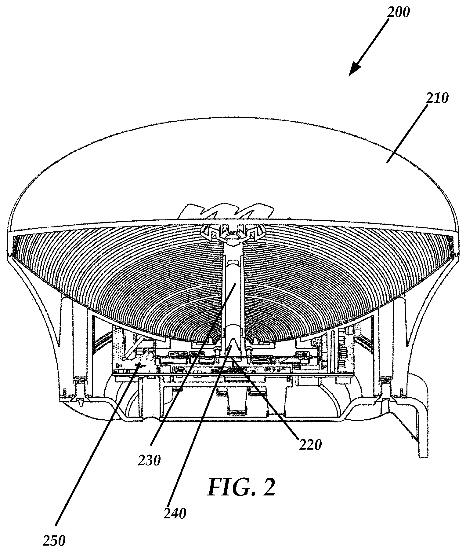
FIG. 2 is a cross sectional view of an example device constructed in accordance with the present disclosure. The example device comprises a waveguide of transitional cross section along its length, and having both a polygonal cross sectional area and a cylindrical cross sectional area. This waveguide is incorporated into a reflector antenna.
FIG. 3 is a top down view of an example device constructed in accordance with the present disclosure.
FIG. 4 is a cross sectional assembly view of an example device constructed in accordance with the present disclosure.
FIG. 5 is a perspective view of an example device constructed in accordance with the present disclosure.
FIG. 6 is a top down view of an example device constructed in accordance with the present disclosure.
DESCRIPTION OF EXEMPLARY EMBODIMENTS
Generally, the present disclosure provides higher polarization isolation solutions for waveguides that are mounted directly to a printed circuit board (PCB) or otherwise coupled to the PCB. Specifically, in some embodiments, the present disclosure utilizes one or more cross sections of a given waveguide to ease signal transition. Waveguides can have any variety of geometrical shapes and cross sections. The shape and/or cross section of a waveguide can be continuous along its length or can vary according to various design requirements. For instance, cross sections can be polygonal, conical, cylindrical, rectangular, elliptical square or circular, just to name a few.
The current practice is to excite a waveguide with a probe or monopole antenna. The probe can be a wire attached to a coaxial transmission or a feature embedded in a PCB. Typically, a PCB can be created with probes on the circuit board. A waveguide is then mounted directly to the PCB at approximately 90 degrees.
When probes are used to excite a waveguide, it is often convenient to place them on the same plane. In a circular waveguide, this results in limited isolation between orthogonal polarizations. A typical isolation is -20 dB using this type of configuration. One issue that arises with this practice is that electric fields inside a circular waveguide are not constrained to a particular direction as they are in a polygonal (square) waveguide. Small deviations inside the circular waveguide easily disturb the electrical field direction and thus degrade the isolation between orthogonal signals. Probes that are inserted into a circular waveguide are not symmetric and thus they disturb the otherwise orthogonal fundamental fields.
In contrast to the current practice, in some embodiments, the present disclosure provides a polygonal (square) waveguide as a transition region before the circular waveguide to improve isolation compared to what is practical with co-planar probes in a circular waveguide. Specifically, fields in a square waveguide are constrained to remain perpendicular to the waveguide walls and thus are not as free to change orientation as if they would be in a circular waveguide. The introduction of a square waveguide cross sectional area as a transition greatly improves the signal isolation that can be realized. As mentioned before, coplanar probes in a circular waveguide typically achieve -20 dB of isolation. With a square waveguide cross sectional area, signal isolation can increased to -40 dB and the signals can be much more clearly separated. In other words, 100 times improvement is achieved utilizing a square waveguide cross sectional area. The square waveguide cross sectional area resists the tendency for non-symmetric probes to cause polarization rotation which in turn increases polarization isolation. When the probes are coplanar in a circular cross sectional area there is an opportunity for the electric fields to rotate reducing cross polarization isolation. In a square waveguide the boundary condition for fields termination on the wall are held in a single plane and cannot rotate as a circular of curved wall allows.
The present disclosure provides three noteworthy features. First, the methods and systems described herein provide improved higher polarization isolation, which allows for better separation of two signals as they are transmitted in space. In other words, the two signals will interact with each other less. As mentioned earlier, higher isolation of approximately -40 dB is achieved using the embodiments of this present disclosure, which is a 100 times improvement from the current practice of -20 dB. Further details regarding this improvement will be discussed later herein.
In a second aspect, the present disclosure provides an improved matching with the addition of dialectic material (such as in a dielectric block) around the PCB launch. That is, the process works better than conventional processes because there is a gentler transition of sending signals out of the PCB launched in the waveguide and reinjecting them. To be sure, the dielectric block can be a matching component of the waveguide where it is used at the circular cross sectional area and the square cross sectional area of the waveguide. The dielectric block can be a matching component of the waveguide to match the PCB and the waveguide interface.
As a third feature of the present disclosure, various probes could be used, either in 3D or as shapes printed on a PCB. As will be explained further in this paper, in some embodiments, the dielectric filling does not need to be present. In other cases, dielectric filling can be used to support 3D probes. In further cases, the dielectric block is more convenient when it comes to precisely positioning probes inside the waveguide, which is occasionally used as a technique to supply and launch signals into the waveguide.
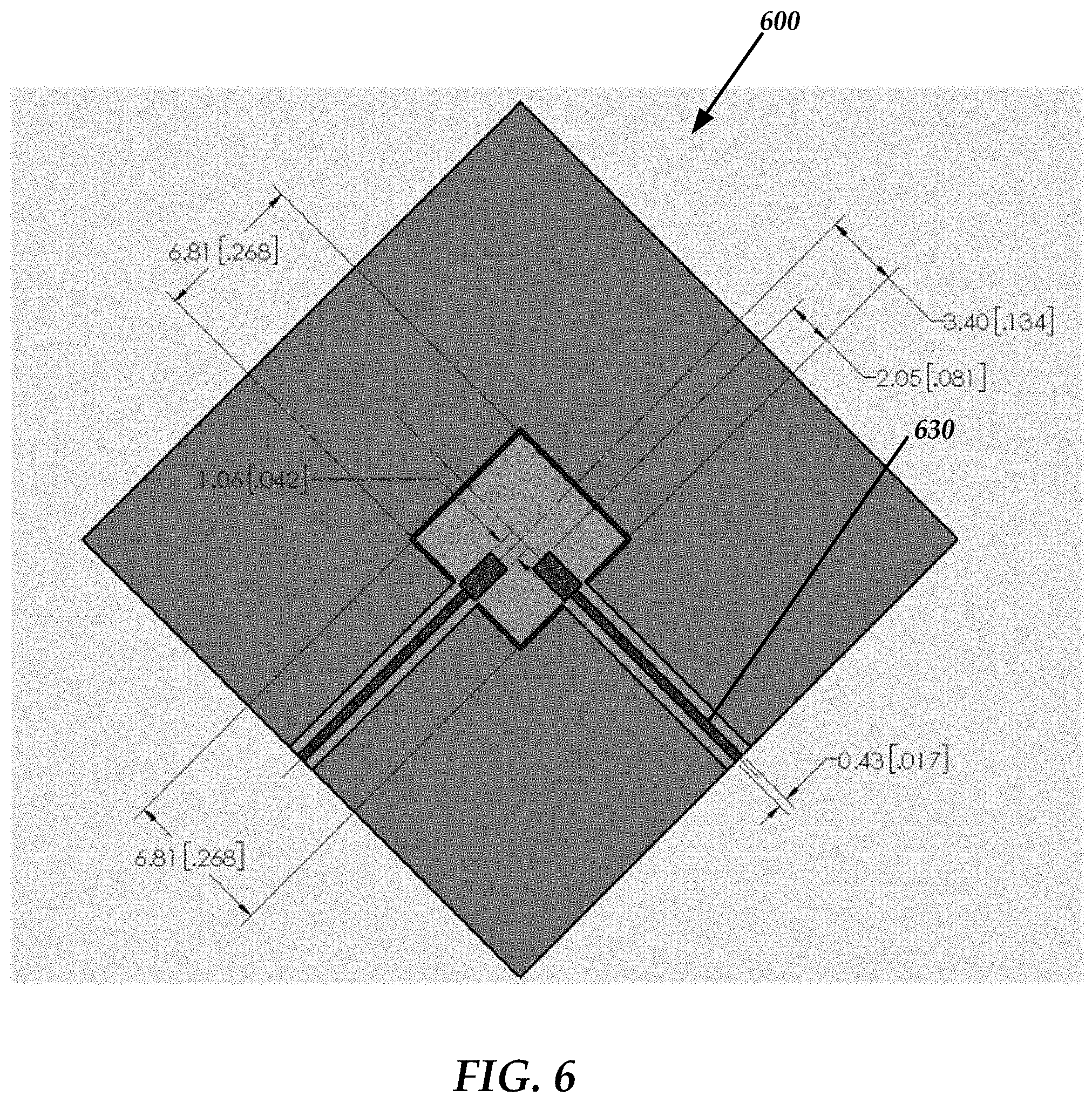
In some embodiments, the probes are made of wire which are soldered directly onto the circuit board and pressed in with the dielectric block. The probes could have a flatten replica right on the PCB itself. Instead of a rod shaped probe, it may be a flat piece of conductor built on the PCB. The probe can be included on the PCB on a two dimensional sheet rather than a three dimensional rod. An example of this can be viewed in FIG. 6, discussed below.
It should be noted that the present disclosure contemplates embodiments where a waveguide has a first cross sectional area and a second cross sectional area. The first cross sectional area and the second cross sectional area differ from each other. These cross sections may have different shapes, forms, types, or configurations. By having the signals pass through two separate waveguide cross sectional areas that differ from one another, the signal transition may be easier and less abrupt. These and other advantages of the present disclosure are described in greater detail infra. Further discussion regarding different types of waveguides can be found in U.S. Nonprovisional patent application Ser. No. 15/403,085, filed on Jan. 10, 2017, which is hereby incorporated by reference herein including all references cited therein.
Turning now to the figures, FIGS. 1A and 1B depict an example device 100 that is constructed in accordance with the present disclosure. Specifically, these figures depict the transition where the signals are led either on or off of the PCB into the structure for the antenna (not shown). The device 100 comprises a waveguide having a circular (cylindrical) waveguide cross sectional area 110 and a square transition waveguide cross sectional area 120. The square transition waveguide cross-sectional area 120 may also include one or more connectors. The device 100 can include additional or fewer components than those illustrated.
The coaxial connectors can launch signals into the PCB (not shown in FIGS. 1A and 1B). The PCB is preferably sandwiched between the circular waveguide cross sectional area 110 and the square transition waveguide cross sectional 120. A more detailed view of this can be found in the assembly view provided in FIG. 4, which shows a PCB 420 is sandwiched in between the circular waveguide cross sectional area 110 and the square transition waveguide cross sectional 120. Further details regarding FIG. 4 and the particular components of the device are provided later herein.
Referring still to FIGS. 1A and 1B, inside the circular waveguide is a square aperture which can mate with a waveguide that has a circular aperture which has a sharp edge. A conical shaped piece 124 of dielectric in that area is used to smooth the transition.
As described earlier, the present disclosure is directed to a device that transitions signals using a waveguide including a first cross sectional area and a second cross sectional area, the first and second cross sectional areas differing from either other. In some embodiments, the first cross sectional areas has a circular or cylindrical configuration and the second waveguide has a polygonal or square configuration. In some embodiments, the waveguide can comprise two sections of different size and/or cross section from one another.
FIG. 2 provides a cross sectional view of an example device 200 constructed in accordance with the present disclosure. The device 200 comprises an integrated antenna, radio, and transceiver both for transmitting and receiving data signals. In some embodiments, the device 200 can be a 24 GHz back-haul radio. The device 200 can communicate with a similar device located miles away. In some embodiments, the antenna is approximately 255 mm in diameter and is coupled with two printed circuit transmission lines (i.e. feed strips). In various embodiments, the use of two feed lines (or feed lines and coaxial cables) allows for dual linear (or dual circular) polarization. Additional feeds could be used to excite multiple, higher order modes in a particular waveguide. Indeed, feed lines/strips as well as coaxial cables as described herein can be generally referred to as an electrical feed.
The waveguide contains radiation produced by the antenna and directs the radiation along a path that is coaxial with a centerline X of the waveguide, in some embodiments.
In some embodiments, the antenna is coupled with a coaxial cable to a signal source such as a radio. In other embodiments, the antenna is coupled to a radio with a PCB based transmission line or feed strip. In some embodiments, the coaxial cable is used in place of the feed strip. In some embodiments, the coaxial cable is used in combination with one or more feed strips. The feed strip can comprise a printed circuit transmission line, in some embodiments.
Advantageously, the device 200 provides high levels of signal isolation between adjacent feeds, in various embodiments. The device 200 can also allow for linear or circular waves to be easily directed as desired. A narrow or wide bandwidth transition can be utilized, in some embodiments.
The waveguide of the device 200 can direct energy out onto the curved surface that is a parabolic reflector 210. The dielectric substrate can comprise any suitable PCB (printed circuit board) substrate material constructed from, for example, one or more dielectric materials. The antenna is mounted onto the dielectric substrate. In one embodiment the antenna is a patch antenna. In another embodiment, the antenna is a multi-stack set of antennas. In some embodiments, the antenna is electrically coupled with one or more printed circuit transmission lines.
The example device 200 comprises a waveguide of transitional cross section along its length. The waveguide depicted has both a polygonal cross sectional 220 area and a cylindrical cross sectional area 230. In other words, the waveguide of FIG. 2 has a first section that has a polygonal cross section and a second section that has a cylindrical cross section. A transition section 240 couples the first section and the second section of the waveguide. The transition section 240 allows the shape of the signal radiation that is emitted to be changed. For example, the transition section 240 can be in the form of a square 220 with a conical shape mounted on it or otherwise coupled to it, while the waveguide includes a circular cross sectional area 230, such as illustrated in FIG. 2. Thus, in this embodiment, the square 220 is tapered into a conical shape, and allowed to gradually decrease until it disappears. This is the area where there is a transition between the propagation the polygonal cross sectional 220 area in relation to the cylindrical cross sectional area 230.
Referring still to FIG. 2, the square 220 can be a dialectic block to ease the transition from the PCB into the waveguide, and also further down, the dielectric block can be used to ease the transition between the square waveguide cross sectional area 220 and the circular waveguide cross sectional area 230. This allows for optimum radiation reflection and symmetry near the antenna, while providing a desired emitted signal shape through the transition section 240.
The waveguide contains radiation produced by the antenna and directs the radiation along a path that is coaxial with a centerline X of the waveguide, in some embodiments.
While the waveguide is generally elongated, the waveguide can comprise a truncated or short embodiment of a waveguide.
For context, without the waveguide, the antenna emits signal radiation in a plurality of directions, causing loss of signal strength, reduced signal directionality, as well as cross-port interference (e.g., where an adjacent antenna is affected by the antenna).
In various embodiments, the waveguide of the device 200 is mounted directly to the dielectric substrate 250, around a periphery of the antenna. The spacing between the waveguide and the antenna can be varied according to design parameters.
In one embodiment the waveguide encloses the antenna and captures the radiation of the antenna, directing it along and out of the waveguide. The waveguide is constructed from any suitable conductive material. The use of the waveguide allows one to transfer signals from one location to another location with minimal loss or disturbance of the signal.
In various embodiments, the length of the waveguide is selected according to design requirements, such as required signal symmetry. The waveguide can have any desired shape and/or size and length. The illustrated waveguide is circular in shape, but any polygonal, cylindrical, or irregular shape can be implemented as desired.
In various embodiments, the selection of dielectric materials for the waveguide can be used to effectively adjust a physical size of components of the device 200 while keeping the electrical characteristics compatible. Notably, a wavelength in dielectric makes objects smaller than they would be in a vacuum so the components or parts of the device 100 may shrink in size. Typically there is a sharp transition between the PCB material and the air vacuum that causes reflections instead of radiation. By placing a dielectric block on either side of the PCB, the transition is eased to ensure a gentler, less abrupt transition. In other words, this results in a less abrupt change in the propagation characteristics resulting in fewer reflections and less interference as they move throughout the device.
The present disclosure also includes embodiments where the device includes multiple dielectric pieces in different cross sections of a waveguide, in order to ease signal transition. If the signal hits the transition the amount of energy reflected in that transition corresponds to how much the dielectric constant changes on one side of the transition in comparison to the other side. Thus, the reflections are much reduced if signals experience propagation changes through are a plurality of smaller steps instead of one big step.
It also should be noted that with the appropriate thicknesses, the reflections of one transition can be arranged to cancel the reflections from a subsequent reflection. Thus, for instance, the conical shape mounted onto the square transition cross section area could vary in length, be it longer or shorter. The conical shape has a flat end with which one could control the magnitude and direction of a reflection in such a way that it cancels all the other reflections. In other words, the conical shape can be used as a tuning tool to cancel other reflections, which is an improvement above the current practice.
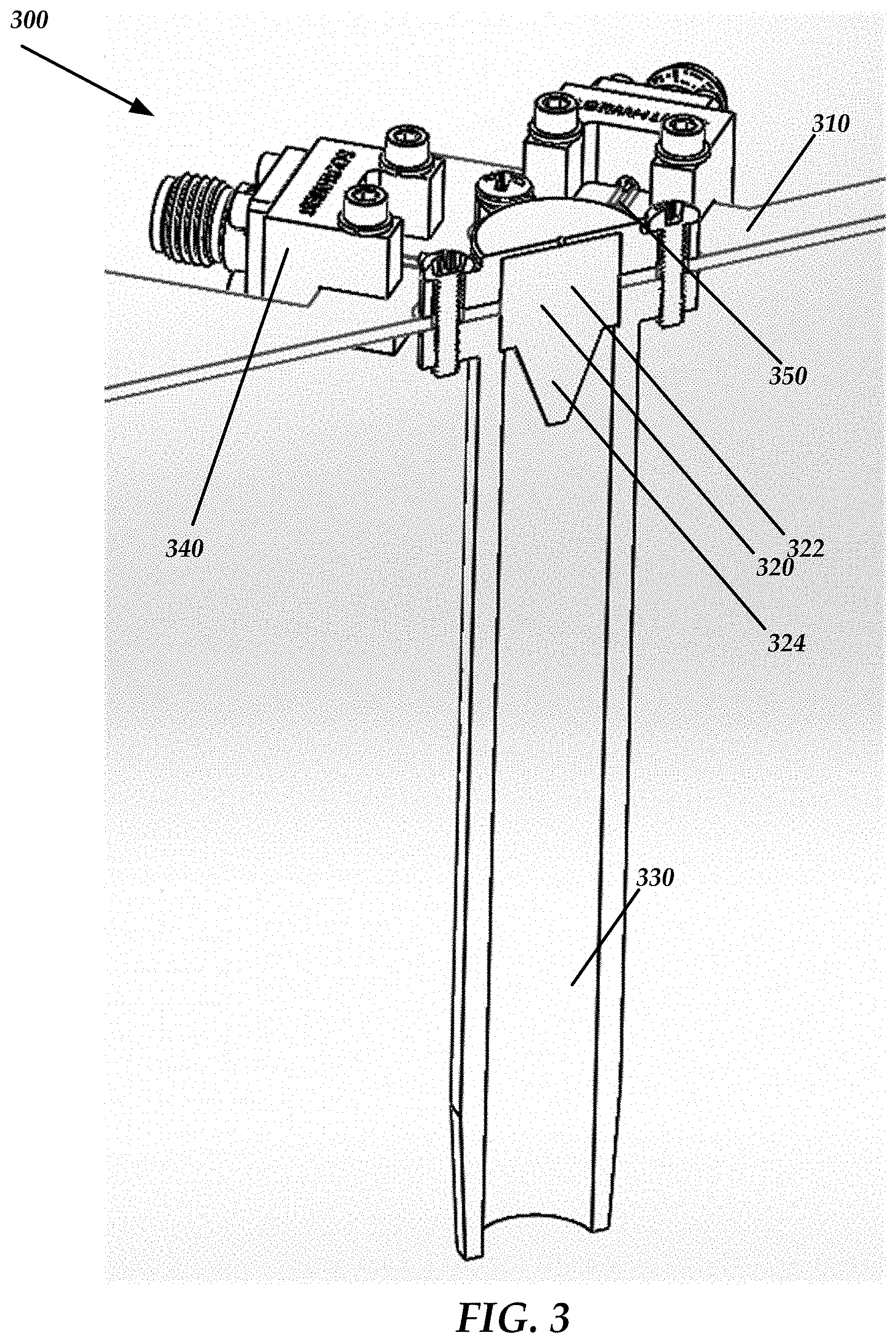
Turning now to FIG. 3, FIG. 3 is exemplary view of the device 300 which provides an enlarged, more detailed perspective view of a portion of FIG. 2. Specifically, FIG. 3 depicts a waveguide having a circular waveguide cross sectional area 330 and a square transition waveguide cross sectional area 320 comprising a dielectric block 322. As described previously, the square transition waveguide cross sectional area 320 may include a conical shape with a tapered end 324, which allows for the gentler transition of signals as they pass through the waveguide cross sectional areas which differ from each other. The gentler transition of signals in turn provides higher isolation. The device 300 also includes two coaxial connectors 340 to the PCB. The device 300 is not limited to the number of components as depicted in FIG. 3.
FIG. 4 is a cross sectional assembly view of a device 400. As mentioned earlier, FIG. 4 shows a printed circuit board (PCB) 420 that is sandwiched in between the circular waveguide cross sectional area 110 and the square transition waveguide cross sectional area 120. When constructed, the circular waveguide cross sectional area 110 and the square transition waveguide cross sectional area 120 can provide a smooth, easier transition as described above. The device 400 also comprises a top layer 410 and a bottom layer 430 which hold the assembly of the PCB and the components of the device 400 together.
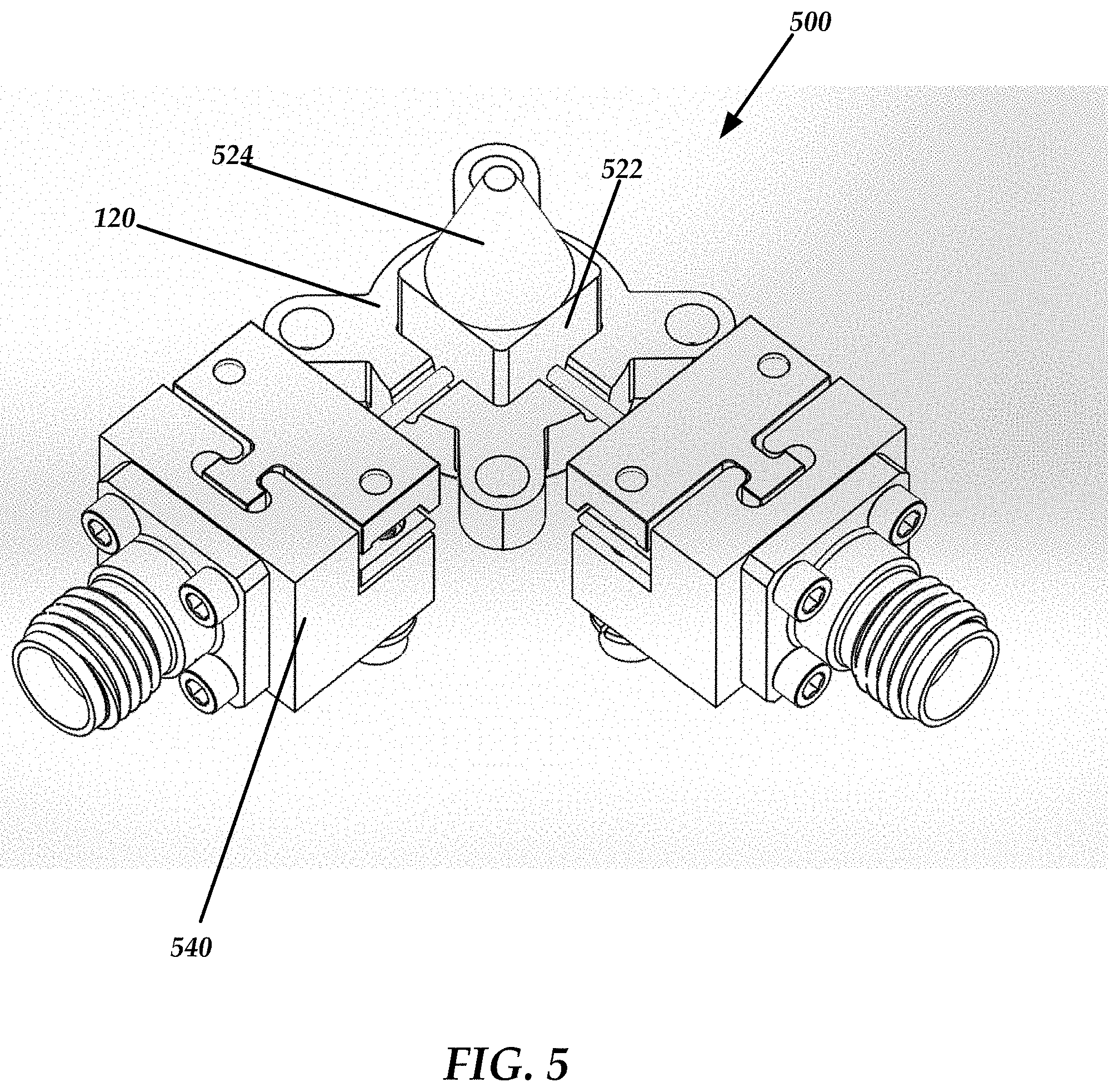
FIG. 5 is a perspective view of an example device 500 in accordance with some embodiments of the present disclosure. Referring to FIGS. 1A, 1B and 5, the device 500 comprises a waveguide having a circular (cylindrical) waveguide cross sectional area 110 and a square transition waveguide cross sectional area 120. The square transition section 120 may include a square waveguide cross sectional area 522 with a conical shape waveguide cross section 524 mounted on it or otherwise coupled to it. The square transition waveguide cross-sectional area 120 may also include one or more connectors 540. The device 500 can include additional or fewer components than those illustrated.
The coaxial connectors 540 are connectors to the PCB, and they can launch signals into the PCB (not shown in FIGS. 1A and 1B). The PCB is preferably sandwiched between the circular waveguide cross sectional area 110 and the square transition waveguide cross sectional area 120.
FIG. 6 is a top down view of a dielectric substrate 600 in accordance with some embodiments of the present disclosure. As discussed briefly above, probes can be printed on a printed circuit board as depicted in FIG. 6. It should be noted that for purposes of the present disclosure, wider probes having a triangular shape or a squatty appearance can have much more bandwidth than a skinny probe at the same overall length.
In an alternative embodiment, the addition of dielectric material could be applied to a coaxial feed transmission, thereby eliminating the need for a PCB altogether. In other words, instead of having coaxial transmissions that interface and transition signals into a PCB, one could bring a coaxial cable up through the wall of the waveguide, put it with a different connector for the dielectric substrate, strip out the PCB and show the connector.
While this technology is susceptible of embodiment in many different forms, there is shown in the drawings and will herein be described in detail several specific embodiments with the understanding that the present disclosure is to be considered as an exemplification of the principles of the technology and is not intended to limit the technology to the embodiments illustrated.
The terminology used herein is for the purpose of describing particular embodiments only and is not intended to be limiting of the technology. As used herein, the singular forms "a", "an" and "the" are intended to include the plural forms as well, unless the context clearly indicates otherwise. It will be further understood that the terms "comprises" and/or "comprising," when used in this spe
References
D00000
D00001
D00002
D00003
D00004
D00005
D00006
XML
uspto.report is an independent third-party trademark research tool that is not affiliated, endorsed, or sponsored by the United States Patent and Trademark Office (USPTO) or any other governmental organization. The information provided by uspto.report is based on publicly available data at the time of writing and is intended for informational purposes only.
While we strive to provide accurate and up-to-date information, we do not guarantee the accuracy, completeness, reliability, or suitability of the information displayed on this site. The use of this site is at your own risk. Any reliance you place on such information is therefore strictly at your own risk.
All official trademark data, including owner information, should be verified by visiting the official USPTO website at www.uspto.gov. This site is not intended to replace professional legal advice and should not be used as a substitute for consulting with a legal professional who is knowledgeable about trademark law.