Methods of forming interdigitated back contact layers
Nemeth , et al.
U.S. patent number 10,714,652 [Application Number 16/014,695] was granted by the patent office on 2020-07-14 for methods of forming interdigitated back contact layers. This patent grant is currently assigned to Alliance for Sustainable Energy, LLC. The grantee listed for this patent is Alliance for Sustainable Energy, LLC. Invention is credited to Vincenzo Anthony LaSalvia, William Michael Nemeth, Matthew Robert Page, Pauls Stradins, David Levi Young.


| United States Patent | 10,714,652 |
| Nemeth , et al. | July 14, 2020 |
Methods of forming interdigitated back contact layers
Abstract
Methods of forming interdigitated back contact (IBC) layers are provided. According to an aspect of the invention, a first layer having alternating regions of n-type amorphous hydrogenated silicon and p-type amorphous hydrogenated silicon is formed on a second layer of intrinsic amorphous hydrogenated silicon. The first layer and the second layer are then annealed, such that dopants from the first layer diffuse into the second layer, and the first layer and the second layer crystallize into polysilicon.
| Inventors: | Nemeth; William Michael (Wheat Ridge, CO), Stradins; Pauls (Golden, CO), LaSalvia; Vincenzo Anthony (Conifer, CO), Page; Matthew Robert (Littleton, CO), Young; David Levi (Golden, CO) | ||||||||||
|---|---|---|---|---|---|---|---|---|---|---|---|
| Applicant: |
|
||||||||||
| Assignee: | Alliance for Sustainable Energy,
LLC (Golden, CO) |
||||||||||
| Family ID: | 64693632 | ||||||||||
| Appl. No.: | 16/014,695 | ||||||||||
| Filed: | June 21, 2018 |
Prior Publication Data
| Document Identifier | Publication Date | |
|---|---|---|
| US 20180374984 A1 | Dec 27, 2018 | |
Related U.S. Patent Documents
| Application Number | Filing Date | Patent Number | Issue Date | ||
|---|---|---|---|---|---|
| 62522777 | Jun 21, 2017 | ||||
| Current U.S. Class: | 1/1 |
| Current CPC Class: | H01L 31/022458 (20130101); H01L 31/0745 (20130101); H01L 31/077 (20130101); H01L 31/1872 (20130101); H01L 31/182 (20130101); H01L 31/1804 (20130101); H01L 31/022441 (20130101); H01L 31/0682 (20130101); Y02E 10/546 (20130101); Y02E 10/547 (20130101); Y02P 70/50 (20151101) |
| Current International Class: | H01L 31/18 (20060101); H01L 31/077 (20120101); H01L 31/0224 (20060101); H01L 31/068 (20120101); H01L 31/0745 (20120101) |
References Cited [Referenced By]
U.S. Patent Documents
| 4897123 | January 1990 | Mitsui |
| 6166320 | December 2000 | Nagashima et al. |
| 6340788 | January 2002 | King et al. |
| 8242354 | August 2012 | Smith |
| 8614395 | December 2013 | Nielson et al. |
| 2010/0307591 | December 2010 | Bedell et al. |
| 2012/0107997 | May 2012 | Kim et al. |
| 2012/0305072 | December 2012 | Fujimori et al. |
| 2014/0209149 | July 2014 | Mascarenhas et al. |
| 2014/0295613 | October 2014 | O'Sullivan |
| 2015/0162478 | June 2015 | Fafard et al. |
| 2015/0162483 | June 2015 | Weidman |
| 2016/0020342 | January 2016 | Heng |
| 2018/0374977 | December 2018 | Geerligs et al. |
Other References
|
Almansouri, I. et al., "Supercharging Silicon Solar Cell Performance by Means of Multijunction Concept," IEEE Journal of Photovoltaics, vol. 5, No. 3, May 2015, pp. 968-976. cited by applicant . Bush, K. et al., "23.6%-efficient monolithic perovskite/silicon tandem solar cells with improved stability," Nature Energy, vol. 2, 2017, pp. 1-7. cited by applicant . Cariou, R. et al., "Monolithic Two-Terminal III-V//Si Triple-Junction Solar Cells With 30.2% Efficiency Under 1-Sun AM 1.5g," IEEE Journal of Photovoltaics, vol. 7, No. 1, Jan. 2016, pp. 367-373. cited by applicant . Deppe, D.G., "Thermodynamic explanation to the enhanced diffusion of base dopant in AlGaAs--GaAs npn bipolar transistors," American Institute of Physics, vol. 56, No. 370, 1990, 3 pages. cited by applicant . Das, U. et al., "The role of back contact patterning on stability and performance of Si IBC heterojunction solar cells," IEEE, 2014, pp. 0590-0593. cited by applicant . Duong, T., "Rubidium Multication Perovskite with Optimized Bandgap for Perovskite-Silicon Tandem with over 26% Efficiency," Advanced Energy Materials, vol. 7, 2017, 11 pages. cited by applicant . Essig, S. et al., "Progress towards a 30% efficient GaInP/Si tandem solar cell," Energy Procedia, vol. 77, 2015, pp. 464-469. cited by applicant . Essig, S. et al., "Realization of GaInP/Si Dual-Junction Solar Cells With 29.8% 1-Sun Efficiency," IEEE Journal of Photovoltaics, vol. 6, No. 4, Jul. 2016, pp. 1012-1019. cited by applicant . Essig, S. et al., "Boosting the efficiency of III-V/Si tandem solar cells," 43rd IEEE Photovoltaic Specialists Conference, Jun. 2016, pp. 2040-2042. cited by applicant . Essig, S. et al., "Mechanically stacked 4-terminal III-V/Si tandem solar cells," 44th IEEE Photovoltaics Conference, 2017, 2 pages. cited by applicant . Gee, J. et al., "A 31%-Efficient GaAs/Silicon Mechanically Stacked, Multijunction Concentrator Solar Cell," IEEE Electron Device Letters, 1988, pp. 754-758. cited by applicant . Geisz, J. et al., "Enhanced external radiative efficiency for 20.8% efficient single-junction GaInP solar cells," Applied Physics Letters, vol. 3, 2013, pp. 041118-1 through 041118-5. cited by applicant . Green, M. et al., "Solar cell efficiency tables (version 49), Progress in Photovoltaics: Research and Applications," vol. 25, 2017, pp. 3-13. cited by applicant . Haase, F. et al., "Interdigitated back contact solar cells with polycrystalline silicon on oxide passivating contacts for both polarities," Japanese Journal of Applied Physics, vol. 56, 2017, 5 pages. cited by applicant . Hamon, G. et al., "Direct Growth of Crystalline Silicon on GaAs by Low Temperature PECVD: Towards Hybrid Tunnel Junctions for III-V/Si Tandem Cells," 43rd IEEE Photovoltaics Specialists Conference, Jun. 2016, pp. 1895-1897. cited by applicant . Herasimenka, S. et al., "A Simplified Process Flow for Silicon Heterojunction Interdigitated Back Contact Solar Cells: Using Shadow Masks and Tunnel Junctions," IEEE, 2014, pp. 2486-2490. cited by applicant . Hong, C.Y. et al., "Back-Contacted Thin-Film GaAs Solar Cells," IEEE PVSC Conference, Jun. 5-10, 2016, Portland, Oregon, pp. 3629-3631. cited by applicant . Jain, N. et al., "Development of Lattice-Matched 1.7 eV GaInAsP Solar Cells grown on GaAs by MOVPE," IEEE 43rd Photovoltaic Specialists Conference, 2016, pp. 0046-0051. cited by applicant . Jimeno, J. et al., "Upgrading the Silicon IBC to the 40% efficiency," 2016 IEEE PVSC Conference, 6 pages. cited by applicant . Kanechida, M. et al., "A Vertical Insulated Gate A1GaN/GaN Heterojunction Field-Effect Transistor," The Japan Society of Applied Physics, 2007, 3 pages. cited by applicant . Klein, T. et al., "Transparent Conductive Adhesives for Tandem Solar Cells," 44th IEEE Photovoltaics Conference, 2017, 6 pages. cited by applicant . Liu, H. et al., "The realistic energy yield potential of GaAs-on-Si tandem solar cells: a theoretical case study," Optics Express, vol. 23, No. 7, Apr. 6, 2015, p. A382. cited by applicant . NREL Best Research-Cell Efficiencies Chart, accessed Aug. 23, 2018, https://www.nrel.gpv/pv/assets/images/efficiency-chart.png, 1 page. cited by applicant . Nagashima, T. et al., "Three-Terminal Tandem Solar Cells With a Back-Contact Type Bottom Cell," 28th IEEE Photovoltaic Specialists Conference, 2000, pp. 1193-1196. cited by applicant . Nagashima, T. et al., "Surface Passivation for Germanium and Silicon Back Contact Type Photovoltaic Cells," IEEE 4th World Conference on Photovoltaic Energy, May 2006, pp. 655-658. cited by applicant . Onno, A. et al., "Simulation study of GaAsP/Si tandem solar cells," Solar Energy Materials & Solar Cells, vol. 145, 2016, pp. 206-216. cited by applicant . Richter, A. et al., "Reassessment of the Limiting Efficiency for Crystalline Silicon Solar Cells," IEEE Journal of Photovoltaics, vol. 3, No. 4, Oct. 2013, 8 pages. cited by applicant . Rienacker, M. et al., "Junction Resistivity of Carrier-Selective Polysilicon on Oxide Junctions and Its Impact on Solar Cell Performance," IEEE Journal of Photovoltaics, vol. 7, No. 1, Jan. 2017, pp. 11-14. cited by applicant . Scherff, M., Novel Methode for Preparation of Interdigitated Back Contacted a-Si:H/c-Si Heterojunction Solar Cells, preprint to be published in the proceedings of the 26th European Photovoltaic Solar Energy Conference, Sep. 5-9, 2011, Hamburg, Germany, 5 pages. cited by applicant . Schnabel, M. et al., "III-V/Si Tandem Cells Utilizing Interdigitated Back Contact Si Cells and Varying Terminal Configurations," IEEE 44th Photovoltaic Specialists Conference, 2017, 7 pages. cited by applicant . Takamoto, T. et al., "Mechanism of Zn and Si diffusion from a highly doped tunnel junction for InGaP/GaAs tandem solar cells," Journal of Applied Physics, vol. 85, No. 3, Feb. 1, 1999, 6 pages. cited by applicant . Tomasi, A. et al., "Photolithography-free Interdigitated Back-Contacted Silicon Heterojunction Solar Cells with Efficiency >21%," IEEE, 2014, pp. 3644-3648. cited by applicant . Warren, E. et al., "Modeling three-terminal III-V/Si tandem solar cells," submitted to 44th IEEE Photovoltaics Conference, 2017, 4 pages. cited by applicant . Yang, G. et al., "IBC c-Si solar cells based on ion-implanted poly-silicon passivating contacts," Solar Energy Materials & Solar Cells, vol. 158, 2016, pp. 84-90. cited by applicant . Yoshikawa, K. et al., "6 inch High Efficiency Back Contact Crystalline Si Solar Cell Applying Heterojunction and Thinfilm Technology," 43rd Photovoltaic Specialists Conference, Jun. 2016, pp. 3366-3369. cited by applicant. |
Primary Examiner: Landau; Matthew C
Assistant Examiner: Yemelyanov; Dmitriy
Attorney, Agent or Firm: Barkley; Sam J.
Government Interests
CONTRACTUAL ORIGIN
The United States Government has rights in this invention under Contract No. DE-AC36-08GO28308 between the United States Department of Energy and Alliance for Sustainable Energy, LLC, the Manager and Operator of the National Renewable Energy Laboratory.
Parent Case Text
CROSS-REFERENCE TO RELATED APPLICATION
This application claims priority under 35 U.S.C. .sctn. 119 to U.S. Provisional Patent Application No. 62/522,777 filed on Jun. 21, 2017, the contents of which are hereby incorporated by reference in their entirety.
Claims
What is claimed is:
1. A method comprising: forming a first layer comprising alternating regions of n-type amorphous hydrogenated silicon and p-type amorphous hydrogenated silicon on a second layer comprising intrinsic amorphous hydrogenated silicon; and diffusing such that dopants from the first layer diffuse into the second layer; and crystallizing the first layer and the second layer into polysilicon by annealing the first layer and the second layer at a temperature between 650.degree. C. and 850.degree. C.; and wherein before the forming of the first layer, depositing the second layer on a third layer comprising silicon oxide; and wherein before the annealing, the first layer further comprises gaps between adjacent regions of the n-type amorphous hydrogenated silicon and the p-type amorphous hydrogenated silicon: and wherein, after the annealing, the second layer comprises alternating regions of n-type polycrystalline silicon, intrinsic polycrystalline silicon, and p-type polycrystalline silicon; and wherein the first layer is formed by plasma-assisted chemical vapor deposition (PECVD).
2. The method according to claim 1, wherein the first layer is formed by: using a first shadow mask to deposit the regions of the n-type amorphous hydrogenated silicon; and depositing the regions of the p-type amorphous hydrogenated silicon using a second shadow mask.
3. A method for using a shadow mask to form a layer of polycrystalline silicon with alternating doping types in a photovoltaic device comprising interdigitated back contact layers of a first layer comprising alternating regions of n-type amorphous hydrogenated silicon and p-type amorphous hydrogenated silicon and further comprising a second layer comprising intrinsic amorphous hydrogenated silicon; and wherein the method comprises crystallizing and diffusing a dopant by annealing the first layer and the second layer at a temperature between 650.degree. C. and 850.degree. C.; and wherein the method further comprises depositing a second layer comprising intrinsic amorphous hydrogenated silicon; patterning a first layer comprising alternating regions of n-type amorphous hydrogenated silicon and p-type amorphous hydrogenated silicon; and wherein, before the forming of the first layer, depositing the second layer on a third layer comprising silicon oxide; and wherein the first layer is formed by depositing the regions of the n-type amorphous hydrogenated silicon by using a first shadow mask; and depositing the regions of the p-type amorphous hydrogenated silicon by using a second shadow mask; and wherein, before the annealing, the first layer further comprises gaps between adjacent regions of the n-type amorphous hydrogenated silicon and the p-type amorphous hydrogenated silicon.
Description
BACKGROUND
The present invention relates to methods of forming interdigitated back contact (IBC) layers that may be used in photovoltaic (PV) devices. IBC solar cells are the most efficient Si solar cells today. In IBC solar cells, both junctions that collect positive and negative photocarriers are on the back of the cell, while the front has no grid and thus no shading losses. However, the dopant patterning required for these back junctions is challenging. Heavily doped p-type and heavily doped n-type regions should be separated by a highly resistive gap that may be made of intrinsic polysilicon or another dielectric material, otherwise the cell may be shunted. Further, the doped regions should be several hundred microns wide with well-defined edges, in order not to shunt across the undoped gap. Thus, reliable, precise, and inexpensive dopant patterning is needed for IBC solar cells.
Related art dopant patterning techniques include ion implantation through a mask, plasma immersion ion implantation (PIII) through a mask, and printed spin-on doping. However, these techniques can be costly, and may not be clean enough to enable high-efficiency IBC solar cells. Therefore, it would be advantageous to provide a simple, inexpensive, and precise dopant pattering technique that is compatible with solar cell processing.
SUMMARY
Exemplary embodiments of the invention provide methods of forming IBC layers. According to an aspect of the invention, a method includes forming a first layer having alternating regions of n-type amorphous hydrogenated silicon and p-type amorphous hydrogenated silicon on a second layer including intrinsic amorphous hydrogenated silicon. The method also includes annealing the first layer and the second layer such that dopants from the first layer diffuse into the second layer, and the first layer and the second layer crystallize into polysilicon. The annealing may be performed at a temperature greater than 650.degree. C.
Before the forming of the first layer, the second layer may be deposited on a third layer comprising silicon oxide. The first layer may be formed by using a first shadow mask to deposit the regions of the n-type amorphous hydrogenated silicon, and using a second shadow mask to deposit the regions of the p-type amorphous hydrogenated silicon.
Before the annealing, the first layer may include gaps between adjacent regions of the n-type amorphous hydrogenated silicon and the p-type amorphous hydrogenated silicon. After the annealing, the second layer may include alternating regions of n-type polycrystalline silicon, intrinsic polycrystalline silicon, and p-type polycrystalline silicon. The first layer may be formed by plasma-assisted chemical vapor deposition (PECVD).
In an aspect, disclosed is a method for using a deposited mask to form a layer of polycrystalline silicon with alternating doping types in a photovoltaic device having interdigitated back contact layers, the method includes blanketing with i/a-Si:H+SiNx; patterning and etching; removing photoresist; adding p/a-Si:H+SiNx; blanketing with n/a-Si:H+SiNx; precrystallizing; crystallizing a-Si:H into polySi; and diffusing a dopant. In an embodiment, the method also includes blanketing with i/a-Si:H+SiNx+i/aSi:H.
In another aspect, disclosed is a method for using a shadow mask to form a layer of polycrystalline silicon with alternating doping types in a photovoltaic device having interdigitated back contact layers, the method includes depositing i/a-Si:H; patterning a n/a-SiH deposition; patterning a p/a-Si:H deposition; crystallizing; and diffusing a dopant.
Other objects, advantages, and novel features of the present invention will become apparent from the following detailed description of the invention when considered in conjunction with the accompanying drawings.
BRIEF DESCRIPTION OF THE DRAWINGS
FIGS. 1A, 1B, 1C, 1D, 1E, 1F, 1G, 1H, 1I and 1J depict a method of using a deposited mask to form a layer of polycrystalline silicon with alternating doping types according to a first embodiment of the invention. FIG. 1A depicts a step of blanketing i/a-Si:H+SiNx. FIG. 1B depicts a step of patterning and etching. FIG. 1C depicts a step of removing photoresist (PR) and adding p/a-Si:H+SiNx. FIG. 1D depicts a step of patterning. FIG. 1E depicts a step of etching and liftoff. FIG. 1F depicts a step of blanketing with n/a-Si:H+SiNx. FIG. 1G depicts a step of patterning. FIG. 1H depicts a step of etching and liftoff. FIG. 1I depicts a step of precrystallizing. FIG. 1J depicts a step of crystallizing a-Si:H into polySi and dopant diffusion.
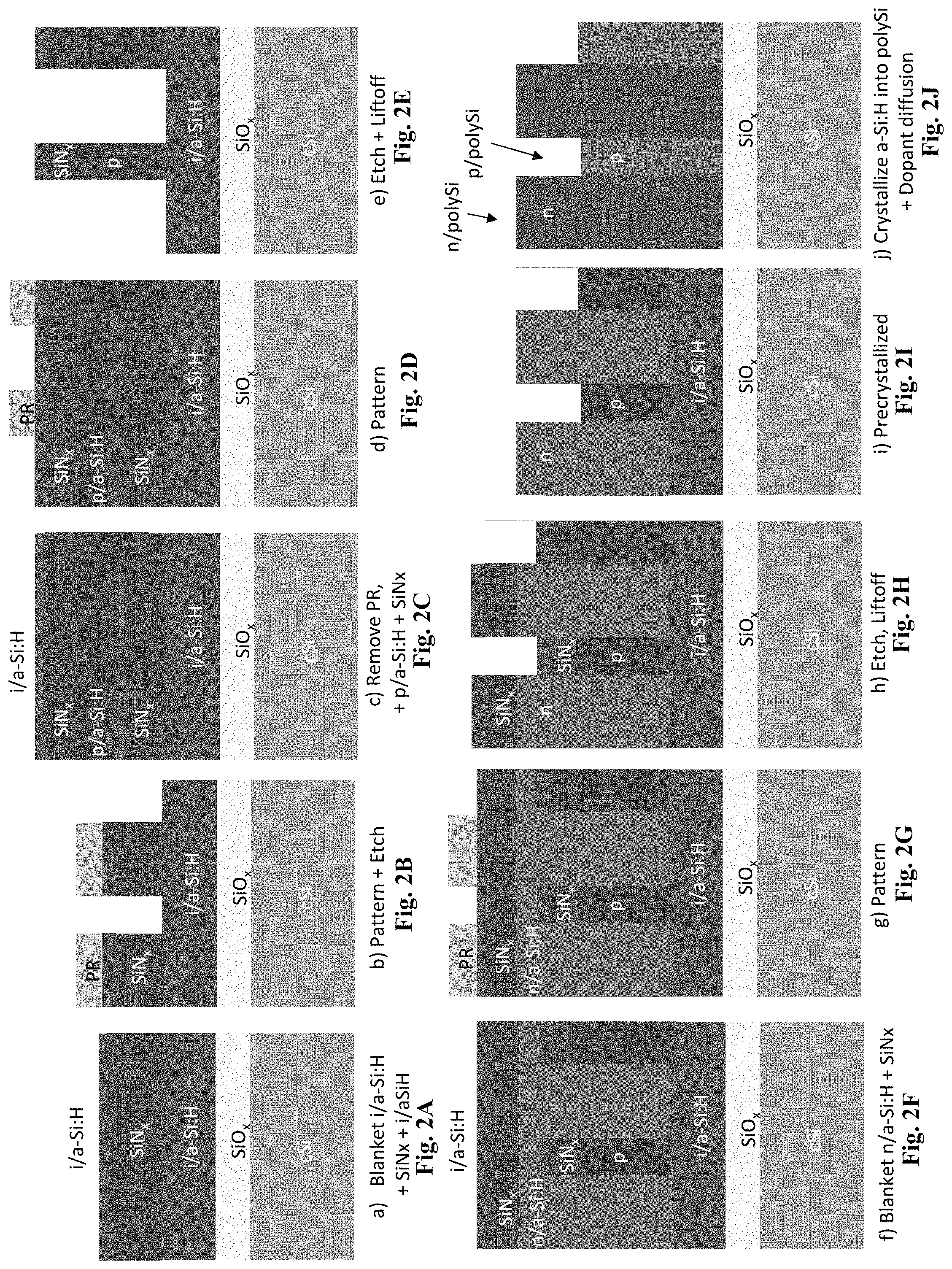
FIGS. 2A, 2B, 2C, 2D, 2E, 2F, 2G, 2H, 2I and 2J depict a method of using a deposited mask to form a layer of polycrystalline silicon with alternating doping types according to the first embodiment of the invention. FIG. 2A depicts a step of blanketing i/a-Si:H+SiNx+i/aSi:H. FIG. 2B depicts a step of patterning and etching. FIG. 2C depicts a step of removing PR and adding p/a-Si:H+SiNx. FIG. 2D depicts a step of patterning. FIG. 2E depicts a step of etching and liftoff. FIG. 2F depicts a step of blanketing with n/a-Si:H+SiNx. FIG. 2G depicts a step of patterning. FIG. 2H depicts a step of etching and liftoff. FIG. 2I depicts a step of precrystallizing. FIG. 2J depicts a step of crystallizing a-Si:H into polySi and dopant diffusion.
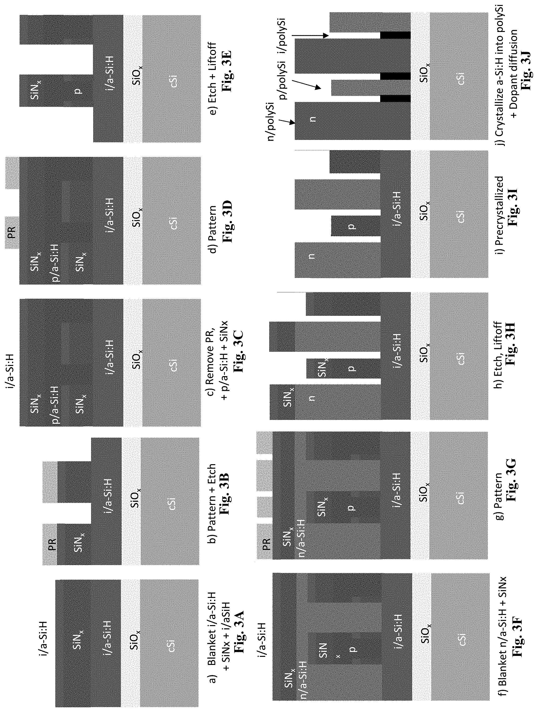
FIGS. 3A, 3B, 3C, 3D, 3E, 3F, 3G, and 3H, depict a method of using yet another method of using a deposited mask to form a layer of polycrystalline silicon with alternating doping types according to the first embodiment of the invention. FIG. 3A depicts a step of blanketing i/a-Si:H+SiNx+i/aSi:H. FIG. 3B depicts a step of patterning and etching. FIG. 3C depicts a step of removing PR and adding p/a-Si:H+SiNx. FIG. 3D depicts a step of patterning. FIG. 3E depicts a step of etching and liftoff. FIG. 3F depicts a step of blanketing with n/a-Si:H+SiNx. FIG. 3G depicts a step of patterning. FIG. 3H depicts a step of etching and liftoff. FIG. 3I depicts a step of precrystallizing. FIG. 3J depicts a step of crystallizing a-Si:H into polySi and dopant diffusion.
FIGS. 4A, 4B, 4C, and 4D depict a method of using a shadow mask to form a layer of polycrystalline silicon with alternating doping types according to a second embodiment of the invention. FIG. 4A depicts a step of i/a-Si:H deposition. FIG. 4B depicts a step of patterned n/a-SiH deposition. FIG. 4C depicts a step of patterned p/a-Si:H deposition. FIG. 4D depicts a step of crystallization and dopant diffusion.
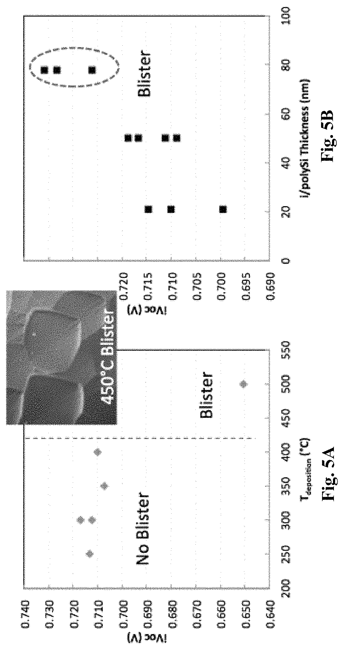
FIGS. 5A and 5B depict the passivation quality of intrinsic polycrystalline Si/SiO.sub.2 structures formed on n-Cz wafers according to exemplary embodiments of the invention. FIGS. 5A and 5B depict passivation quality of intrinsic poly-Si/SiO.sub.2 structures on KOH-planarized n-Cz wafers. FIG. 5A depicts intrinsic a-Si:H deposition temperature series. FIG. 5B depicts a-Si:H thickness series. The passivation is characterized by the iVoc after an 850.degree. C. crystallization anneal and H-passivation by Al.sub.2O.sub.3.
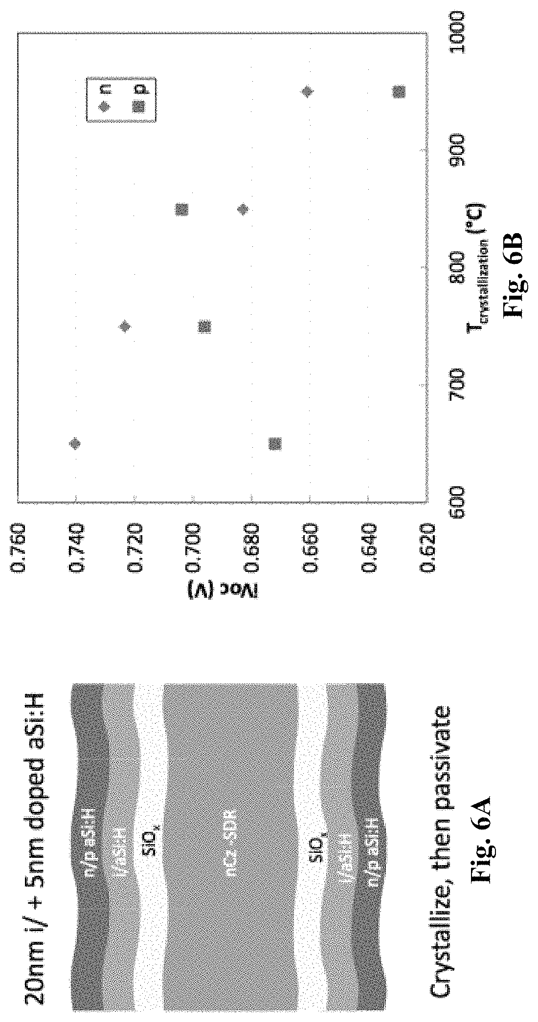
FIGS. 6A and 6B depict characteristics of high performance p-type and n-type passivated contacts that are produced according to exemplary embodiments of the invention. FIG. 6A depicts symmetric sandwich structures as precursors to passivated contacts. FIG. 6B depicts iV.sub.oc of these structures after crystallization/drive-in anneal at various temperatures, followed by passivation with Al.sub.2O.sub.3 as H-source layer.
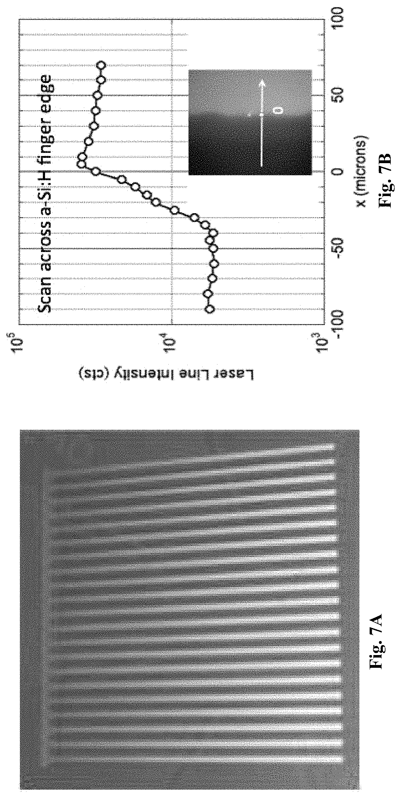
FIGS. 7A and 7B depict characteristics of an amorphous hydrogenated silicon film that was produced according to the second embodiment of the invention. FIG. 7A depicts a-Si:H film deposited on quartz through the BSF finger mask of the IBC cell. FIG. 7B depicts spatial edge fidelity of the BSF finger resolved by optical microreflectance scan.
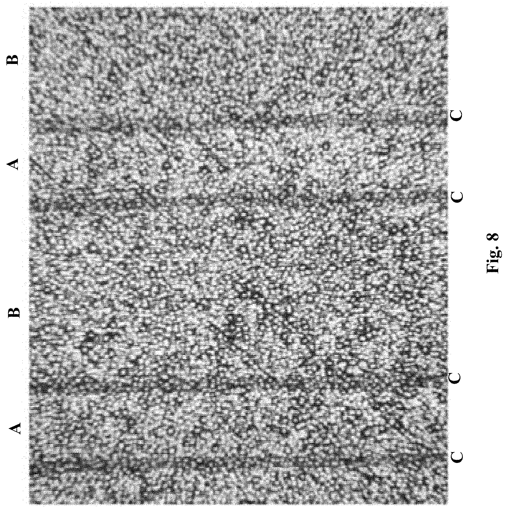
FIG. 8 depicts an image of an IBC cell that was produced according to the first embodiment of the invention. FIG. 8 depicts an image of premetallized, lithography-defined IBC cell with BSF (blue region labelled as A), emitter (yellow region labelled as B), and gap (pink region labelled as C) clearly defined.
DETAILED DESCRIPTION
Exemplary embodiments of the invention provide methods of forming layers having alternating regions of n-type polycrystalline silicon and p-type polycrystalline silicon. A first layer having alternating regions of n-type amorphous hydrogenated silicon and p-type amorphous hydrogenated silicon is formed on a second layer of intrinsic amorphous hydrogenated silicon. The first layer may be formed by various methods, as discussed below with regard to the first and second embodiments. The first layer and the second layer are then annealed, such that dopants from the first layer diffuse into the second layer, and the first layer and the second layer crystallize into polysilicon.
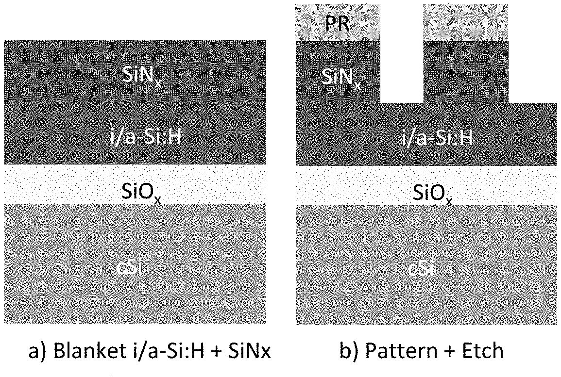
In a first embodiment, a deposited mask is used to form a layer of heavily doped amorphous silicon with alternating doping types. As shown in FIG. 1A, the method begins with a structure that includes a crystalline silicon (cSi) substrate on which a silicon oxide (SiO.sub.x) layer that serves as a tunneling oxide layer is formed. The SiO.sub.x layer may have a thickness of approximately 1.5 nm, and may be grown thermally at a temperature of 700.degree. C. Plasma-assisted chemical vapor deposition (PECVD) may be used to perform the various deposition steps discussed below.
In a first step shown in FIG. 1A, an intrinsic amorphous hydrogenated silicon (i/a-Si:H) layer is deposited on the SiO.sub.x layer. The i/a-Si:H layer may have a thickness of at least 20 nm. This layer is then covered with a deposited film such as silicon nitride (SiN.sub.x), Al.sub.2O.sub.3, SiO.sub.x, or combinations thereof. The deposited film is shown in FIG. 1A as a first SiN.sub.x layer. In a second step shown in FIG. 1B, a first photoresist (PR) is patterned via any suitable lithographic technique on a portion of the first SiN.sub.x layer. The exposed portion of the first SiN.sub.x layer is etched via wet chemistry such as dilute hydrofluoric acid (HF), and the PR is subsequently removed by a solvent such as acetone.
In a third step shown in FIG. 1C, the first PR is completely removed, and a p-type amorphous hydrogenated silicon (p/a-Si:H) layer is deposited on the structure, where portions of the p/a-Si:H layer are in direct contact with the i/a-Si:H layer. The p/a-Si:H layer may be doped with any suitable p-type dopant, such as B. The p/a-Si:H layer may have a thickness of at least 5 nm, and may have a dopant concentration of approximately 10.sup.21 cm.sup.-3. A second SiN.sub.x layer is then deposited on the p/a-Si:H layer.
In a fourth step shown in FIG. 1D, a second PR is patterned on portions of the second SiN.sub.x layer to protect the part of the underlying p/a-Si:H layer that is in direct contact with the i/a-Si:H layer. In a fifth step shown in FIG. 1E, portions of the second SiN.sub.x layer, the p/a-Si:H layer, and the first SiN.sub.x layer that are not covered by the second PR are etched by any suitable method, such as exposing the structure to reactive ion etching (RIE) or wet chemistry (HF). The second PR is then removed.
In a sixth step shown in FIG. 1F, an n-type amorphous hydrogenated silicon (n/a-Si:H) layer is deposited on the structure, and a third SiN.sub.x layer is formed on the n/a-Si:H layer. The n/a-Si:H layer may be doped with any suitable n-type dopant, such as P. The n/a-Si:H layer may have a thickness of at least 5 nm, and may have a dopant concentration of approximately 10.sup.21 cm.sup.-3. In a seventh step shown in FIG. 1G, a third PR is patterned on portions of the third SiN.sub.x layer to protect the part of the underlying n/a-Si:H layer that is in direct contact with the i/a-Si:H layer. In an eighth step shown in FIG. 1H, the portions of the third SiN.sub.x layer and the n/a-Si:H layer that are not covered by the third PR are etched by any suitable method, such as exposing the structure to reactive ion etching (RIE) or wet chemistry (HF). The third PR is then removed.
In a ninth step shown in FIG. 1I, the remaining sections of the second and third SiN.sub.x layers are removed by any suitable method, such as etching with HF. In a tenth step shown in FIG. 1J, the structure is annealed at high temperatures, such as greater than 650.degree. C., which effuses hydrogen and causes dopants from the n/a-Si:H and p/a-Si:H regions to diffuse into the i/a-Si:H layer, while all of the remaining layers in the structure (except for the SiO.sub.x and cSi layers) crystallize into polysilicon. This forms alternating regions of n-type polycrystalline silicon (n/polySi) and p-type polycrystalline silicon (p/polySi). The n-type and p-type regions may have the same or different widths. The SiO.sub.x layer allows for the high temperatures that are used during annealing to drive the dopants into the i/a-Si:H layer.
The deposited mask approach of the first embodiment may be modified in various ways. For example, as shown in FIGS. 2A through 2J, additional masking layers may be formed on the SiN.sub.x layers. The selection of the material for the masking layers is subject to the desired chemistries to be used to etch, since etching selectivity is material dependent. For example, photoresist does not etch with RIE, while a-Si:H does etch with RIE. Similarly, a-Si:H does not etch with HF, while SiN.sub.x, Al.sub.2O.sub.3, and SiO.sub.x do etch with HF. The additional masking layers shown in FIG. 2 are intrinsic amorphous silicon (i/a-Si:H) layers. The steps performed in FIGS. 2A-2J may be the same as the steps described above with regard to FIGS. 1A-1J, respectively.
Further, as shown in FIGS. 3A-3H, the patterning of the doped layers may be modified to provide an undoped gap between adjacent doped layers. For example, the second PR that is deposited in the fourth step shown in FIG. 3D may be widened, such that portions of the first SiN.sub.x layer and the additional masking layer remain. The third PR is used as a mask in the seventh step shown in FIG. 3G, such that after the portions are etched away during the eighth step shown in FIG. 3H, a space is formed between the n/a-Si:H and p/a-Si:H regions. In the tenth step shown in FIG. 3J, the structure is annealed at high temperatures, such as greater than 650.degree. C., which effuses hydrogen and causes dopants from the n/a-Si:H and p/a-Si:H regions to diffuse into the i/a-Si:H layer, while the n/a-Si:H, p/a-Si:H, and i/a-Si:H layers crystallize into polysilicon. This forms alternating regions of n-type polycrystalline silicon (n/polySi), intrinsic polycrystalline silicon (i/polySi), and p-type polycrystalline silicon (p/polySi). The steps performed in FIGS. 3A-3J may be the same as the steps described above with regard to FIGS. 1A-1J, respectively.
In a second embodiment, a shadow mask is used to form a layer of heavily doped amorphous silicon with alternating doping types. For example, the shadow mask may be made of a perforated metal sheet or a Si wafer that is patterned by laser-initiated etching. As shown in FIG. 4A, the method begins with a structure that includes a crystalline silicon (cSi) substrate on which a silicon oxide (SiO.sub.x) layer that serves as a tunneling oxide layer is formed. The SiO.sub.x layer may have a thickness of approximately 1.5 nm, and may be grown thermally at a temperature of 700.degree. C. PECVD may be used to perform the various deposition steps discussed below.
In a first step shown in FIG. 4A, an intrinsic amorphous hydrogenated silicon (i/a-Si:H) layer is deposited on the SiO.sub.x layer. The i/a-Si:H layer may have a thickness of at least 20 nm. In a second step shown in FIG. 4B, a first shadow mask (n/shadowmask) is used to deposit an n-type amorphous hydrogenated silicon (n/a-Si:H) layer on regions of the i/a-Si:H layer. The n/a-Si:H layer may be doped with any suitable n-type dopant, such as P. The n/a-Si:H layer may have a thickness of at least 5 nm, and may have a dopant concentration of approximately 10.sup.21 cm.sup.-3. In a third step shown in FIG. 4C, a second shadow mask (p/shadowmask) is used to deposit a p-type amorphous hydrogenated silicon (p/a-Si:H) layer on other regions of the i/a-Si:H layer. The p/a-Si:H layer may be doped with any suitable p-type dopant, such as B. The p/a-Si:H layer may have a thickness of at least 5 nm, and may have a dopant concentration of approximately 10.sup.21 cm.sup.-3. The p/a-Si:H regions alternate with the n/a-Si:H regions, and spaces having a width between approximately 50 .mu.m and approximately 100 .mu.m may be formed between adjacent p/a-Si:H and n/a-Si:H regions. Although the shadow masks are shown as being spaced apart from the i/a-Si:H layer in FIGS. 4B and 4C, the shadow masks may be in direct contact with the i/a-Si:H layer during deposition. The shadow masks may provide an edge roughness and pattern fidelity of approximately 10 .mu.m.
In a fourth step shown in FIG. 4D, the structure is annealed at high temperatures, such as greater than 650.degree. C., which effuses hydrogen and causes dopants from the n/a-Si:H and p/a-Si:H regions to diffuse into the i/a-Si:H layer, while the n/a-Si:H, p/a-Si:H, and i/a-Si:H layers crystallize into polysilicon. This forms alternating regions of n-type polycrystalline silicon (n/polySi), intrinsic polycrystalline silicon (i/polySi), and p-type polycrystalline silicon (p/polySi). The n-type and p-type regions may have the same or different widths. The SiO.sub.x layer allows for the high temperatures that are used during annealing to drive the dopants into the i/a-Si:H layer.
In both embodiments, the resulting structure may then receive an atomic layer deposited (ALD) Al.sub.2O.sub.3 layer with an additional SiN.sub.x layer deposited by PECVD on the textured front surface. A subsequent forming gas anneal (FGA) at approximately 400.degree. C. may further passivate the structure by hydrogenation and field effects. After removal of the sacrificial Al.sub.2O.sub.3 layer from the back, the IBC structure may be metallized by thermal evaporated Al through a Si wafer shadow mask or a lithographically defined patterned photoresist. The emitter and back surface field (BSF) contacts, as well as the intrinsic poly-Si gap layers, may be optimized separately using symmetric test structures. These may be deposited on planarized and tunnel-oxidized n-Cz wafers.
To test the methods discussed above, symmetric lifetime structures were grown and measured. Before depositing doped source layers for n- and p-type passivated contacts, intrinsic poly-Si/SiO.sub.2 structures with high surface passivation were developed. These underwent the same thermal treatments and passivation by ALD Al.sub.2O.sub.3 as the sandwich-doped layers. The best degree of passivation of i/poly-Si/SiO.sub.2 was obtained using a high hydrogen dilution H.sub.2/SiH.sub.4 ratio during PECVD deposition of i/a-Si:H at a low rate less than 0.5 .ANG./s. Other factors are the deposition temperature and the i/a-Si:H film thickness, as summarized in FIG. 5. Thicker a-Si:H layers produce better surface passivation but develop blisters during 850.degree. C. annealing. These do not affect the implied open-circuit voltage (iV.sub.oc) initially but cause performance loss upon further cell processing. In contrast, depositing a-Si:H at a temperature greater than 400.degree. C. already produces films with blisters (see inset of FIG. 5A), resulting in a low iV.sub.oc.
After selecting the i/poly-Si process with a 20 nm thick film deposited at 300.degree. C. under optimal PECVD conditions, heavily doped n-type or p-type a-Si:H was deposited. The dopants were then driven into the rest of the poly-Si by thermal diffusion, with a goal of producing the average dopant concentrations within poly-Si of approximately 2.times.10.sup.20 cm.sup.-3. As seen from FIG. 6, high performance p-type and n-type passivated contacts can be produced by this method. Notably, the typically more problematic p-type passivated contacts exhibit an iV.sub.oc over 700 mV after this processing. This might be associated with less accumulation of B into the tunneling oxide after diffusion through the poly-Si layer. The n-type contact has a remarkably high iV.sub.oc after annealing at 650.degree. C. but deteriorates with increasing the annealing temperature. This is somewhat unexpected since uniformly doped n-type contacts after annealing at 850.degree. C. and passivation typically show an iV.sub.oc greater than 730 mV peaking near the 850.degree. C. anneal temperature. The above effect might be due to an overall amount of P that is too low, leading to a reduced field effect passivation.
In-plane 2D spatial patterning of B and P dopants was also investigated. For this purpose, dopant-source layers shown in FIG. 6A were deposited by spatially-masked PECVD using (i) a mechanical mask as described above with regard to the second embodiment and (ii) photolithographically patterned, sacrificial dielectric layers on top of the blanket intrinsic a-Si:H as described above with regard to the first embodiment.
To ensure the absence of edge effects during PECVD, patterned Si wafers were used as shadow masks for the dopant source overlayers in an example based on the second embodiment. FIG. 7A shows the resulting pattern of an approximately 10 nm thick a-Si:H layer deposited on quartz through the n-type finger (BSF) mask of the 2.times.2 cm.sup.2 IBC cell. In this example, the a-Si:H finger edge fidelity was approximately 17 measured as the exponential decay length of the optical microreflectance scan (FIG. 7B). Taking into account that the poly-Si resistivity increases highly nonlinearly with doping below 10.sup.19 cm.sup.-3, this suggests that the 100 .mu.m wide intrinsic poly-Si gap will remain insulating between the n-type and p-type fingers. This is important because the weak shuntage criterion for an IBC cell (R.sub.shunt/R.sub.char>100) holds only if the sheet resistivity of the i/poly-Si gap is on the order of MS.OMEGA./.quadrature., as the total gap length even in a 2.times.2 cm.sup.2 cell is about 80 cm. Note that unlike the diffused IBC cells, the poly-Si contact based IBC cell is easily shunted due to the ohmic behavior of junctions between heavily doped and defective i-type, n-type, and p-type poly-Si layers.
Patterning dopant source layers was also done using dielectric layers to protect intrinsic a-Si:H during doped a-Si:H PECVD, with lithography steps in between n-type and p-type depositions in an example based on the first embodiment. As shown in FIG. 8, this technique provides excellent edge fidelity. However, this process is more complex than the high-throughput mechanical masking of the second embodiment.
The foregoing disclosure has been set forth merely to illustrate the invention and is not intended to be limiting. Since modifications of the disclosed embodiments incorporating the spirit and substance of the invention may occur to persons skilled in the art, the invention should be construed to include everything within the scope of the appended claims and equivalents thereof.
* * * * *
References
D00000
D00001
D00002
D00003
D00004
D00005
D00006
D00007
D00008
XML
uspto.report is an independent third-party trademark research tool that is not affiliated, endorsed, or sponsored by the United States Patent and Trademark Office (USPTO) or any other governmental organization. The information provided by uspto.report is based on publicly available data at the time of writing and is intended for informational purposes only.
While we strive to provide accurate and up-to-date information, we do not guarantee the accuracy, completeness, reliability, or suitability of the information displayed on this site. The use of this site is at your own risk. Any reliance you place on such information is therefore strictly at your own risk.
All official trademark data, including owner information, should be verified by visiting the official USPTO website at www.uspto.gov. This site is not intended to replace professional legal advice and should not be used as a substitute for consulting with a legal professional who is knowledgeable about trademark law.