Electronic device
Shen , et al.
U.S. patent number 10,658,769 [Application Number 16/411,150] was granted by the patent office on 2020-05-19 for electronic device. This patent grant is currently assigned to Qisda Corporation. The grantee listed for this patent is QISDA CORPORATION. Invention is credited to Chi-Jen Chen, Min-Wen Hong, Chun-Ming Shen.


| United States Patent | 10,658,769 |
| Shen , et al. | May 19, 2020 |
Electronic device
Abstract
An electronic device includes a casing, a circuit board, an electronic component and a fixing member. The casing includes a fixing pillar and at least one rib. The rib is connected to a periphery of the fixing pillar. The circuit board includes a through hole. The fixing pillar is disposed in the through hole. The circuit board abuts against a second top surface of the rib. A thickness of the circuit board is smaller than a height between a first top surface of the fixing pillar and the second top surface of the rib. The electronic component includes a first metal member. A first ground end of the first metal member is disposed on the first top surface of the fixing pillar. A gap exists between the first ground end and the circuit board. The fixing member fixes the first ground end to the fixing pillar.
| Inventors: | Shen; Chun-Ming (Taipei, TW), Chen; Chi-Jen (Taoyuan, TW), Hong; Min-Wen (Tainan, TW) | ||||||||||
|---|---|---|---|---|---|---|---|---|---|---|---|
| Applicant: |
|
||||||||||
| Assignee: | Qisda Corporation (Taoyuan,
TW) |
||||||||||
| Family ID: | 66189139 | ||||||||||
| Appl. No.: | 16/411,150 | ||||||||||
| Filed: | May 14, 2019 |
Foreign Application Priority Data
| Dec 25, 2018 [CN] | 2018 1 1587162 | |||
| Current U.S. Class: | 1/1 |
| Current CPC Class: | H01R 4/64 (20130101); H05K 5/0247 (20130101); G03B 21/145 (20130101); H05K 5/006 (20130101) |
| Current International Class: | H01R 4/64 (20060101); G03B 21/14 (20060101); H05K 5/00 (20060101); H05K 5/02 (20060101) |
| Field of Search: | ;439/97,95,76.1,607.35-607.4 |
References Cited [Referenced By]
U.S. Patent Documents
| 4927367 | May 1990 | Salvagno |
| 5563770 | October 1996 | Bethurum |
| 6053771 | April 2000 | Hood, III |
| 7094076 | August 2006 | Hatakeyama |
| 7326063 | February 2008 | Raudenbush |
| 9769955 | September 2017 | Teraki |
| 2002/0164895 | November 2002 | Hartke |
| 2003/0156400 | August 2003 | Dibene, II |
| 2006/0223347 | October 2006 | Kim |
| 2007/0237348 | October 2007 | Phillips |
| 2009/0268416 | October 2009 | Kanda |
| 2014/0256180 | September 2014 | Xiao |
Claims
What is claimed is:
1. An electronic device comprising: a casing comprising a fixing pillar and at least one rib, the at least one rib being connected to a periphery of the fixing pillar, a first top surface of the fixing pillar protruding from a second top surface of the at least one rib with a height; a circuit board comprising a through hole, the fixing pillar being disposed in the through hole, the circuit board abutting against the second top surface of the at least one rib, a thickness of the circuit board being smaller than the height; an electronic component disposed on the casing, the electronic component comprising a first metal member, a first ground end of the first metal member being disposed on the first top surface of the fixing pillar, a gap existing between the first ground end and the circuit board; and a fixing member fixing the first ground end to the fixing pillar.
2. The electronic device of claim 1, further comprising a second metal member disposed in the casing, a second ground end of the second metal member being disposed on the first ground end, the fixing member fixing the second ground end and the first ground end to the fixing pillar.
3. The electronic device of claim 2, wherein a first contact surface of the first ground end contacts a second contact surface of the second ground end, and at least one of the first contact surface and the second contact surface is uneven.
4. The electronic device of claim 1, wherein the electronic component is a socket.
Description
BACKGROUND OF THE INVENTION
1. Field of the Invention
The invention relates to an electronic device and, more particularly, to an electronic device capable of grounding an electronic component effectively.
2. Description of the Prior Art
At present, a power socket is disposed on a circuit board in lots of electronic devices and used to connect a power cable. In general, the power socket has a ground wire and the ground wire is fixed to a ground screw hole of an iron member to forma ground loop. To prevent the ground wire from contacting the circuit board, two fixing holes have to be formed on the circuit board, wherein one fixing hole is used to ensure safety ground for the power socket and the other fixing hole is used to fix the circuit board. Accordingly, the grounding manner of the prior art is inefficient and the manufacture cost will increase.
SUMMARY OF THE INVENTION
An objective of the invention is to provide an electronic device capable of grounding an electronic component effectively, so as to solve the aforesaid problems.
According to an embodiment of the invention, an electronic device comprises a casing, a circuit board, an electronic component and a fixing member. The casing comprises a fixing pillar and at least one rib. The at least one rib is connected to a periphery of the fixing pillar. A first top surface of the fixing pillar protrudes from a second top surface of the at least one rib with a height. The circuit board comprises a through hole. The fixing pillar is disposed in the through hole. The circuit board abuts against the second top surface of the at least one rib. A thickness of the circuit board is smaller than the height between the first top surface of the fixing pillar and the second top surface of the at least one rib. The electronic component is disposed on the casing. The electronic component comprises a first metal member. A first ground end of the first metal member is disposed on the first top surface of the fixing pillar. A gap exists between the first ground end and the circuit board. The fixing member fixes the first ground end to the fixing pillar.
As mentioned in the above, the invention uses the fixing member to fix the first ground end of the first metal member of the electronic component to the fixing pillar of the casing, so as to form a ground loop. Since the first top surface of the fixing pillar protrudes from the second top surface of the rib with a height and the thickness of the circuit board is smaller than the height, a gap exists between the first ground end of the first metal member and the circuit board (i.e. the first ground end of the first metal member does not contact the circuit board) when the circuit board abuts against the second top surface of the rib. Accordingly, the invention can ensure safety ground for the electronic component, so as to conform to the requirement of safety test. Furthermore, the invention does not need additional ground wire, so the assembly process is efficient and the manufacture cost can decrease.
These and other objectives of the present invention will no doubt become obvious to those of ordinary skill in the art after reading the following detailed description of the preferred embodiment that is illustrated in the various figures and drawings.
BRIEF DESCRIPTION OF THE DRAWINGS
FIG. 1 is a perspective view illustrating an electronic device according to an embodiment of the invention.
FIG. 2 is a partial inner view illustrating the electronic device shown in FIG. 1.
FIG. 3 is an exploded view illustrating the electronic device shown in FIG. 2.
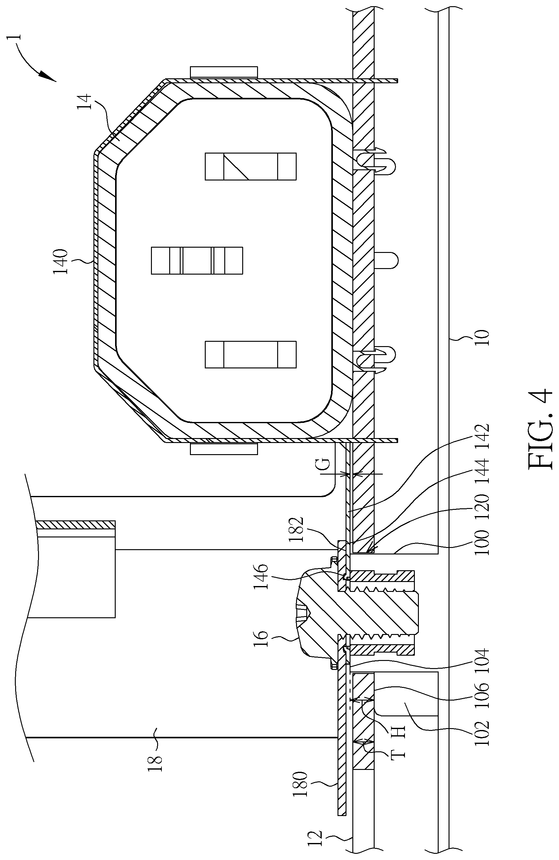
FIG. 4 is a partial sectional view illustrating the electronic device shown in FIG. 2 along line X-X.
DETAILED DESCRIPTION
Referring to FIGS. 1 to 4, FIG. 1 is a perspective view illustrating an electronic device 1 according to an embodiment of the invention, FIG. 2 is a partial inner view illustrating the electronic device 1 shown in FIG. 1, FIG. 3 is an exploded view illustrating the electronic device 1 shown in FIG. 2, and FIG. 4 is a partial sectional view illustrating the electronic device 1 shown in FIG. 2 along line X-X.
As shown in FIGS. 1 to 4, the electronic device 1 comprises a casing 10, a circuit board 12, an electronic component 14, a fixing member 16 and a second metal member 18. In this embodiment, the electronic device 1 may be, but not limited to, a projector and the electronic component 14 may be, but not limited to, a socket. In general, the electronic device 1 may be further equipped with some necessary hardware or software components for specific purposes, such as a memory, an input/output port, applications, a power supply, a communication module, etc., and it depends on practical applications.
As shown in FIG. 3, the casing 10 comprises a fixing pillar 100 and at least one rib 102, wherein the at least one rib 102 is connected to a periphery of the fixing pillar 100. In this embodiment, three ribs 102 are connected to the periphery of the fixing pillar 100 to reinforce structural strength of the fixing pillar 100. It should be noted that the number of the ribs 102 may be determined according to practical applications, so the invention is not limited to the embodiment shown in the figures. A first top surface 104 of the fixing pillar 100 protrudes from a second top surface 106 of the rib 102 with a height H. The circuit board 12 comprises a through hole 120 and a thickness T of the circuit board 12 is smaller than the height H between the first top surface 104 of the fixing pillar 100 and the second top surface 106 of the rib 102. The electronic component 14 comprises a first metal member 140.
To assemble the circuit board 12, the electronic component 14 and the second metal member 18 to the casing 10, an operator may dispose the fixing pillar 100 of the casing 10 in the through hole 120 of the circuit board 12 first, such that the circuit board 12 abuts against the second top surface 106 of the rib 102. Then, the operator may dispose the electronic component 14 on the casing 10 and dispose a first ground end 142 of the first metal member 140 on the first top surface 104 of the fixing pillar 100. Then, the operator may dispose the second metal member 18 in the casing 10 and dispose a second ground end 180 of the second metal member 18 on the first ground end 142 of the first metal member 140. Then, the operator may use the fixing member 16 to fix the second ground end 180 of the second metal member 18 and the first ground end 142 of the first metal member 140 to the fixing pillar 100. In this embodiment, the fixing member 16 may be a screw and the fixing pillar 100 may has a screw hole for fixing the screw.
Since the thickness T of the circuit board 12 is smaller than the height H between the first top surface 104 of the fixing pillar 100 and the second top surface 106 of the rib 102, a gap G (as shown in FIG. 4) exists between the first ground end 142 of the first metal member 140 and the circuit board 12 (i.e. the first ground end 142 of the first metal member 140 does not contact the circuit board 12) when the circuit board 12 abuts against the second top surface 106 of the rib 102. Accordingly, the invention can ensure safety ground for the electronic component 14, so as to conform to the requirement of safety test.
In this embodiment, the invention may adjust the dimension of the gap G by adjusting the height H between the first top surface 104 of the fixing pillar 100 and the second top surface 106 of the rib 102. Furthermore, the dimension of the gap G may be determined according to practical safety regulation. For example, the gap G must be larger than 0.1 mm for safety regulation IEC 62368.
As shown in FIG. 4, after the assembly process, a first contact surface 144 of the first ground end 142 of the first metal member 140 contacts a second contact surface 182 of the second ground end 180 of the second metal member 18. In this embodiment, the first contact surface 144 may have a plurality of protrusions 146, such that the first contact surface 144 is uneven. Accordingly, after the fixing member 16 fixes the second ground end 180 of the second metal member 18 and the first ground end 142 of the first metal member 140 to the fixing pillar 100, the invention can ensure that the first contact surface 144 and the second contact surface 182 contact with each other tightly. It should be noted that in addition to the aforesaid protrusion 146, the first contact surface 144 may also be formed as a wavy structure, a saw-toothed structure or other uneven structures according to practical applications. In another embodiment, the second contact surface 182 may also be uneven. That is to say, at least one of the first contact surface 144 and the second contact surface 182 may be uneven, so as to ensure that the first contact surface 144 and the second contact surface 182 contact with each other tightly.
As mentioned in the above, the invention uses the fixing member to fix the first ground end of the first metal member of the electronic component to the fixing pillar of the casing, so as to form a ground loop. Since the first top surface of the fixing pillar protrudes from the second top surface of the rib with a height and the thickness of the circuit board is smaller than the height, a gap exists between the first ground end of the first metal member and the circuit board (i.e. the first ground end of the first metal member does not contact the circuit board) when the circuit board abuts against the second top surface of the rib. Accordingly, the invention can ensure safety ground for the electronic component, so as to conform to the requirement of safety test. Furthermore, the invention does not need additional ground wire, so the assembly process is efficient and the manufacture cost can decrease.
Those skilled in the art will readily observe that numerous modifications and alterations of the device and method may be made while retaining the teachings of the invention. Accordingly, the above disclosure should be construed as limited only by the metes and bounds of the appended claims.
* * * * *
D00000
D00001
D00002
D00003
D00004
XML
uspto.report is an independent third-party trademark research tool that is not affiliated, endorsed, or sponsored by the United States Patent and Trademark Office (USPTO) or any other governmental organization. The information provided by uspto.report is based on publicly available data at the time of writing and is intended for informational purposes only.
While we strive to provide accurate and up-to-date information, we do not guarantee the accuracy, completeness, reliability, or suitability of the information displayed on this site. The use of this site is at your own risk. Any reliance you place on such information is therefore strictly at your own risk.
All official trademark data, including owner information, should be verified by visiting the official USPTO website at www.uspto.gov. This site is not intended to replace professional legal advice and should not be used as a substitute for consulting with a legal professional who is knowledgeable about trademark law.