Multiplexed Fourier ptychography imaging systems and methods
Horstmeyer , et al.
U.S. patent number 10,652,444 [Application Number 14/960,252] was granted by the patent office on 2020-05-12 for multiplexed fourier ptychography imaging systems and methods. This patent grant is currently assigned to CALIFORNIA INSTITUTE OF TECHNOLOGY. The grantee listed for this patent is California Institute of Technology. Invention is credited to Roarke W. Horstmeyer, Changhuei Yang, Guoan Zheng.


View All Diagrams
| United States Patent | 10,652,444 |
| Horstmeyer , et al. | May 12, 2020 |
Multiplexed Fourier ptychography imaging systems and methods
Abstract
Certain embodiments pertain to Multiplexed Fourier Ptychographic imaging systems and methods. In one example, the Multiplexed Fourier Ptychographic imaging system includes an LED array configured to illuminate a sequence of LED patterns for illuminating a sample being imaged. The system includes LED circuitry configured to independently control power to turn on multiple LEDs simultaneously in each LED pattern of the array. The system has a light detector that acquires a first set of lower resolution images of the sample each image acquired during exposure time during illumination by a unique LED pattern. The system uses the first set of lower resolution images to generate a second set of lower resolution images associated with each LED in the LED array and iteratively updates overlapping regions in the Fourier domain with the second set of lower resolution images to generate a higher resolution image.
| Inventors: | Horstmeyer; Roarke W. (San Marino, CA), Zheng; Guoan (Vernon, CT), Yang; Changhuei (Alhambra, CA) | ||||||||||
|---|---|---|---|---|---|---|---|---|---|---|---|
| Applicant: |
|
||||||||||
| Assignee: | CALIFORNIA INSTITUTE OF
TECHNOLOGY (Pasadena, CA) |
||||||||||
| Family ID: | 55526968 | ||||||||||
| Appl. No.: | 14/960,252 | ||||||||||
| Filed: | December 4, 2015 |
Prior Publication Data
| Document Identifier | Publication Date | |
|---|---|---|
| US 20160088205 A1 | Mar 24, 2016 | |
Related U.S. Patent Documents
| Application Number | Filing Date | Patent Number | Issue Date | ||
|---|---|---|---|---|---|
| 14065280 | Oct 28, 2013 | ||||
| 61720258 | Oct 30, 2012 | ||||
| 61847472 | Jul 17, 2013 | ||||
| 62087633 | Dec 4, 2014 | ||||
| Current U.S. Class: | 1/1 |
| Current CPC Class: | G02B 21/365 (20130101); H04N 5/23229 (20130101); G02B 21/367 (20130101); H04N 5/2256 (20130101); H04N 5/265 (20130101); G02B 27/58 (20130101); G06K 9/00134 (20130101); G21K 7/00 (20130101); G02B 21/002 (20130101) |
| Current International Class: | G02B 21/00 (20060101); H04N 5/225 (20060101); H04N 5/232 (20060101); H04N 5/265 (20060101); G02B 27/58 (20060101); G06K 9/00 (20060101); G02B 21/36 (20060101); G21K 7/00 (20060101) |
| Field of Search: | ;356/445 ;359/385 ;204/452 ;250/208.1 ;348/80 |
References Cited [Referenced By]
U.S. Patent Documents
| 5475527 | December 1995 | Hackel et al. |
| 6144365 | November 2000 | Young et al. |
| 6154196 | November 2000 | Fleck et al. |
| 6320174 | November 2001 | Tafas et al. |
| 6320648 | November 2001 | Brueck et al. |
| 6747781 | June 2004 | Trisnadi |
| 6759949 | July 2004 | Miyahara |
| 6905838 | June 2005 | Bittner |
| 7436503 | October 2008 | Chen et al. |
| 7460248 | December 2008 | Kurtz et al. |
| 7706419 | April 2010 | Wang et al. |
| 7738095 | June 2010 | Gardner, Jr. et al. |
| 7787588 | August 2010 | Yun et al. |
| 8271251 | September 2012 | Schwartz et al. |
| 8313031 | November 2012 | Vinogradov |
| 8497934 | July 2013 | Milnes et al. |
| 8624968 | January 2014 | Zheng et al. |
| 8654201 | February 2014 | Lim et al. |
| 8942449 | January 2015 | Maiden |
| 9029745 | May 2015 | Maiden |
| 9426455 | August 2016 | Horstmeyer et al. |
| 9497379 | November 2016 | Ou et al. |
| 9829695 | November 2017 | Kim et al. |
| 9864184 | January 2018 | Ou et al. |
| 9892812 | February 2018 | Zheng et al. |
| 9983397 | May 2018 | Horstmeyer et al. |
| 9993149 | June 2018 | Chung et al. |
| 9998658 | June 2018 | Ou et al. |
| 10162161 | December 2018 | Horstmeyer et al. |
| 10168525 | January 2019 | Kim et al. |
| 10222605 | March 2019 | Kim et al. |
| 10228550 | March 2019 | Ou et al. |
| 10401609 | September 2019 | Ou et al. |
| 10419665 | September 2019 | Ou et al. |
| 10568507 | February 2020 | Chung et al. |
| 2001/0055062 | December 2001 | Shioda et al. |
| 2002/0141051 | October 2002 | Vogt et al. |
| 2003/0116436 | June 2003 | Amirkhanian |
| 2003/0118223 | June 2003 | Rahn et al. |
| 2004/0057094 | March 2004 | Olszak et al. |
| 2004/0146196 | July 2004 | Van Heel |
| 2004/0190762 | September 2004 | Dowski, Jr. et al. |
| 2005/0211912 | September 2005 | Fox |
| 2006/0098293 | May 2006 | Garoutte et al. |
| 2006/0158754 | July 2006 | Tsukagoshi et al. |
| 2006/0173313 | August 2006 | Liu et al. |
| 2006/0291707 | December 2006 | Kothapalli et al. |
| 2007/0057184 | March 2007 | Uto et al. |
| 2007/0133113 | June 2007 | Minabe et al. |
| 2007/0159639 | July 2007 | Teramura et al. |
| 2007/0171430 | July 2007 | Tearney et al. |
| 2007/0189436 | August 2007 | Goto et al. |
| 2007/0206200 | September 2007 | Lindner et al. |
| 2007/0269826 | November 2007 | Geddes |
| 2008/0101664 | May 2008 | Perez |
| 2008/0182336 | July 2008 | Zhuang et al. |
| 2009/0046164 | February 2009 | Shroff et al. |
| 2009/0079987 | March 2009 | Ben-Ezra |
| 2009/0125242 | May 2009 | Choi et al. |
| 2009/0284831 | November 2009 | Schuster et al. |
| 2009/0316141 | December 2009 | Feldkhun |
| 2010/0135547 | June 2010 | Lee et al. |
| 2010/0271705 | October 2010 | Hung |
| 2011/0075928 | March 2011 | Jeong et al. |
| 2011/0181869 | July 2011 | Yamaguchi et al. |
| 2011/0192976 | August 2011 | Own et al. |
| 2011/0235863 | September 2011 | Maiden |
| 2011/0255163 | October 2011 | Merrill et al. |
| 2012/0069344 | March 2012 | Liu |
| 2012/0099803 | April 2012 | Ozcan et al. |
| 2012/0105618 | May 2012 | Brueck et al. |
| 2012/0118967 | May 2012 | Gerst |
| 2012/0157160 | June 2012 | Ozcan et al. |
| 2012/0176673 | July 2012 | Cooper |
| 2012/0182541 | July 2012 | Canham |
| 2012/0218379 | August 2012 | Ozcan et al. |
| 2012/0248292 | October 2012 | Ozcan |
| 2012/0250032 | October 2012 | Wilde et al. |
| 2012/0281929 | November 2012 | Brand et al. |
| 2013/0057748 | March 2013 | Duparre et al. |
| 2013/0083886 | April 2013 | Carmi et al. |
| 2013/0093871 | April 2013 | Nowatzyk et al. |
| 2013/0094077 | April 2013 | Brueck |
| 2013/0100525 | April 2013 | Chiang et al. |
| 2013/0170767 | July 2013 | Choudhury et al. |
| 2013/0182096 | July 2013 | Boccara et al. |
| 2013/0223685 | August 2013 | Maiden |
| 2014/0007307 | January 2014 | Routh, Jr. et al. |
| 2014/0029824 | January 2014 | Shi et al. |
| 2014/0043616 | February 2014 | Maiden et al. |
| 2014/0050382 | February 2014 | Adie et al. |
| 2014/0085629 | March 2014 | Bodkin et al. |
| 2014/0118529 | May 2014 | Zheng et al. |
| 2014/0126691 | May 2014 | Zheng et al. |
| 2014/0133702 | May 2014 | Zheng et al. |
| 2014/0152801 | June 2014 | Fine et al. |
| 2014/0153692 | June 2014 | Larkin et al. |
| 2014/0160236 | June 2014 | Ozcan et al. |
| 2014/0160488 | June 2014 | Zhou |
| 2014/0217268 | August 2014 | Schleipen et al. |
| 2014/0267674 | September 2014 | Mertz et al. |
| 2014/0347672 | November 2014 | Pavillon et al. |
| 2014/0368812 | December 2014 | Humphry et al. |
| 2015/0036038 | February 2015 | Horstmeyer et al. |
| 2015/0044098 | February 2015 | Smart et al. |
| 2015/0054979 | February 2015 | Ou et al. |
| 2015/0160450 | June 2015 | Ou et al. |
| 2015/0264250 | September 2015 | Ou et al. |
| 2015/0286042 | October 2015 | Hilbert et al. |
| 2015/0331228 | November 2015 | Horstmeyer et al. |
| 2016/0110584 | April 2016 | Remiszewski et al. |
| 2016/0156880 | June 2016 | Teich et al. |
| 2016/0178883 | June 2016 | Horstmeyer et al. |
| 2016/0202460 | July 2016 | Zheng |
| 2016/0210763 | July 2016 | Horstmeyer et al. |
| 2016/0216208 | July 2016 | Kim et al. |
| 2016/0216503 | July 2016 | Kim et al. |
| 2016/0266366 | September 2016 | Chung et al. |
| 2016/0320595 | November 2016 | Horstmeyer et al. |
| 2016/0320605 | November 2016 | Ou et al. |
| 2016/0341945 | November 2016 | Ou et al. |
| 2017/0061599 | March 2017 | Remiszewski et al. |
| 2017/0146788 | May 2017 | Waller et al. |
| 2017/0178317 | June 2017 | Besley et al. |
| 2017/0188853 | July 2017 | Nakao et al. |
| 2017/0273551 | September 2017 | Chung et al. |
| 2017/0299854 | October 2017 | Kim et al. |
| 2017/0354329 | December 2017 | Chung et al. |
| 2017/0363853 | December 2017 | Besley |
| 2017/0371141 | December 2017 | Besley |
| 2018/0045569 | February 2018 | Nath et al. |
| 2018/0048811 | February 2018 | Waller et al. |
| 2018/0078447 | March 2018 | Viner et al. |
| 2018/0078448 | March 2018 | Shockley, Jr. et al. |
| 2018/0088309 | March 2018 | Ou et al. |
| 2018/0120553 | May 2018 | Leshem et al. |
| 2018/0231761 | August 2018 | Dai et al. |
| 2018/0307017 | October 2018 | Horstmeyer et al. |
| 2018/0316855 | November 2018 | Ou et al. |
| 2018/0329194 | November 2018 | Small et al. |
| 2018/0348500 | December 2018 | Naaman, III et al. |
| 2018/0373016 | December 2018 | Leshem et al. |
| 2019/0049712 | February 2019 | Kim et al. |
| 2019/0056578 | February 2019 | Horstmeyer et al. |
| 2019/0077610 | March 2019 | Flammann |
| 2019/0097523 | March 2019 | Schaefer |
| 2019/0097524 | March 2019 | Lin |
| 2019/0137753 | May 2019 | Chan et al. |
| 2019/0317311 | October 2019 | Kim et al. |
| 2019/0331902 | October 2019 | Ou et al. |
| 2019/0391382 | December 2019 | Chung et al. |
| 1688254 | Oct 2005 | CN | |||
| 1932565 | Mar 2007 | CN | |||
| 1311392 | Apr 2007 | CN | |||
| 101408623 | Apr 2009 | CN | |||
| 101680848 | Mar 2010 | CN | |||
| 101743519 | Jun 2010 | CN | |||
| 101868740 | Oct 2010 | CN | |||
| 101872033 | Oct 2010 | CN | |||
| 101957183 | Jan 2011 | CN | |||
| 102608597 | Jul 2012 | CN | |||
| 102753935 | Oct 2012 | CN | |||
| 103096804 | May 2013 | CN | |||
| 103154662 | Jun 2013 | CN | |||
| 103201648 | Jul 2013 | CN | |||
| 103377746 | Oct 2013 | CN | |||
| 104181686 | Dec 2014 | CN | |||
| 104200449 | Dec 2014 | CN | |||
| 2007-299604 | Nov 2007 | JP | |||
| 2008-147629 | Jun 2008 | JP | |||
| 2010-012222 | Jan 2010 | JP | |||
| 10-1998-0075050 | Nov 1998 | KR | |||
| 201428339 | Jul 2014 | TW | |||
| WO 99/53469 | Oct 1999 | WO | |||
| WO 2002/102128 | Dec 2002 | WO | |||
| WO 2003/062744 | Jul 2003 | WO | |||
| WO 2008/116070 | Sep 2008 | WO | |||
| WO 2011/093043 | Aug 2011 | WO | |||
| WO 2012/037182 | Mar 2012 | WO | |||
| WO 2014/070656 | May 2014 | WO | |||
| WO 2015/017730 | Feb 2015 | WO | |||
| WO 2015/027188 | Feb 2015 | WO | |||
| WO 2016/090331 | Jun 2016 | WO | |||
| WO 2016/106379 | Jun 2016 | WO | |||
| WO 2016/118761 | Jul 2016 | WO | |||
| WO 2016/123156 | Aug 2016 | WO | |||
| WO 2016/123157 | Aug 2016 | WO | |||
| WO 2016/149120 | Sep 2016 | WO | |||
| WO 2016/187591 | Nov 2016 | WO | |||
| WO 2017/066198 | Apr 2017 | WO | |||
| WO 2017081539 | May 2017 | WO | |||
| WO 2017081540 | May 2017 | WO | |||
| WO 2017081542 | May 2017 | WO | |||
Other References
|
Tian, "Multiplexed coded illumination for Fourier Ptychography with an LED array microscope" (Year: 2014). cited by examiner . U.S. Appl. No. 15/007,196, filed Jan. 26, 2016 entitled "Array Level Fourier Ptychographic Imaging". cited by applicant . U.S. Appl. No. 15/007,159, filed Jan. 26, 2016 entitled "Multi-Well Fourier Ptychographic and Fluorescence Imaging". cited by applicant . U.S. Appl. No. 14/979,154, filed Dec. 22, 2015 entitled "EPI-Illumination Fourier Ptychographic Imaging for Thick Samples". cited by applicant . U.S. Appl. No. 15/003,559, filed Jan. 21, 2016 entitled "Fourier Ptychographic Tomography". cited by applicant . U.S. Appl. No. 15/068,389, filed Mar. 11, 2016 entitled "Correcting for Aberrations in Incoherent Imaging Systems Using Fourier Ptychographic Techniques". cited by applicant . U.S. Appl. No. 15/081,659, filed Mar. 25, 2016 entitled "Fourier Ptychographic Retinal Imaging Methods and Systems". cited by applicant . U.S. Office Action dated Oct. 5, 2015 in U.S. Appl. No. 14/065,305. cited by applicant . U.S. Notice of Allowance dated Dec. 4, 2015 in U.S. Appl. No. 14/065,305. cited by applicant . U.S. Notice of Allowance dated Jan. 14, 2016 in U.S. Appl. No. 14/448,850. cited by applicant . U.S. Notice of Allowance dated Jan. 22, 2016 in U.S. Appl. No. 14/466,481. cited by applicant . U.S. Notice of Allowance dated Apr. 13, 2016 in U.S. Appl. No. 14/448,850. cited by applicant . U.S. Notice of Allowance dated Apr. 22, 2016 in U.S. Appl. No. 14/466,481. cited by applicant . International Search Report and Written Opinion dated Feb. 21, 2014 in PCT/US2013/067068. cited by applicant . International Preliminary Report on Patentability dated May 14, 2015 in PCT/US2013/067068. cited by applicant . European Third-Party Observations, dated Dec. 14, 2015 in EP Application No. 13851670.3. cited by applicant . European Extended Search Report dated Mar. 31, 2016 in EP Application No. 13851670.3. cited by applicant . International Preliminary Report on Patentability dated Mar. 3, 2016 issued in PCT/US2014/052351. cited by applicant . International Search Report and Written Opinion dated Dec. 5, 2014 issued in PCT/US2014/052351. cited by applicant . International Search Report and Written Opinion dated Nov. 13, 2014 issued in PCT/US2014/049297. cited by applicant . International Preliminary Report on Patentability dated Feb. 11, 2016 issued in PCT/US2014/049297. cited by applicant . International Search Report and Written Opinion dated Feb. 22, 2016 issued in PCT/US2015/064126. cited by applicant . "About Molemap," Retrieved Oct. 23, 2015, 2 pages. [http://molemap.net.au/about-us/]. cited by applicant . Abramomwitz, M. et al, "Immersion Media," Olympus Microscopy Resource Center, 2012, 6 pp. [http://www.olympusmicro.com/primer/anatomy/immersion.html]. cited by applicant . Abramomwitz, M., et al, "Field Curvature," Olympus Microscopy Resource Center, 2012, 3 pp. [http://www.olympusmicro.com/primer/anatomy/fieldcurvature.html]. cited by applicant . "Age-Related Macular Degeneration (AMD) | National Eye Institute." [Online]. Available: https://www.nei.nih.gov/eyedata/amd#top. [Accessed: Apr. 5, 2016]. cited by applicant . Alexandrov, S., et al, "Spatial information transmission beyond a system's diffraction limit using optical spectral encoding of the spatial frequency," Journal of Optics A: Pure and Applied Optics 10, 025304 (2008). cited by applicant . Alexandrov, S.A., et al, "Synthetic Aperture Fourier holographic optical microscopy," Phys. Rev. Lett. 97, 168102 (2006). cited by applicant . Arimoto, H., et al, "Integral three-dimensional imaging with digital reconstruction," Opt. Lett. 26, 157-159 (2001). cited by applicant . Balan, R., et al, "On signal reconstruction without phase, Applied and Computational Harmonic Analysis 20," No. 3 (2006): 345-356. cited by applicant . Balan, R., et al, "Painless reconstruction from magnitudes of frame coefficients," J Fourier Anal Appl 15:488-501 (2009). cited by applicant . Bauschke, H.H., et al, "Phase retrieval, error reduction algorithm, and Fienup variants: a view from convex optimization," J Opt Soc Am A 19:1334-1345 (2002). cited by applicant . Becker, S., et al, "Templates for convex cone problems with applications to sparse signal recovery," Technical report, Department of Statistics, Stanford University, (2010), 48 Pages. cited by applicant . Betti, R., et al, "Observational study on the mitotic rate and other prognostic factors in cutaneous primary melanoma arising from naevi and from melanoma de novo," Journal of the European Academy of Dermatology and Venereology, 2014. cited by applicant . Bian, L., et al, "Fourier ptychographic reconstruction using Wirtinger flow optimization," Opt. Express 23:4856-4866 (2015). cited by applicant . Bian, Z., et al, "Adaptive system correction for robust Fourier ptychographic imaging," Optics express, 2013. 21(26): p. 32400-32410. cited by applicant . BioTek.RTM. Brochure: BioTek's Multi-Mode Microplate Reading Techonologies, 2016, 2 pp. [http://www.biotek.com]. cited by applicant . Bishara, W., et al,"Holographic pixel super-resolution in portable lensless on-chip microscopy using a fiber-optic array," Lab Chip 11(7), 1276-1279 (2011). cited by applicant . Bishara, W., et al, "Lensfree on-chip microscopy over a wide field-of-view using pixel super-resolution," Opt. Express 18(11), 11181-11191 (2010). cited by applicant . Blum, A., et al, "Clear differences in hand-held dermoscopes," JDDG: Journal der Deutschen Dermatologischen Gesellschaft, 2006, 4(12): p. 1054-1057. cited by applicant . Blum, A., et al, Dermatoskopie von Hauttumoren: Auflichtmikroskopie; Dermoskopie; digitale Bildanalyse; mit 28 Tabellen. 2003: Springer DE, Chapter 4 "Dermatoskopisch sichtbare Strukturen" p. 15-66. cited by applicant . Born, M., et al, "Principles of Optics: Electromagnetic theory of propagation, interference and diffraction of light" 7th Ed., Cambridge Univ. Press, (1999) pp. 1-31. cited by applicant . Brady, D., et al, "Multiscale gigapixel photography," Nature 486, 386-389 (2012). cited by applicant . Burer, S., et al, "A nonlinear programming algorithm for solving semidefinite programs via low-rank factorization," Math Program, Ser B 95:329-357 (2003). cited by applicant . Burer, S., et al, "Local minima and convergence in low-rank semidefinite programming. Math Program," Ser A 103:427-444 (2005). cited by applicant . Candes, E.J., et al, "Phase retrieval via matrix completion," SIAM J. Imaging Sci. 6:199-225 (2012). cited by applicant . Candes, E.J., et al, "Phase retrieval via Wirtinger flow: theory and algorithms," IEEE Trans. Info. Theory 61:1985-2007 (2015). cited by applicant . Candes, E.J., et al, "PhaseLift: exact and stable signal recovery from magnitude measurements via convex programming.," Comm Pure Appl Math 66:1241-1274 (2013). cited by applicant . Carroll, J., "Adaptive optics retinal imaging: applications for studying retinal degeneration," Arch. Ophthalmol., vol. 126, pp. 857-858, 2008. cited by applicant . Chao, W. et al, "Soft X-ray microscopy at a spatial resolution better than 15 nm," Nature Letters, vol. 435/30, Jun. 2005 pp. 1210-1213. cited by applicant . Chen, T., et al, "Polarization and phase shifting for 3D scanning of translucent objects," Proc. CVPR, (2007). cited by applicant . Chin, L., et al, "Malignant melanoma: genetics and therapeutics in the genomic era," Genes & development, 2006, 20(16): p. 2149-2182. cited by applicant . Choi, W., et al, "Tomographic phase microscopy," Nature Methods 4(9) (2007), pp. 1-3 Published Online Aug. 12, 2007. cited by applicant . Chung, J., et al, "Counting White Blood Cells from a Blood Smear Using Fourier Ptychographic Microscopy," PLoS One 10(7), e0133489 (2015). cited by applicant . Chung, J., et al, "Wide field-of-view fluorescence image deconvolution with aberration-estimation from Fourier ptychography," Feb. 1, 2016, vol. 7, No. 2, Biomedical Optics Express 352. cited by applicant . Colomb, T., et al, "Automatic procedure for aberration compensation in digital holographic microscopy and applications to specimen shape compensation," Appl. Opt. 45, 851-863 (2006). cited by applicant . De Sa, C., et al, "Global convergence of stochastic gradient descent for some non convex matrix problems," Proc. 32nd Int. Conf. Machine Learning (2015), 10 pp. cited by applicant . Debailleul, M., et al, "High-resolution three-dimensional tomographic diffractive microscopy of transparent inorganic and biological samples," Optic Letters 34 (2008). cited by applicant . Denis, L., et al, "Inline hologram reconstruction with sparsity constraints," Opt. Lett. 34, pp. 3475-3477 (2009). cited by applicant . Di, J., et al, "High resolution digital holographic microscopy with a wide field of view based on a synthetic aperture technique and use of linear CCD scanning," Appl. Opt. 47, pp. 5654-5659 (2008). cited by applicant . Dierolf, M., et al, "Ptychographic coherent diffractive imaging of weakly scattering specimens," New J. Phys. 12, 035017 (2010). cited by applicant . "Doctor Mole--Skin Cancer App," Retrieved Oct. 23, 2015, 1 page. [http://www.doctormole.com]. cited by applicant . Dong, S., et al, "FPscope: a field-portable high-resolution microscope using a cellphone lens," Biomed. Opt. Express 5(10), 3305-3310 (2014). cited by applicant . Dong, S., et al, "High-resolution fluorescence imaging via pattern-illuminated Fourier ptychography," Opt. Express 22(17), 20856-20870 (2014). cited by applicant . Dong, S., et al, "Aperture-scanning Fourier ptychography for 3D refocusing and super-resolution macroscopic imaging," pp. 13586-13599 (Jun. 2, 2014). cited by applicant . Eldar,Y.C., et al, "Sparse phase retrieval from short-time Fourier measurements," IEEE Signal Processing Letters 22, No. 5 (2015): 638-642. cited by applicant . Emile, O., et al, "Rotating polarization imaging in turbid media," Optics Letters 21(20), (1996). cited by applicant . Faulkner, H.M.L., and Rodenburg, J.M., "Error tolerance of an iterative phase retrieval algorithm for moveable illumination microscopy," Ultramicroscopy 103(2), 153-164 (2005). cited by applicant . Faulkner, H.M.L., and Rodenburg, J.M., "Movable aperture lensless transmission microscopy: a novel phase retrieval algorithm," Phys. Rev. Lett. 93, 023903 (2004). cited by applicant . Fazel, M., "Matrix rank minimization with applications," PhD Thesis (Stanford University, Palo Alto, CA). (2002). cited by applicant . Feng, P., et al, "Long-working-distance synthetic aperture Fresnel off-axis digital holography," Optics Express 17, pp. 5473-5480 (2009). cited by applicant . Fienup, J. R., "Invariant error metrics for image reconstruction," Appl. Opt. 36(32), 8352-8357 (1997). cited by applicant . Fienup, J. R., "Lensless coherent imaging by phase retrieval with an illumination pattern constraint," Opt. Express 14, 498-508 (2006). cited by applicant . Fienup, J. R., "Phase retrieval algorithms: a comparison," Appl. Opt. 21, 2758-2769 (1982). cited by applicant . Fienup, J. R., "Reconstruction of a complex-valued object from the modulus of its Fourier transform using a support constraint," J. Opt. Soc. Am. A 4, 118-123 (1987). cited by applicant . Fienup, J. R., "Reconstruction of an object from the modulus of its Fourier transform," Opt. Lett. 3, 27-29 (1978). cited by applicant . Gan, X., et al, "Image enhancement through turbid media under a microscope by use of polarization gating methods," JOSA A 16(9), (1999). cited by applicant . Gerke T.D., et al, "Aperiodic volume optics," Nature Photonics (2010), vol. 4, pp. 188-193. cited by applicant . Ghosh, A., et al, "Multiview face capture using polarized spherical gradient illumination," ACM Transactions on Graphics 30(6) (2011). cited by applicant . Godara, P., et al, "Adaptive optics retinal imaging: emerging clinical applications.," Optom. Vis. Sci., vol. 87, No. 12, pp. 930-941, Dec. 2010. cited by applicant . Goodman, J.W., "Introduction to Fourier Optics," Roberts & Company Publication, Third Edition, chapters 1-6, pp. 1-172 (2005). cited by applicant . Goodson, A.G., et al, "Comparative analysis of total body and dermatoscopic photographic monitoring of nevi in similar patient populations at risk for cutaneous melanoma," Dermatologic Surgery, 2010. 36(7): p. 1087-1098. cited by applicant . Granero, L., et al, "Synthetic aperture superresolved microscopy in digital lensless Fourier holography by time and angular multiplexing of the object information," Appl. Opt. 49, pp. 845-857 (2010). cited by applicant . Grant, M., et al, "CVX: Matlab software for disciplined convex programming," version 2.0 beta. http://cvxr.com/cvx, (Sep. 2013), 3 pages. cited by applicant . Greenbaum, A., et al, "Field-portable wide-field microscopy of dense samples using multi-height pixel super resolution based lensfree imaging," Lab Chip 12(7), 1242-1245 (2012). cited by applicant . Greenbaum, A., et al, "Increased space-bandwidth product in pixel super-resolved lensfree on-chip microscopy," Sci. Rep. 3, p. 1717 (2013). cited by applicant . Gruev, V., et al, "Dual-tier thin film polymer polarization imaging sensor," Optics Express, vol. 18, No. 18, 12 pages (2010). cited by applicant . Guizar-Sicairos, M., and Fienup, J.R.,"Phase retrieval with transverse translation diversity: a nonlinear optimization approach," Opt. Express 16, 7264-7278 (2008). cited by applicant . Gunturk, B.K., et al, "Image Restoration: Fundamentals and Advances," vol. 7, Chapter 3, pp. 63-68 (CRC Press, 2012). cited by applicant . Gustafsson, M.G.L., "Surpassing the lateral resolution limit by a factor of two using structured illumination microscopy," J. Microsc. 198, 82-87 (2000). cited by applicant . Gutzler, T., et al, "Coherent aperture-synthesis, wide-field, high-resolution holographic microscopy of biological tissue," Opt. Lett. 35, pp. 1136-1138 (2010). cited by applicant . Haigh, S. J., et al, (2009) "Atomic structure imaging beyond conventional resolution limits in the transmission electron microscope"; Physical Review Letters 103. 126101-1 126101-4. cited by applicant . Han, C., et al, "Wide Field-of-View On-Chip Talbot Fluorescence Microscopy for Longitudinal Cell Culture Monitoring from within the Incubator" Anal. Chem. 85(4), 2356-2360 (2013). cited by applicant . Hillman, T.R., et al, "High-resolution, wide-field object reconstruction with synthetic aperture Fourier holographic optical microscopy," Opt. Express 17, pp. 7873-7892 (2009). cited by applicant . Hofer, H., et al, "Dynamics of the eye's wave aberration," J. Opt. Soc. Am. A, vol. 18, No. 3, p. 497, 2001. cited by applicant . Hofer, H., et al, "Organization of the human trichromatic cone mosaic.," J. Neurosci., vol. 25, No. 42, pp. 9669-9679, Oct. 2005. cited by applicant . Hong, S-H., et al, "Three-dimensional volumetric object reconstruction using computational integral imaging," Opt. Express 12, 483-491 (2004). cited by applicant . Hoppe, W., "Diffraction in inhomogeneous primary wave fields. 1. Principle of phase determination from electron diffraction interference," Acta Crystallogr. A25, 495-501 1969. cited by applicant . Horstmeyer, R., et al, "A phase space model of Fourier ptychographic microscopy," Optics Express, 2014. 22(1): p. 338-358. cited by applicant . Horstmeyer, R., et al, "Digital pathology with fourier ptychography," Comput. Med. Imaging Graphics 42, 38-43 (2015). cited by applicant . Horstmeyer, R., et al, "Overlapped fourier coding for optical aberration removal," Manuscript in preparation, 19 pages (2014). cited by applicant . Horstmeyer, R., et al, "Solving ptychography with a convex relaxation," Physics Optics (2014) 1-8 pages. cited by applicant . Hue, F., et al, "Wave-front phase retrieval in transmission electron microscopy via ptychography," Phys. Rev. B 82, 121415 (2010). cited by applicant . Humphry, M., et al, "Ptychographic electron microscopy using high-angle dark-field scattering for sub-nanometre resolution imaging," Nat. Commun. 3, 730 (2012). cited by applicant . IncuCyte.RTM. ZOOM System, Brochure, 1-4 pp. (2016) (retrieved Feb. 25, 2016), [http://www.essenbioscience.com/media/uploads/files/8000-0333-E00-- IncuCyte_ZOOM_brochure.pdf]. cited by applicant . Jaganathan, K., et al, "Recovery of sparse 1-D signals from the magnitudes of their Fourier transform," IEEE International Symposium on Information Theory Proceedings (2012): 1473-1477. cited by applicant . Jaganathan, K., et al, "Phase retrieval with masks using convex optimization," IEEE International Symposium on Information Theory Proceedings (2015): 1655-1659. cited by applicant . Jaganathan, K., et al, "STFT Phase retrieval: uniqueness guarantees and recovery algorithms," arXiv preprint arXiv:1508.02820 (2015). cited by applicant . Joeres, S., et al, "Retinal imaging with adaptive optics scanning laser ophthalmoscopy in unexplained central ring scotoma.," Arch. Ophthalmol., vol. 126, No. 4, pp. 543-547, Apr. 2008. cited by applicant . Jung, J.H., et al, "Microfluidic-integrated laser-controlled microactuators with on-chip microscopy imaging functionality," Lab Chip 14 (19), Oct. 7, 2014, pp. 3781-3789. cited by applicant . Kay, D. B., et al, "Outer retinal structure in best vitelliform macular dystrophy.," JAMA Ophthalmol., vol. 131, pp. 1207-1215, 2013. cited by applicant . Kim, J., et al, Incubator embedded cell culture imaging system (EmSight) based on Fourier ptychographic microscopy. EmSight manuscript, Optical Society of America, 2015. cited by applicant . Kim, M., et al, "High-speed synthetic aperture microscopy for live cell imaging," Opt. Lett. 36, pp. 148-150 (2011). cited by applicant . Kirkland, A.I., et al, "Multiple beam tilt microscopy for super resolved imaging;" Japanese Society of Electron Microscopy: Journal of Electron Microscopy I: 11-22(1997), vol. 46, No. 1 1997. cited by applicant . Kirkland, A.I., et al, "Super-resolution by aperture synthesis: tilt series reconstruction in CTEM," Ultramicroscopy 57, (1995) 355-374, Received May 27, 1994, in final form Oct. 2, 1994; 1995 Elsevier Science B.V. SSDI 0304-3991(94)00191-x. cited by applicant . Kittler, H., et al, "Morphologic changes of pigmented skin lesions: a useful extension of the ABCD rule for dermatoscopy," Journal of the American Academy of Dermatology, 1999. 40(4): p. 558-562. cited by applicant . Kozak, I., "Retinal imaging using adaptive optics technology.," Saudi J. Ophthalmol. Off. J. Saudi Ophthalmol. Soc., vol. 28, No. 2, pp. 117-22, Apr. 2014. cited by applicant . Lauer, V., "New Approach to optical diffraction tomography yielding a vector equation of diffraction tomography and a novel tomography microscope," Journal of Microscopy, vol. 205, Pt 2 Feb. 2002, pp. 165-176, The Royal Microscopical Society 2001. cited by applicant . Lee, K., et al, "Synthetic Fourier transform light scattering," Optics Express 21 (2013). cited by applicant . Levoy, M., et al, "Light field microscopy," ACM Trans. Graphics 25, (2006). cited by applicant . Levoy, M., et al, "Recording and controlling the 4D light field in a microscope using microlens arrays," J. Microsc. 235 (2009). cited by applicant . Li, X., et al, "Sparse signal recovery from quadratic measurements via convex programming," SIAM Journal on Mathematical Analysis 45, No. 5 (2013): 3019-3033. cited by applicant . Lohmann, A. W., et al, "Space-bandwidth product of optical signals and systems," J. Opt. Soc. Am. A 13, pp. 470-473 (1996). cited by applicant . Lue, N., et al, "Live Cell Refractometry Using Hilbert Phase Microscopy and Confocal Reflectance Microscopy," The Journal of Physical Chemistry A, 113, pp. 13327-13330 (2009). cited by applicant . LUXEXCEL.RTM. Brochure, LUXEXCEL: 3D Printing Service Description, Retrieved Mar. 7, 2016, 5 pp. [http://www.luxexcel.com]. cited by applicant . "Lytro," Retrieved Oct. 23, 2015, 6 pp. [https://www.lytro.com/]. cited by applicant . Ma, W., et al, "Rapid Acquisition of Specular and Diffuse Normal Maps from Polarized Spherical Gradient Illumination," University of Southern California, Institute for Creative Technologies, 12 pages (2007). cited by applicant . Mahajan, V. N., "Zernike circle polynomials and optical aberrations of systems with circular pupils," Appl. Opt. 33(34), 8121-8124 (1994). cited by applicant . Maiden, A. M., et al, "A new method of high resolution, quantitative phase scanning microscopy," in: M.T. Postek, D.E. Newbury, S.F. Platek, D.C. Joy (Eds.), SPIE Proceedings of Scanning Microscopy, 7729, 2010. cited by applicant . Maiden, A. M., et al, "An improved ptychographical phase retrieval algorithm for diffractive imaging," Ultramicroscopy 109(10), 1256-1262 (2009). cited by applicant . Maiden, A. M., et al, "Superresolution imaging via ptychography," Journal of the Optical Society of America A. Apr. 2011, vol. 28 No. 4, pp. 604-612. cited by applicant . Maiden, A. M., et al, "Optical ptychography: a practical implementation with useful resolution," Opt. Lett. 35, 2585-2587 (2010). cited by applicant . Marchesini S., "A unified evaluation of iterative projection algorithms for phase retrieval," Rev Sci Instrum 78:011301 (2007). cited by applicant . Marchesini S., et al, "Augmented projections for ptychographic imaging," Inverse Probl 29:115009 (2013). cited by applicant . Marrison, J., et al, "Ptychography--a label free, high-contrast imaging technique for live cells using quantitative phase information," Sci. Rep. 3, 2369 (2013). cited by applicant . Medoff, B.P., et al, "Iterative convolution backprojection algorithms for image reconstruction from limited data," J. Opt. Soc. Am. vol. 73, No. 11, Nov. 1983, pp. 1493-1500. cited by applicant . "Melafind," Retrieved Oct. 23, 2015, 4 pages. [http://www.melafind.com/]. cited by applicant . Meyer, R.R., et al, "A method for the determination of the wave aberration function of high-resolution TEM," Ultramicroscopy 99 (2004) 115-123: Elsevier B.V. Doi: 10.1016/j.ultramic.2003.11.001. cited by applicant . Miao, J., et al, "High Resolution 3D X-Ray Diffraction Microscopy," Physical Review Letters, Aug. 19, 2002, vol. 89, No. 8, pp. 1-4. cited by applicant . Mico, V., et al, "Synthetic aperture microscopy using off-axis illumination and polarization coding," Optics Communications, pp. 276, 209-217 (2007). cited by applicant . Mico, V., et al, "Synthetic aperture superresolution with multiple off-axis holograms," JOSA A 23, pp. 3162-3170 (2006). cited by applicant . Mir, M. et al, "Optical measurement of cycle-dependent cell growth," Proceedings of the National Academy of Sciences 108, pp. 13124-13129 (2011). cited by applicant . Mir, M., et al, "Blood screening using diffraction phase cytometry," Journal of Biomedical Optics 15, pp. 027016-027014 (2010). cited by applicant . Moreno, I., "Creating a desired lighting pattern with an LED array," 8th International Conference on Solid State Lighting, Proceedings of SPIE, vol. 7058, 2008, 9 pp. cited by applicant . Mrejen, S., et al, "Adaptive optics imaging of cone mosaic abnormalities in acute macular neuroretinopathy.," Ophthalmic Surg. Lasers Imaging Retina, vol. 45, No. 6, pp. 562-569, Jan. 2014. cited by applicant . Nayar, S. K., et al, "Fast separation of direct and global components of a scene using high frequency illumination," ACM Transactions on Graphics 25(3) (2006). cited by applicant . Ng, R., et al, "Light field photography with a hand-held plenoptic camera", Computer Science Technical Report CSTR, 2005. 2(11). cited by applicant . Nomura, H., and Sato, T., "Techniques for measuring aberrations in lenses used in photolithography with printed patterns," Appl. Opt. 38(13), 2800-2807 (1999). cited by applicant . Ohlsson, H., et al, "Compressive phase retrieval from squared output measurements via semidefinite programming," arXiv:1111.6323 (2011). cited by applicant . Ou, X., et al, "High numerical aperture Fourier ptychography: principle, implementation and characterization," Opt. Express 23:3472-3491 (2015). cited by applicant . Ou, X., et al, "Quantitative phase imaging via Fourier ptychographic microscopy," Optics Letters, 2013. 38(22): p. 4845-4848. cited by applicant . Ou. X., et al, "Embedded pupil function recovery for Fourier ptychographic microscopy," Optics Express 22 (5), pp. 4960-4972 (2014), with Erratum (2015). cited by applicant . Ou. X., et al, "Embedded pupil function recovery for Fourier ptychographic microscopy," submitted Dec. 26, 2013; 13 pp. cited by applicant . Pacheco, S., et al, "Reflective Fourier Ptychography," J. Biomed. Opt. 21(2), pp. 026010-1-026010-7, (Feb. 18, 2016). [http://biomedicaloptics.spiedigitallibrary.org]. cited by applicant . Recht, B., et al, "Guaranteed minimum-rank solutions of linear matrix equations via nuclear norm minimization," SIAM Review 52, No. 3 (2010): 471-501. cited by applicant . Reinhard, E., et al, "High Dynamic Range Imaging: Acquisition, Display, and Image-based Lighting" (Morgan Kaufmann, 2010). cited by applicant . Rodenburg, J. M., et al, "A phase retrieval algorithm for shifting illumination," Appl. Phys. Lett. 85, 4795-4797 (2004). cited by applicant . Rodenburg, J. M., et al, "Hard-X-ray lensless imaging of extended objects," Phys. Rev. Lett. 98, 034801 (2007). cited by applicant . Rodenburg, J. M., et al, "The theory of super-resolution electron microscopy via Wigner-distribution deconvolution," Phil. Trans. R. Soc. Lond. A 339, 521-553 (1992). cited by applicant . Rodenburg, J., "Ptychography and related diffractive imaging methods," Adv. Imaging Electron Phys.150, 87-184 (2008). cited by applicant . Rossi, E.A., et al, "In vivo imaging of retinal pigment epithelium cells in age related macular degeneration.," Biomed. Opt. Express, vol. 4, No. 11, pp. 2527-2539, Jan. 2013. cited by applicant . Rowe, M., et al, "Polarization-difference imaging: a biologically inspired technique for observation through scattering media," Optics Letters, vol. 20, No. 6, 3 pages (1995). cited by applicant . Schechner, Y., "Multiplexing for Optimal Lighting," IEEE Transactions on Pattern Analysis and Machine Intelligence, vol. 29, No. 8, 1339-1354 (2007). cited by applicant . Schnars, U., et al, "Digital recording and numerical reconstruction of holograms," Measurement Science and Technology, 13, R85 (2002). cited by applicant . Schwarz, C., et al, "Imaging interferometric microscopy," Optics letters 28, pp. 1424-1426 (2003). cited by applicant . Shechner, Y., et al, "Polarization-based vision through haze," Applied Optics 42(3), (2003). cited by applicant . Shechtman, Y., et al, "Sparsity based sub-wavelength imaging with partially incoherent light via quadratic compressed sensing," Opt Express 19:14807-14822 (2011). cited by applicant . Siegel, R., et al, "Cancer statistics 2013," CA: a cancer journal for clinicians, 2013. 63(1): p. 11-30. cited by applicant . Stoecker, W., et al, "Diagnostic Inaccuracy of Smartphone Applications for Melanoma Detection: Representative Lesion Sets and the Role for Adjunctive Technologies," JAMA Dermatology, 2013. 149(7): p. 884. cited by applicant . Sun, D., et al, "Estimating a signal from a magnitude spectrogram via convex optimization," arXiv:1209.2076 (2012). cited by applicant . Sun, J., et al, "Coded multi-angular illumination for Fourier ptychography based on Hadamard codes," 5 pages (2015). cited by applicant . Tam, K., et al, "Tomographical imaging with limited-angle input," J. Opt. Soc. Am. 21 (1981). cited by applicant . Thibault, P. et al, "Probe retrieval in ptychographic coherent diffractive imaging," Ultramicroscopy 109(4), 338-343 (2009). cited by applicant . Thibault, P., et al, "High-resolution scanning X-ray diffraction microscopy," Science 321, 2008, pp. 379-382. cited by applicant . Thomas, L., et al, "Semiological value of ABCDE criteria in the diagnosis of cutaneous pigmented tumors," Dermatology, 1998. 197(1): p. 11-17. cited by applicant . Tian, L., et al, "Multiplexed Coded Illumination for Fourier Ptychography with an LED Array Microscope," Optical Society of America, 14 pages (2014). cited by applicant . Tippie, A.E., et al, "High-resolution synthetic-aperture digital holography with digital phase and pupil correction," Opt. Express 19, pp. 12027-12038 (2011). cited by applicant . Turpin, T., et al, "Theory of the synthetic aperture microscope," pp. 230-240 (1995). cited by applicant . Tyson, R., "Principles of Adaptive Optics" (CRC Press, 2010). cited by applicant . Vulovic, M., et al, "When to use the projection assumption and the weak-phase object approximation in phase contrast cryo-EM," Ultramicroscopy 136 (2014) 61-66. cited by applicant . Waldspurger, I., et al, "Phase recovery, maxcut and complex semidefinite programming," Mathematical Programming 149, No. 1-2 (2015): 47-81. cited by applicant . Wang, Q., et al, "Adaptive Optics Microperimetry and OCT Images Show Preserved Function and Recovery of Cone Visibility in Macular Telangiectasia Type 2 Retinal Lesions," Invest. Ophthalmol. Vis. Sci., vol. 56, pp. 778-786, 2015. cited by applicant . Wang, Z., et al, "Tissue refractive index as marker of disease," Journal of Biomedical Optics 16, 116017-116017 (2011). cited by applicant . Watanabe, M., et al, "Telecentric optics for focus analysis," IEEE trans. pattern. anal. mach. intell., 19 1360-1365 (1997). cited by applicant . Wesner, J., et al, "Reconstructing the pupil function of microscope objectives from the intensity PSF," in Current Developments in Lens Design and Optical Engineering III, R. E. Fischer, W. J. Smith, and R. B. Johnson, eds., Proc. SPIE 4767, 32-43 (2002). cited by applicant . Williams, A., et al, "Fourier ptychographic microscopy for filtration-based circulating tumor cell enumeration and analysis," J. Biomed. Opt. 19(6), 066007 (2014). cited by applicant . Wolf, J., et al, "Diagnostic Inaccuracy of Smartphone Applications for Melanoma Detection," JAMA Dermatology, 2013, 149(7): p. 885-885. cited by applicant . Wu, J., et al, "Focal plane tuning in wide-field-of-view microscope with Talbot pattern illumination," Opt. Lett. 36, 2179-2181 (2011). cited by applicant . Wu, J., et al, "Wide field-of-view microscope based on holographic focus grid illumination," Opt. Lett. 35, 2188-2190 (2010). cited by applicant . Xu, W., et al, "Digital in-line holography for biological applications," Proc. Natl Acad. Sci. USA 98, pp. 11301-11305 (2001). cited by applicant . Yuan, C., et al, "Angular multiplexing in pulsed digital holography for aperture synthesis," Optics Letters 33, pp. 2356-2358 (2008). cited by applicant . Zeiss, C., "Microscopy, Cells Need the Perfect Climate, System Solutions for Live Cell Imaging under Physiological Conditions," printed Feb. 2008, 1-42 pgs. cited by applicant . Zhang, Y., et al, "Self-learning based fourier ptychographic microscopy," Optics Express, 16pgs (2015). cited by applicant . Zhang, Y., et al, "Photoreceptor Perturbation Around Subretinal Drusenoid Deposits as Revealed by Adaptive Optics Scanning Laser Ophthalmoscopy," Am. J. Ophthalmol., vol. 158, No. 3, pp. 584-596, 2014. cited by applicant . Zheng, G., et al, "Characterization of spatially varying aberrations for wide field-of-view microscopy," Opt. Express 21, 15131-15143 (2013). cited by applicant . Zheng, G., et al, "Microscopy refocusing and dark-field imaging by using a simple LED array," Opt. Lett. 36, 3987-3989 (2011). cited by applicant . Zheng, G., et al, "0.5 gigapixel microscopy using a flatbed scanner," Biomed. Opt. Express 5, 1-8 (2014). cited by applicant . Zheng, G., et al, "Sub-pixel resolving optofluidic microscope for on-chip cell imaging," Lab Chip 10, pp. 3125-3129 (2010). cited by applicant . Zheng, G. "The ePetri dish, an on-chip cell imaging platform based on subpixel perspective sweeping microscopy (SPSM)," Proc. Natl. Acad. Sci. USA 108, pp. 16889-16894 (2011). cited by applicant . Zheng, G., et al, "Wide-field, high-resolution Fourier ptychographic microscopy," Nature Photonics, vol. 7, pp. 739-745, Published Online Jul. 28, 2013 at www.nature.com/naturephotonics. cited by applicant . Preliminary Amendment dated Mar. 17, 2014 filed in U.S. Appl. No. 14/065,280. cited by applicant . Preliminary Amendment dated Apr. 25, 2016 filed in U.S. Appl. No. 14/710,947. cited by applicant . Preliminary Amendment dated Nov. 28, 2016 filed in U.S. Appl. No. 15/206,859. cited by applicant . Preliminary Amendment dated Mar. 17, 2014 filed in U.S. Appl. No. 14/065,305. cited by applicant . Preliminary Amendment dated Nov. 28, 2016 filed in U.S. Appl. No. 15/209,604. cited by applicant . U.S. Office Action dated Jul. 14, 2016 in U.S. Appl. No. 15/007,196. cited by applicant . U.S. Notice of Allowance dated Aug. 23, 2016 in U.S. Appl. No. 14/466,481. cited by applicant . U.S. Office Action dated Aug. 16, 2016 in U.S. Appl. No. 14/065,280. cited by applicant . U.S. Office Action dated Sep. 16, 2016 in U.S. Appl. No. 14/065,305. cited by applicant . U.S. Notice of Allowance dated Nov. 2, 2016 in U.S. Appl. No. 14/572,493. cited by applicant . U.S. Office Action dated Nov. 22, 2016 in U.S. Appl. No. 15/003,559. cited by applicant . U.S. Supplemental Notice of Allowance dated Dec. 12, 2016 in U.S. Appl. No. 14/572,493. cited by applicant . U.S. Notice of Allowance dated Jan. 13, 2017 in U.S. Appl. No. 14/065,305. cited by applicant . U.S. Final Office Action dated Jan. 23, 2017 in U.S. Appl. No. 15/007,196. cited by applicant . U.S. Supplemental Notice of Allowability dated Mar. 2, 2017 in U.S. Appl. No. 14/065,305. cited by applicant . U.S. Notice of Allowance dated Mar. 8, 2017 in U.S. Appl. No. 14/572,493. cited by applicant . U.S. Office Action dated Mar. 13, 2017 in U.S. Appl. No. 14/658,019. cited by applicant . U.S. Notice of Allowance dated Mar. 22, 2017 in U.S. Appl. No. 15/007,196. cited by applicant . U.S. Office Action dated Mar. 24, 2017 in U.S. Appl. No. 14/710,947. cited by applicant . U.S. Notice of Allowance dated Mar. 31, 2017 in U.S. Appl. No. 14/572,493. cited by applicant . U.S. Final Office Action dated Apr. 3, 2017 in U.S. Appl. No. 14/065,280. cited by applicant . U.S. Notice of Allowance dated Jun. 9, 2017 in U.S. Appl. No. 14/065,305. cited by applicant . U.S. Notice of Allowance dated Jun. 9, 2017 in U.S. Appl. No. 15/206,859. cited by applicant . U.S. Notice of Allowance dated Jun. 9, 2017 in U.S. Appl. No. 15/007,196. cited by applicant . U.S. Notice of Allowance dated Jun. 20, 2017 in U.S. Appl. No. 14/572,493. cited by applicant . U.S. Supplemental Notice of Allowance dated Jun. 28, 2017 in U.S. Appl. No. 15/206,859. cited by applicant . U.S. Final Office Action dated Jul. 27, 2017 in U.S. Appl. No. 15/003,559. cited by applicant . U.S. Notice of Allowance dated Aug. 16, 2017 in U.S. Appl. No. 15/209,604. cited by applicant . International Search Report and Written Opinion dated Apr. 19, 2016 issued in PCT/US2015/067498. cited by applicant . International Search Report and Written Opinion dated May 4, 2016 issued in PCT/US2016/015001. cited by applicant . International Search Report and Written Opinion dated May 11, 2016 issued in PCT/US2016/015002. cited by applicant . International Search Report and Written Opinion dated Jun. 27, 2016 issued in PCT/US2016/022116. cited by applicant . International Search Report and Written Opinion dated Jun. 30, 2016 issued in PCT/US2016/014343. cited by applicant . International Search Report and Wrtitten Opinion dated Sep. 5, 2016 issued in PCT/US2016/033638. cited by applicant . Chinese Office Action [Description in English] dated Jul. 11, 2016 issued in Application No. CN 201380068831.6. cited by applicant . Chinese Office Action [Description in English] dated Dec. 13, 2016 issued in Application No. CN201480057911.6. cited by applicant . Extended European Search Report dated Feb. 16, 2017 issued in Application No. 14837844.1. cited by applicant . Extended European Search Report dated Feb. 15, 2017 issued in Applicatoin No. 14832857.8. cited by applicant . Chinese Second Office Action [Description in English] dated Feb. 17, 2017 issued in Application No. CN201380068831.6. cited by applicant . International Preliminary Report on Patentability dated Jun. 15, 2017 issued in Application No. PCT/US2015/064126. cited by applicant . European Office Action dated May 16, 2017 issued in European Patent Application No. 13851670.3. cited by applicant . International Preliminary Report on Patentability dated Jul. 6, 2017 issued in Application No. PCT/US2015/067498. cited by applicant . International Preliminary Report on Patentability dated Aug. 3, 2017 issued in Application No. PCT/US2016/014343. cited by applicant . International Preliminary Report on Patentability dated Aug. 10, 2017 issued in Application No. PCT/US2016/015001. cited by applicant . International Preliminary Report on Patentability dated Aug. 10, 2017 issued in Application No. PCT/US2016/015002. cited by applicant . Bian, L., et al, "Fourier ptychographic reconstruction using Poisson maximum likelihood and truncated Wirtinger gradient," Nature Publishing Group; Scientific Reports, vol. 6, No. 27384, Jun. 10, 2016, pp. 1-10. <doi: 10.1038/srep27384>. cited by applicant . Bunk, O., et al, "Influence of the overlap parameter on the convergence of the ptychographical iterative engine," Ultramicroscopy, vol. 108, (2008), pp. 481-487. <doi:10.1016/j.ultramic.2007.08.003>. cited by applicant . Chai, A., et al, "Array imaging using intensity-only measurements," IOP Publishing: Inverse Problems, vol. 27, No. 1, Jan. 2011, pp. 1-16. <doi:10.1088/0266-5611/27/1/015005>. cited by applicant . Chung, J., et al, pre-published manuscript of "Wide-field Fourier ptychographic microscopy using laser illumination source," ArXiv e-prints (Submitted on Feb. 9, 2016 (v1), last revised Mar. 23, 2016 (this version, v2)). [retrieved on May 20, 2016] <URL:arXiv:1602.02901v2 [physics.optics] Mar. 23, 2016>. cited by applicant . Dierolf, M., et al, "Ptychographic X-ray computed tomography at the nanoscale," Nature|Letter, vol. 467, Sep. 23, 2010, pp. 436-439. <doi:10.1038/nature09419>. cited by applicant . Guo, K., et al, "Optimization of sampling pattern and the design of Fourier ptychographic illuminator," Optics Express, vol. 23, No. 5, Mar. 9, 2015, pp. 6171-6180. <doi: 10.1364/OE.23.006171>. cited by applicant . Hoppe, W., "Diffraction in inhomogeneous primary wave fields. 1. Principle of phase determination from electron diffraction interference." Acta Crystallographica Section a--Crystal Physics Diffraction Theoretical and General Crystallography, A25, Jan. 1, 1969, pp. 495-501. (English Machine Translation Incl.). cited by applicant . Horstmeyer, R., et al, "Diffraction tomography with Fourier ptychography," Optica, Optical Society of America, vol. 3, No. 8, Aug. 2016, pp. 827-835. <doi:10.1364/OPTICA.3.000827>. cited by applicant . Horstmeyer, R., et al, "Solving ptychography with a convex relaxation," New Journal of Physics, vol. 17, May 27, 2015, pp. 1-14. <doi: 10.1088/1367-2630/17/5/053044> [URL: http://iopscience.iop.org/1367-2630/17/5/053044]. cited by applicant . Horstmeyer, R., et al, "Standardizing the resolution claims for coherent microscopy," Nature Photonics | Commentary, vol. 10, No. 2, Feb. 2016, pp. 68-71. <doi:10.1038/nphoton.2015.279> [URL:http://dx.doi.org/10.1038/nphoton.2015.279]. cited by applicant . Kawata, S. et al, "Optical microscope tomography. I. Support constraint," Journal Optical Society America A, vol. 4, No. 1, Jan. 1987, pp. 292-297. <doi:10.1364/JOSAA.4.000292>. cited by applicant . Kim, M., et al, "High-speed synthetic aperture microscopy for live cell imaging," Optics Letters, vol. 36, No. 2, Jan. 15, 2011, pp. 148-150. <doi:10.1364/OL.36.000148>. cited by applicant . Lu, H., et al, "Quantitative phase imaging and complex field reconstruction by pupil modulation differential phase contrast," Optics Express, vol. 24, No. 22, Oct. 31, 2016, pp. 25345-25361. <doi:10.1364/OE.24.025345>. cited by applicant . Ou, X., et al, "Aperture scanning Fourier ptychographic microscopy," Biomedical Optics Express, vol. 7, No. 8, Aug. 1, 2016, pp. 3140-3150. <doi:10.1364/BOE.7.003140>. cited by applicant . Phillips, Z., et al, "Multi-Contrast Imaging and Digital Refocusing on a Mobile Microscope with a Domed LED Array," PLoS One, vol. 10, No. 5, May 13, 2015, pp. 1-13. <doi:10.1371/journal.pone.0124938>. cited by applicant . Reinhard, E., et al, "High Dynamic Range Imaging: Acquisition, Display, and Image-based Lighting" Second Edition .sctn. 5.2 HDR Image Capture: Morgan Kaufmann, May 28, 2010, pp. 148-151. <ISBN: 9780123749147>. cited by applicant . Tian, L., et al, "3D differential phase-contrast microscopy with computational illumination using an LED array," Optics Letters, vol. 39, No. 5, Mar. 1, 2014, pp. 1326-1329. <doi:10.1364/OL39.001326>. cited by applicant . Tian, L., et al, "Computional illumination for high-speed in vitro Fourier ptychographic microscropy," Optica: Research Article, vol. 2, No. 10, Oct. 14, 2015, pp. 904-911. <doi:10.1364/OPTICA.2.000904>. cited by applicant . Wu, J., et al, "Harmonically matched grating-based full-field quantitative high-resolution phase microscope for observing dynamics of transparent biological samples," Optics Express, vol. 15, No. 26, Dec. 24, 2007, pp. 18141-18155. <doi:10.1364/OE.15.018141>. cited by applicant . Wu, J., et al, "Paired-angle-rotation scanning optical coherence tomography forward-imaging probe," Optics Letters, vol. 31, No. 9, May 1, 2006, pp. 1265-1267. <doi:10.1364/OL.31.001265>. cited by applicant . Yeh, et al., "Experimental robustness of Fourier ptychography phase retrieval algorithms," Optics Express, vol. 23, No. 26, Dec. 28, 2015, pp. 33214-33240. <doi: 10.1364/OE.23.033214>. cited by applicant . Zheng, G., "Fourier Ptychographic Imaging: A MATLAB tutorial," IOP Concise Physics, Morgan & Claypool Publication, San Rafael, CA., May 2016, pp. 96. <ISBN: 978-1-6817-4272-4 (ebook)> <doi: 10.1088/978-1-6817-4273-1>. cited by applicant . U.S. Appl. No. 15/620,674, filed Jun. 12, 2017, Chung, J. et al. cited by applicant . U.S. Appl. No. 15/636,494, filed Jun. 28, 2017, Kim, J. et al. cited by applicant . U.S. Office Action dated May 19, 2017 in U.S. Appl. No. 15/081,659. cited by applicant . Office Action dated Aug. 31, 2017 in U.S. Appl. No. 15/636,494. cited by applicant . U.S. Notice of Allowance dated Sep. 1, 2017 in U.S. Appl. No. 15/206,859. cited by applicant . Notice of Allowance dated Sep. 20, 2017 in U.S. Appl. No. 15/007,196. cited by applicant . Notice of Allowance dated Oct. 11, 2017 in U.S. Appl. No. 14/572,493. cited by applicant . Notice of Allowance dated Oct. 20, 2017 in U.S. Appl. No. 15/081,659. cited by applicant . Office Action dated Nov. 3, 2017 in U.S. Appl. No. 15/068,389. cited by applicant . Office Action Interview Summary dated May 3, 2018 in U.S. Appl. No. 15/068,389. cited by applicant . Final Office Action dated Jun. 6, 2018 issued in U.S. Appl. No. 15/068,389. cited by applicant . Office Action dated Nov. 30, 2017 in U.S. Appl. No. 15/007,159. cited by applicant . Notice of Allowance dated Dec. 4, 2017 in U.S. Appl. No. 14/065,305. cited by applicant . Final Office Action dated Dec. 28, 2017 in U.S. Appl. No. 14/710,947. cited by applicant . Final Office Action dated Jan. 17, 2018 in U.S. Appl. No. 14/658,019. cited by applicant . Notice of Allowance dated Jan. 23, 2018 in U.S. Appl. No. 15/206,859. cited by applicant . Office Action dated Jan. 25, 2018 in U.S. Appl. No. 14/065,280. cited by applicant . Notice of Allowance dated Jan. 26, 2018 in U.S. Appl. No. 15/209,604. cited by applicant . Notice of Allowance dated Feb. 9, 2018 in U.S. Appl. No. 15/081,659. cited by applicant . Office Action dated Apr. 4, 2018 issued in U.S. Appl. No. 15/003,559. cited by applicant . Office Action dated Apr. 13, 2018 issued in U.S. Appl. No. 15/160,941. cited by applicant . European Extended Search Report dated Jun. 6, 2018 issued in Application No. 15865492.1. cited by applicant . Chinese Third Office Action [Summary in English] dated Jul. 24, 2017 issued in Application No. 201380068831.6. cited by applicant . Chinese First Office Action [Summary in English] dated Aug. 2, 2017 issued in Application No. CN 201480054301.0. cited by applicant . Australian Office Action dated Sep. 18, 2017 issued in Application No. AU 2014296034. cited by applicant . International Preliminary Report on Patentability dated Sep. 28, 2017 issued in Application No. PCT/US2016/022116. cited by applicant . Japanese Office Action dated Oct. 17, 2017 issued in Application No. 2015-539884. cited by applicant . Chinese Office Action [Summary in English] dated Oct. 26, 2017 issued in CN 201480057911.6. cited by applicant . International Preliminary Report on Patentability dated Nov. 30, 2017 issued in PCT/US2016/033638. cited by applicant . Australian Examination Report 1/Office Action dated Jan. 18, 2018 issued in AU 2014308673. cited by applicant . Chinese First Office Action dated Feb. 24, 2018 issued in CN 201680003937.1. cited by applicant . Abrahamsson, S., et al., "Fast multicolor 3D imaging using aberration-corrected mulitfocus microscopy," Brief Communications: Nature Methods, vol. 10, No. 1, Jan. 2013, pp. 60-65. <doi:10.1038/nmeth.2277>. cited by applicant . Holloway, J., et al. "SAVI: Synthetic apertures for long-range, subdiffraction-limited visible imaging using Fourier ptychography," Science Advances | Research Article, vol. 3, No. 4, Apr. 14, 2017, pp. 1-11. <doi:10.1126/sciadv.1602564> [retrieved on Nov. 28, 2017] <URL:http://advances.sciencemag.org/>. cited by applicant . Jenson, et al. "Types of imaging, Part 2: An Overview of Fluorescence Microscopy." The Anatomical Record, vol. 295, No. 10, Oct. 1, 2012, pp. 1621-1627. cited by applicant . Kner, P., "Phase diversity for three-dimensional imaging," Journal of the Optical Society of America A, vol. 30, No. 10, Oct. 1, 2013, pp. 1980-1987. <doi:10.1364/JOSAA.30.001980>. cited by applicant . Sarder, et al. "Deconvolution Methods for 3-D Fluorescence Microscopy Images," IEEE Signal Processing Magazine, vol. 23, No. 3, May 2006, pp. 32-45. cited by applicant . Sankaranarayanan, Aswin C., et al, "CS-MUVI: Video Compressive Sensing for Spatial-Multiplexing Cameras," Proceedings of the IEEE International Conference Computational Photography (ICCP), Apr. 2012, pp. 11. <doi:10.1109/ICCPhot.2012.6215212>. cited by applicant . Wills, S., "Synthetic Apertures for the Optical Domain," Optics & Photonics News Article [webpage], The Optical Society (OSA), Apr. 18, 2017, pp. 2. <URL:https://www.osa-opn.org/home/newsroom/2017/april/synthetic_apertu- res_for_the_optical_domain/>. cited by applicant . Zheng, G., et al, "Wide-field, high-resolution Fourier ptychographic microscopy," Nature Photonics, vol. 7, Sep. 2013, Published Online Jul. 28, 2013, pp. 739-746. <doi:10.1038/NPHOTON.2013.187>. cited by applicant . U.S. Appl. No. 15/963,966, filed Apr. 26, 2018, Ou et al. cited by applicant . U.S. Appl. No. 15/959,050, filed Apr. 20, 2018, Horstmeyer et al. cited by applicant . Preliminary Amendment dated Jun. 13, 2018 filed in U.S. Appl. No. 15/820,295. cited by applicant . U.S. Final Office Action dated Nov. 29, 2018 in U.S. Appl. No. 14/065,280. cited by applicant . U.S. Office Action dated Dec. 26, 2018 in U.S. Appl. No. 15/963,966. cited by applicant . U.S. Notice of Allowance dated Apr. 19, 2019 in U.S. Appl. No. 15/963,966. cited by applicant . U.S. Office Action dated Dec. 26, 2018 in U.S. Appl. No. 15/959,050. cited by applicant . U.S. Notice of Allowance dated Sep. 17, 2018 in U.S. Appl. No. 15/820,295. cited by applicant . U.S. Notice of Allowance dated Jan. 14, 2019 in U.S. Appl. No. 15/820,295. cited by applicant . U.S. Notice of Allowance dated Apr. 16, 2019 in U.S. Appl. No. 15/820,295. cited by applicant . U.S. Office Action dated Oct. 4, 2018 in U.S. Appl. No. 14/658,019. cited by applicant . U.S. Notice of Allowance dated Jul. 25, 2018 in U.S. Appl. No. 14/710,947. cited by applicant . U.S. Office Action dated Mar. 8, 2019 in U.S. Appl. No. 16/171,270. cited by applicant . U.S. Notice of Allowance dated Jun. 27, 2018 in U.S. Appl. No. 15/636,494. cited by applicant . U.S. Notice of Allowance dated Oct. 5, 2018 in U.S. Appl. No. 15/636,494. cited by applicant . U.S. Notice of Allowance dated Jul. 16, 2018 in U.S. Appl. No. 15/007,159. cited by applicant . U.S. Office Action dated Apr. 4, 2019 in U.S. Appl. No. 16/162,271. cited by applicant . U.S. Office Action dated Sep. 7, 2018 in U.S. Appl. No. 14/979,154. cited by applicant . U.S. Final Office Action dated Dec. 10, 2018 issued in U.S. Appl. No. 15/003,559. cited by applicant . U.S. Office Action dated Jan. 17, 2019 issued in U.S. Appl. No. 15/068,389. cited by applicant . U.S. Notice of Allowance dated Oct. 19, 2018 issued in U.S. Appl. No. 15/160,941. cited by applicant . U.S. Notice of Allowance dated Jan. 15, 2019 issued in U.S. Appl. No. 15/620,674. cited by applicant . U.S. Notice of Allowance dated Apr. 29, 2019 issued in U.S. Appl. No. 15/620,674. cited by applicant . Chinese Third Office Action dated Jul. 13, 2018 issued in CN 201480057911.6. cited by applicant . Japanese First Office Action dated Aug. 7, 2018 issued in Application No. JP 2016-531919. cited by applicant . Chinese First Office Action dated Jan. 28, 2019 issued in CN 201580072950.8. cited by applicant . Extended European Search Report dated Aug. 8, 2018 issued in Application No. EP 16744002.3. cited by applicant . European Extended Search Report dated Aug. 14, 2018 issued in EP 16744003.1. cited by applicant . Chinese First Office Action dated Dec. 28, 2018 issued in Application No. CN 201680005491.6. cited by applicant . Chinese Office Action [Description in English] dated May 31, 2016 issued in Application No. CN 201380068831.6. cited by applicant . Chinese Second Office Action [Description in English] dated Jan. 22, 2017 issued in Application No. CN201380068831.6. cited by applicant . Chinese First Office Action dated Apr. 19, 2019 issued in Application No. CN 201680006738.6. cited by applicant . Chinese First Office Action dated Dec. 26, 2018 issued in Application No. CN 201580067354.0. cited by applicant . Extended European Search Report dated Jul. 3, 2018 issued in Application No. EP 15874344.3. cited by applicant . Extended European Search Report dated Sep. 12, 2018 issued in Application No. EP 16740769.1. cited by applicant . Chinese Second Office Action dated Jul. 3, 2018 issued in Application No. CN 201480054301.0. cited by applicant . Extended European Search Report dated Oct. 25, 2018 issued in Application No. EP 16765505.9. cited by applicant . Chinese First Office Action dated Apr. 19, 2019 issued in Application No. CN 201680014898.5. cited by applicant . International Search Report and Written Opinion dated Feb. 22, 2019 issued in PCT/US2018/059059. cited by applicant . Godden, T.M. et al., "Ptychographic microscope for three-dimensional imaging," Optics Express, vol. 22, No. 10, May 19, 2014, pp. 12513-12523. cited by applicant . Jacques, et al., "Imaging Superficial Tissues With Polarized Light," Lasers in Surgery and Medicine, vol. 26, No. 2, Apr. 25, 2000, pp. 119-129. cited by applicant . Maiden, A.M., et al., "Ptychographic transmission microscopy in three dimensions using a multi-slice approach," Journal of the Optical Society of America A., vol. 29, No. 8, Aug. 1, 2012, pp. 1606-1614. cited by applicant . Pankajakshan, P., "Blind Deconvolution for Confocal Laser Scanning Microscopy," Doctoral dissertation, Universite Nice Sophia Antipolis, 2009. <URL: https://tel.archives-ouvertes.fr/tel-00474264>. cited by applicant . U.S. Appl. No. 16/242,934, filed Jan. 8, 2019, Kim et al. cited by applicant . U.S. Appl. No. 16/252,465, filed Jan. 18, 2019, Ou et al. cited by applicant . U.S. Office Action dated Jun. 26, 2019 issued in U.S. Appl. No. 14/065,280. cited by applicant . U.S. Final Office Action dated Jun. 3, 2019 in U.S. Appl. No. 15/959,050. cited by applicant . U.S. Final Office Action dated May 30, 2019 in U.S. Appl. No. 14/658,019. cited by applicant . U.S. Final Office Action dated May 30, 2019 in U.S. Appl. No. 14/979,154. cited by applicant . U.S. Office Action dated Jun. 26, 2019 issued in U.S. Appl. No. 15/003,559. cited by applicant . U.S. Final Office Action dated Jun. 19, 2019 issued in U.S. Appl. No. 15/068,389. cited by applicant . U.S. Notice of Allowance dated Aug. 14, 2019 issued in U.S. Appl. No. 15/620,674. cited by applicant . US Ex Parte Quayle Action dated Aug. 8, 2019 issued in U.S. Appl. No. 16/242,934. cited by applicant . U.S. Appl. No. 16/552,948, filed Aug. 27, 2019, Chung et al. cited by applicant . U.S. Notice of Allowance dated Nov. 4, 2019 issued in U.S. Appl. No. 16/242,934. cited by applicant . U.S. Notice of Allowance dated Sep. 16, 2019 issued in U.S. Appl. No. 15/068,389. cited by applicant . U.S. Office Action dated Sep. 23, 2019 issued in U.S. Appl. No. 16/252,465. cited by applicant . U.S. Notice of Allowance dated Sep. 25, 2019 issued in U.S. Appl. No. 15/620,674. cited by applicant . U.S. Office Action dated Oct. 11, 2019 issued in U.S. Appl. No. 16/179,688. cited by applicant . Adie, et al., "Computational adaptive optics for broadband optical interferometric tomography of biological tissue," Proc. Natl. Acad. Sci. USA 109, 7175-7180 (May 8, 2012). cited by applicant . Bian, et al., "Content adaptive illumination for Fourier ptychography," Optics Letters, vol. 39, Aug. 2014, pp. 1-6. cited by applicant . Bioucas-Dias, et al., "Total variation-based image deconvolution: a majorization-minimization approach," ICASSP (2), pp. 861-864 (May 14, 2006). cited by applicant . Booth, "Adaptive optical microscopy: the ongoing quest for a perfect image," Light Sci. Appl. 3, e165 (Apr. 25, 2014 ). cited by applicant . Chung, et al., "Computational aberration compensation by coded-aperture-based correction of aberration obtained from optical Fourier coding and blur estimation," Optica, vol. 6, May 10, 2019, pp. 647-661. cited by applicant . Desjardins, et al., "Angle-resolved Optical Coherence Tomography with sequential selectivity for speckle reduction" Optics Express, vol. 15, No. 10, May 14, 2007, pp. 6200-6209. cited by applicant . Dowski, et al., "Extended depth of field through wavefront coding," Applied Optics, vol. 34, No. 11, Apr. 10, 1995, pp. 1859-1866. cited by applicant . Evered, et al., "Accuracy and perceptions of virtual microscopy compared with glass slide microscopy in cervical cytology," Cytopathology, vol. 22, Feb. 2, 2010, pp. 82-87. cited by applicant . Fergus, et al., "Removing camera shake from a single photograph," ACM Trans. Graph. 25, 787-794 (2006). cited by applicant . Fienup and Miller, "Aberration correction by maximizing generalized sharpness metrics," J. Opt. Soc. Am. A 20, pp. 609-620 (Apr. 2003). cited by applicant . Fried, D.L.,"Anisoplanatism in adaptive optics," J. Opt. Soc. Am. vol. 72, No. 1, Jan. 1982, pp. 52-61. cited by applicant . Gunjala, et al., "Aberration recovery by imaging a weak diffuser," Optics Express vol. 26, No. 16, Aug. 6, 2018, pp. 21054-21068. cited by applicant . McConnell, et al., "A novel optical microscope for imaging large embryos and tissue volumes with sub-cellular resolution throughout," eLife 5, e18659, Sep. 23, 2016, pp. 1-15. cited by applicant . Muyo, et al., "Wavefront coding for athermalization of infrared imaging systems," Proc. SPIE 5612, Dec. 6, 2004, pp. 227-235. cited by applicant . Muyo, et al., "Infrared imaging with a wavefront-coded singlet lens," Optics Express, vol.17, Nov. 5, 2009, pp. 21118-21123. cited by applicant . Ginner, et al., "Holographic line field en-face OCT with digital adaptive optics in the retina in vivo," Biomed. Opt. Express 9, 472-485 (Feb. 1, 2018). cited by applicant . Ginner, et al., "Noniterative digital aberration correction for cellular resolution retinal optical coherence tomography in vivo," Optica, vol. 4, Aug. 2017, pp. 924-931. cited by applicant . Gustafsson, M.,"Nonlinear structured-illumination microscopy: wide-field fluorescence imaging with theoretically unlimited resolution," Proc. Natl. Acad. Sci. USA 102, 13081-13086 (Sep. 13, 2005). cited by applicant . H. Hofer, L. Chen, G. Y. Yoon, B. Singer, Y. Yamauchi, and D. R. Williams, "Improvement in retinal image quality with dynamic correction of the eye's aberrations," Opt. Express 8, 631-643 (May 21, 2001). cited by applicant . Hillmann, et al., "Aberration-free volumetric high-speed imaging of in vivo retina," Sci. Rep. 6, 35209 (Oct. 20, 2016). cited by applicant . Kamal, et al., "In situ retrieval and correction of aberrations in moldless lenses using Fourier ptychography," Opt. Express, vol. 26, No. 3, pp. 2708-2719 (Feb. 5, 2018). cited by applicant . Kuang, et al., "Digital micromirror device-based laserillumination Fourier ptychographic microscopy," Optics Express, vol. 23, Oct. 5, 2015, pp. 26999-27010. cited by applicant . Kubala, et al., "Reducing complexity in computational imaging systems," Optics Express vol. 11, Sep. 8, 2003, pp. 2102-2108. cited by applicant . Kumar, et al., "Subaperture correlation based digital adaptive optics for full field optical coherence tomography," Optics Express, vol. 21, May 6, 2013, pp. 10850-10866. cited by applicant . Kundur, et al., "Blind Image Deconvolution," IEEE Signal Processing Magazine, vol. 13, No. 3, May 1996, pp. 43-64. cited by applicant . Levin et al., "Image and depth from a conventional camera with a coded aperture," ACM Transactions on Graphics, vol. 26, No. 3, Article 70, Jul. 2007, pp. 70-1-70-9. cited by applicant . Levin, et al., "Understanding blind deconvolution algorithms," IEEE Trans. Pattern Anal. Mach. Intell., vol. 33, No. 12, Dec. 2011, pp. 2354-2367. cited by applicant . Li, et al., "Separation of three dimensional scattering effects in tilt-series Fourier ptychography," Ultramicroscopy 158, 1-7 (Jun. 14, 2015). cited by applicant . Li, et al., "GPU accelerated parallel FFT processing for Fourier transform hyperspectral imaging," Applied Optics, vol. 54, No. 13, May 1, 2015, pp. D91-D98. cited by applicant . Marcos, et al., "Vision science and adaptive optics, the state of the field," Vision Research, vol. 132, Feb. 27, 2017, pp. 3-33. cited by applicant . Martins da Silva et al., "Photosensitivity and epilepsy: current concepts and perspectives--a narrative review," Seizure, vol. 50, Apr. 4, 2017, pp. 209-218. cited by applicant . Neumaier, "Solving ill-conditioned and singular linear systems: a tutorial on regularization," SIAM Rev. 40, (1998), pp. 636-666. cited by applicant . Pan, et al., "Subwavelength resolution Fourier ptychography with hemispherical digital condensers," Opt. Express 26, 23119-23131 (Sep. 3, 2018). cited by applicant . Pan, et al., "System calibration method for Fourier ptychographic microscopy," J. Biomed. Opt. 22, 096005 (Sep. 12, 2017). cited by applicant . Pan, et al., "Three-dimensional space optimization for near-field ptychography," Opt. Express 27, 5433-5446 (Feb. 18, 2019). cited by applicant . Qian, et al., "Large-scale 3D imaging of insects with natural color," Opt. Express 27, 4845-4857 (Feb. 18, 2019). cited by applicant . Reinig, et al., "Adaptative optics microscopy enhances image quality in deep layers of CLARITY processed brains of YFP-H mice" Proc., of SPIE, vol. 9690, (Mar. 9, 2016) pp. 969008-1-969008-12. <doi: 10.1117/12.2213283>. cited by applicant . Rha, et al., "Adaptive optics flood-illumination camera for high speed retinal imaging," Opt. Express vol. 14, May 15, 2006, pp. 4552-4569. cited by applicant . Shemonski, et al., "Computational high-resolution optical imaging of the living human retina," Nat. Photonics, vol. 9, Jul. 2015, pp. 440-443. cited by applicant . Soulez, et al., "Blind deconvolution of 3D data in wide field fluorescence microscopy" In 2012 9th IEEE International Symposium on Biomedical Imaging (ISBI) May 2, 2012, pp. 1735-1738. cited by applicant . Sun, et al., "Efficient positional misalignment correction method for Fourier ptychographic microscopy," Biomedical Optics Express vol. 7, No. 4, Mar. 17, 2016, pp. 1336-1350. cited by applicant . Sun, et al., "Resolution-enhanced Fourier ptychographic microscopy based on high-numerical-aperture illuminations," Scientific Reports, vol. 7, No. 1187, Apr. 26, 2017, pp. 1-11. cited by applicant . Sun, et al., "Sampling criteria for Fourier ptychographic microscopy in object space and frequency space," Optics Express vol. 24, No. 14, Jul. 11, 2016, pp. 15765-15781. cited by applicant . Thiebaut and Conan, "Strict a priori constraints for maximumlikelihood blind deconvolution," J. Opt. Soc. Am. A, vol. 12, No. 3, Mar. 1995, pp. 485-492. cited by applicant . Tian and Waller, "3D intensity and phase imaging from light field measurements in an LED array microscope," Optica vol. 2, No. 2, Feb. 2015, pp. 104-111. cited by applicant . Tomer et al., "Advanced Clarity for rapid and high-resolution imaging of intact tissues," Nat. Protoc., vol. 9, No. 7, Jul. 2014, pp. 1682-1697. cited by applicant . Wade, et al., "A fast, robust pattern recognition system for low light level image registration and its application to retinal imaging," Optics Express vol. 3, No. 5, Aug. 31, 1998, pp. 190-197. cited by applicant . Williams, D., "Imaging Single Cells in the Living Retina," Vis. Res. 51, pp. 1379-1396 (Jul. 1, 2011). cited by applicant . Yaroslavsky, "Image Resampling and Building Continuous Image Models", Chapter 6, Theoretical Foundations of Digital Imaging Using MATLAB , pp. 293-342 (CRC Press, 1 edition, Nov. 26, 2012). cited by applicant . Yuan, et al., "Image deblurring with blurred/noisy image pairs," ACM Trans. Graph. 26, Jul. 29, 2007, pp. 1-10. cited by applicant . Zhou, et al., "What are Good Apertures for Defocus Deblurring?" in 2009 IEEE International Conference on Computational Photography (IEEE, Apr. 16-17, 2009), pp. 1-8. cited by applicant . U.S. Appl. No. 16/572,497, filed Sep. 16, 2019, Ou et al. cited by applicant . Chinese Second Office Action dated Dec. 31, 2019 issued in CN 201580072950.8. cited by applicant . U.S. Notice of Allowance dated Jan. 29, 2020 issued in U.S. Appl. No. 14/065,280. cited by applicant . U.S. Office Action dated Jan. 9, 2020 in U.S. Appl. No. 14/658,019. cited by applicant . US Notice of Allowance dated Feb. 18, 2020 issued in U.S. Appl. No. 16/242,934. cited by applicant . U.S. Notice of Allowance dated Dec. 9, 2019 in U.S. Appl. No. 16/162,271. cited by applicant . U.S. Notice of Allowance dated Mar. 2, 2020 in U.S. Appl. No. 14/797,154. cited by applicant . U.S. Notice of Allowance dated Jan. 17, 2020 issued in U.S. Appl. No. 15/003,559. cited by applicant . U.S. Notice of Allowance dated Jan. 24, 2020 issued in U.S. Appl. No. 15/068,389. cited by applicant. |
Primary Examiner: Kir; Albert
Attorney, Agent or Firm: Martinez-Lemke; Sheila Weaver Austin Villeneuve & Sampson LLP
Government Interests
FEDERALLY SPONSORED RESEARCH OR DEVELOPMENT
This invention was made with government support under Grant No. OD007307 awarded by the National Institutes of Health. The government has certain rights in the invention
Parent Case Text
CROSS-REFERENCES TO RELATED APPLICATIONS
This application is a continuation-in-part application of U.S. patent application Ser. No. 14/065,280 titled "FOURIER PTYCHOGRAPHIC IMAGING SYSTEMS, DEVICES, AND METHODS" and filed on Oct. 28, 2013, which claims priority to both U.S. Provisional Patent Application No. 61/720,258, titled "Breaking the Spatial Product Barrier via Non-Interferometric Aperture-Sythesizing Microscopy (NAM)," filed on Oct. 30, 2012 and to U.S. Provisional Patent Application No. 61/847,472 titled "Fourier Ptychographic Microscopy," filed on Jul. 17, 2013; all of which are hereby incorporated by reference in their entirety and for all purposes. This application is also a non-provisional application of and claiming priority to U.S. Provisional Patent Application No. 62/087,633, titled "Hadamard multiplexed Fourier ptychography" and filed on Dec. 4, 2014, which is hereby incorporated by reference in its entirety and for all purposes.
Claims
What is claimed is:
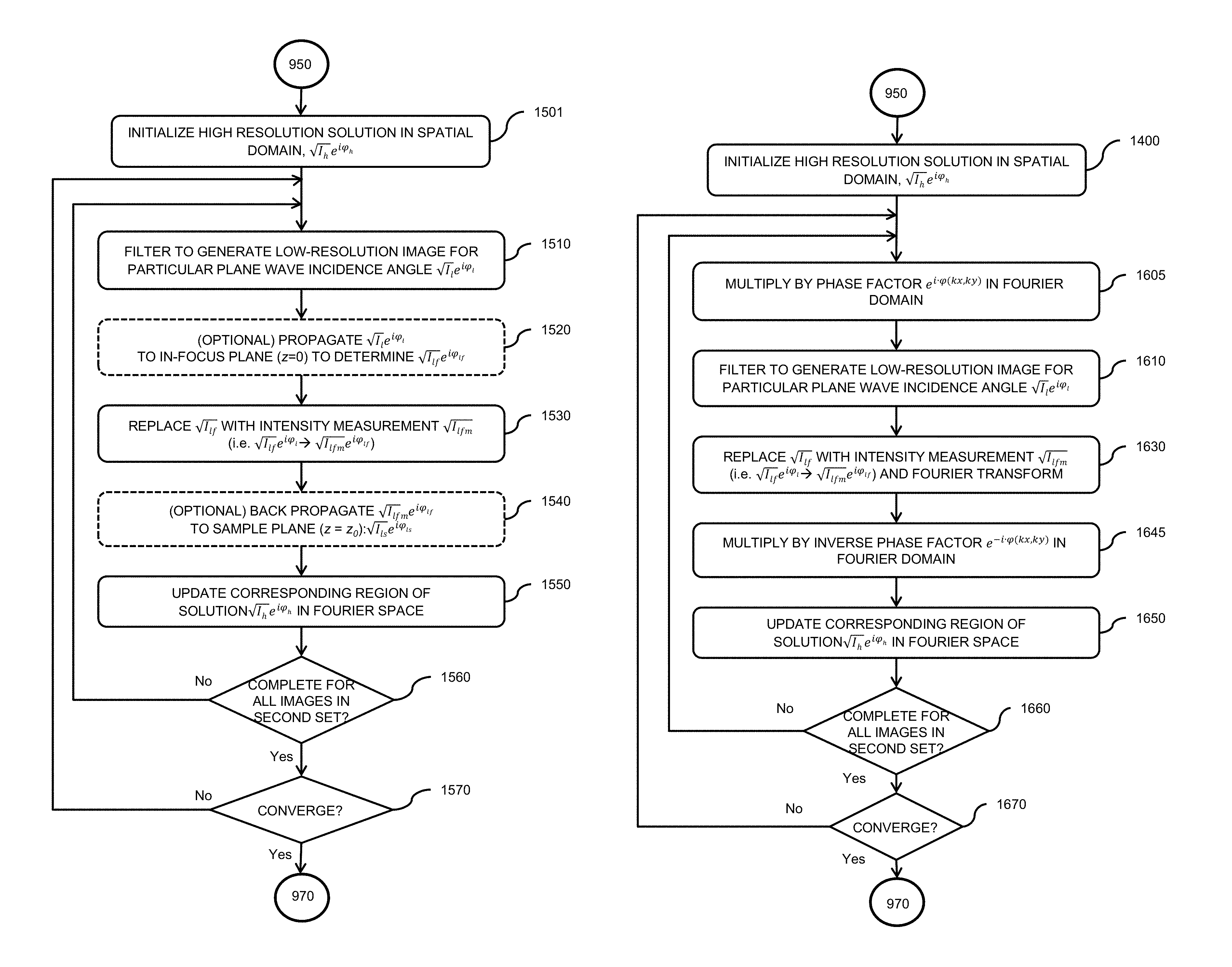
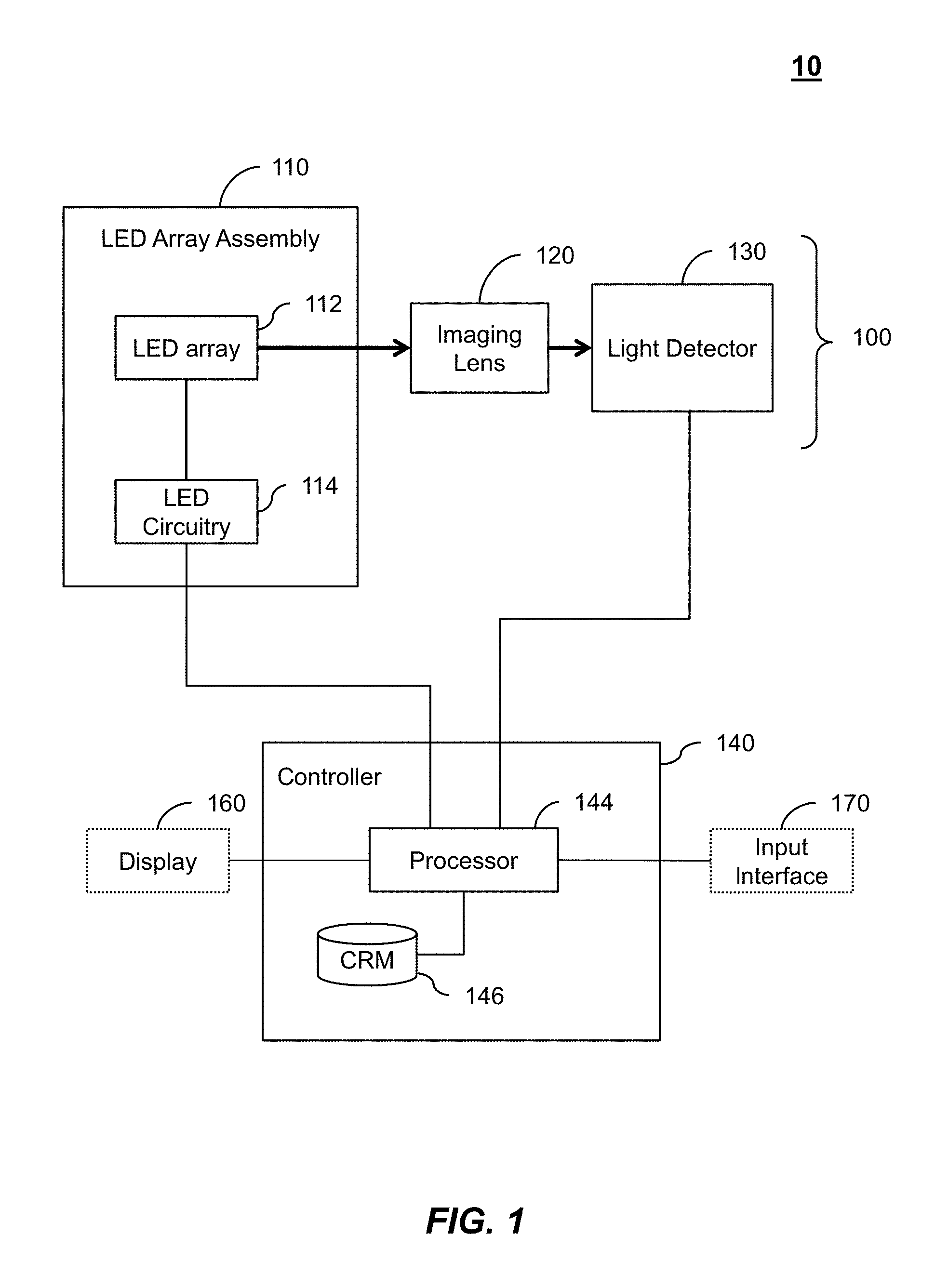
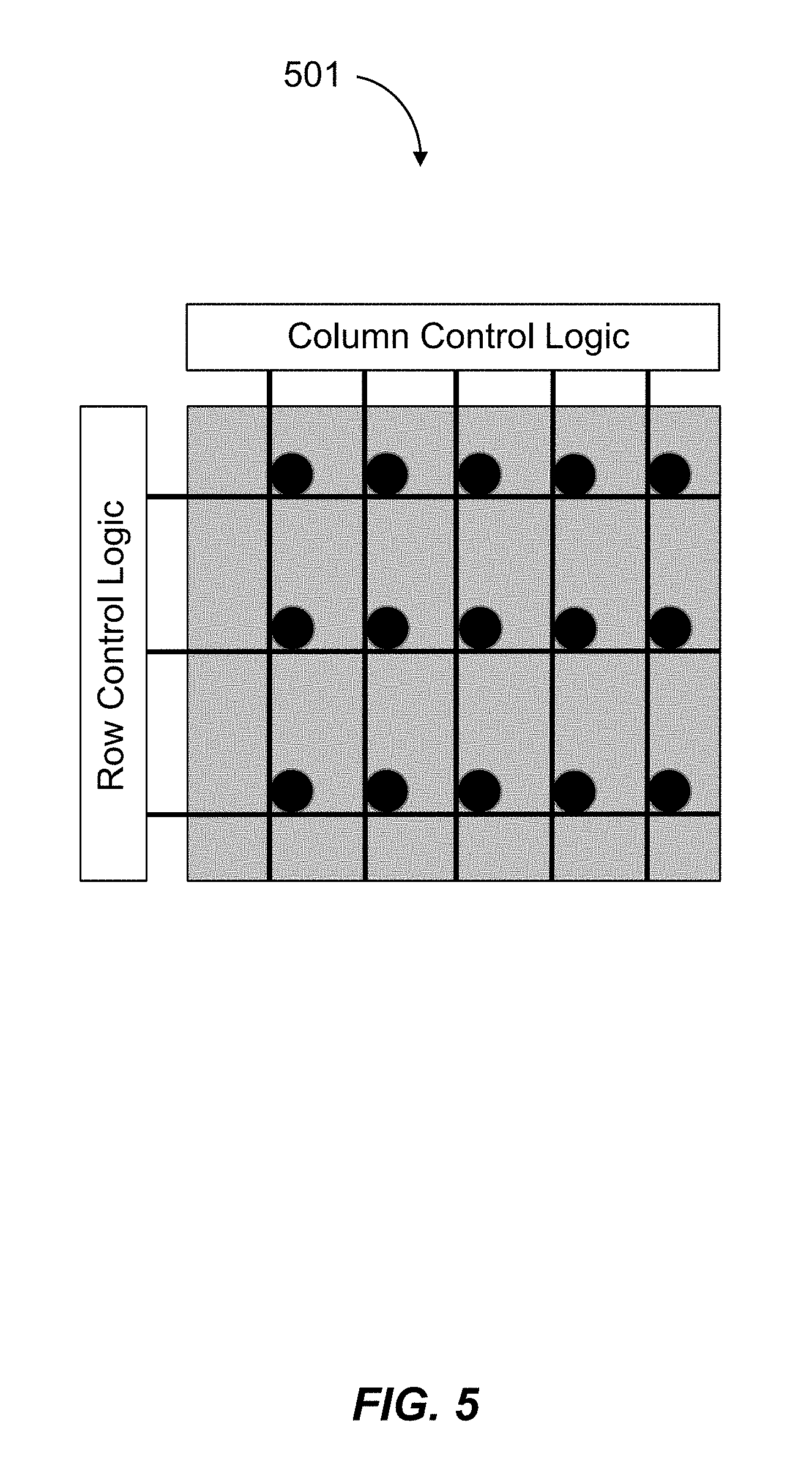
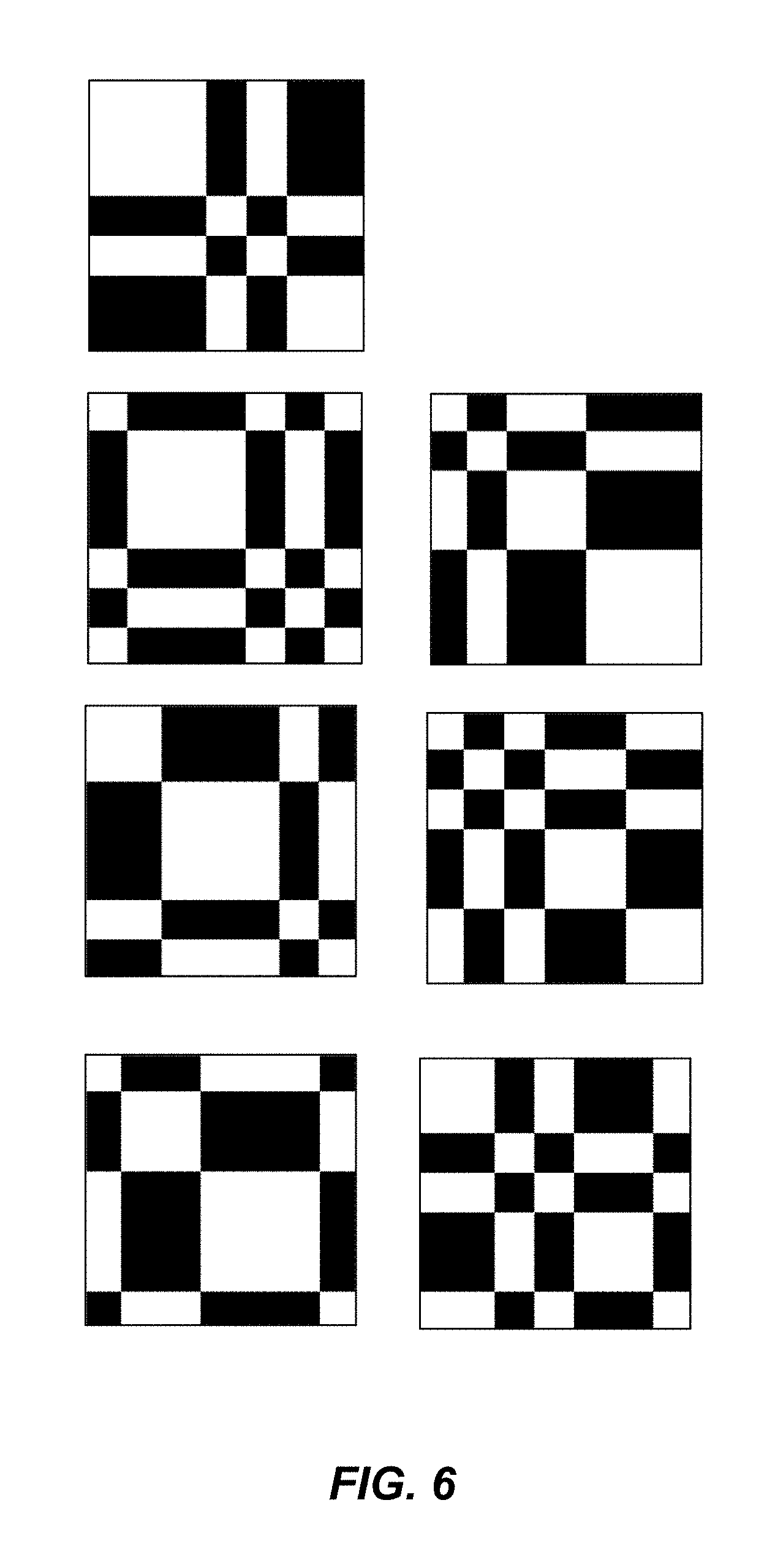
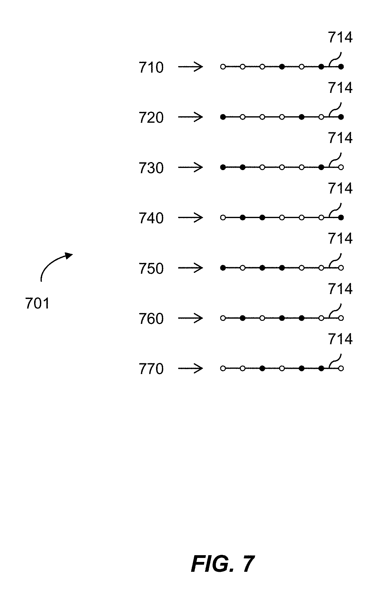
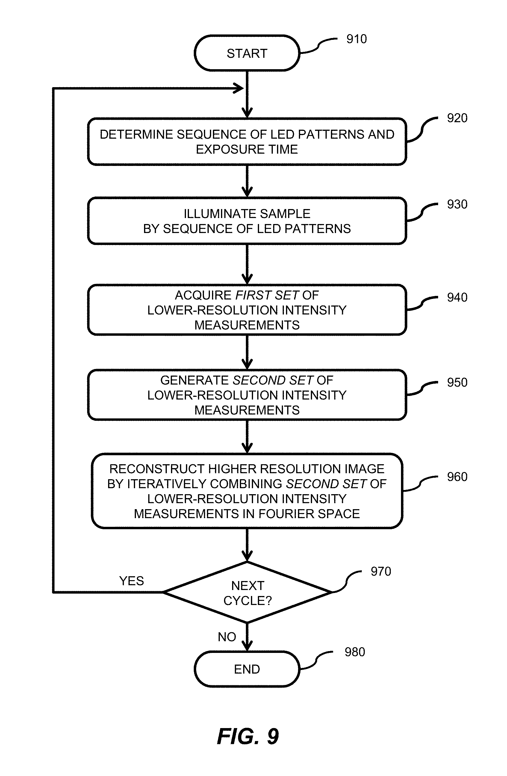
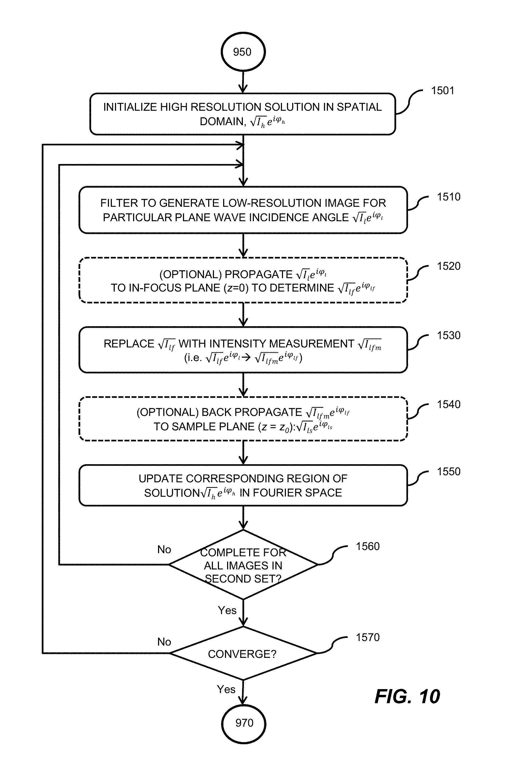
1. A multiplexed Fourier Ptychographic imaging system comprising: a light emitting diode (LED) array configured to illuminate a sequence of different LED patterns to provide multiplexed illumination, each LED pattern comprising a plurality of illuminated LEDs, the LED array located to illuminate a sample being imaged; LED circuitry in electrical communication with the LED array, wherein the LED circuitry is configured to independently control power to turn on multiple LEDs simultaneously in each LED pattern; a lens configured to collect light issuing from the illuminated sample; a light detector configured to receive light collected by the lens and to acquire a first set of lower resolution images associated with the sequence of LED patterns, wherein each lower resolution image of the first set is based on light issued from the illuminated sample and received during an exposure time; and a processor configured to execute instructions to: a) use the first set of lower resolution images based on multiplexed illumination to generate a second set of lower resolution images, wherein each image of the second set is associated with one LED in the LED array, and b) generate a higher resolution complex image of the sample using a phase-retrieval operation to recover phase data from the second set of lower resolution images by: (i) initializing a higher resolution solution in Fourier domain; (ii) low pass filtering the initial higher resolution solution to generate data in a plurality of regions of the Fourier domain; (iii) inverse Fourier transforming data in a region of the plurality of regions to generate image data, replacing amplitudes of the image data with the square root of intensity measurements from an image of the second set of lower resolution images associated with an LED corresponding to the region in the Fourier domain to produce updated image data, Fourier transforming the updated image data, and update data in the region of the Fourier domain with the Fourier-transformed updated image data; (iv) repeating operations in (iii) for each region of the plurality of the regions to determine an updated higher resolution image; and (v) iteratively determining one or more updated higher resolution solutions by repeating operations in (iv) until a comparison of data derived from a current updated higher resolution solution in the one or more updated higher resolution solutions and data derived from a previous higher resolution solution or the initial higher resolution solution is less than a predefined value, wherein the higher resolution complex image has higher resolution than the second set of lower resolution images.
2. The multiplexed Fourier Ptychographic imaging system of claim 1, wherein the processor is further configured to send control signals through the LED circuitry to the LED array to turn on multiple LEDs simultaneously in each LED pattern.
3. The multiplexed Fourier Ptychographic imaging system of claim 1, wherein the LED circuitry comprises a wire from each LED in the LED array to control logic of the processor.
4. The multiplexed Fourier Ptychographic imaging system of claim 1, wherein the processor is further configured to execute instructions for determining the sequence of LED patterns and the exposure time.
5. The multiplexed Fourier Ptychographic imaging system of claim 4, wherein the LED patterns and the exposure time are determined based on tuning input.
6. The multiplexed Fourier Ptychographic imaging system of claim 4, wherein the processor is configured to determine the LED patterns and the exposure time based on one or both of a processing time of the Fourier Ptychographic imaging system and a signal-to-noise ratio (SNR) of images acquired during operation.
7. The multiplexed Fourier Ptychographic imaging system of claim 4, wherein the processor is further configured to execute instructions for determining the sequence of LED patterns and the exposure time based on one or both of a maximum processing time and a minimum SNR.
8. The multiplexed Fourier Ptychographic imaging system of claim 1, wherein each LED pattern in the sequence is a Hadamard pattern.
9. The multiplexed Fourier Ptychographic imaging system of claim 8, wherein each LED pattern has a number of LEDs equal to more than half the total number of LEDs in the LED array.
10. An LED assembly in a multiplexed Fourier Ptychographic imaging system, the LED array assembly comprising: an LED array configured to sequentially illuminate different LED patterns of a sequence of LED patterns to provide multiplexed illumination, the LED array located to illuminate a sample being imaged; and LED circuitry in electrical communication with the LED array, wherein the LED circuitry is configured to independently control power to turn on multiple LEDs simultaneously in each LED pattern, and instructions that determine the sequence of LED patterns and the exposure time based on tuning input including a processing time and a signal-to-noise ratio (SNR), wherein the processing time is for using a first set of lower resolution images captured during the multiplexed illumination to generate a second set of lower resolution images, each image of the second set associated with one LED in the LED array, and for generating a higher resolution complex image of the sample using a phase-retrieval operation to recover phase data from the second set of lower resolution images by: (i) initializing a higher resolution solution in Fourier domain; (ii) low pass filtering the initial higher resolution solution to generate data in a plurality of regions of the Fourier domain; (iii) inverse Fourier transforming data in a region of the plurality of regions to generate image data, replacing amplitudes of the image data with the square root of intensity measurements from an image of the second set of lower resolution images associated with an LED corresponding to the region in the Fourier domain to produce updated image data, Fourier transforming the updated image data, and update data in the region of the Fourier domain with the Fourier-transformed updated image data; and (iv) repeating operations in (iii) for each region of the plurality of the regions to determine an updated higher resolution image; and (v) iteratively determining one or more updated higher resolution solutions by repeating operations in (iv) until a comparison of data derived from a current updated higher resolution solution in the one or more updated higher resolution solutions and data derived from a previous higher resolution solution or the initial higher resolution solution is less than a predefined value, wherein the higher resolution complex image has higher resolution than the second set of lower resolution images.
11. The LED array assembly of claim 10, wherein the LED array receives control signals to illuminate the sequence of LED patterns from a controller through the LED circuity.
12. The LED array assembly of claim 11, wherein the LED circuitry comprises a wire from each LED in the LED array to control logic of a processor.
13. The LED array assembly of claim 11, wherein the control signals for illuminating the sequence of LED patterns is based on tuning input of one or both of a maximum processing time and a minimum SNR.
14. A multiplexing Fourier Ptychographic imaging method comprising: multiplexed illuminating of a sample by a sequence of light emitting diode (LED) patterns using an LED array; collecting light issuing from the sample using a lens; acquiring a first set of low resolution images of the sample using a light detector receiving light collected by the lens, each low resolution image of the first set captured during an exposure time while one of the LED patterns is illuminated, wherein each low resolution image of the first set is based on light issuing from the sample; generating a second set of low resolution images of the sample using the first set, wherein each low resolution image of the second set is associated with a single LED in the LED array patterns; and reconstructing a high resolution complex image of the sample using a phase-retrieval operation to recover phase data from the second set of low resolution images by: (i) initializing a higher resolution solution in Fourier domain; (ii) low pass filtering the initial higher resolution solution to generate data in a plurality of regions; (iii) inverse Fourier transforming data in a region of the plurality of regions to generate image data, replacing amplitudes of the image data with the square root of intensity measurements from an image of the second set of lower resolution images associated with an LED corresponding to the region in the Fourier domain to produce updated image data, Fourier transforming the updated image data, and replacing data in the region with the Fourier-transformed updated image data; (iv) repeating operations in (iii) for each region of the plurality of the regions to determine an updated higher resolution image; and (v) iteratively determining one or more updated higher resolution solutions by by repeating operations in (iv) until a comparison of data derived from a current updated higher resolution solution in the one or more updated higher resolution solutions and data derived from a previous higher resolution solution or the initial higher resolution solution is less than a predefined value, wherein the higher resolution complex image has higher resolution than the second set of lower resolution images.
15. The multiplexing Fourier Ptychographic imaging method of claim 14, further comprising selecting the LED patterns and the exposure time based on one or both of a processing time and a signal-to-noise ratio.
16. The multiplexing Fourier Ptychographic imaging method of claim 15, further comprising receiving tuning input that includes the processing time or is related to the processing time.
17. The multiplexing Fourier Ptychographic imaging method of claim 14, wherein multiplexed illuminating of the sample with LED patterns comprises receiving control signals at the LED array to independently turn on each LED of each of the sequence of LED patterns.
18. The multiplexing Fourier Ptychographic imaging method of claim 15, wherein selecting the LED patterns and the exposure time comprises selecting instructions for sending control signals to the LED array for illuminating the sequence of LED patterns.
Description
BACKGROUND
Certain embodiments described herein are generally related to digital imaging, and more specifically, to Multiplexed Fourier Ptychographic imaging systems and their components, and Multiplexed Fourier Ptychographic imaging methods.
Ptychography imaging involves collecting lower resolution intensity images and reconstructing them into a higher resolution image. Over the past two decades, ptychographic imaging has been used in a variety of regimes to produce high-resolution, wide field-of-view images of microscopic and nanoscopic phenomena. Whether in the X-ray regime at third-generation synchrotron sources, in the electron microscope for atomic scale phenomena, or in the in the optical regime for biological samples, ptychography has shown an unparalleled ability to acquire hundreds of megapixels of sample information near the diffraction limit. Typically, the underlying operation of ptychography is to sample a series of diffraction patterns from a sample as it is scanned through a focused beam. These intensity-only measurements are then reconstructed into a complex (i.e. amplitude and phase), high-resolution image with more pixels of sample information than any single recorded diffraction pattern.
Recently, a Fourier ptychographic imaging technique was introduced that constructs a high-resolution sample complex, high-resolution image from a series of low-resolution intensity measurements captured while the sample of interest is sequentially illuminated from different incidence angles. In one particular implementation, a Fourier ptychographic microscopy (FPM) system uses an array of light emitting diodes (LEDs) located beneath, a thin, semi-transparent sample of interest. Each LED approximates a point illumination source. During image acquisition, the FPM system sequentially turns on individual LEDs to provide illumination incident to the sample from different angles. The light from each LED passes through the thin sample and to an imaging lens (e.g., a conventional microscope objective). The light detector receives diffraction patterns from the imaging lens and captures intensity measurements to form a unique lower resolution image for each incidence angle. The set of lower resolution images acquired during sequential illumination by different incidence angles can be reconstructed into a high-resolution complex measurement through a phase-retrieval operation. An example of this standard Fourier ptychographic imaging technique and an FPM system that implements this technique can be found in Zheng, Guoan, Horstmeyer, Roarke, and Yang, Changhuei, "Wide-field, high-resolution Fourier ptychographic microscopy," Nature Photonics vol. 7, pp. 739-745 (2013) and in U.S. patent application Ser. No. 14/065,280, titled "Fourier Ptychographic Imaging Systems, Devices, and Methods" and filed on Oct. 28, 2013; which are hereby incorporated by reference in their entirety and for all purposes.
SUMMARY
Certain embodiments pertain to digital imaging, and more specifically, to Multiplexed Fourier Ptychographic imaging systems and their components, and Multiplexed Fourier Ptychographic imaging methods.
Certain embodiments pertain to a multiplexed Fourier Ptychographic imaging system. The system comprises an LED array configured to illuminate a sequence of LED patterns, the LED array located to illuminate a sample being imaged. The system further comprises LED circuitry in electrical communication with the LED array, wherein the LED circuitry is configured to independently control power to turn on multiple LEDs simultaneously in each LED pattern. The system further comprises a lens configured to collect light issuing from the illuminated sample. The system further comprises a light detector configured to receive light from the lens to acquire a first set of lower resolution images associated with the sequence of LED patterns, wherein each lower resolution image is based on light received during an exposure time. The system further comprises a processor configured to use the first set of lower resolution images to generate a second set of lower resolution images associated with each LED in the LED array and to iteratively update overlapping regions in the Fourier domain with the second set of lower resolution images to generate a higher resolution image.
Certain embodiments pertain to an LED array assembly in a multiplexed Fourier Ptychographic imaging system. The LED array assembly generally comprises an LED array and LED circuitry in electrical communication with the LED array. The LED array is configured to illuminate a sequence of LED patterns, the LED array located to illuminate a sample being imaged. The LED circuitry is configured to independently control power to turn on multiple LEDs simultaneously in each LED pattern.
Certain embodiments pertain to a multiplexing Fourier Ptychographic imaging method. The method comprises multiplexed illuminating of a sample by a sequence of LED patterns. The method collects light issuing from the illuminated sample using a lens. The method acquires a first set of low resolution images of the sample using a light detector receiving light from the lens. Each low resolution image captured during an exposure time while one of the LED patterns is illuminated. The method generates a second set of low resolution images of the sample using the first set. Each low resolution image of the second set of images is associated with a single LED in the LED patterns. The method reconstructs a higher resolution image of the sample by iteratively updating overlapping regions in Fourier space with the second set of low resolution images.
These and other features are described in more detail below with reference to the associated drawings.
BRIEF DESCRIPTION OF THE DRAWINGS
FIG. 1 is a block diagram of components of a Multiplexed Fourier ptychographic imaging system, according to embodiments.
FIG. 2 is a schematic drawing of a side view of an image collection assembly, according to an embodiment.
FIG. 3 is a schematic drawing of a perspective view of an image collection assembly, according to an embodiment.
FIG. 4 is a schematic drawing of an LED array assembly with LED circuitry that can provide constant power simultaneously to any and all LEDs within the LED array, according to an embodiment.
FIG. 5 is a schematic drawing of a LED array assembly, according to an embodiment.
FIG. 6 is a drawing of seven 2D LED patterns, according to an embodiment.
FIG. 7 is a schematic illustration of a sequence of LED patterns in a one-dimensional LED array, according to an embodiment.
FIG. 8 is a schematic illustration of a one-dimensional LED array with seven LEDs where only one LED is turned on during each image acquisition, according to an embodiment.
FIG. 9 is a flowchart of a Multiplexed Fourier ptychographic imaging method, according to embodiments.
FIG. 10 is a flowchart of a reconstruction process, according to an embodiment.
FIG. 11 is a flowchart of a reconstruction process, according to an embodiment.
FIG. 12 is a block diagram of one or more subsystems that may be present in certain Multiplexed Fourier ptychographic imaging systems, according to embodiments.
DETAILED DESCRIPTION
Embodiments of the present invention will be described below with reference to the accompanying drawings. The features illustrated in the drawings may not be to scale.
Certain embodiments pertain to multiplexed Fourier Ptychographic imaging systems, system components, and methods. In certain aspects, a multiplexed Fourier Ptychographic imaging system comprises an LED array assembly with circuitry connected to an LED array for independently controlling power to turn on multiple LEDs simultaneously in each pattern of a sequence of LED patterns for multiplexed illumination of a sample. The system further comprises a processor in communication with the LED circuitry and in communication with a light detector. The system determines the sequence of LED patterns and exposure time to use during each cycle and sends control signals to control the turning on of the individual LEDs to illuminate the LED patterns during image acquisition. The system further comprises an imaging lens (e.g. objective lens) located to receive light issuing from the illuminated sample. The system comprises a light detector positioned to receive diffraction patterns transferred from the imaging lens based on light issuing from the illuminated sample. The light detector receives photons and takes intensity measurements for an exposure time during illumination by each LED pattern to acquire a single lower resolution image. The processor sends control signals to the light detector to control image acquisition by the light detector based on the determined exposure time. During each cycle, the light detector acquires a first set of lower resolution images while the sample is illuminated by the sequence of LED patterns. Using the first set of lower resolution images, the system generates a second set of lower resolution images and this second set of lower resolution images is used to generate a higher resolution image.
During each cycle, the system determines a sequence of LED patterns and an exposure time to use during the cycle. Multiple LEDs of each pattern are turned on simultaneously in the LED array to illuminate the sample during each image acquisition. The imaging lens receives light issuing from the sample and the light detector received light transferred from the imaging lens. To acquire each image, the light detector receives photons and samples intensity measurements for an exposure time while a single LED pattern is illuminated. During each process cycle, the light detector acquires a first set of lower resolution images during illumination by a sequence of LED patterns. In some cases, the processor determines the LED patterns and exposure time based on a maximum processing time and/or minimum signal-to-noise ratio (SNR). For example, an operator may provide tuning input with one or more of a maximum processing time and a minimum SNR. In one case, the processor can determine an exposure time that will keep the total processing time during the cycle below the maximum processing time and/or LED patterns that will cause the images acquired to have an SNR above the minimum SNR. After capturing the first set of lower resolution images, a weighted sum operation of the first image data set is performed to re-create a second image data set that would have been captured had a single LED been turned on at each image acquisition time. After this weighted sum operation, a high resolution amplitude and phase map of the image sample can be reconstructed based on the second data set. Details of reconstruction processes that can be used are found in Section III, in Zheng, Guoan, Horstmeyer, Roarke, and Yang, Changhuei, "Wide-field, high-resolution Fourier ptychographic microscopy," Nature Photonics, vol. 7, pp. 739-745 (2013), and in U.S. patent application Ser. No. 14/065,280, titled "Fourier Ptychographic Imaging Systems, Devices, and Methods" and filed on Oct. 28, 2013.
Data capture for standard Fourier ptychography imaging techniques is generally performed by illuminating one LED at a time from within a large array of N LEDs, and acquiring a digital image for each illuminated LED based on a specific incidence angle. Where N may be several hundred LEDs, the data capture process can be time consuming. For example, a standard Fourier ptychography imaging system that uses 225 LEDs to take 225 images with a 1 second exposure time would have total image acquisition time of 225 seconds.
Instead of turning on a single LED for each image acquired, a multiplexed Fourier Ptychographic imaging system of embodiments uses multiplexed illumination. The system is designed with an LED array assembly that can turn on any LED in the LED array to turn on unique patterns of a sequence of LED patterns. In one example, the LED patterns may have up to 1/2 or 3/4 of the total number of LEDs for each image. After capturing N different images, each under illumination from a unique pattern, it is possible to linearly combine the resulting images to generate a second data set that would have captured had individual LEDs been illuminated in the array. Since, however, each image is illuminated with light that much brighter than when using just a single LED, a much shorter exposure time per image can be used resulting in a much faster data acquisition process.
In certain aspects, multiplexed Fourier Ptychographic imaging systems and methods are configured to improve the rate at which high resolution images are generated since the exposure time can be reduced significantly for the same noise. As discussed above, certain standard Fourier Ptychographic imaging techniques are based on turning on a single LED at each acquisition time to illuminate the sample from a single incidence angle. The multiplexed Fourier Ptychographic imaging technique turns on multiple LEDs simultaneously in a unique pattern during each image acquisition. In order to provide patterned illumination, the multiplexed Fourier Ptychographic imaging system includes an LED array assembly with circuitry and processor designed for independent control of each LED in the array so that any of the LEDs can be turned on simultaneously to illuminate unique patterns. Since each low-resolution image is based on significantly more photons received at the light detector, the noise is reduced for each image acquired. Since this is the case, the multiplexed Fourier Ptychographic imaging system can reduce the exposure time significantly while maintaining the same noise. Reducing the exposure time at each image acquisition reduces the overall processing time. The amount of noise is based on the number of LEDs illuminated in each pattern. In some aspects, the system is tunable to adjust the processing time by selecting a particular exposure time and/or to adjust the SNR by selecting a particular sequence of LED patterns. For example, an operator of the system can provide tuning input to keep the processing time below a processing time provided by the operator and also keep the noise below a particular level associated with an SNR. For example, a multiplexed Fourier ptychography imaging system that uses 225 LEDs to take 225 images can simultaneously turn on 113 of the 225 LEDs for each unique pattern during image acquisition. While maintaining the same amount of noise, exposure time can be reduced by a factor of sqrt (225)/2=7.5. That is, if the original exposure time is 1 second per acquisition using 1 LED illuminated at each acquisition, the new exposure time used by the multiplexed Fourier Ptychographic imaging system can be reduced to 1/7.5=0.13 seconds while maintaining the same noise. In this case, the total image acquisition time can be reduced from 225 to 225*0.13 seconds=30 seconds.
I. Multiplexed Fourier Ptychographic Imaging Systems
FIG. 1 is a block diagram of components of a Multiplexed Fourier ptychographic imaging system 10, according to embodiments. The system 10 includes an image collection assembly 100 comprising an LED array assembly 110, an imaging lens 120, and a light detector 130 for taking intensity measurements. The LED array assembly 110 comprises an LED array 112 configured to illuminate a sample (not shown) being imaged and circuitry 114. The system 10 also includes a controller 140 having a processor 144 and a CRM (i.e. computer readable medium) 146, an optional (depicted by dotted line) display 160, and an optional (depicted by dotted line) input interface 170. The LED circuitry 114 is in electrical communication with the LED array 112 and the processor 144 of the controller 140. The LED circuitry 114 is configured to provide power to independently turn on each LED in the LED array 112. The processor 144 determines the sequence of LED patterns and sends control signals through the circuitry 114 to the LED array 112 illuminate the sequence of LED patterns. The arrow between the LED array 112 and imaging lens 120 depicts that the imaging lens 120 is located to receive light issuing from the sample illuminated by coherent light from the LED array 112. The arrow between the imaging lens 120 and the light detector 130 depicts that the light detector 130 is configured to receive light issuing from the sample as transferred from the imaging lens 120. The light detector 130 sequentially captures a first set of lower resolution images of the sample illuminated by the sequence LED patterns where each low-resolution image is based on intensity measurements taken over an exposure time. As used herein, an exposure time generally refers to a duration of time during which a light detector collects photons, integrates the total energy from the collected photons into an electric potential, and uses this potential as a measure of intensity at each discrete light detecting element (e.g., pixel) to form the image data that comprises a single lower resolution image.
The Multiplexed Fourier ptychographic imaging system 10 includes a processor 144 and a CRM 146, an optional display 160, and an input interface 170. In one example, one or more of these components may be part of a single computing device such as, for example, a smartphone, laptop, desktop, tablet, etc. The optional display 160, optional input interface 170, and CRM 146 are all in communication with the processor 144. The processor 144 of controller 140 determines the sequence of LED patterns and exposure time to use during image acquisition and also generates a high-resolution image from the intensity data of the first set of lower resolution images acquired by the light detector 130. The processor 144 is also in communication with the light detector 130 and the LED circuitry 114 to send a control signals to synchronize the illumination of the LED patterns with the exposure times for acquiring the first set of lower resolution images with the illumination times of the sequence of LED patterns. That is, the processor 144 sends control signals to the LED array 112 through the LED circuitry 114 with instructions to illuminate the sequence of LED patterns. The processor 144 sends control signals to the light detector 130 to receive photons for exposure times while the LED array is illuminated by the sequence LED patterns.
FIGS. 2 and 3 are schematic drawings of components of image collections assemblies that may be used in a Multiplexed Fourier ptychographic imaging system such as the system shown in FIG. 1. FIG. 2 is a schematic drawing of a side view of an image collection assembly 200, according to an embodiment. The image collection assembly 200 comprises an LED array assembly 210 with an LED array 212 located to illuminate a sample 20, an imaging lens 220, and a light detector 230 for measuring intensity from photons received at its active sensing surface. In this example, the image collection assembly 200 is arranged in trans-illumination mode directing illumination through the sample being imaged while the imaging lens 220 receives light transmitted through the sample 21. In this illustrated example, the LED array 212 is one-dimensional LED array with seven LEDs. In this illustration, an LED pattern is shown with four illuminated LEDs 214 and three non-illuminated LEDs 215. During image acquisition, the LEDs receive control instructions though circuitry (not shown) from a controller (not shown) and execute the control instructions to illuminate a sequence of LED patterns. The system 200 further comprises an imaging lens 220 that receives and accepts light based on its NA issuing from the illuminated sample 20. In certain cases, the imaging lens 220 is located at a Fourier plane of the sample plane. The light detector 230 receives illumination transferred from the imaging lens 220 and measures intensity data for an exposure time to capture each low-resolution image. During an image acquisition operation, the light detector 230 measures intensity data to acquire a first set of lower resolution images while the sample 20 is illuminated by a sequence of illuminated LED patterns.
FIG. 3 is a schematic drawing of a perspective view of an image collection assembly 300, according to an embodiment. The image collection assembly 200 comprises an LED array assembly 310 with an LED array 312 configured to illuminate a sample 22, an imaging lens 320 (e.g. objective lens), and a light detector 330. The LED array 312 is a two-dimensional LED array (20.times.20) with 400 LEDs. An arrow is depicted showing the angle of illumination of a particular LED in the array 312. During operation, the LEDs receive control instructions though circuitry (not shown) from a controller (not shown) and execute the control instructions to illuminate a sequence of LED patterns. The imaging lens 320 receives and accepts light based on its NA issuing from the illuminated sample 21. In certain cases, the imaging lens 320 is located at a Fourier plane of the sample plane. The light detector 330 receives illumination transferred from the imaging lens 320 and measures intensity data for an exposure time to capture each low-resolution image. During an image acquisition operation, the light detector 330 measures intensity data for a sequence of lower resolution images while the sample 21 is illuminated by a sequence of illuminated LED patterns.
According to certain aspects, the components of the image collection assembly may be arranged to operate in either trans-illumination mode (i.e. imaging lens collecting light transmitted through the sample) or in reflective mode (i.e. light reflected from the sample is collected at the imaging lens). In FIG. 2, for example, the components of the image collection assembly 200 are arranged to operate in trans-illumination mode where the LED array 212 and imaging lens 220 are located to direct illumination through the sample 20 while the imaging lens 220 receives light transmitted through the sample 20. To operate in reflection mode, the LED array and imaging lens would be located to direct illumination toward the sample and the imaging lens located to receive light reflected from the sample.
During a typical cycle of a Multiplexed Fourier ptychographic imaging system, a processor determines a sequence of LED patterns to illuminate during image acquisition by the light detector. The processor also determines an exposure time for the light detector to receive photons and measure intensity values for each image acquisition. The processor sends control signals to both the light detector and to the LED array with control data to synchronize the illumination of each LED pattern with image acquisition. The processor may send control data comprising, for example, one or more of a start time for the image acquisition operation, the determined exposure time for each image acquisition and corresponding duration of illumination of each LED pattern, and the number of images acquired, and data for illuminating the determined sequence of LED patterns. During image acquisition, the processor independently controls through the circuitry each LED in the LED array to turn on LEDs in the sequence of LED patterns. The imaging lens receives light issuing from the sample and transfers light to the light detector. The light detector receives photons and samples intensity measurements during the determined exposure time while each LED pattern is illuminated. During the image acquisition process of each cycle, the light detector sequentially captures a first set of lower resolution images of the sample while the sample is being illuminated by the determined sequence of LED patterns. The processor performs a weighted sum operation on the first image data set to re-create a second image data set that would have been captured had a single LED been turned on at each image acquisition time. The processor reconstructs a high resolution amplitude and phase map of the image sample using the second image data set.
Generally, a sample can comprise one or more objects of interest. For example, a sample may be a biological specimen with one or more cells or cell organelles. As another example, the sample may be a semiconductor wafer. In some cases, the one or more objects in the sample are thin and/or translucent.
In certain aspects, the Multiplexed Fourier ptychographic imaging system comprises an LED array assembly comprising an LED array and LED circuitry. The LED circuitry provides electrical communication between each LED in the LED array and a processor, for example, of a controller. That is, the processor is electrically connected through the LED circuitry to the LED array to be able to send control signal(s) to turn on LEDs of each LED pattern in the sequence of LED patterns.
The LED array assembly comprises an LED array with n.times.m dimensions for providing illumination. The LED array can be a one-dimensional array (1.times.m where n=1) or a two-dimensional array of discrete LEDs. Some examples of dimensions of the LED array are 6.times.6, 7.times.7, 8.times.8, 9.times.9, 10.times.10, 32.times.32, 50.times.50, 20.times.20, 30.times.30, 60.times.60, 100.times.100, 50.times.10, 20.times.60, 1.times.10, 1.times.7, 1.times.20, 1.times.30, etc. Other dimensions may be used. Each LED in the LED array can be approximated as a point light emitter. Although, the LED array is described in many cases as a single LED at each location of the array, each location may have multiple LEDs in some cases. For example, each location in the array may have blue, green, and red LEDs. In some cases, the LEDs provide visible light wavelengths. In other cases, the LEDs provide ultraviolet light wavelengths. In other cases, the LEDs provide infrared light wavelengths.
In certain aspects, a Multiplexed Fourier ptychographic imaging system comprises an LED array assembly with LED circuitry that can provide power (e.g., voltage) to any combination of LEDs in the LED array simultaneously, without needing to vary the power delivered to each LED over time while it is in the "on" state. In other words, the LED circuitry can simultaneously provide a constant power (i.e., voltage) to any and all LEDs within the array that must be in the "on" state. That is, the LED circuitry is designed to allow for independent control of turning on/off any combination of LEDs in the array simultaneously. In one example, the LED circuitry includes an electrical connection (e.g. wire) between each LED and the processor.
FIG. 4 is a schematic drawing of an LED array assembly 410 with LED circuitry 412 that can simultaneously provide a constant power (i.e., voltage) to any and all LEDs within the LED array that must be in the "on" state, according to an embodiment. The LED array assembly 410 comprises a 3.times.5 LED array 412 and individually addressed LED circuitry 414. The arrow indicating LED circuitry 414 points to a single wire in the LED circuitry 414 but it would be understood that there are 15 wires in this illustrated LED circuitry 414. As shown, the LED circuitry 414 includes a single wire between each LED in the array 412 and the control logic of the controller (e.g., microcontroller). Single wires provide the ability to control DC voltage/current to each LED individually. That is, the LED array 412 is an individually addressed array.
Conventional LED arrays are typically designed with electrical connections to turn on a single LED at a time where each LED is controlled by setting values to its associated row and column. Such LED arrays are often referred to as multiplexed displays. A related form of display is often referred to as a charlieplexed display. For example, in one conventional LED array, often referred to as a dot-matrix display with a dot-matrix controller, the rows are connected to LED anodes of a microcontroller and the columns are connected to LED cathodes of the microcontroller. To turn on any of the LEDs in a column, the column needs to be on a low setting (i.e., a low voltage). To turn on any of the LEDs in a row, the rows needs to be in the high setting (i.e., a high current). If the row and column are both set to high or both set to low, no voltage flows through the LED and it does not turn on. To control an individual LED, the column is set to low and the row too high. To control multiple LEDs in a row, the row is set to high then the columns are set to low or high as appropriate to turn on respective LEDs over time. This conventional LED array does not have the ability to turn on an arbitrary group of LEDs simultaneously, since they do not have independent control of each LED. That is, the control of an LED is dependent on the row and column setting and not an individual LED. For example, this conventional LED array would not be capable of turning on LEDs along a diagonal of the array, since this will require all of the rows to be set to a low voltage and all of the columns to be set to a high voltage in our example, which will cause all of the LEDs in the array to turn on, instead of just the LEDs along the diagonal, as desired.
FIG. 5 is a schematic drawing of an LED array assembly 501 with a 3.times.5 row/column addressed LED array. In this example, the circuitry is designed to control the DC voltage/current only along the entire row/column.
Since conventional LED arrays (e.g., dot-matrix displays or charlieplexed displays) cannot turn on any group of LEDs in the LED array, they often turn on each LED in the desired pattern individually and very quickly (i.e., within less than 30 milliseconds, which is the approximate integration time of the human eye). While this is helpful for displaying content in the LED display to a user, it is not helpful for delivering a constant amount of optical power over time from each LED to evenly illuminate, e.g., a specimen for multiplexed illumination.
In certain aspects, a Multiplexed Fourier ptychographic imaging system comprises an imaging lens for collecting light issuing from the sample. Typically, the imaging lens is located at a Fourier plane of the sample plane. The imaging lens may be, for example, an objective lens that only accepts light within a range of incidence angles based on its numerical aperture (NA). In one case, the imaging lens is an objective lens with an NA of about 0.08. In another case, the imaging lens is an objective lens with an NA in the range between about 0.01 and about 0.1.
In certain aspects, the Multiplexed Fourier ptychographic imaging system comprises a light detector having a two-dimensional grid of equally spaced discrete detecting elements (e.g., pixels). During each exposure time, the light detector collects photons, integrates the total energy from the collected photons into an electric potential, and uses this potential as a measure of intensity at each discrete light detecting element (e.g., pixel) to form the image data that comprises a single lower resolution image. The light detector generates a signal(s) with lower resolution images of image data of the intensity distribution measured by the grid of discrete light detecting elements during the cycle. If visible light radiation is being used to illuminate the sample, the light detector may be in the form of a charge coupled device (CCD), a CMOS imaging sensor, an avalanche photo-diode (APD) array, a photo-diode (PD) array, a photomultiplier tube (PMT) array, or like device. If using THz radiation is used, the light detector may be, for example, an imaging bolometer. If X-ray radiation is used, the light detector may be, for example, an x-ray sensitive CCD. These examples of light detectors and others are commercially available. In some aspects, the light detector may be a color detector e.g., an RGB detector. In other aspects, the light detector may be a monochromatic detector.
In certain aspects, a Multiplexed Fourier ptychographic imaging system comprises one or more processor (e.g., microprocessors) that receives instructions stored on a CRM and executes the instructions to perform one or more functions of the system. For example, the processor may execute instructions stored on the CRM to perform one or more of: 1) interpreting image data, 2) reconstructing a higher resolution image, 3) generating a second set of lower resolution image data from a first set of lower resolution image data, 4) providing display data for displaying one or more images or other output on the display, and 5) determining a sequence of LED patterns, an exposure time, control instructions for turning on LEDs in the form of LED patterns in the LED array, and/or other operations performed during one or more operations of the Multiplexed Fourier ptychographic imaging method described in Section II. The processor may be connected directly or indirectly through other devices to one or more power supplies. The one or more power supplies may be internal and/or external to the system.
In certain aspects, a Multiplexed Fourier ptychographic imaging system comprises a processor that send control signals to the LED array and/or the light detector. In some cases, these control signals synchronize the illumination of the sequence of LED patterns with the exposure times for acquiring the first set of lower resolution images. For example, the processor may send control signals to the LED array through the LED circuitry with instructions to illuminate the sequence of LED patterns and control signals to the light detector to receive photons for exposure times while the LED array is illuminated by the sequence LED patterns. The processor may also determine the sequence of LED patterns and exposure time to use during image acquisition and/or generate a high-resolution image from the first set of lower resolution images acquired by the light detector.
In certain cases, a processor can send control signals through LED circuitry to the LED array to illuminate a sequence of LED patterns. In these cases, the controller can independently control any combination of LEDs in the LED array to turn on the LEDs of each LED pattern of the sequence. The processor can also generate a high resolution image from the first of lower resolution images collected during illumination by the sequence of LED patterns. The controller may also provide display data to a display and/or may process signals with input from an input interface.
In certain aspects, a Multiplexed Fourier ptychographic imaging system comprises a CRM (e.g., memory) is in communication with one or more processors to receive data and sending data stored on the CRM. In addition to storing instructions for performing certain functions of the system, the CRM can also store lower resolution image data (first set and/or second set), higher resolution image data, input from an operator or other entity, and other data used by the system. For example, the CRM may store different sequences of LED patterns and exposure times that correspond to certain SNR levels and/or processing times. In other cases, the CRM may store instructions for calculating a sequence of LED patterns and/or an exposure time based on a particular processing time and/or a particular SNR. Alternatively, for example in the case of using Hadamard multiplexing, the CRM may store a look-up table. This look-up table may contain a list of possible number of images to acquire, ranging from 1 to N, where N can be as large as 1000 or more. For each value of N, the look-up table will contain a unique list of N different LED patterns (i.e., a list of which LEDs to turn on within the LED array and which should remain off, for each image to be captured). The look-up table might also contain a list of exposure times for each image to be captured.
In some aspects, a Multiplexed Fourier ptychographic imaging system comprises a display in communication with the processor to receive data for displaying images and other output on the display to, for example, an operator of the system. The display may be a color display or a black and white display. In addition, the display may be a two-dimensional display or a three-dimensional display. In one embodiment, the display may be capable of displaying multiple views.
In some aspects, a Multiplexed Fourier ptychographic imaging system comprises an input interface. The input interface refers to a device capable of receiving input from an operator of the system. For example, an input interface may be a keyboard, a touch screen, a microphone, etc.
A. Sequence of LED Patterns
In certain aspects, the multiplexed Fourier Ptychographic imaging system uses an LED array assembly to turn on multiple LEDs in the LED array in a sequence of LED patterns. During illumination by each LED pattern, the system captures a lower-resolution image. Although LED patterns are described in certain examples herein with respect to a square LED array having N LEDs (N=n.times.n), other LED arrays may be used.
By illuminating patterns of LEDs during each cycle, a Multiplexed Fourier ptychographic imaging system can speed up image acquisition significantly from conventional techniques by reducing exposure time while maintaining the same SNR within each image acquired. When using a square LED array, for example, the exposure time of each image acquisition (and the total duration of the image acquisition process) can be reduced by up to a factor of approximately sqrt(N)/2 for a fixed SNR within each image acquired, where again N is the number of LEDs in the array and sqrt( ) denotes a square root operation. From the theory of Hadamard multiplexing, the exact exposure reduction is [sqrt(N)+(1/sqrt(N)]/2, which approaches the above approximation for large N, and assumes the predominant source of noise effecting the SNR is statistically independent and additive. Put another way, if the system can use the same image exposure time as would have been used when turning on a single LED, then the SNR of each detected image will be improved by the same sqrt(N)/2 factor when multiplexing is used and when the noise is independent and additive. In some aspects, the system can take advantage of this flexibility by adjusting the exposure time and LED patterns to tune the system to a particular processing time and SNR combination. After data capture of a first set of N images using the illuminated LEDs arranged in patterns, the system performs a weighted sum of the N images to produce a second set of images that is analogous to what is captured when a single LED is on at each acquisition time.
Generally, the sequence of LED patterns comprises unique patterns. In most cases, each LED pattern comprises at least one LED turned on at a time. In one aspect, each LED pattern comprises less than or equal to 3N/4 LEDs turned on at a time. In one aspect, each LED pattern turns on up to half of the LEDs in the array during each image acquisition. In the case of a square LED array, each LED pattern turns on up to N/2 of the LEDs in the array for each image. In another aspect, each LED pattern turns on up to a quarter of the LEDs in the array for each image acquired. In the case of a square LED array, each LED pattern turns on up to N/4 of the LEDs in the array for each image. In another aspect, each LED pattern turns on more than a quarter of the LEDs in the array for each image acquired. In another aspect, each LED pattern turns on more than a quarter of the LEDs in the array for each image acquired. Typically, multiplexing requires that more than 1 LED is turned on at a time. In one example, a LED pattern has less than or equal to 3N/4 LEDs turned on at a time.
In some cases, the number of unique patterns in the sequence is determined by the number of LEDs that will be illuminated in the LED array or the number of images that will be acquired. In one example that uses a square (n.times.n) LED array, the number of unique patterns in the sequence is N (N=n.times.n). The number of unique patterns in the sequence is N and the sequence of LED patterns together form an N.times.N matrix, which can be stored and accessed appropriately as a look-up table for selecting the correct set of patterns for a given value of N. It is possible that the number of unique patterns may also be less than N, when using modified versions of the Hadamard code are used (i.e., which might take into account uneven illumination at the sample plane, LED sources that do not turn completely off, or LED sources that offer a coupled output).
In one aspect, the LED patterns in the sequence are defined by a "Hadamard" pattern also referred to as "Hadamard" code. In the case of a one-dimensional LED array (n.times.1), the number of unique patterns in the sequence is n and the sequence of LED patterns together form an n.times.n "Hadamard" matrix for a signal of length n.
FIG. 6 is a drawing of seven 2D Hadamard LED patterns out of a sequence of 49 different 2D Hadamard patterns for a 7.times.7 LED array, according to an embodiment. In case, n=7 and N=n.times.n=49. In the drawing, a white entry denotes that the associated LED is turned on, and the black entry denotes that the LED is off.
FIG. 7 is a schematic illustration of a sequence of LED patterns 701 of illumination by a one-dimensional LED array 714 that can be used to acquire seven low-resolution images in a multiplexed Fourier Ptychographic imaging system, according to an embodiment. In this particular example, the LED array 714 has seven LEDs and seven illumination patterns 710, 720, 730, 740, 750, 760, 770 are used in the sequence (N=7). Although the example is shown for simplicity based on a one-dimensional LED array, extension to patterns for a two dimensional LED array are direct. One simple way of forming the associated 2D Hadamard patterns from their 1D counterparts is to first define a Hadamard pattern for the value n, or the number of LEDs that will be used along one dimension of the LED array. Then, one should set all values in the pattern vector to -1. For example, if n=7, then for the first pattern, s=[1 1 1 0 1 0 0], and thenform s'=[1 1 1 -1 1 -1 -1]. Next, one should compute the outer product of s' with itself to form s.sub.2D'=s'*s', where * denotes an outer-product. s.sub.2D' is a 7.times.7 matrix that contains +1's and -1's in its entries. Finally, the associated 2D pattern s.sub.2D is found by setting all of the entries in s.sub.2D' that are -1 to 0, and leaving all of the entries that are +1 unchanged.
In this example, the patterns in the sequence are Hadamard patterns based on a cyclic permutation of the vector, s=[1 1 1 0 1 0 0]. The first pattern of LEDs 710 turned on will match s (first, second, third, and fifth LED turned on). The second pattern of LEDs 720 turned on will match [0 1 1 1 0 1 0] which is shifted to the right by one. The third pattern of LEDs 730 will match [0 0 1 1 1 0 1] which is shifted from the right by one and so on. The fourth pattern of LEDs 740 will match [1 0 0 1 1 1 0] which is shifted from the right by one and so on. The fifth pattern of LEDs 750 will match [0 1 0 0 1 1 1] which is shifted from the right by one and so on. The sixth pattern of LEDs 760 will match [1 0 1 0 0 1 1] which is shifted from the right by one and so on. The seventh pattern of LEDs 770 will match [1 1 0 1 0 0 1] which is shifted from the right by one and so on. In the case of displaying a pattern on an LED array in two dimensions, the above method of shifting to the right by one may be generalized to shifting a two-dimensional pattern of LEDs sequentially to the right by one column, and down by one row. Although Hadamard patterns are used, other patterns can be used based on permutations of other s vectors. The first related example takes its patterns from the Walsh matrix, which is a re-arranged version of the Hadamard S matrix. For a second example, in some applications, it might be beneficial to select the LED patterns at somewhat at random. One example of a random sequence in the above simple example is [0 1 1 0 0 1 0], [0 0 0 1 0 1 0], [1 1 1 0 1 0 1], [1 0 1 1 1 0 0], [0 1 0 0 0 0 1], [1 0 1 1 1 1 0 0], [0 1 0 1 0 0 0 0]. In other applications, it might be beneficial to select the LED patterns as a slightly modified version of the Hadamard pattern sequence, e.g. by always leaving the middle three entries at a lower total optical power than the LEDs at the remaining locations. If we let the entries within the vector s denote the amount of optical power that is emitted from each LED, then the example sequence, s.sub.1=[1 1 0.5 0 0.5 0 0] as the first pattern, s.sub.2=[0 1 0.5 0.5 0 1 0] as the second pattern, s.sub.3=[0 0 0.5 0.5 0.5 0 1], s.sub.4=[1 0 0 0.5 0.5 1 0], s.sub.5=[0 1 0 0 0.5 1 1], s.sub.6=[1 0 0.5 0 0 1 1], and s.sub.7=[1 1 0 0.5 0 0 1] might be beneficial.
After the multiplexed Fourier Ptyochographic imaging system captures a first image set of 7 lower resolution images I=[I.sub.1, I.sub.2, . . . , I.sub.7] based on the seven LED patterns shown in FIG. 7, the system can generate a second set of lower resolution images as if only one LED were turned on during each image acquisition. Here, I is a matrix that contains each detected image in one of its columns. For the case of two-dimensional images, each column of I contains the reshaped version of each two-dimensional image into a one-dimensional vector.
FIG. 8 is a schematic illustration of illuminations 801 by a one-dimensional LED array 814 with seven LEDs where only one LED is turned on during each image acquisition, according to an embodiment. In this illustrated example, the sequence of LED patterns 801 includes illumination patterns 810, 820, 830, 840, 850, 860, 870 that sequentially illuminate a single LED in the array at each acquisition time.
After the system captures the seven images based on the seven LED patterns shown in FIG. 7, the images can be linearly combined to re-create a second set of images based on the illumination patterns shown in FIG. 8, but with lower noise (for the same exposure time). To generate the second set of lower resolution images, the multiplexed Fourier Ptychographic imaging system performs a weighted sum operation on the first set. In one example, the system performs the weighted sum operation by first defining a combination vector, R, associated with the LED array dimensions. For example, for the one-dimensional LED array with seven LEDs, the combination vector R=[1 1 1 -1 1-1 -1]/4. Next, the multiplexed Fourier Ptychographic imaging system determines the matrix product L.sub.1=I R. L.sub.1 is our desired image formed from the first LED in the LED array. L.sub.j, the image formed as if just the j.sup.th LED were turned on, is given as a matrix product between the matrix I and the j.sup.th permutation of R.
The s vector of LEDs and the vector R are defined by various methods. In one example, both vectors s and R can be determined using a Hadamard code. In the LED patterns shown in FIG. 4, for example, both vectors s and R were determined using a Hadamard code for n=7. Details of the Hadamard code can be found in Schechner, Y. Y., Nayar, S. K., and Belhumeur, P. N. "Multiplexing for optimal lighting," IEEE PAMI 27, 1339-1356 (2007), which is hereby incorporated by reference for the Hadamard code. In the presence of non-additive noise, other methods may be preferred over the Hadamard code. Other sets of LEDs (i.e., random combinations) may also be a good candidate. An example of multiplexed illumination can be found in Tian, L., Li, X., Ramchandran, K., Waller, L., "Multiplexed coded illumination for Fourier ptychography with an LED microscope," Biomedical Optics Express 5(7), pp. 2376-2389 (2014), which is hereby incorporated by reference for this example. Another example may be to use random illumination sequences, in which case approximately N/2 of the LEDs within the array are turned on for each image, but these N/2 LEDs are selected uniformly at random. Finally, it may be beneficial to turn on some LEDs in the array more brightly than other LEDs within the array during the multiplexing. If we let the entries within the vector s denote the amount of optical power that is emitted from each LED, then it might be beneficial in some implementations to weight the optical power emitted from the center LEDs as less than the optical power emitted from the LEDs at the edges. In which case, the example sequence s.sub.1=[1 1 0.5 0 0.5 0 0] as the first pattern, s.sub.2=[0 1 0.5 0.5 0 1 0] as the second pattern, s.sub.3=[0 0 0.5 0.5 0.5 0 1], s.sub.4=[1 0 0 0.5 0.5 1 0], s.sub.5=[0 1 0 0 0.5 1 1], s.sub.6=[1 0 0.5 0 0 1 1], and s.sub.7=[1 1 0 0.5 0 0 1]. Here, the center 3 LEDs remain at an optical power less than the LEDs at the side.
In many aspects, each LED pattern in a sequence of LED patterns includes a number of LEDs equal to at least half the total number of LEDs in the LED array. In one example, the number of LEDs in an LED pattern is half the total number of LEDs in the LED array. In another example the number of LEDs in an LED pattern is more than half the total number of LEDs in the LED array. In another example, the number of LEDs in an LED pattern is more than 55% of the total number of LEDs in the LED array. In another example, the number of LEDs in an LED pattern is more than 60% of the total number of LEDs in the LED array. In another example the number of LEDs in each LED pattern of a sequence of LED patterns is at least half the total number of LEDs in the LED array. In another example, the number of LEDs in each LED pattern of a sequence of LED patterns is in the range of 50% to 70% of the total number of LEDs in the LED array.
Generally each LED pattern in the sequence of LED patterns is a unique formation of illuminated LEDs. During image acquisition, each LED pattern is illuminated during the exposure time while the light detector receives photons to acquire a lower resolution image. The LED patterns can be based on certain permutations of a vector(s). In other cases the LED patterns may be random combinations of LEDs. In this case, the LED patterns may be based on a random number generation output, for example.
B. Tunable Processing Time and/or SNR
In certain aspects, a Multiplexed Fourier ptychographic imaging system can be tuned to operate with a lower than specified processing time and/or a higher than specified minimum SNR. In some cases, the system is tuned based on tuning input of a maximum processing time and/or a minimum SNR level received from, for example, an operator of the multiplexed Fourier Ptychographic imaging system. Although typically an operator refers to one or more persons, an operator could also be a program receiving high resolution data and providing tuning input. In one case, the tuning input is entered by an operator through an interface such as, for example, the external interface. Generally, the processing time refers to the duration of time for acquiring the lower resolution images during a cycle.
To determine the LED patterns, the system may first determine the number of LEDs that are needed in the LED patterns to generate at least the minimum SNR. For example, the processor may determine the number of LEDs to use in each LED pattern based on the minimum SNR value for a fixed exposure time. As discussed above, when using a square LED array, the SNR of an image will be improved by a factor of sqrt(N)/2 when illuminating N LEDs in a square LED array. Using a known SNR value for illumination by a single LED (SNR.sub.0) in the array, the processor can determine the number of LEDs to use in each pattern as: SNR.sub.0/sqrt(N)/2. The processor may then determine the exposure time based on: (processing time)/(N number of images acquired). Once the number of LEDs are selected, the LED patterns may be selected based on various techniques. In one example, the LED patterns may be randomly generated unique patterns. In another example, the patterns may be based on permutations of various vectors. In one case, the LED patterns may be based on permutations of Hadamard code.
Modifications, additions, or omissions may be made to Multiplexed Fourier ptychographic imaging systems without departing from the scope of the disclosure. In addition, the components of the Multiplexed Fourier ptychographic imaging systems may be integrated or separated.
II. Multiplexed Fourier Ptychographic Imaging Method
FIG. 9 is a flowchart of a Multiplexed Fourier ptychographic imaging method, according to embodiments. At 910, the Multiplexed Fourier ptychographic imaging method starts its first cycle. The number of lower resolution images, N, acquired during each cycle is equal to the number of illuminating LEDs in the array. In the description of this method, a square array is used and the number of illuminating LEDs is: N=n.times.n.
At operation 920, a sequence of LED patterns and exposure time are determined for use in one or more operations of the cycle. In one example, the same sequence and/or exposure time are used from a prior cycle.
In some aspects, the processor may determine the number of LEDs in the patterns to use in the cycle. In one aspect, each LED pattern has up to half of the LEDs in the array. In another aspect, each LED pattern has up to a quarter of the LEDs in the array. In yet another aspect, the processor may determine the number of LEDs to use in each LED pattern based on a particular SNR value for a fixed exposure time. That is when using a square LED array, the SNR of an image will be improved by a factor of sqrt(N)/2 when illuminating N LEDs in a square LED array. Using a known SNR value for illumination by a single LED (SNR.sub.0), the processor can determine the number of LEDs to use in each pattern as: SNR.sub.0/sqrt(N)/2.
In some aspects, the process may then determine an exposure time to use based on a maximum processing time and a fixed SNR. The processor may determine the exposure time based on: (processing time)/(N number of images acquired).
In some cases, the particular values of the processing time and/or SNR may be a provided as tunable input from an operator or other entity. For example, the value of the processing time may be a maximum processing time entered by the operator and/or the value of the SNR may be a minimum SNR entered by the operator.
Once the number of LEDs are selected, the LED patterns may be selected based on various techniques. In one example, the LED patterns may be randomly generated unique patterns. In another example, the patterns may be based on permutations of various vectors. In one case, the LED patterns may be based on permutations of Hadamard code.
Once the sequence of LED patterns and exposure time are determined at 920, the method illuminates the sample of interest by the sequence of LED patterns at 930. The processor sends control signals to both the light detector and the LED array to synchronize the image acquisition with illumination by the LED patterns. During this image acquisition process, a first set of N lower resolution intensity measurements I=[I.sub.1, I.sub.2, . . . , I.sub.N] is acquired at the light detector (940). Any of the image collection assemblies described with respect to FIGS. 1-3 can be used to sample the first set of low-resolution images.
At 950, the method generates a second set of lower resolution intensity measurements. The second set of images is analogous to what is captured when a single LED is on at each acquisition time. To generate the second set, a weighted sum operation is performed on the first set. In one example, the system performs the weighted sum operation by first defining a vector, R.sub.i, associated with the LED array dimensions. Next, the multiplexed Fourier Ptychographic imaging system determines the matrix product L.sub.i=IR.sub.i. L.sub.1 is our desired image formed from the first LED in the LED array. L.sub.j, the image formed as if just the j.sup.th LED were turned on, is given as a matrix between the image matrix I, containing each detected image in its columns, and the i.sup.th cyclic permutation of R, which we label as the combination vector R.sub.i. For a 2D LED array that displays a 2D pattern to form an image on a 2D detector, the weighted sum works in a similar manner, but first requires the 2D combination pattern and 2D image to be turned into vectors, by reshaping each n.times.n combination matrix (connected to each 2D LED pattern, just like the 1D combination vectors R.sub.i are connected to their associated 1D LED patterns s.sub.i) into a 1.times.n.sup.2 vector, and reshaping each m.times.m matrix (representative of the 2D image) into a 1.times.m.sup.2 vector I.sub.i. This expresses each 2D combination pattern as a 1D vector, R.sub.i just like above, and allows forming an image data matrix I, which contains each reshaped image I.sub.i in each of its columns, just like in the 1D pattern and image case.
At 960, the method reconstructs a high resolution image by iteratively combining the second set of lower resolution intensity measurements in Fourier space. Two examples of operations in the reconstruction process are discussed in detail with respect to FIG. 9 and FIG. 10 in the next Section. Although not shown, after 960, the method may have an optional display operation that provides output such as, for example, the high-resolution image to a display.
At 970, the method determines whether there is another cycle. If there is another cycle (YES), the method returns to 920. If there is not another cycle (NO), the method ends (980).
III. Reconstruction Process
Certain details of the reconstruction process can be found in Zheng, Guoan, Horstmeyer, Roarke, and Yang, Changhuei, "Wide-field, high-resolution Fourier ptychographic microscopy," Nature Photonics vol. 7, pp. 739-745 (2013) and in U.S. patent application Ser. No. 14/065,280, titled "Fourier Ptychographic Imaging Systems, Devices, and Methods" and filed on Oct. 28, 2013. During the reconstruction operation, overlapping regions in the Fourier domain are iteratively updated with lower the lower resolution intensity image data to generate a higher resolution image.
FIG. 10 is a flowchart of a reconstruction process, according to an embodiment. In this process, a high-resolution image of the sample may be computationally reconstructed from the second set of N low-resolution intensity distribution measurements, I.sub.Im(k.sup.i.sub.x, k.sub.y.sup.i) (indexed by their illumination wavevector, k.sub.x.sup.i, k.sub.y.sup.i, with i=1, 2, . . . N) generated at operation 950 in FIG. 9.
At 1501, a high-resolution image: {square root over (I.sub.h)}e.sup.i.phi..sup.h is initialized in the spatial domain, and a Fourier transform is applied to the initial value to obtain an initialized Fourier transformed image .sub.h. The initialized high-resolution solution may be an initial guess. This initial guess may be determined based on the assumption that the sample is located at the out-of-focus plane z=z.sub.0. In some cases, the initial guess may be determined as a random complex matrix (for both intensity and phase). In other cases, the initial guess may be determined as an interpolation of the low-resolution intensity measurement with a random phase. An example of an initial guess is .phi.=0 and I.sub.h interpolated from any low-resolution image of the sample area. Another example of an initial guess is a constant value. The Fourier transform of the initial guess can be a broad spectrum in the Fourier domain.
In the iterative operations of 1510, 1520, 1530, 1540, 1550, 1560, and 1570, the high-resolution image of the sample is computationally reconstructed by iteratively combining low-resolution intensity measurements in Fourier space using a processor of the Multiplexed Fourier ptychographic imaging system. Optional operations 1520 and 1540 may be performed if the sample is out-of-focus by the amount of z.sub.0.
At 1510, the processor performs low-pass filtering of the high-resolution image {square root over (I.sub.h)}e.sup.i.phi..sup.h in the Fourier domain to generate a low-resolution image {square root over (I.sub.h)}e.sup.i.phi..sup.l for a particular plane wave incidence angle (.theta..sub.x.sup.i, .theta..sub.y.sup.i) with a wave vector (k.sub.x.sup.i, k.sub.y.sup.i). The Fourier transform of the high-resolution image is .sub.h and the Fourier transform of the low-resolution image for a particular plane wave incidence angle is .sub.l. In the Fourier domain, the reconstruction process filters a low-pass region from the spectrum .sub.h of the high-resolution image {square root over (I.sub.h)}e.sup.i.phi..sup.h. In cases with an optical element in the form of an objective lens, this region is a circular aperture with a radius of NA*k.sub.0, where k.sub.0 equals 2.pi./.lamda. (the wave number in vacuum), given by the coherent transfer function of an objective lens. In Fourier space, the location of the region corresponds to the incidence angle. For an oblique plane wave incidence with a wave vector (k.sub.x.sup.i, k.sub.y.sup.i), the region is centered about a position (-k.sub.x.sup.i, -k.sub.y.sup.i) in the Fourier domain of {square root over (I.sub.h)}e.sup.i.phi..sup.h.
At optional operation 1520, using the processor, the low-resolution image, {square root over (I.sub.l)}e.sup.i.phi..sup.l is propagated in the Fourier domain to the in-focus plane at z=0 of the optical element to determine the low-resolution image at the focused position: {square root over (I.sub.lf)}e.sup.i.phi..sup.lf. In one embodiment, operation 1520 can be performed by Fourier transforming the low-resolution image {square root over (I.sub.l)}e.sup.i.phi..sup.l, multiplying by a phase factor in the Fourier domain, and inverse Fourier transforming to obtain {square root over (I.sub.lf)}e.sup.i.phi..sup.lf. In another embodiment, operation 1520 can be performed by the mathematically equivalent operation of convolving the low-resolution image {square root over (I.sub.l)}e.sup.i.phi..sup.l with the point-spread-function for the defocus. In another embodiment, operation 1520 can be performed as an optional sub-operation of operation 1510 by multiplying by multiplying by .sub.l a phase factor in the Fourier domain before performing the inverse Fourier transform to produce {square root over (I.sub.lf)}e.sup.i.phi..sup.lf. Optional operation 1520 need not be included if the sample is located at the in-focus plane (z=0) of the optical element.
At operation 1530, using the processor, the computed amplitude component {square root over (I.sub.lf)} of the low-resolution image at the in-focus plane, {square root over (I.sub.lf)}e.sup.i.phi..sup.lf, is replaced with the square root of the low-resolution intensity measurement {square root over (I.sub.lfm)} measured by the light detector of the Multiplexed Fourier ptychographic imaging system. This forms an updated low resolution target: {square root over (I.sub.lfm)}e.sup.i.phi..sup.lf.
At optional operation 1540, using the processor, the updated low-resolution image {square root over (I.sub.lfm)}e.sup.i.phi..sup.lf may be back-propagated to the sample plane (z=z.sub.0) to determine {square root over (I.sub.ls)}e.sup.i.phi..sup.ls. Optional operation 1540 need not be included if the sample is located at the in-focus plane of the optical element, that is, where z.sub.0=0. In one embodiment, operation 1540 can be performed by taking the Fourier transform of the updated low-resolution image {square root over (I.sub.lfm)}e.sup.i.phi..sup.lf and multiplying in the Fourier space by a phase factor, and then inverse Fourier transforming it. In another embodiment, operation 1540 can be performed by convolving the updated low-resolution image {square root over (I.sub.lfm)}e.sup.i.phi..sup.lf with the point-spread-function of the defocus. In another embodiment, operation 1540 can be performed as a sub-operation of operation 1550 by multiplying by a phase factor after performing the Fourier transform onto the updated target image.
At operation 1550, using the processor, a Fourier transform is applied to the updated target image propagated to the sample plane: {square root over (I.sub.ls)}e.sup.i.phi..sup.ls, and this data is updated in the corresponding region of high-resolution solution {square root over (I.sub.h)}e.sup.i.phi..sup.h in the Fourier space corresponding to the corresponding to the incidence wave vector (k.sub.x.sup.i, k.sub.y.sup.i).
At operation 1560, the processor determines whether operations 1510 through 1560 have been completed for all the images in the second set of images. If operations 1510 through 1560 have not been completed for all the images, operations 1510 through 1560 are repeated for the next image.
At operation 1570, the processor determines whether the high-resolution solution has converged (operation 1570). For example, the processor may determine whether the high-resolution solution may have converged to a self-consistent solution. In one case, the processor compares the previous high-resolution solution of the previous iteration or initial guess to the present high-resolution solution, and if the difference is less than a certain value, the solution may have converged to a self-consistent solution. If the processor determines that the solution has not converged, then operations 1510 through 1570 are repeated. In one embodiment, operations 1510 through 1560 are repeated once. In other embodiments, operations 1510 through 1560 are repeated twice or more. If the solution has converged, the processor transforms the converged solution in Fourier space to the spatial domain to recover a high-resolution image {square root over (I.sub.h)}e.sup.i.phi..sup.h. If the processor determines that the solution has converged at operation 1570, then the process returns to operation 970 in FIG. 9.
FIG. 11 is a flowchart of a reconstruction process, according to an embodiment. In this process, a high-resolution image of the sample may be computationally reconstructed from the second set of N low-resolution intensity distribution measurements, I.sub.lm(k.sup.i.sub.x, k.sub.y.sup.i) (indexed by their illumination wavevector, k.sub.x.sup.i, k.sub.y.sup.i, with i=1, 2, . . . , N) generated at operation 950 in FIG. 9.
In this example, the process includes digital wavefront correction. The process incorporates digital wavefront compensation in the two multiplication operations 1605 and 1645. Specifically, operation 1605 models the connection between the actual sample profile and the captured intensity data (with includes aberrations) through multiplication with a pupil function: e.sup.i.phi.(k.sup.x.sup.,k.sup.y.sup.) by the processor. Operation 1645 inverts such a connection to achieve an aberration-free reconstructed image. Sample defocus is essentially equivalent to introducing a defocus phase factor to the pupil plane (i.e., a defocus aberration): e.sup.i.phi.(k.sup.x.sup.,k.sup.y.sup.)=e.sup.i {square root over ((2.pi./.lamda.).sup.2-k.sub.x.sup.2-k.sub.y.sup.2)}.sup.z.sup.0,k.s- ub.x.sup.2+k.sub.y.sup.2<(NA2.pi./.lamda.).sup.2 (Eqn. 1) where k.sub.x and k.sub.y are the wavenumbers at the pupil plane, z.sub.0 is the defocus distance, and NA is the numerical aperture of the optical element.
At 1601, a high-resolution image: {square root over (I.sub.h)}e.sup.i.phi..sup.h is initialized in the spatial domain, and a Fourier transform is applied to the initial value to obtain an initialized Fourier transformed image .sub.h. The initialized high-resolution solution may be an initial guess. This initial guess may be determined based on the assumption that the sample is located at the out-of-focus plane z=z.sub.0. In some cases, the initial guess may be determined as a random complex matrix (for both intensity and phase). In other cases, the initial guess may be determined as an interpolation of the low-resolution intensity measurement with a random phase. An example of an initial guess is .phi.=0 and I.sub.h interpolated from any low-resolution image of the sample area. Another example of an initial guess is a constant value. The Fourier transform of the initial guess can be a broad spectrum in the Fourier domain.
In the iterative operations of 1605, 1610, 1630, 1645, 1650, 1660, and 1670, the high-resolution image of the sample is computationally reconstructed by iteratively combining low-resolution intensity measurements in Fourier space using a processor of the Multiplexed Fourier ptychographic imaging system.
At operation 1605, the processor multiplies by a phase factor e.sup.i.phi.(k.sup.x.sup.,k.sup.y.sup.) in Fourier domain.
At operation 1610, the processor performs low-pass filtering of the high-resolution image {square root over (I.sub.h)}e.sup.i.phi..sup.h in the Fourier domain to generate a low-resolution image {square root over (I.sub.l)}e.sup.i.phi..sup.l for a particular plane wave incidence angle (.theta..sub.x.sup.i, .theta..sub.y.sup.i) with a wave vector (k.sub.x.sup.i, k.sub.y.sup.i). The Fourier transform of the high-resolution image is .sub.h and the Fourier transform of the low-resolution image for a particular plane wave incidence angle is .sub.l. In the Fourier domain, the process filters a low-pass region from the spectrum .sub.h of the high-resolution image {square root over (I.sub.h)}e.sup.i.phi..sup.h. In cases with an optical element in the form of an objective lens, this region is a circular aperture with a radius of NA*k.sub.0, where k.sub.0 equals 2.pi./.lamda. (the wave number in vacuum), given by the coherent transfer function of an objective lens. In Fourier space, the location of the region corresponds to the incidence angle. For an oblique plane wave incidence with a wave vector (k.sub.x.sup.i, k.sub.y.sup.i), the region is centered about a position (-k.sub.x.sup.i, -k.sub.y.sup.i) in the Fourier domain of {square root over (I.sub.h)}e.sup.i.phi..sup.h.
At operation 1630, using the processor, the computed amplitude component {square root over (I.sub.lf)} of the low-resolution image at the in-focus plane, {square root over (I.sub.lf)}e.sup.i.phi..sup.lf, is replaced with the square root of the low-resolution intensity measurement {square root over (I.sub.lfm)} measured by the light detector of the Multiplexed Fourier ptychographic imaging system. This forms an updated low resolution target: {square root over (I.sub.lfm)}e.sup.i.phi..sup.lf.
At operation 1645, the processor multiplies by an inverse phase factor e.sup.-i.phi.(k.sup.x.sup.,k.sup.y.sup.) in Fourier domain.
At operation 1650, using the processor, a Fourier transform is applied to the updated target image propagated to the sample plane: {square root over (I.sub.ls)}e.sup.i.phi..sup.ls, and this data is updated in the corresponding region of high-resolution solution {square root over (I.sub.h)}e.sup.i.phi..sup.h in the Fourier space corresponding to the corresponding to the incidence wave vector (k.sub.x.sup.i, k.sub.y.sup.i).
At operation 1660, the processor determines whether operations 1605 through 1650 have been completed for all images in the second set. If operations 1605 through 1650 have not been completed for all images, operations 1605 through 1650 are repeated for the next image in the second set of images.
At operation 1670, the processor determines whether the high-resolution solution has converged. For example, the processor may determine whether the high-resolution solution may have converged to a self-consistent solution. In one case, the processor compares the previous high-resolution solution of the previous iteration or initial guess to the present high-resolution solution, and if the difference is less than a certain value, the solution may have converged to a self-consistent solution. If processor determines that the solution has not converged, then operations 1605 through 1670 are repeated. In one embodiment, operations 1605 through 1670 are repeated once. In other embodiments, operations 1605 through 1670 are repeated twice or more. If the solution has converged, the processor transforms the converged solution in Fourier space to the spatial domain to recover a high-resolution image {square root over (I.sub.h)}e.sup.i.phi..sup.h. If the processor determines that the solution has converged at operation 1670, then the process returns to operation 970 in FIG. 9.
In certain aspects, the neighboring regions in Fourier space, which are iteratively updated for each image in the second set, overlap each other. In the overlapping area between updated overlapping regions, the Multiplexed Fourier ptychographic imaging system has multiple samplings over the same Fourier space. In one embodiment, the overlapping area between neighboring regions may have an area that is between 2% to 99.5% of the area of one of the neighboring regions. In another embodiment, the overlapping area between neighboring regions may have an area that is between 65% to 75% of the area of one of the neighboring regions. In another embodiment, the overlapping area between neighboring regions may have an area that is about 65% of the area of one of the neighboring regions.
IV. Subsystems
FIG. 12 is a block diagram of one or more subsystems that may be present in certain Multiplexed Fourier ptychographic imaging systems, according to embodiments.
The various components previously described in the Figures may operate using one or more of the subsystems in FIG. 12 to facilitate the functions described herein. Any of the components in the Figures may use any suitable number of subsystems to facilitate the functions described herein. Examples of such subsystems and/or components are shown in a FIG. 12. The subsystems shown in FIG. 12 are interconnected via a system bus 2425. Additional subsystems such as a printer 2430, keyboard 2432, fixed disk 2434 (or other memory comprising computer readable media), display 2556, which is coupled to display adapter 2438, and others are shown. Peripherals and input/output (I/O) devices, which couple to I/O controller 2440, can be connected by any number of means known in the art, such as serial port 2442. For example, serial port 2442 or external interface 2444 can be used to connect components of a computing device to a wide area network such as the Internet, a mouse input device, or a scanner. The interconnection via system bus 2425 allows the processor 2552 to communicate with each subsystem and to control the execution of instructions from system memory 2446 or the fixed disk 2434, as well as the exchange of information between subsystems. The system memory 2446 and/or the fixed disk 2434 may embody the CRM 146 in some cases. Any of these elements may be present in the previously described features.
In some embodiments, an output device such as the printer 2430 or display 2556 of the Multiplexed Fourier ptychographic imaging system can output various forms of data. For example, the Multiplexed Fourier ptychographic imaging system can output 2D color/monochromatic images (intensity and/or phase), data associated with these images, or other data associated with analyses performed by the Multiplexed Fourier ptychographic imaging system.
Modifications, additions, or omissions may be made to any of the above-described embodiments without departing from the scope of the disclosure. Any of the embodiments described above may include more, fewer, or other features without departing from the scope of the disclosure. Additionally, the operations of the described features may be performed in any suitable order without departing from the scope of the disclosure.
It should be understood that the present invention as described above can be implemented in the form of control logic using computer software in a modular or integrated manner. Based on the disclosure and teachings provided herein, a person of ordinary skill in the art will know and appreciate other ways and/or methods to implement the present invention using hardware and a combination of hardware and software.
Any of the software components or functions described in this application, may be implemented as software code to be executed by a processor using any suitable computer language such as, for example, Java, C++ or Perl using, for example, conventional or object-oriented techniques. The software code may be stored as a series of instructions, or commands on a CRM, such as a random access memory (RAM), a read only memory (ROM), a magnetic medium such as a hard-drive or a floppy disk, or an optical medium such as a CD-ROM. Any such CRM may reside on or within a single computational apparatus, and may be present on or within different computational apparatuses within a system or network.
Although the foregoing disclosed embodiments have been described in some detail to facilitate understanding, the described embodiments are to be considered illustrative and not limiting. It will be apparent to one of ordinary skill in the art that certain changes and modifications can be practiced within the scope of the appended claims.
One or more features from any embodiment may be combined with one or more features of any other embodiment without departing from the scope of the disclosure. Further, modifications, additions, or omissions may be made to any embodiment without departing from the scope of the disclosure. The components of any embodiment may be integrated or separated according to particular needs without departing from the scope of the disclosure.
* * * * *
References
-
molemap.net.au/about-us
-
olympusmicro.com/primer/anatomy/immersion.html
-
-
nei.nih.gov/eyedata/amd#top
-
biotek.com
-
doctormole.com
-
cvxr.com/cvx
-
essenbioscience.com/media/uploads/files/8000-0333-E00-IncuCyte_ZOOM_brochure.pdf
-
luxexcel.com
-
lytro.com
-
melafind.com
-
biomedicaloptics.spiedigitallibrary.org
-
nature.com/naturephotonics
-
iopscience.iop.org/1367-2630/17/5/053044
-
dx.doi.org/10.1038/nphoton.2015.279
-
advances.sciencemag.org
-
osa-opn.org/home/newsroom/2017/april/synthetic_apertures_for_the_optical_domain
-
tel.archives-ouvertes.fr/tel-00474264
D00000
D00001
D00002
D00003
D00004
D00005
D00006
D00007
D00008
D00009
D00010
D00011
D00012

XML
uspto.report is an independent third-party trademark research tool that is not affiliated, endorsed, or sponsored by the United States Patent and Trademark Office (USPTO) or any other governmental organization. The information provided by uspto.report is based on publicly available data at the time of writing and is intended for informational purposes only.
While we strive to provide accurate and up-to-date information, we do not guarantee the accuracy, completeness, reliability, or suitability of the information displayed on this site. The use of this site is at your own risk. Any reliance you place on such information is therefore strictly at your own risk.
All official trademark data, including owner information, should be verified by visiting the official USPTO website at www.uspto.gov. This site is not intended to replace professional legal advice and should not be used as a substitute for consulting with a legal professional who is knowledgeable about trademark law.