Power amplifier module
Kondo , et al.
U.S. patent number 10,601,374 [Application Number 16/169,488] was granted by the patent office on 2020-03-24 for power amplifier module. This patent grant is currently assigned to MURATA MANUFACTURING CO., LTD.. The grantee listed for this patent is Murata Manufacturing Co., Ltd.. Invention is credited to Masao Kondo, Hidetoshi Matsumoto.


View All Diagrams
| United States Patent | 10,601,374 |
| Kondo , et al. | March 24, 2020 |
Power amplifier module
Abstract
A power amplifier module includes an amplifier transistor and a bias circuit. A first power supply voltage based on a first operation mode or a second power supply voltage based on a second operation mode is supplied to the amplifier transistor. The amplifier transistor receives a first signal and outputs a second signal obtained by amplifying the first signal. The bias circuit supplies a bias current to the amplifier transistor. The bias circuit includes first and second resistors and first and second transistors. The first transistor is connected in series with the first resistor and is turned ON by a first bias control voltage which is supplied when the first operation mode is used. The second transistor is connected in series with the second resistor and is turned ON by a second bias control voltage which is supplied when the second operation mode is used.
| Inventors: | Kondo; Masao (Kyoto, JP), Matsumoto; Hidetoshi (Kyoto, JP) | ||||||||||
|---|---|---|---|---|---|---|---|---|---|---|---|
| Applicant: |
|
||||||||||
| Assignee: | MURATA MANUFACTURING CO., LTD.
(Kyoto, JP) |
||||||||||
| Family ID: | 57015346 | ||||||||||
| Appl. No.: | 16/169,488 | ||||||||||
| Filed: | October 24, 2018 |
Prior Publication Data
| Document Identifier | Publication Date | |
|---|---|---|
| US 20190058444 A1 | Feb 21, 2019 | |
Related U.S. Patent Documents
| Application Number | Filing Date | Patent Number | Issue Date | ||
|---|---|---|---|---|---|
| 15646743 | Jul 11, 2017 | 10141890 | |||
| 15380383 | Aug 15, 2017 | 9735739 | |||
| 15077124 | May 23, 2017 | 9660589 | |||
Foreign Application Priority Data
| Mar 30, 2015 [JP] | 2015-070089 | |||
| Current U.S. Class: | 1/1 |
| Current CPC Class: | H03F 3/245 (20130101); H03F 1/0227 (20130101); H03F 3/211 (20130101); H03F 1/0261 (20130101); H03F 3/19 (20130101); H03F 1/0222 (20130101); H03F 1/0277 (20130101); H03F 2200/387 (20130101); H03F 2200/318 (20130101); H03F 2200/451 (20130101); H03F 2203/21131 (20130101); H03F 2200/105 (20130101); H03F 2200/102 (20130101); H03F 2200/222 (20130101) |
| Current International Class: | H03F 3/04 (20060101); H03F 3/24 (20060101); H03F 3/19 (20060101); H03F 1/02 (20060101); H03F 3/21 (20060101) |
| Field of Search: | ;330/296,285 |
References Cited [Referenced By]
U.S. Patent Documents
| 6492869 | December 2002 | Kuriyama |
| 6583667 | June 2003 | Dasgupta et al. |
| 7151409 | December 2006 | Koen et al. |
| 7215203 | May 2007 | Matsunaga et al. |
| 7248111 | July 2007 | Xu |
| 7573336 | August 2009 | Ishimaru et al. |
| 8248163 | August 2012 | Wang |
| 8354888 | January 2013 | Matsuzuka et al. |
| 8432227 | April 2013 | Okamura et al. |
| 8666339 | March 2014 | Yu |
| 8688061 | April 2014 | Green et al. |
| 9917549 | March 2018 | Allen |
| 2005/0151586 | July 2005 | Grillo et al. |
| 2005-045440 | Feb 2005 | JP | |||
| 2005-513943 | May 2005 | JP | |||
Attorney, Agent or Firm: Pearne & Gordon LLP
Parent Case Text
This is a continuation of U.S. patent application Ser. No. 15/646,743 filed on Jul. 11, 2017 which is a continuation of U.S. patent application Ser. No. 15/380,383 filed on Dec. 15, 2016 which is a continuation of U.S. patent application Ser. No. 15/077,124 filed on Mar. 22, 2016 which claims priority from Japanese Patent Application No. 2015-070089 filed on Mar. 30, 2015. The contents of these applications are incorporated herein by reference in their entireties.
Claims
The invention claimed is:
1. A power amplifier module comprising: an amplifier transistor to which a power supply voltage is supplied based on a mode signal supplied to the power amplifier module, the amplifier transistor receiving a first signal and outputting a second signal obtained by amplifying the first signal; and a bias circuit that supplies a bias current to the amplifier transistor, wherein: the power supply voltage is based on an average output power function according to a first operation mode or a second operation mode, and the bias circuit includes: a first resistor, a first transistor that is connected in series with the first resistor and that is turned ON by a first bias control voltage which is supplied when the mode signal indicates that the first operation mode is to be used to amplify the first signal, a second resistor, and a second transistor that is connected in series with the second resistor and that is turned ON by a second bias control voltage which is supplied when the mode signal indicates that the second operation mode is to be used to amplify the first signal.
2. The power amplifier module of claim 1, wherein, the first operation mode is a high power mode and the second operation mode is a low power mode.
3. A power amplifier module comprising: an amplifier transistor to which a power supply voltage is supplied based on a mode signal supplied to the power amplifier module, the amplifier transistor receiving a first signal and outputting a second signal obtained by amplifying the first signal; and a bias circuit that supplies a bias current to the amplifier transistor, wherein: the power supply voltage is based on an average output power or an envelope of output power, and the bias circuit includes: a first resistor, a first transistor that is connected in series with the first resistor and that is turned ON by a first bias control voltage which is supplied when the mode signal indicates that a first operation mode is to be used to amplify the first signal, a second resistor, and a second transistor that is connected in series with the second resistor and that is turned ON by a second bias control voltage which is supplied when the mode signal indicates that a second operation mode is to be used to amplify the first signal.
4. The power amplifier module of claim 3, wherein, the power supply voltage is based on the envelope of output power when the mode signal indicates the first operation mode is to be used, and the power supply voltage is based on the average output power when the mode signal indicates the second operation mode is to be used.
Description
BACKGROUND
The present disclosure relates to a power amplifier module.
In mobile communication devices, such as cellular phones, a power amplifier module for amplifying power of a signal to be transmitted to a base station is used. Nowadays, in cellular phones, modulation methods using standards for high-speed data communication, such as HSUPA (High-Speed Uplink Packet Access), LTE (Long Term Evolution), and LTE-Advanced, are being used. In these communication standards, for enhancing the communication speed, it is desirable to decrease a phase deviation and an amplitude deviation. Accordingly, it is necessary that a power amplifier module implement high linearity. In the above-described communication standards, for achieving the enhanced communication speed, the range in which the amplitude of a signal changes (dynamic range) is usually wide. For maintaining high linearity even in the case of a wide dynamic range, a high power supply voltage is necessary, and this is likely to increase the power consumption in a power amplifier module.
On the other hand, in cellular phones, for increasing the maximum talk time or the maximum communication time, it is desirable to decrease the power consumption. For example, Japanese Unexamined Patent Application Publication (Translation of PCT Application) No. 2005-513943 discloses a power amplifier module utilizing the envelope tracking technique. In the envelope tracking technique, by adjusting the power supply voltage in accordance with the amplitude level of an input modulation signal, the power efficiency is improved.
BRIEF SUMMARY
Envelope tracking is effective particularly for enhancing power-added efficiency when a power amplifier is operating under high power. On the other hand, when a power amplifier is operating under low power, another technique, such as average power tracking, is sometimes used for improving the linearity of the gain.
Generally, a power amplifier module includes a bias circuit for supplying bias to a power amplifier transistor. The bias circuit includes a transistor at its base to which a bias control voltage is supplied and a ballast resistor connected to the emitter of the transistor. A suitable value of the bias control voltage and a suitable resistance value of the ballast resistor of a power amplifier module vary in accordance with the operation mode and the output level of the power amplifier module. It is thus difficult to provide the optimal bias circuit adjusted to all operation modes.
The present disclosure has been made in view of such a background. Accordingly, the present disclosure suitably controls bias to be supplied to an amplifier transistor in a power amplifier module that is operable in multiple operation modes.
According to embodiments of the present disclosure, there is provided a power amplifier module including an amplifier transistor and a bias circuit. A first power supply voltage based on a first operation mode or a second power supply voltage based on a second operation mode is supplied to the amplifier transistor. The amplifier transistor receives a first signal and outputs a second signal obtained by amplifying the first signal. The bias circuit supplies a bias current to the amplifier transistor. The bias circuit includes first and second resistors and first and second transistors. The first transistor is connected in series with the first resistor and is turned ON by a first bias control voltage which is supplied when the first operation mode is used. The second transistor is connected in series with the second resistor and is turned ON by a second bias control voltage which is supplied when the second operation mode is used.
According to embodiments of the present disclosure, it is possible to suitably control bias to be supplied to an amplifier transistor in a power amplifier module that is operable in multiple operation modes.
Other features, elements, characteristics and advantages of the present disclosure will become more apparent from the following detailed description of embodiments of the present disclosure with reference to the attached drawings.
BRIEF DESCRIPTION OF SEVERAL VIEWS OF THE DRAWINGS
FIG. 1 illustrates an example of the configuration of a transmitting unit including a power amplifier module, which is an embodiment of the present disclosure;
FIG. 2 illustrates an example of the configuration of a power amplifier module;
FIG. 3 illustrates an example of the configuration of bias circuits;
FIG. 4A is a graph illustrating an example of the relationship between the output level (dBm) and the power-added efficiency (%) when a power amplifier module is operating in the envelope tracking (ET) mode;
FIG. 4B is a graph illustrating an example of the relationship between the output level (dBm) and the gain (dB) when a power amplifier module is operating in the average power tracking (APT) mode;
FIG. 5 illustrates an example of the configuration of a bias circuit when an amplifier transistor is a multi-finger transistor;
FIG. 6 illustrates another example of the configuration of the bias circuit when the amplifier transistor is a multi-finger transistor;
FIG. 7 illustrates an example of the configuration of the bias circuit;
FIG. 8 illustrates another example of the configuration of the bias circuit;
FIG. 9 illustrates another example of the configuration of the bias circuit when the amplifier transistor is a multi-finger transistor;
FIG. 10 illustrates another example of the configuration of the bias circuit when the amplifier transistor is a multi-finger transistor;
FIG. 11 illustrates another example of the configuration of the bias circuit;
FIG. 12 illustrates another example of the configuration of the bias circuit;
FIG. 13 illustrates another example of the configuration of the bias circuit when the amplifier transistor is a multi-finger transistor;
FIG. 14 illustrates another example of the configuration of the bias circuit; and
FIG. 15 illustrates another example of the configuration of the bias circuit.
DETAILED DESCRIPTION
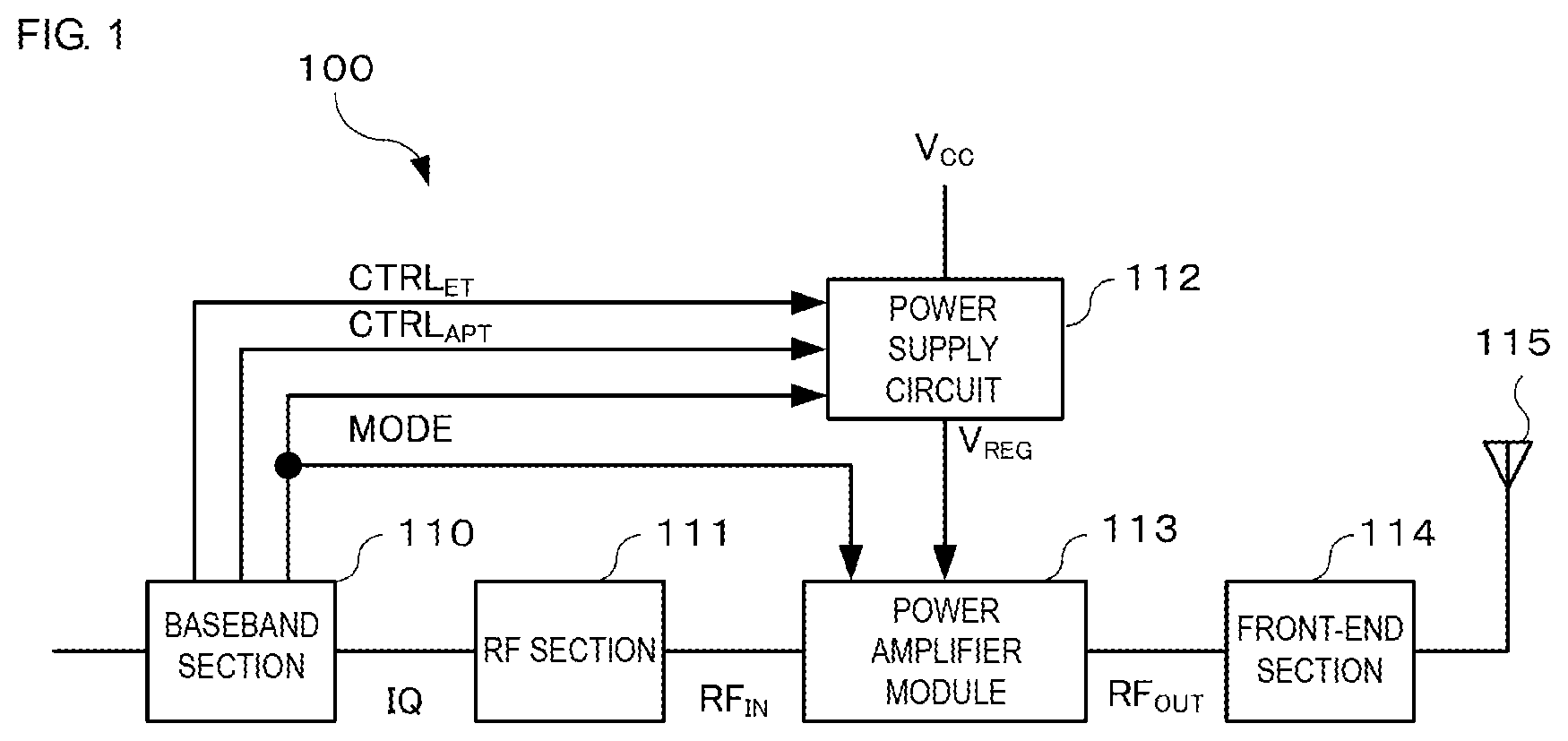
An embodiment of the present disclosure will be described below with reference to the accompanying drawings. FIG. 1 illustrates an example of the configuration of a transmitting unit 100 that includes a power amplifier module 113, which is an embodiment of the present disclosure. The transmitting unit 100 is used for transmitting various signals, such as audio and data signals, to a base station, in a mobile communication device, such as a cellular phone. The transmitting unit 100 supports multiple radio frequency (RF) bands (multiband). The mobile communication device also includes a receiving unit for receiving signals from a base station. However, an explanation of the receiving unit will be omitted.
As shown in FIG. 1, the transmitting unit 100 includes a baseband section 110, an RF section 111, a power supply circuit 112, a power amplifier module 113, a front-end section 114, and an antenna 115.
The baseband section 110 modulates an input signal, such as an audio signal or a data signal, on the basis of a modulation method, such as HSUPA or LTE, and outputs a modulation signal. In this embodiment, a modulation signal output from the baseband section 110 is an IQ signal (I (In-phase) signal and Q (Quadrature) signal) representing the amplitude and the phase on an IQ plane. The frequency of an IQ signal is, for example, about several MHz to several tens of MHz.
The baseband section 110 also outputs a mode signal MODE which specifies an operation mode of the power amplifier module 113. In this embodiment, the power amplifier module 113 is operable in the envelope tracking (ET) mode and the average power tracking (APT) mode. If the output of the power amplifier module 113 is a predetermined level or higher, the baseband section 110 outputs a mode signal MODE which specifies the ET mode. If the output of the power amplifier module 113 is lower than the predetermined level, the baseband section 110 outputs a mode signal MODE which specifies the APT mode.
The baseband section 110 also outputs a control signal for controlling the power supply voltage in accordance with the operation mode of the power amplifier module 113. More specifically, in the case of the ET mode, the baseband section 110 detects the amplitude level of a modulation signal on the basis of the IQ signal, and outputs a power supply control signal CTRL.sub.ET to the power supply circuit 112 so that a power supply voltage V.sub.REG to be supplied to the power amplifier module 113 will be at a level corresponding to the amplitude level of an RF signal. On the other hand, in the case of the APT mode, the baseband section 110 outputs a power supply control signal CTRL.sub.APT to the power supply circuit 112 so that a power supply voltage V.sub.REG to be supplied to the power amplifier module 113 will be at a level corresponding to the average power of the power amplifier module 113.
The RF section 111 generates an RF signal (RF.sub.IN) used for performing radio transmission from the IQ signal output from the baseband section 110. The frequency of the RF signal is about several hundreds of MHz to several GHz. In this case, instead of performing direct conversion from the IQ signal into the RF signal, the RF section 111 may first convert the IQ signal into an IF (Intermediate Frequency) signal and then convert the IF signal into the RF signal.
The power supply circuit 112 generates a power supply voltage V.sub.REG at a level corresponding to the operation mode, on the basis of the mode signal MODE and the power supply control signal CTRL.sub.ET or CTRL.sub.APT, and supplies the generated power supply voltage V.sub.REG to the power amplifier module 113. More specifically, in the case of the ET mode, the power supply circuit 112 generates a power supply voltage V.sub.REG (first power supply voltage) corresponding to the power supply control signal CTRL.sub.ET. In the case of the APT mode, the power supply circuit 112 generates a power supply voltage V.sub.REG (second power supply voltage) corresponding to the power supply control signal CTRL.sub.APT. The power supply circuit 112 may include a DC-to-DC converter which generates a power supply voltage V.sub.REG at a desired level from an input voltage (for example, a battery voltage V.sub.BAT).
The power amplifier module 113 amplifies power of the RF signal (RF.sub.IN) output from the RF section 111 to a level which is high enough to be transmitted to a base station, on the basis of the power supply voltage V.sub.REG supplied from the power supply circuit 112, and outputs an amplified signal (RF.sub.OUT).
The front-end section 114 performs filtering on the amplified signal (RF.sub.OUT) and switching between the amplified signal (RF.sub.OUT) and a signal received from a base station. The amplified signal output from the front-end section 114 is transmitted to the base station via the antenna 115.
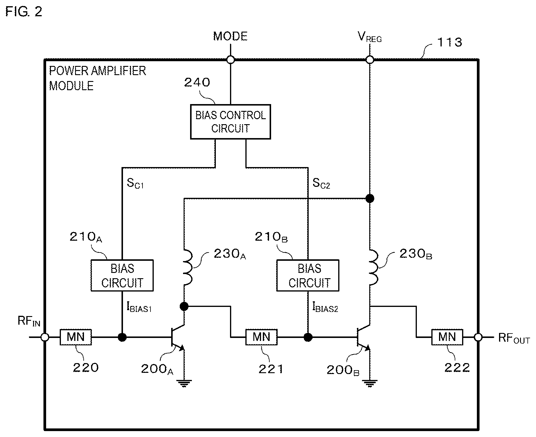
FIG. 2 illustrates an example of the configuration of the power amplifier module 113. As shown in FIG. 2, the power amplifier module 113 includes transistors 200.sub.A and 200.sub.B, bias circuits 210.sub.A and 210.sub.B, matching circuits 220, 221, and 222, inductors 230.sub.A and 230.sub.B, and a bias control circuit 240.
The transistors 200.sub.A and 200.sub.B form a two-stage amplifier, which amplifies an input RF signal (RF.sub.IN) and outputs an amplified signal (RF.sub.OUT). The transistors 200.sub.A and 200.sub.B are each constituted by a bipolar transistor, for example, a heterojunction bipolar transistor (HBT). The first-stage (driving-stage) transistor 200.sub.A amplifies the input RF signal (RF.sub.IN) and outputs the amplified signal. The second-stage transistor 200.sub.B amplifies the signal output from the transistor 200.sub.A and outputs the amplified signal. The number of stages of the amplifier is not restricted to two, and may be one or three or more.
The bias circuits 210.sub.A and 210.sub.B supply bias to the transistors 200.sub.A and 200.sub.B, respectively. The bias circuit 210.sub.A supplies a bias current I.sub.BIAS1 corresponding to a bias control signal S.sub.C1 output from the bias control circuit 240 to the transistor 200.sub.A. The bias circuit 210.sub.B supplies a bias current I.sub.BIAS2 corresponding to a bias control signal S.sub.C2 output from the bias control circuit 240 to the transistor 200.sub.B.
The matching circuits 220, 221, and 222 are disposed for performing impedance matching between circuits. The matching circuits 220, 221, and 222 are each constituted by, for example, inductors and capacitors.
The inductors 230.sub.A and 230.sub.B are disposed for the isolation of the RF signal. The power supply voltage V.sub.REG is supplied to the transistors 200.sub.A and 200.sub.B via the inductors 230.sub.A and 230.sub.B, respectively. In the power amplifier module 113 shown in FIG. 2, the power supply voltage V.sub.REG is supplied to both of the transistors 200.sub.A and 200.sub.B. However, the power supply voltage V.sub.REG may be supplied to only one of the transistors 200.sub.A and 200.sub.B, and a power supply voltage of a predetermined level, for example, the battery voltage V.sub.BAT, may be supplied to the other one of the transistors 200.sub.A and 200.sub.B.
The bias control circuit 240 outputs the bias control signals S.sub.C1 and S.sub.C2 to the transistors 200.sub.A and 200.sub.B, respectively, on the basis of the mode signal MODE so that bias to be supplied to the transistors 200.sub.A and 200.sub.B will be at a suitable level corresponding to the operation mode (ET/APT mode). The control operation using the bias control signals S.sub.C1 and S.sub.C2 will be discussed later. The bias control circuit 240 may be disposed outside of the power amplifier module 113.
FIG. 3 illustrates an example of the configuration of the bias circuits 210.sub.A and 210.sub.B. A bias circuit 210.sub.A1 includes transistors 300.sub.A_1 and 300.sub.A_2 (first and second transistors) and resistors 310.sub.A_1, 310.sub.A_2, 312.sub.A_1 (first resistor), and 312.sub.A_2 (second resistor). As shown in FIG. 3, the bias control signal S.sub.C1 output from the bias control circuit 240 includes bias control voltages V.sub.C1_1 and V.sub.C1_2 (first and second bias control voltages), and the bias control signal S.sub.C2 output from the bias control circuit 240 includes bias control voltages V.sub.C2_1 and V.sub.C2_2.
The transistors 300.sub.A_1 and 300.sub.A_2 are bipolar transistors, for example, HBTs. The bias control voltage V.sub.C1_1 is supplied to the base of the transistor 300.sub.A_1 via the resistor 310.sub.A_1. The bias control voltage V.sub.C1_2 is supplied to the base of the transistor 300.sub.A_2 via the resistor 310.sub.A_2. A power supply voltage of a predetermined level, for example the battery voltage V.sub.BAT, is supplied to the collectors of the transistors 300.sub.A_1 and 300.sub.A_2.
One end of the resistor 312.sub.A_1 is connected to the emitter of the transistor 300.sub.A_1 and the other end thereof is connected to the base of the transistor 200.sub.A. That is, the resistor 312.sub.A_1 is connected in series with the transistor 300.sub.A_1. One end of the resistor 312.sub.A_2 is connected to the emitter of the transistor 300.sub.A_2 and the other end thereof is connected to the base of the transistor 200.sub.A. That is, the resistor 312.sub.A_2 is connected in series with the transistor 300.sub.A_2. The resistance value R.sub.B1_1 of the resistor 312.sub.A_1 is different from the resistance value R.sub.B1_2 of the resistor 312.sub.A_2.
In the bias circuit 210.sub.A1, one of the transistors 300.sub.A_1 and 300.sub.A_2 is turned ON under the control of the bias control voltages V.sub.C1_1 and V.sub.C1_2. Then, the bias current I.sub.b--AS1 is output via one of the transistors 300.sub.A_1 and 300.sub.A_2 that is turned ON and the resistor 312.sub.A_1 or 312.sub.A_2 connected in series with this transistor. This control operation will be described below more specifically. For example, when the bias control voltage V.sub.C1_1 is at a high level and the bias control voltage V.sub.C1_2 is at a low level, the transistor 300.sub.A_1 is turned ON and the transistor 300.sub.A_2 is turned OFF. In this case, the bias circuit 210.sub.A1 outputs the bias current I.sub.BIAS1 determined by the bias control voltage V.sub.C1_1 and the resistance value R.sub.B1_1. When the bias control voltage V.sub.C1_1 is at a low level and the bias control voltage V.sub.C1_2 is at a high level, the transistor 300.sub.A_1 is turned OFF and the transistor 300.sub.A_2 is turned ON. In this case, the bias circuit 210.sub.A1 outputs the bias current I.sub.BIAS1 determined by the bias control voltage V.sub.C1_2 and the resistance value R.sub.B1_2.
The configuration of the bias circuit 210.sub.B1 is similar to that of the bias circuit 210.sub.A1. Elements of the bias circuit 210.sub.B1 equivalent to those of the bias circuit 210.sub.A1 are designated by like reference numerals, and an explanation thereof will be omitted. In the bias circuit 210.sub.B1, as well as in the bias circuit 210.sub.A1, the resistance value R.sub.B2_1 of the resistor 312.sub.B_1 is different from the resistance value R.sub.B2_2 of the resistor 312.sub.B_2.
In the bias circuit 210.sub.B1, for example, when the bias control voltage V.sub.C2_1 is at a high level and the bias control voltage V.sub.C2_2 is at a low level, the transistor 300.sub.B_1 is turned ON and the transistor 300.sub.B_2 is turned OFF. In this case, the bias circuit 210.sub.B1 outputs the bias current I.sub.BIAS2 determined by the bias control voltage V.sub.C2_1 and the resistance value R.sub.B2_1. When the bias control voltage V.sub.C2_1 is at a low level and the bias control voltage V.sub.C2_2 is at a high level, the transistor 300.sub.B_1 is turned OFF and the transistor 300.sub.B_2 is turned ON. In this case, the bias circuit 210.sub.B1 outputs the bias current I.sub.BIAS2 determined by the bias control voltage V.sub.C2_2 and the resistance value R.sub.B2_2.
In the power amplifier module 113, in the case of the ET mode, the bias control voltages V.sub.C1_1 and V.sub.C2_1 are made to have a high level, while the bias control voltages V.sub.C1_2 and V.sub.C2_2 are made to have a low level. In contrast, in the case of the APT mode, the bias control voltages V.sub.C1_1 and V.sub.C2_1 are made to have a low level, while the bias control voltages V.sub.C1_1 and V.sub.C2_2 are made to have a high level. With this control operation, the power amplifier module 113 is able to generate a bias current based on a suitable bias control voltage and a suitable resistance value corresponding to the operation mode. The value of the bias control voltage V.sub.C1_1 at a high level may be different from that of the bias control voltage V.sub.C1_2. For example, the bias control voltage V.sub.C1_1 at a high level (for example, about 2.85 V) may be higher than the bias control voltage V.sub.C1_2 at a high level (for example, about 2.8 V). The relationship between the bias control voltages V.sub.C2_1 and V.sub.C2_2 may be similar to that between the bias control voltages V.sub.C1_1 and V.sub.C1_2.
FIG. 4A is a graph illustrating an example of the relationship between the output level (dBm) and the power-added efficiency (%) when the power amplifier module 113 is operating in the ET mode. FIG. 4A shows a change in the power-added efficiency in accordance with the magnitudes of the bias control voltage V.sub.C (such as V.sub.C1_1 and V.sub.C1_2) and the resistance value R.sub.B (such as R.sub.B1_1 and R.sub.B1_2). In the ET mode, it is desirable to enhance the power-added efficiency. It is thus necessary to determine the bias control voltage V.sub.C and the resistance value R.sub.B so as to increase the power-added efficiency.
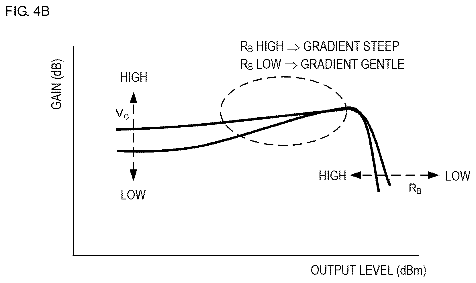
FIG. 4B is a graph illustrating an example of the relationship between the output level (dBm) and the gain (dB) when the power amplifier module 113 is operating in the APT mode. FIG. 4B shows a change in the gain in accordance with the magnitudes of the bias control voltage V.sub.C (such as V.sub.C1_1 and V.sub.C1_2) and the resistance value R.sub.B (such as R.sub.B1_1 and R.sub.B1_2) In the APT mode, it is desirable to enhance the linearity. It is thus necessary to determine the bias control voltage V.sub.C and the resistance value R.sub.B so as to obtain high linearity.
As shown in FIGS. 4A and 4B, the reference to be used for determining the bias control voltage V.sub.C and the resistance value R.sub.B in the case of the ET mode is different from that in the case of the APT mode. Accordingly, the bias control voltage V.sub.C and the resistance value R.sub.B suitable for one of the ET mode and the APT mode are not necessarily the same as the bias control voltage V.sub.C and the resistance value R.sub.B suitable for the other mode. In terms of this point, in the power amplifier module 113, in each of the bias circuits 210.sub.A1 and 210.sub.B1, the suitable bias control voltage V.sub.C (for example, V.sub.C1_1 or V.sub.C1_2) and the suitable resistance value R.sub.B (for example, R.sub.B1_1 or R.sub.B1_2) can be selected in accordance with the operation mode. In this manner, in a power amplifier module which is operable in multiple operation modes, it is possible to control bias to be supplied to an amplifier transistor.
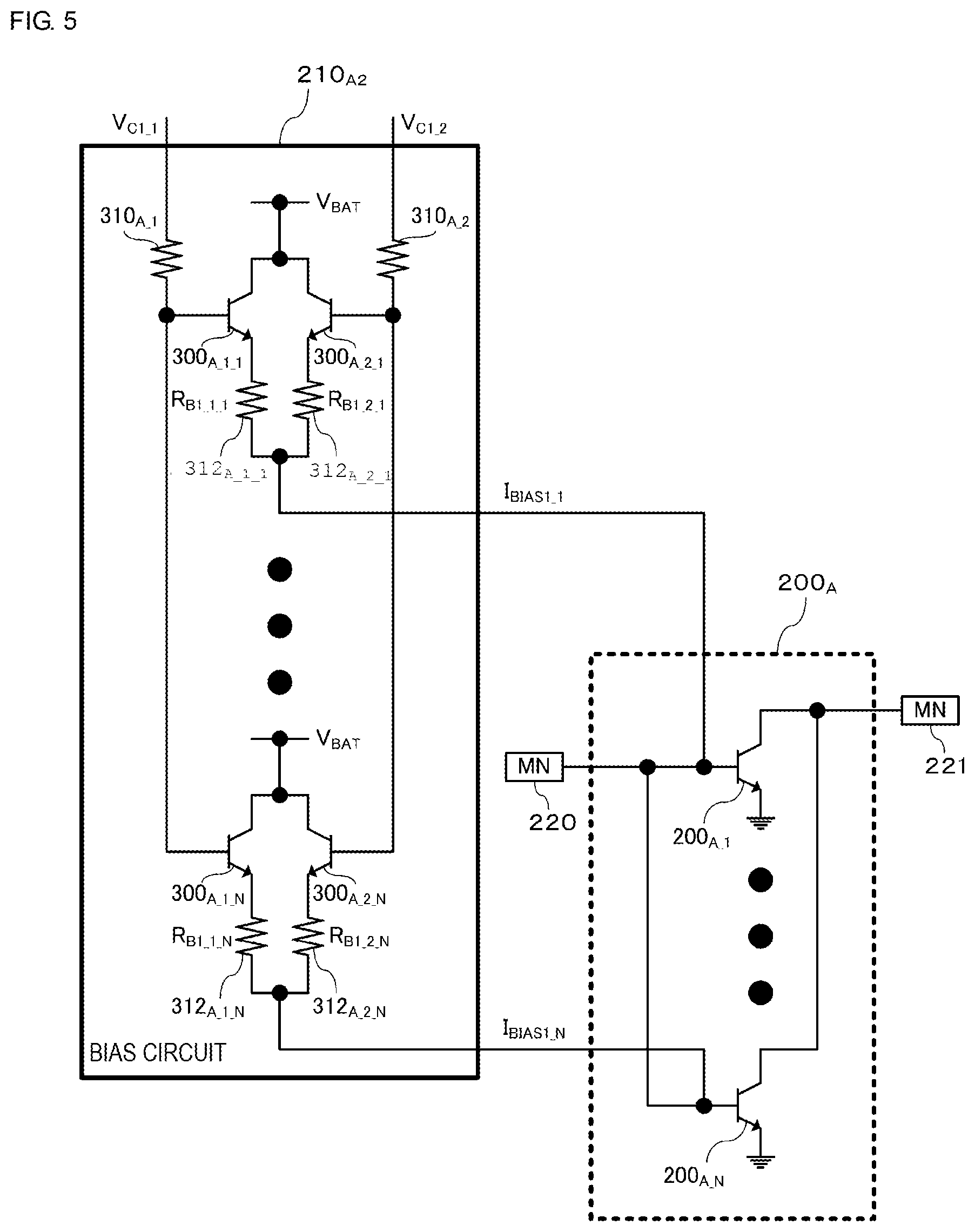
FIG. 5 illustrates an example of the configuration of the bias circuit 210.sub.A (210.sub.A2) when the amplifier transistor 200.sub.A is a multi-finger transistor. Elements equivalent to those of the bias circuit 210.sub.A1 are designated by like reference numerals, and an explanation thereof will be omitted. When the amplifier transistor 200.sub.B is a multi-finger transistor, the bias circuit 210.sub.B may be configured similarly to the bias circuit 210.sub.A.
In the example shown in FIG. 5, the transistor 200.sub.A is constituted by N unit transistors (fingers) 200.sub.A_1 through 200.sub.A_N connected in parallel with each other. The bias circuit 210.sub.A2 includes the same number of pairs of transistors 300.sub.A_1 and 300.sub.A_2 (that is, transistors 300.sub.A_1_1 through 300.sub.A_1_N and transistors 300.sub.A_2_1 through 300.sub.A_1_N, respectively) and the same number of pairs of resistors 312.sub.A_1 and 312.sub.A_2 (that is, resistors 312.sub.A_1_1 through 312.sub.A_1_N and resistors 312.sub.A_2_1 through 312.sub.A_2_N, respectively), which are provided in the bias circuit 210.sub.A1, as the number (N) of fingers.
In the bias circuit 210.sub.A2, for example, when the bias control voltage V.sub.C1_1 is at a high level and the bias control voltage V.sub.C1_2 is at a low level, the transistors 300.sub.A_1_1 through 300.sub.A_1_N are turned ON and the transistors 300.sub.A_2_1 through 300.sub.A_2_N are turned OFF. In this case, the bias circuit 210.sub.A2 outputs the bias current I.sub.BIAS1_k determined by the bias control voltage V.sub.C1_1 and the resistance value R.sub.B1_1_k to the transistor 200.sub.A_k (k=1 to N). When the bias control voltage V.sub.C1_1 is at a low level and the bias control voltage V.sub.C1_2 is at a high level, the transistors 300.sub.A_1_1 through 300.sub.A_1_N are turned OFF and the transistors 300.sub.A_2_1 through 300.sub.A_2_N are turned ON. In this case, the bias circuit 210.sub.A2 outputs the bias current I.sub.BIAS1_k determined by the bias control voltage V.sub.C1_2 and the resistance value R.sub.B1_2_k to the transistor 200.sub.A_k (k=1 to N). With this configuration, it is possible to obtain advantages similar to those achieved by the bias circuit 210.sub.A1.
FIG. 6 illustrates an example of the configuration of the bias circuit 210.sub.A (210.sub.A3) when the amplifier transistor 200.sub.A is a multi-finger transistor. Elements equivalent to those of the bias circuits 210.sub.A1 and 210.sub.A2 are designated by like reference numerals, and an explanation thereof will be omitted. When the amplifier transistor 200.sub.B is a multi-finger transistor, the bias circuit 210.sub.B may be configured similarly to the bias circuit 210.sub.A.
The bias circuit 210.sub.A3 shown in FIG. 6 includes the same number of resistors 312.sub.A_1 (that is, 312.sub.A_1_1 through 312.sub.A_1_N), which are provided in the bias circuit 210.sub.A1, as the number (N) of fingers.
In the bias circuit 210.sub.A3, for example, when the bias control voltage V.sub.C1_1 is at a high level and the bias control voltage V.sub.C1_2 is at a low level, the transistor 300.sub.A_1 is turned ON and the transistor 300.sub.A_2 is turned OFF. In this case, the bias circuit 210.sub.A3 outputs the bias current I.sub.BIAS1_k determined by the bias control voltage V.sub.C1_1 and the resistance value R.sub.B1_1_k to the transistor 200.sub.A_k (k=1 to N). When the bias control voltage V.sub.C1_1 is at a low level and the bias control voltage V.sub.C1_2 is at a high level, the transistor 300.sub.A_1 is turned OFF and the transistor 300.sub.A_2 is turned ON. In this case, the bias circuit 210.sub.A3 outputs the bias current I.sub.BIAS1_k determined by the bias control voltage V.sub.C1_2 and the resistance values R.sub.B1_2 and R.sub.B1_1_k to the transistor 200.sub.A_k (k=1 to N). With this configuration, it is possible to obtain advantages similar to those achieved by the bias circuit 210.sub.A1.
FIG. 7 illustrates an example of the configuration of the bias circuit 210.sub.A (210.sub.A4). Elements equivalent to those of the bias circuit 210.sub.A1 are designated by like reference numerals, and an explanation thereof will be omitted. The bias circuit 210.sub.3 may be configured similarly to the bias circuit 210.sub.A.
In the example shown in FIG. 7, the bias circuit 210.sub.A4 includes N pairs of transistors 300.sub.A_k and resistors 312.sub.A_k (N>2). In accordance with the N pairs of transistors 300.sub.A_k and resistors 312.sub.A_k, N bias control voltages (V.sub.C1_1 through V.sub.C1_N) are input from the bias control circuit 240 into the bias circuit 210.sub.A4.
In the bias circuit 210.sub.A4, for example, when the bias control voltage V.sub.C1_k is at a high level and the other bias control voltages are at a low level, among the transistors 300.sub.A_n (n=1 to N), the transistor 300.sub.A_k is turned ON and the other transistors are turned OFF. In this case, the bias circuit 210.sub.A4 outputs the bias current I.sub.BIAS1 determined by the bias control voltage V.sub.C1_k and the resistance value R.sub.B1_k to the transistor 200.sub.A (k=1 to N). With this configuration, it is possible to obtain advantages similar to those achieved by the bias circuit 210.sub.A1.
FIG. 8 illustrates an example of the configuration of the bias circuit 210.sub.A (210.sub.A5). Elements equivalent to those of the bias circuit 210.sub.A1 are designated by like reference numerals, and an explanation thereof will be omitted. The bias circuit 210.sub.B may be configured similarly to the bias circuit 210.sub.A.
The bias circuit 210.sub.A5 shown in FIG. 8 includes transistors 800.sub.A_1 and 800.sub.A_2 (first and second transistors) instead of the transistors 300.sub.A_1 and 300.sub.A_2 provided in the bias circuit 210.sub.A1. The bias circuit 210.sub.A5 also includes a transistor 810.sub.A (third transistor) and a resistor 820.sub.A (third resistor). In addition to the bias control voltages V.sub.C1_1 and V.sub.C1_2 (first and second bias control voltages), a bias control voltage V.sub.C1_3 (third bias control voltage) is also input from the bias control circuit 240 to the bias circuit 210.sub.A5.
The transistors 800.sub.A_1 and 800.sub.A_2 are field-effect transistors (FETs). The bias control voltage V.sub.C1_1 is supplied to the gate of the transistor 800.sub.A_1 via the resistor 310.sub.A_1. The bias control voltage V.sub.C1_2 is supplied to the gate of the transistor 800.sub.A_2 via the resistor 310.sub.A_2. The drains of the transistors 800.sub.A_1 and 800.sub.A_2 are connected to the emitter of the transistor 810.sub.A. The sources of the transistors 800.sub.A_1 and 800.sub.A_2 are connected to the resistors 312.sub.A_1 and 312.sub.A_2, respectively.
The transistor 810.sub.A is a bipolar transistor, for example, an HBT. The bias control voltage V.sub.C1_3 is supplied to the base of the transistor 810.sub.A via the resistor 820.sub.A. A power supply voltage of a predetermined level, for example the battery voltage V.sub.BAT, is supplied to the collector of the transistor 810.sub.A. The emitter of the transistor 810.sub.A is connected to the drains of the transistors 800.sub.A_1 and 800.sub.A_2. That is, the transistor 810.sub.A is connected in series with the transistors 800.sub.A_1 and 800.sub.A_2.
In the bias circuit 210.sub.A5, one of the transistors 800.sub.A_1 and 800.sub.A_2 is turned ON under the control of the bias control voltages V.sub.C1_1 and V.sub.C1_2. Additionally, in the bias circuit 210.sub.A5, under the control of the bias control voltage V.sub.C1_3, the currents to be supplied to the transistors 800.sub.A_1 and 800.sub.A_2 are controlled. For example, when the bias control voltage V.sub.C1_1 is at a high level and the bias control voltage V.sub.C1_2 is at a low level, the transistor 800.sub.A_1 is turned ON and the transistor 800.sub.A_2 is turned OFF. In this case, the bias circuit 210.sub.A5 outputs the bias current I.sub.BIAS1 determined by the bias control voltages V.sub.C1_1 and V.sub.C1_3 and the resistance value R.sub.B1_1. When the bias control voltage V.sub.C1_1 is at a low level and the bias control voltage V.sub.C1_2 is at a high level, the transistor 800.sub.A_1 is turned OFF and the transistor 800.sub.A_2 is turned ON. In this case, the bias circuit 210.sub.A5 outputs the bias current I.sub.BIAS1 determined by the bias control voltages V.sub.C1_2 and V.sub.C1_3 and the resistance value R.sub.B1_2. With this configuration, it is possible to obtain advantages similar to those achieved by the bias circuit 210.sub.A1.
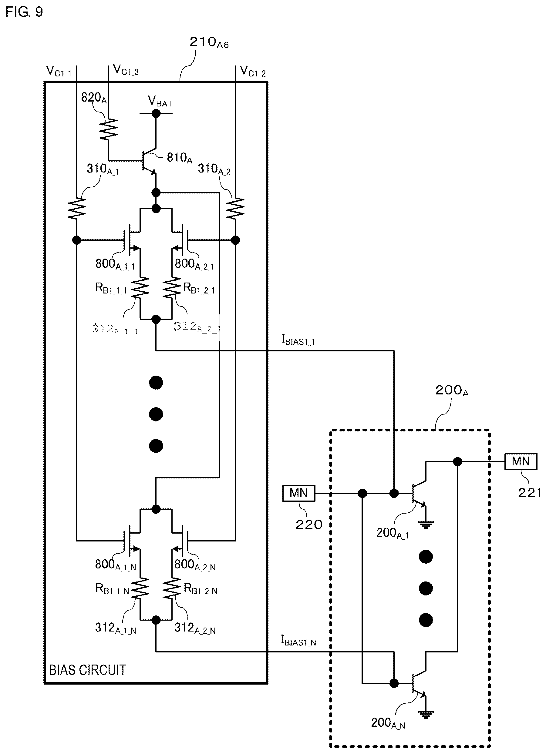
FIG. 9 illustrates an example of the configuration of the bias circuit 210.sub.A (210.sub.A6) when the amplifier transistor 200.sub.A is a multi-finger transistor. Elements equivalent to those of the bias circuits 210.sub.A2 and 210.sub.A5 are designated by like reference numerals, and an explanation thereof will be omitted. When the amplifier transistor 200.sub.B is a multi-finger transistor, the bias circuit 210.sub.B may be configured similarly to the bias circuit 210.sub.A.
The bias circuit 210.sub.A6 shown in FIG. 9 includes the same number of pairs of transistors 800.sub.A_1 and 800.sub.A_2 (that is, transistors 800.sub.A_1_1 through 800.sub.A_1_N and transistors 800.sub.A_2_1 through 800.sub.A_2_N, respectively) and the same number of pairs of resistors 312.sub.A_1 and 312.sub.A_2 (that is, resistors 312.sub.A_1_1 through 312.sub.A_1_N and resistors 312.sub.a_2_1 through 312 .sub.A_2_N, respectively), which are provided in the bias circuit 210.sub.A5, as the number (N) of fingers.
In the bias circuit 210.sub.A6, for example, when the bias control voltage V.sub.C1_1 is at a high level and the bias control voltage V.sub.C1_2 is at a low level, the transistor 800.sub.A_1_k is turned ON and the transistor 800.sub.A_2_k is turned OFF (k=1 to N). In this case, the bias circuit 210.sub.A6 outputs the bias current I.sub.BIAS1_k determined by the bias control voltages V.sub.C1_1 and V.sub.C1_3 and the resistance value R.sub.B1_1_k to the transistor 200.sub.A_k (k=1 to N). When the bias control voltage V.sub.C1_1 is at a low level and the bias control voltage V.sub.C1_2 is at a high level, the transistor 800.sub.A_1_k is turned OFF and the transistor 800.sub.A_2_k is turned ON (k=1 to N). In this case, the bias circuit 210.sub.A6 outputs the bias current I.sub.BIAS1_k determined by the bias control voltages V.sub.C1_2 and V.sub.C1_3 and the resistance value R.sub.B1_2_k to the transistor 200.sub.A_k (k=1 to N). With this configuration, it is possible to obtain advantages similar to those achieved by the bias circuit 210.sub.A1.
FIG. 10 illustrates an example of the configuration of the bias circuit 210.sub.A (210.sub.A7) when the amplifier transistor 200.sub.A is a multi-finger transistor. Elements equivalent to those of the bias circuits 210.sub.A3 and 210.sub.A5 are designated by like reference numerals, and an explanation thereof will be omitted. When the amplifier transistor 200.sub.B is a multi-finger transistor, the bias circuit 210.sub.B may be configured similarly to the bias circuit 210.sub.A.
The bias circuit 210.sub.A7 shown in FIG. 10 includes the same number of resistors 312.sub.A_1 (that is, 312.sub.A_1_N)through 312.sub.A_1_N), which are provided in the bias circuit 210.sub.A5, as the number (N) of fingers.
In the bias circuit 210.sub.A7, for example, when the bias control voltage V.sub.C1_1 is at a high level and the bias control voltage V.sub.C1_2 is at a low level, the transistor 800.sub.A_1 is turned ON and the transistor 800.sub.A_2 is turned OFF. In this case, the bias circuit 210.sub.A7 outputs the bias current I.sub.BIAS_k determined by the bias control voltages V.sub.C1_1 and V.sub.C1_3 and the resistance value R.sub.B1_1_k to the transistor 200.sub.A_k (k=1 to N). When the bias control voltage V.sub.C1_1 is at a low level and the bias control voltage V.sub.C1_2 is at a high level, the transistor 800.sub.A_1 is turned OFF and the transistor 800.sub.A_2 is turned ON. In this case, the bias circuit 210.sub.A7 outputs the bias current I.sub.BIAS1_k determined by the bias control voltages V.sub.C1_2 and V.sub.C1_3 and the resistance values R.sub.B1_2 and R.sub.B1_1_k to the transistor 200.sub.A_k (k=1 to N). With this configuration, it is possible to obtain advantages similar to those achieved by the bias circuit 210.sub.A1.
FIG. 11 illustrates an example of the configuration of the bias circuit 210.sub.A (210.sub.A8). Elements equivalent to those of the bias circuit 210.sub.A5 are designated by like reference numerals, and an explanation thereof will be omitted. The bias circuit 210.sub.B may be configured similarly to the bias circuit 210.sub.A.
The bias circuit 210.sub.A8 is a modified example of the bias circuit 210.sub.A5. In the bias circuit 210.sub.A8, resistors 312.sub.A_1 and 312.sub.A_2 connected in series with each other are connected to the emitter of the transistor 810.sub.A. The drain of the transistor 800.sub.A_1 is connected to one end of the resistor 312.sub.A_2 and the source thereof is connected to the other end of the resistor 312.sub.A_2. The drain of the transistor 800.sub.A_2 is connected to one end of the resistor 312.sub.A_1 and the source thereof is connected to the other end of the resistor 312.sub.A_1.
In the bias circuit 210.sub.A8, for example, when the bias control voltage V.sub.C1_1 is at a high level and the bias control voltage V.sub.C1_2 is at a low level, the transistor 800.sub.A_1 is turned ON and the transistor 800.sub.A_2 is turned OFF. In this case, the bias circuit 210.sub.A8 outputs the bias current I.sub.BIAS1 determined by the bias control voltages V.sub.C1_1 and V.sub.C1_3 and the resistance value R.sub.B1_1. When the bias control voltage V.sub.C1_1 is at a low level and the bias control voltage V.sub.C1_2 is at a high level, the transistor 800.sub.A_1 is turned OFF and the transistor 800.sub.A_2 is turned ON. In this case, the bias circuit 210.sub.A8 outputs the bias current I.sub.BIAS1 determined by the bias control voltages V.sub.C1_2 and V.sub.C1_3 and the resistance value R.sub.B1_2. With this configuration, it is possible to obtain advantages similar to those achieved by the bias circuit 210.sub.A1.
FIG. 12 illustrates an example of the configuration of the bias circuit 210.sub.A (210.sub.A9). Elements equivalent to those of the bias circuit 210.sub.A8 are designated by like reference numerals, and an explanation thereof will be omitted. The bias circuit 210.sub.B may be configured similarly to the bias circuit 210.sub.A.
The bias circuit 210.sub.A9 is a modified example of the bias circuit 210.sub.A8. The configuration of the bias circuit 210.sub.A9 is the same configuration as the bias circuit 210.sub.A8, except that bias circuit 210.sub.A9 does not include the resistor 310.sub.A_2 and the transistor 800.sub.A_2 provided in the bias circuit 210.sub.A8.
In the bias circuit 210.sub.A9, for example, when the bias control voltage V.sub.C1_1 is at a high level, the transistor 800.sub.A_1 is turned ON. In this case, the bias circuit 210.sub.A9 outputs the bias current I.sub.BIAS1 determined by the bias control voltage V.sub.C1_1 and the resistance value R.sub.B1_1. When the bias control voltage V.sub.C1_1 is at a low level, the transistor 800.sub.A_1 is turned OFF. In this case, the bias circuit 210.sub.A9 outputs the bias current I.sub.BIAS1 determined by the bias control voltage V.sub.C1_3 and the resistance values R.sub.B1_1 and R.sub.B1_2. With this configuration, it is possible to obtain advantages similar to those achieved by the bias circuit 210.sub.A1.
FIG. 13 illustrates an example of the configuration of the bias circuit 210.sub.A (210.sub.A10) when the amplifier transistor 200.sub.A is a multi-finger transistor. Elements equivalent to those of the bias circuits 210.sub.A7 and 210.sub.A9 are designated by like reference numerals, and an explanation thereof will be omitted. When the amplifier transistor 200.sub.B is a multi-finger transistor, the bias circuit 210.sub.B may be configured similarly to the bias circuit 210.sub.A.
The bias circuit 210.sub.A10 shown in FIG. 13 includes the same number of resistors 312.sub.A_1 (that is, 312.sub.A_1_1 through 312.sub.A_1_N), the resistor 312.sub.A_1 being provided in the bias circuit 210.sub.A9, as the number (N) of fingers.
In the bias circuit 210.sub.A10, for example, when the bias control voltage V.sub.C1_1 is at a high level, the transistor 800.sub.A_1 is turned ON. In this case, the bias circuit 210.sub.A10 outputs the bias current I.sub.BIAS1_k determined by the bias control voltage V.sub.C1_1 and the resistance value R.sub.B1_1_k to the transistor 200.sub.A_k (k=1 to N). When the bias control voltage V.sub.C1_1 is at a low level, the transistor 800.sub.A_1 is turned OFF. In this case, the bias circuit 210.sub.A10 outputs the bias current I.sub.BIAS1_2 determined by the bias control voltage V.sub.C1_3 and the resistance values R.sub.B1_2 and R.sub.B1_1_k to the transistor 200.sub.A_k (k=1 to N). With this configuration, it is possible to obtain advantages similar to those achieved by the bias circuit 210.sub.A1.
FIG. 14 illustrates an example of the configuration of the bias circuit 210.sub.A (210.sub.A11). Elements equivalent to those of the bias circuits 210.sub.A1 and 210.sub.A5 are designated by like reference numerals, and an explanation thereof will be omitted. The bias circuit 210.sub.B may be configured similarly to the bias circuit 210.sub.A.
The bias circuit 210.sub.A11 shown in FIG. 14 includes transistors 300.sub.A_1 and 300.sub.A_2 instead of the transistors 800.sub.A_1 and 800.sub.A_2 provided in the bias circuit 210.sub.A5.
The collector of the transistor 300.sub.A_1 is connected to the emitter of the transistor 810.sub.A via the resistor 312.sub.A_1 and the emitter thereof is connected to the transistor 200.sub.A. The collector of the transistor 300.sub.A_2 is connected to the emitter of the transistor 810.sub.A via the resistor 312.sub.A_2, and the emitter thereof is connected to the transistor 200.sub.A.
In the bias circuit 210.sub.A11, one of the transistors 300.sub.A_1 and 300.sub.A_2 is turned ON under the control of the bias control voltages V.sub.C1_1 and V.sub.C1_2. Additionally, in the bias circuit 210.sub.A11, under the control of the bias control voltage V.sub.C1_3, the currents to be supplied to the transistors 300.sub.A_1 and 300.sub.A_2 are controlled. For example, when the bias control voltage V.sub.C1_1 is at a high level and the bias control voltage V.sub.C1_2 is at a low level, the transistor 300.sub.A_1 is turned ON and the transistor 300.sub.A_2 is turned OFF. In this case, the bias circuit 210.sub.A11 outputs the bias current I.sub.BIAS1 determined by the bias control voltages V.sub.C1_1 and V.sub.C1_3 and the resistance value R.sub.B1_1. When the bias control voltage V.sub.C1_1 is at a low level and the bias control voltage V.sub.C1_2 is at a high level, the transistor 300.sub.A_1 is turned OFF and the transistor 300.sub.A_2 is turned ON. In this case, the bias circuit 210.sub.A11 outputs the bias current I.sub.BIAS1 determined by the bias control voltages V.sub.C1_2 and V.sub.C1_3 and the resistance value R.sub.B1_2. With this configuration, it is possible to obtain advantages similar to those achieved by the bias circuit 210.sub.A1.
FIG. 15 illustrates an example of the configuration of the bias circuit 210.sub.A (210.sub.A12). Elements equivalent to those of the bias circuit 210.sub.A8 are designated by like reference numerals, and an explanation thereof will be omitted. The bias circuit 210.sub.B may be configured similarly to the bias circuit 210.sub.A.
The bias circuit 210.sub.A12 is a modified example of the bias circuit 210.sub.A8. The bias circuit 210.sub.A12 includes transistors 300.sub.A_1 and 300.sub.A_2 instead of the transistors 800.sub.A_1 and 800.sub.A_2 provided in the bias circuit 210.sub.A8. The collector of the transistor 300.sub.A_1 is connected to one end of the resistor 312.sub.A_2 and the emitter thereof is connected to the other end of the resistor 312.sub.A_2. The collector of the transistor 300.sub.A_2 is connected to one end of the resistor 312.sub.A_1 and the emitter thereof is connected to the other end of the resistor 312.sub.A_1.
In the bias circuit 210.sub.A12, for example, when the bias control voltage V.sub.C1_1 is at a high level and the bias control voltage V.sub.C1_2 is at a low level, the transistor 300.sub.A_1 is turned ON and the transistor 300.sub.A_2 is turned OFF. In this case, the bias circuit 210.sub.A12 outputs the bias current I.sub.BIAS1 determined by the bias control voltages V.sub.C1_1 and V.sub.C1_3 and the resistance value R.sub.B1_1. When the bias control voltage V.sub.C1_1 is at a low level and the bias control voltage V.sub.C1_2 is at a high level, the transistor 300.sub.A_1 is turned OFF and the transistor 300.sub.A_2 is turned ON. In this case, the bias circuit 210.sub.A12 outputs the bias current I.sub.BIAS1 determined by the bias control voltages V.sub.C1_2 and V.sub.C1_3 and the resistance value R.sub.B1_2. With this configuration, it is possible to obtain advantages similar to those achieved by the bias circuit 210.sub.A1.
An exemplary embodiment of the disclosure has been discussed above. In the power amplifier module 113 including one of the bias circuits 210A.sub.1 through 210A.sub.8, 210A.sub.11, and 210A.sub.12, the ON state and the OFF state of two transistors are complementarily switched under the control of the bias control voltage V.sub.C1_1 supplied in a first operation mode (for example, the ET mode) and the bias control voltage V.sub.C1_2 supplied in a second operation mode (for example, the APT mode). Accordingly, the power amplifier module 113 is able to generate a bias current determined by the corresponding bias control voltage and resistance value based on the operation mode. It is thus possible to suitably control bias to be supplied to an amplifier transistor in a power amplifier module that is operable in multiple operation modes.
In the power amplifier module 113 including one of the bias circuits 210A.sub.5 through 210A.sub.8, 210A.sub.11, and 210A.sub.12, the ON state and the OFF state of two transistors are complementarily switched under the control of the bias control voltages V.sub.C1_1 and V.sub.C1_2, and also, the currents supplied to these transistors are controlled by using the bias control voltage V.sub.C1_3. Accordingly, the power amplifier module 113 is able to generate a bias current determined by the corresponding bias control voltages and resistance value based on the operation mode. It is thus possible to suitably control bias to be supplied to an amplifier transistor in a power amplifier module that is operable in multiple operation modes.
In the power amplifier module 113 including one of the bias circuits 210A.sub.9 and 210A.sub.10, the ON state and the OFF state of a transistor are switched under the control of the bias control voltage V.sub.C1_1 supplied in the first operation mode (for example, the ET mode), and also, the current supplied to this transistor is controlled by using the bias control voltage V.sub.C1_3. Accordingly, the power amplifier module 113 is able to generate a bias current determined by the corresponding bias control voltage and resistance value based on the operation mode. It is thus possible to suitably control bias to be supplied to an amplifier transistor in a power amplifier module that is operable in multiple operation modes.
The embodiment described above is provided for facilitating the understanding of the invention, but is not intended to be exhaustive or to limit the invention to the precise forms disclosed. Modifications and/or improvements may be made to the invention without departing from the scope and spirit of the invention, and equivalents of the invention are also encompassed in the invention. That is, suitable design changes made to the embodiment by those skilled in the art are also encompassed in the invention as long as they are within the scope and spirit of the invention. For example, the elements of the embodiment and the positions, materials, conditions, configurations, and sizes thereof are not restricted to those described in the embodiment and may be changed in an appropriate manner. The elements of the embodiment may be combined as long as such combinations are technically possible, and configurations obtained by combining the elements of the embodiment are also encompassed in the invention as long as they are within the scope and spirit of the invention.
While embodiments of the invention have been described above, it is to be understood that variations and modifications will be apparent to those skilled in the art without departing from the scope and spirit of the invention. The scope of the invention, therefore, is to be determined solely by the following claims.
* * * * *
D00000
D00001
D00002
D00003
D00004
D00005
D00006
D00007
D00008
D00009
D00010
D00011
D00012

D00013

D00014

D00015

D00016

XML
uspto.report is an independent third-party trademark research tool that is not affiliated, endorsed, or sponsored by the United States Patent and Trademark Office (USPTO) or any other governmental organization. The information provided by uspto.report is based on publicly available data at the time of writing and is intended for informational purposes only.
While we strive to provide accurate and up-to-date information, we do not guarantee the accuracy, completeness, reliability, or suitability of the information displayed on this site. The use of this site is at your own risk. Any reliance you place on such information is therefore strictly at your own risk.
All official trademark data, including owner information, should be verified by visiting the official USPTO website at www.uspto.gov. This site is not intended to replace professional legal advice and should not be used as a substitute for consulting with a legal professional who is knowledgeable about trademark law.