Electric dust collector and method of manufacturing the same
Jeon , et al. Feb
U.S. patent number 10,556,242 [Application Number 15/338,267] was granted by the patent office on 2020-02-11 for electric dust collector and method of manufacturing the same. This patent grant is currently assigned to LG ELECTRONICS INC.. The grantee listed for this patent is LG ELECTRONICS INC.. Invention is credited to Inho Choi, Jieun Choi, Hooncheol Jeon, Woongi Kil, Taeyoon Kim, Jongsu Lee, Kunyoung Lee, Kyoungho Lee, Yanghwa Lee, Hyungho Park, Sanghyuk Son.


View All Diagrams
| United States Patent | 10,556,242 |
| Jeon , et al. | February 11, 2020 |
Electric dust collector and method of manufacturing the same
Abstract
An electric dust collector is disclosed. The electric dust collector includes a film for collecting electrified dust particles and a case for receiving the film. A conductor-receiving part defining an insertion space, into which a portion of the film is inserted, is provided in the case. The electric dust collector further includes an electrode connection part filling the insertion space in the state of being in contact with the film. The electrode connection part is electrically connected to a voltage source to apply voltage in order to the film.
| Inventors: | Jeon; Hooncheol (Seoul, KR), Kim; Taeyoon (Seoul, KR), Lee; Yanghwa (Seoul, KR), Kil; Woongi (Seoul, KR), Park; Hyungho (Seoul, KR), Choi; Inho (Seoul, KR), Choi; Jieun (Seoul, KR), Lee; Kunyoung (Seoul, KR), Son; Sanghyuk (Seoul, KR), Lee; Jongsu (Seoul, KR), Lee; Kyoungho (Seoul, KR) | ||||||||||
|---|---|---|---|---|---|---|---|---|---|---|---|
| Applicant: |
|
||||||||||
| Assignee: | LG ELECTRONICS INC. (Seoul,
KR) |
||||||||||
| Family ID: | 57209388 | ||||||||||
| Appl. No.: | 15/338,267 | ||||||||||
| Filed: | October 28, 2016 |
Prior Publication Data
| Document Identifier | Publication Date | |
|---|---|---|
| US 20170120256 A1 | May 4, 2017 | |
Related U.S. Patent Documents
| Application Number | Filing Date | Patent Number | Issue Date | ||
|---|---|---|---|---|---|
| 62355118 | Jun 27, 2016 | ||||
| 62252017 | Nov 6, 2015 | ||||
| 62248463 | Oct 30, 2015 | ||||
Foreign Application Priority Data
| Nov 7, 2015 [KR] | 10-2015-0156254 | |||
| Dec 24, 2015 [KR] | 10-2015-0185846 | |||
| Mar 28, 2016 [KR] | 10-2016-0037235 | |||
| Mar 28, 2016 [KR] | 10-2016-0037246 | |||
| Current U.S. Class: | 1/1 |
| Current CPC Class: | B03C 3/86 (20130101); B03C 3/82 (20130101); B03C 3/45 (20130101); B03C 3/47 (20130101); B03C 3/02 (20130101); B03C 3/41 (20130101) |
| Current International Class: | F24F 6/04 (20060101); B03C 3/45 (20060101); B03C 3/82 (20060101); B03C 3/02 (20060101); B03C 3/41 (20060101); F24F 13/28 (20060101); F24F 13/20 (20060101); B01D 46/10 (20060101) |
References Cited [Referenced By]
U.S. Patent Documents
| 2364641 | December 1944 | Meston |
| 2873000 | February 1959 | Elam |
| 3665679 | May 1972 | McLain |
| 3685258 | August 1972 | Kostel |
| 8349052 | January 2013 | Noh |
| 8512455 | August 2013 | Yasuhiko |
| 8690996 | April 2014 | Ji |
| 9795971 | October 2017 | Shao |
| 101745462 | Jun 2010 | CN | |||
| 101884953 | Nov 2010 | CN | |||
| 202460831 | Oct 2012 | CN | |||
| 104575686 | Apr 2015 | CN | |||
| 2 532 434 | Dec 2012 | EP | |||
| 2 893 864 | Jun 2007 | FR | |||
| 2009-95799 | May 2009 | JP | |||
| 2009095799 | May 2009 | JP | |||
| 2010-131505 | Jun 2010 | JP | |||
| 20-1998-0058754 | Oct 1998 | KR | |||
| 10-2008-0055013 | Jun 2008 | KR | |||
| 10-2011-0088742 | Aug 2011 | KR | |||
| 10-2011-0088744 | Aug 2011 | KR | |||
| 10-2012-0136795 | Dec 2012 | KR | |||
Assistant Examiner: Turner; Sonji
Attorney, Agent or Firm: Dentons US LLP
Parent Case Text
CROSS-REFERENCE TO RELATED APPLICATIONS
This U.S. non-provisional patent application claims priority under 35 U.S.C. .sctn. 119 of U.S. Provisional Application No. 62/248,463, filed on Oct. 30, 2015, U.S. Provisional Application No. 62/252,017, filed on Nov. 6, 2015, Korean Patent Application No. 10-2015-0156254, filed on Nov. 7, 2015, Korean Patent Application No. 10-2015-0185846, filed on Dec. 24, 2015, Korean Patent Application No. 10-2016-0037235, filed on Mar. 28, 2016, Korean Patent Application No. 10-2016-0037246, filed on Mar. 28, 2016, U.S. Provisional Application No. 62/355,118, filed on Jun. 27, 2016, Korean Patent Application No. 10-2016-0083227, filed on Jul. 1, 2016, and Korean Patent Application No. 10-2016-0121745 filed on Sep. 22, 2016, the entire contents of which are hereby incorporated by reference.
Claims
What is claimed is:
1. An electric dust collector comprising: a film to collect electrified dust particles; and a case receiving the film, wherein the film comprises a conductive layer, to which voltage is applied, and an insulative layer covering the conductive layer, portion of the conductive layer exposed to form an exposed part, wherein the film comprises an insertion part extending from each of opposite ends thereof, wherein the exposed part is formed at the insertion parts, wherein a molding-receiving part defining a molding space into which the insertion parts are inserted, and a conductor-receiving part defining an insertion space into which the insertion parts are inserted, are provided in the case, and the electric dust collector further comprises an electrode connection part filling the insertion space in contact with the film, the electrode connection part electrically connected to a voltage source to apply voltage to the film, and an electrically insulative cover part filling the molding space in contact with the film while covering the electrode connection part.
2. The electric dust collector according to claim 1, wherein the electrode connection part is formed by hardening conductive paste.
3. The electric dust collector according to claim 2, wherein the conductive paste comprises a mixture of conductive powder, an organic solvent, and macromolecule resin.
4. The electric dust collector according to claim 1, wherein the electrode connection part is formed by combining conductive powder.
5. The electric dust collector according to claim 1, wherein the film comprises a plurality of films arranged to face each other such that gaps are formed between the respective films, and the electric dust collector further comprises a gap maintenance part having vertical bars inserted into the gaps to maintain the gaps.
6. The electric dust collector according to claim 1, wherein at least a portion of the exposed part is inserted into the insertion space to contact the electrode connection part.
7. The electric dust collector according to claim 1, wherein the conductor-receiving part and the exposed part are disposed in the molding space.
8. The electric dust collector according to claim 1, wherein the film is provided with a catching recess, and the molding-receiving part comprises a holding rib inserted into the catching recess to position the film.
9. The electric dust collector according to claim 6, wherein the electrode connection part fixes the exposed part.
10. The electric dust collector according to claim 1, wherein the film is provided with a catching recess, and the conductor-receiving part comprises a holding rib inserted into the catching recess so as to position the film.
11. The electric dust collector according to claim 1, further comprising a metal member disposed on a bottom surface of the conductor receiving part, and covered by the electrode connection part, a conducting wire electrically connected to the voltage source fixed to the metal member.
12. The electric dust collector according to claim 1, wherein the film comprises a plurality of films arranged to face each other such that a gap is formed between the respective films, wherein each of plurality of the films comprises the insertion parts extending from opposite ends thereof, in the longitudinal direction Y and bent in the lateral direction Z, and a catching recess formed in at least one end thereof in the longitudinal direction Y so as to be depressed in the lateral direction Z, wherein the conductor-receiving part comprises a conductor-receiving part holding rib inserted into the catching recess to position the film, wherein the molding-receiving part comprises a molding-receiving part holding rib inserted into the catching recesses to position the film, wherein the conductor-receiving part holding rib and the molding-receiving part holding rib overlap each other and inserted into the respective catching recesses, wherein the conductor receiving part holding rib comprises a first conductor receiving part holding rib inserted into a catching recess formed at a first end of each of the films and a second conductor receiving part holding rib inserted into a catching recess formed at a second end of each of the films, and wherein the molding-receiving part holding rib comprises a first molding-receiving part holding rib inserted into a catching recess formed at the first end of each of the films and a second molding-receiving part holding rib inserted into a catching recess formed at the second end of each of the films.
13. The electric dust collector according to claim 1, wherein the film comprises a plurality of films, and the electrode connection part electrically interconnects the films.
14. The electric dust collector according to claim 1, wherein the film comprises a plurality of first films, and a plurality of second films to which a low potential is applied as compared to the plurality of first films, the electrode connection part comprises a first electrode connection part to electrically interconnect the first films and a second electrode connection part to electrically interconnect the second films, and the conductor-receiving part comprises a first conductor-receiving part defining a space filled with the first electrode connection part and a second conductor-receiving part defining a space filled with the second electrode connection part.
15. The electric dust collector according to claim 14, wherein each of the first films and the second films includes a conductive layer, to which voltage is applied, and an insulative layer covering the conductive layer, a portion of the conductive layer exposed to form an exposed part, the exposed part of each of the first films is formed at a first end of the first film in a longitudinal direction, the exposed part of each of the second films is formed at a second end of the second film in the longitudinal direction, and opposite ends of the first films and the second films are fixed respectively to the first electrode connection part and the second electrode connection part.
16. A method of manufacturing the electric dust collector according to claim 2, the method comprising: disposing the film at a predetermined position; injecting the conductive paste such that a portion of the film is immersed in the conductive paste; and hardening the injected conductive paste.
Description
BACKGROUND OF THE INVENTION
1. Field of the Invention
The present invention relates to an electric dust collector for generating an electric field to collect electrified dust particles and a method of manufacturing the same.
2. Description of the Related Art
An air conditioner refers any of a cooler or a heater for controlling the temperature of air, an air freshener for removing foreign matter from air to maintain cleanliness of the air, a humidifier for supplying moisture to air, and/or a dehumidifier for removing moisture from air.
An electric dust collector is a stand-alone device or a device mounted in an air conditioner for electrifying and collecting dust particles in the air.
The electric dust collector generally includes an electrification unit for generating an electric field and a dust collection unit for collecting dust particles electrified by the electrification unit. While air passes through the dust collection unit after passing through the electrification unit, dust in the air is collected by the dust collection unit.
The electrification unit includes discharge films and opposite films arranged parallel to the discharge films. Dust is electrified as the result of corona discharge between the discharge films and the opposite films.
For example, Korean Patent Application Publication No. 10-2011-0088742 (published on Aug. 4, 2011) discloses a dust collection unit including film type first films and film type second films. Each first film is formed by applying insulative layers to opposite surfaces of an electrically conductive layer, and each second film is formed of a metal film sheet.
A plurality of film support parts are disposed at opposite sides of the first films and the second films, and protrusions are formed at the film support parts. The protrusions are inserted into gaps between the first films and the second films.
A film connection structure for applying high potential to each first film contacts a conductive layer exposed at one end of the first film, and a film connection structure for grounding each second film contacts the other end of the second film.
SUMMARY OF THE INVENTION
In the conventional art, the film connection structure contacts each first film and each second film, with the result that it is necessary to carefully perform the process. In addition, resistance is increased depending on the extent to which the film connection structure contacts each first film and each second film. Furthermore, sparks may occur when a voltage higher than a predetermined voltage is applied. It is an object of the present invention to solve this problem.
In the conventional art, the film connection structures or the exposed parts of the conductive layers of the first films may be wet after the electric dust collector is washed using water. When the electric dust collector is powered on in this state, a user may receive an electric shock, or the electric dust collector may be short-circuited. It is an object of the present invention to solve this problem.
In the conventional art, it is necessary to pay careful attention to the assembly of various engagement structures in order to maintain the distances between the respective films (e.g., the first films and the second films) and to attach the respective films (e.g., the first films and the second films). It is an object of the present invention to solve this problem.
In accordance with one aspect of the present invention, an electric dust collector includes a film to collect electrified dust particles and a case receiving the film. A conductor-receiving part defining an insertion space, into which a portion of the film is inserted, is provided in the case. The electric dust collector further includes an electrode connection part filling the insertion space in the state of being in contact with the film. The electrode connection part is electrically connected to a voltage source so as to apply voltage to the film.
The electrode connection part may be formed by hardening conductive paste. Alternatively, the electrode connection part may be formed by combining conductive powder.
The conductive powder may include conductive coating powder obtained by coating powder having relatively low electrical conductivity with a metal having relatively high electrical conductivity.
The film may include a plurality of films arranged to face each other such that gaps are formed between the respective films, and the electric dust collector may further include a gap maintenance part having vertical bars inserted into the gaps to maintain the gaps.
The film may include a conductive layer, to which voltage is applied, and an insulative layer covering the conductive layer. A portion of the conductive layer may be exposed to form an exposed part. At least a portion of the exposed part may be inserted into the insertion space to contact the electrode connection part.
The electric dust collector may further include an electrically insulative cover part covering the electrode connection part.
The electric dust collector may further include a molding-receiving part formed in the case, the molding-receiving part defining a molding space filled with the cover part.
The conductor-receiving part and the exposed part may be disposed in the molding space.
The film may be provided with a catching recess, and the molding-receiving part may include a holding rib inserted into the catching recess to position the film.
The film may be provided with a catching recess, and the conductor-receiving part may include a holding rib inserted into the catching recess to position the film.
The electric dust collector may further include a metal member covered by the electrode connection part in the state of being in contact with the electrode connection part, a conducting wire electrically connected to the voltage source being attached to the metal member.
Catching recesses are formed at opposite ends of each of the films in the longitudinal direction. The electric dust collector may further include a first holding rib inserted into the catching recess formed at one end of each of the films and a second holding rib inserted into the catching recess formed at the other end of each of the films.
The electrode connection part may electrically interconnect the films.
The film may include a plurality of first films, to which relatively high potential is applied, and a plurality of second films, to which relatively low potential is applied.
The electrode connection part may include a first electrode connection part to electrically interconnect the first films and a second electrode connection part to electrically interconnect the second films.
The conductor-receiving part may include a first conductor-receiving part defining a space filled with the first electrode connection part and a second conductor-receiving part defining a space filled with the second electrode connection part.
In accordance with one aspect of the present invention, an electric dust collector includes a plurality of films to collect electrified dust particles, a case receiving the films, and an electrode connection part to electrically interconnect the films. And, a conductor-receiving part defining an insertion space, into which a portion of each of the films is inserted, is provided in the case, the insertion space being filled with the electrode connection part.
In accordance with another aspect of the present invention, a method of manufacturing the electric dust collector according to the present invention includes disposing the film at a predetermined position, injecting the conductive paste such that a portion of the film is immersed in the conductive paste, and hardening the injected conductive paste.
BRIEF DESCRIPTION OF THE DRAWINGS
The above and other objects, features and other advantages of the present invention will be more clearly understood from the following detailed description taken in conjunction with the accompanying drawings, in which:
FIG. 1 is a sectional conceptual view showing an electric dust collector according to an embodiment of the present invention;
FIG. 2(a) is a conceptual view showing the discharge structure of an electrification unit shown in FIG. 1, wherein FIG. 2(a) is a view showing an electrification unit according to this embodiment and FIG. 2(b) is a view showing an electrification unit according to another embodiment;
FIG. 3 is a perspective view conceptually showing a circuit of the electrification unit shown in FIG. 1;
FIG. 4 is a sectional conceptual view showing an arrangement structure of films of a dust collection unit shown in FIG. 1;
FIG. 5 is an elevation view conceptually showing a circuit of the dust collection unit shown in FIG. 1;
FIG. 6 is a perspective view showing the structure of a film, more specifically, a view showing a first film;
FIG. 7 is a perspective view showing the structure of a film, more specifically, a view showing a second film;
FIG. 8 is a perspective view showing the external appearance of a case of the electric dust collector shown in FIG. 1, excluding a body;
FIG. 9 is a perspective view showing the electric dust collector shown in FIG. 8 when viewed from another side;
FIG. 10 is an exploded perspective view of the electric dust collector of FIG. 8 showing the state in which the electrification unit and an electrification unit case are assembled;
FIG. 11 is an elevation view showing the electrification unit and the electrification unit case of FIG. 10;
FIG. 12 is an exploded perspective view of the electric dust collector of FIG. 8 showing the state in which the dust collection unit and a dust collection unit case are assembled;
FIG. 13 is a perspective view showing the dust collection unit and the dust collection unit case of FIG. 12, excluding molding parts;
FIG. 14 is a sectional conceptual view showing an insertion space of a conductor-receiving part of FIG. 12 filled with an electrode connection part in the state in which a portion of the film is inserted in the insertion space of the conductor-receiving part, wherein FIG. 14(a) is a view of this embodiment and FIG. 14(b) is a view of another embodiment;
FIG. 15 is a perspective view showing the dust collection unit of FIG. 12, excluding the dust collection unit case;
FIG. 16 is an elevation view showing the dust collection unit case of FIG. 15, excluding the conductor-receiving part;
FIG. 17 is a perspective view showing the conductor-receiving part of FIG. 15;
FIG. 18 is a sectional view taken along line C1-C1' of FIG. 17;
FIG. 19 is a perspective view showing a metal member added to the conductor-receiving part of FIG. 17 in accordance with another embodiment;
FIG. 20 is a sectional view taken along line C2-C2' of FIG. 19;
FIG. 21 is an elevation view showing the electric dust collector shown in FIG. 8 when viewed from above;
FIG. 22 is a sectional view taken along line A1-A1' of FIG. 21;
FIG. 23 is a sectional view taken along line A2-A2' of FIG. 21;
FIG. 24 is a sectional view taken along line B-B' of FIG. 21;
FIG. 25 is an enlarged view showing a dotted-line part of FIG. 24;
FIG. 26 is an enlarged view showing a dotted-line part of FIG. 13;
FIG. 27 is a perspective view showing gap maintenance parts of FIG. 13;
FIG. 28 is an enlarged view showing a dotted-line part of FIG. 27;
FIG. 29 is an elevation view showing the gap maintenance parts of FIG. 27; and
FIG. 30 is an enlarged view showing a dotted-line part of FIG. 29.
DETAILED DESCRIPTION OF THE PREFERRED EMBODIMENTS
Exemplary embodiments of the present invention will be described with reference to the attached drawings.
In the drawings, the X-axis direction means the direction in which films of a dust collection unit, a description of which will follow, are alternately arranged, the Y-axis direction means the longitudinal direction of the films, and the Z-axis direction means the lateral direction of the films. In this embodiment, the X-axis direction, the Y-axis direction, and the Z-axis direction are perpendicular to each other. In this embodiment, the Z-axis direction is the upward-downward direction (specifically, the Z-axis direction indicated by the forward direction of the arrow is the upward direction and the Z-axis direction indicated by the reverse direction of the arrow is the downward direction). However, the present invention is not limited thereto.
In the following description, the term "potential" means electrical potential energy. In the following description, the term "voltage" means the potential difference between two points. In the following description, the term "electrical connection" includes connection between two members via another conductor as well as direct contact between the two members. In the following description, the terms "first," "second," etc. are used only to avoid confusion between components, and do not indicate the sequence or importance of the components.
An electric dust collector according to the present invention may be used as a component of an air conditioner or a vacuum cleaner that is capable of cooling, heating, freshening, or humidifying a room or as a stand-alone device.
In addition, the electric dust collector according to the present invention may have an integrated structure or a separable structure for easy cleaning. In the specification, an electric dust collector is described as being configured to have a structure in which a case, in which a dust collection unit is received, can be withdrawn from a body. However, the present invention is not limited thereto.
Hereinafter, a detachable electric dust collector 1 according to an embodiment of the present invention will be described with reference to FIG. 1.
The electric dust collector 1 includes an electrification unit 510 for electrifying dust particles in the air, a dust collection unit 540 for collecting the dust particles electrified by the electrification unit 510, and a case 501 and 502 for receiving the electrification unit 510 and the dust collection unit 540. The case 501 and 502 may define the external appearance of the electric dust collector 1. The electrification unit 510 may be disposed at the lower side, and the dust collection unit 540 may be disposed at the upper side.
The electric dust collector 1 may include a body 130 for supporting the case 501 and 502. The body 130 may be provided at one side thereof with a case insertion opening (not shown). The body 130 may have an inner space for receiving the case 501 and 502. The case 501 and 502 may be inserted into the inner space of the body 130 through the case insertion opening.
The case 501 and 502 is supported by the body 130. The case 501 and 502 may be separably located inside the body 130. The case 501 and 502 may be inserted into the body 130, and may be withdrawn from the body 130.
The body 130 may include a case guide 147 for guiding the location of the case 501 and 502 in the body 130. The body 130 may include a case guide 147 for guiding the withdrawal and introduction of the case 501 and 502 from and into the body 130. The case guide 147 may be disposed at each side of the case 501 and 502. The case guide 147 may be provided in the inner space of the body 130.
The case 501 and 502 may include an electrification unit case 501 for defining a space in which the electrification unit 510 is received and a dust collection unit case 502 for defining a space in which the dust collection unit 540 is received. The electrification unit case 501 may be disposed at the lower side thereof, and the dust collection unit case 502 may be disposed at the upper side thereof. The case 501 and 502 is formed such that the space for receiving the electrification unit 510 and the space for receiving the dust collection unit 540 communicate with each other.
In this embodiment, the electrification unit case 501 is disposed at the lower side thereof, and the dust collection unit case 502 is disposed at the upper side thereof. In addition, the electrification unit 510 is disposed at the lower side of the electrification unit 510, and the dust collection unit 540 is disposed at the upper side thereof. However, the present invention is not limited thereto.
The case 501 and 502 has an inlet port 506, through which air containing dust particles is introduced, and an outlet port 507, through which air in the case 501 and 502 is discharged to the outside. The case 501 and 502 may have a plurality of inlet ports 506. The case 501 and 502 may have a plurality of outlet ports 507. In this embodiment, the inlet port 506 is formed in the lower surface of the electrification unit case 501, and the outlet port 507 is formed in the upper surface of the dust collection unit case 502.
In this embodiment, the case 501 and 502 may be supported by the body 130 in the state in which the lower surface of the case 501 and 502 is spaced apart from the floor. In other embodiments, the case 501 and 502 may be provided with a case support member (not shown) for supporting the case 501 and 502 in the state in which the case 501 and 502 is spaced apart from the floor. The case support member may protrude in the downward direction of the case 501 and 502 so as to contact the floor.
In this embodiment, air flows in the direction denoted by reference symbol A. That is, air flows in the upward direction. Air is introduced into the case 501 and 502 through the inlet port 506. The air, introduced into the case 501 and 502 through the inlet port 506, sequentially passes through the electrification unit 510 and the dust collection unit 540, and is discharged to the outside through the outlet port 507. In other embodiments, air may flow in the downward direction, in the lateral direction, or in the diagonal direction. In other embodiments, the electrification unit 510 and the dust collection unit 540 may be disposed in the reverse arrangement. The electrification unit 510 and the dust collection unit 540 may be arranged horizontally. In this case, settings are performed such that air flows from the electrification unit 510 to the dust collection unit 540.
The electrification unit 510 according to this embodiment will be described with reference to FIGS. 2(a) and 3.
The electrification unit 510 includes a wire discharge film 521, to which high voltage is applied, and an opposite film plate 523 spaced apart from the wire discharge film 521. High voltage is applied to the wire discharge film 521 such that discharge can occur between the wire discharge film 521 and the opposite film plate 523.
A plurality of opposite film plates 523 may be disposed. The opposite film plates 523 may be spaced apart from each other so as to face each other in the state in which the wire discharge film 521 is disposed between the respective opposite film plates 523.
A plurality of wire discharge films 521 may be disposed. The wire discharge films 521 may be spaced apart from each other so as to be parallel to each other. The opposite film plates 523 may be disposed between the respective wire discharge films 521 in the direction perpendicular to the direction in which the wire discharge films 521 are arranged.
FIGS. 2(a) and 3 exemplarily show several wire discharge films 521 and several opposite film plates 523 alternately arranged while being spaced apart from each other in the direction X, which is perpendicular to the flow direction A of air. Alternatively, a larger number of wire discharge films 521 and opposite film plates 523 may be alternately arranged.
The wire discharge films 521 and the opposite film plates 523 may be attached to the electrification unit case 501. A distance-maintaining structure (not shown) for maintaining the distances between the wire discharge films 521 and the opposite film plates 523 may be provided.
When voltage is applied to the wire discharge films 521, corona discharge occurs between the wire discharge films 521 and the opposite film plates 523. Dust particles in the air are electrified while the air passes through the electrification unit 510.
An electrification unit 510' according to another embodiment will be described with reference to FIG. 2(b). The electrification unit 510' includes at least one ion generator 521' for generating ions. A plurality of ion generators 521' may be arranged at intervals in the direction X, which is perpendicular to the direction A in which air flows. The ion generators 521' may electrify dust particles in the air.
Each ion generator 521' includes a carbon fiber film 523' for performing corona discharge. The carbon fiber film 523' may be formed in the shape of a brush. The carbon fiber film 523' may be formed by binding a plurality of micro carbon fibers into a brush bundle. The carbon fiber film 523' may extend in the direction X, which is perpendicular to the direction A in which air flows.
Referring to FIG. 2(b), two ion generators 521a' and 521b' are arranged so as to be spaced apart from each other in the direction X, which is perpendicular to the direction A in which air flows. Carbon fiber films 523' protrude from the respective ion generators 521a' and 521b' so as to face each other.
When high voltage is applied to each carbon fiber film 523', the carbon fiber film 523' may be discharged to ionize molecules in the air. As a result, negative ions, such as OH- or O-, or positive ions, such as H+, may be generated. The ions generated by the carbon fiber film 523' electrify dust particles in the air. The negative ions may provide electrons to the dust particles such that the dust particles are electrified and act as a negative film. The positive ions may remove electrons from the dust particles such that the dust particles are electrified and act as a positive film.
Each ion generator 521' includes a film housing 525' for protecting a corresponding carbon fiber film 523'. The film housing 525' may be mounted in the electrification unit case 501. A printed circuit board (PCB) (not shown), to which the carbon fiber film 523' is connected, may be installed in the film housing 525'. The carbon fiber film 523' may be connected to the PCB via an additional wire. Alternatively, the carbon fiber film 523' may be directly connected to the PCB.
Referring to FIGS. 4 to 7, the dust collection unit 540 includes a film 540a for collecting the electrified dust particles. The dust collection unit 540 includes a plurality of films 540a for generating an electric field to collect the electrified dust particles.
In this embodiment, the films 540a may be formed by covering conductive layers 551a and 551b with insulative layers 552a and 552b, respectively. In other embodiments, conductive layers 551a may be formed on the surfaces of each film 540a. In particular, conductive layers 551a may be formed on the surfaces of each second film 542, to which low potential is applied.
The films 540a include a first film 541, to which relatively high potential is applied, and a second film 542, to which relatively low potential is applied.
A plurality of first films 541 may be provided. A plurality of second films 542 may be provided. The films 541 and 542 may be formed by applying insulative layers 552a and 552b to opposite surfaces of conductive layers 551a and 551b, respectively.
Each first film 541 may be formed by covering a conductive layer 551a, to which relatively high potential is applied, with insulative layers 552a. Each second film 542 may be formed by covering a conductive layer 551b, to which relatively low potential is applied, with insulative layers 552b.
The dust collection unit 540 includes a fixing part 540b for attaching the first films 541 and the second films 542 in the case 501 and 502. The fixing part 540b may attach the films 540a in the dust collection unit case 502.
The first films 541 and the second films 542 are alternately arranged. The first films 541 and the second films 542 are arranged such that the lateral direction Z of the films is the vertical direction. However, the present invention is not limited thereto. The first films 541 and the second films 542 may be arranged side by side so as to be aligned in the longitudinal direction Y.
The films 540a are arranged so as to face each other in the state in which gaps S are formed between the respective films. The first films 541 and the second films 542 are alternately arranged in the direction X, which is perpendicular to the lateral direction Z and the longitudinal direction Y in the state in which gaps S are formed between the respective films. Each of the films 540a is formed in the shape of a band that is longer in the longitudinal direction Y than in the lateral direction Z. The films 540a are arranged side by side so as to face each other in the state in which gaps S are formed between the respective films to constitute a film group.
Hereinafter, the circuit of the electric dust collector 1 will be described with reference to FIGS. 1, 3, and 5.
The body 130 includes power terminals 148a and 148b for respectively supplying power to the electrification unit 510 and the dust collection unit 540. The body 130 includes ground terminals 149a and 149b for respectively grounding the electrification unit 510 and the dust collection unit 540. An electrification unit power terminal 148a for supplying power to the electrification unit 510 and a dust collection unit power terminal 148b for supplying power to the dust collection unit 540 may be separately provided. An electrification unit ground terminal 149a for grounding the electrification unit 510 and a dust collection unit ground terminal 149b for grounding the dust collection unit 540 may be separately provided.
The body 130 includes a high-voltage generator 581 for generating high voltage. The body includes a high-voltage generator 581a for generating high voltage to be applied to the electrification unit 510. The body includes a high-voltage generator 581b for generating high voltage to be applied to the dust collection unit 540. The high-voltage generator 581b generates the potential difference between the first conductive layers 551a and the second conductive layers 551b.
In this embodiment, the high-voltage generator 581a and the high-voltage generator 581b constitute a single high-voltage generator 581. Power from the high-voltage generator 581 is applied to the electrification unit 510 and the dust collection unit 540 in parallel. The body 130 includes a power supply wire 585 for supplying power to the high-voltage generator 581.
The electric dust collector 1 includes power-receiving terminals 518 and 548 and ground-receiving terminals 519 and 549 that respectively contact the power terminals 148a and 148b and the ground terminals 149a and 149b.
The power terminals 148a and 148b, which are connected to the high-voltage generator 581 to respectively supply power to the electrification unit 510 and the dust collection unit 540, are disposed at the body 130. The ground terminals 149a and 149b, which are connected to a ground 582 to respectively ground the electrification unit 510 and the dust collection unit 540, are disposed at the body 130.
The power terminals 148a and 148b include an electrification unit power terminal 148a and a dust collection unit power terminal 148b. The ground terminals 149a and 149b include an electrification unit ground terminal 149a and a dust collection unit ground terminal 149b.
The electrification unit power terminal 148a, which is connected to the high-voltage generator 581a to supply power to the electrification unit 510, is disposed at the body 130. The dust collection unit power terminal 148b, which is connected to the high-voltage generator 581b to supply power to the dust collection unit 540, is disposed at the body 130. The electrification unit ground terminal 149a, which is connected to a ground 582a to ground the electrification unit 510, is disposed at the body 130. The dust collection unit ground terminal 149b, which is connected to a ground 582b to ground the dust collection unit 540, is disposed at the body 130.
The power-receiving terminals 518 and 548, which respectively contact the power terminals 148a and 148b to supply power to the electrification unit 510 and the dust collection unit 540, are disposed on the outer surface of the case 501 and 502. The ground-receiving terminals 519 and 549, which respectively contact the ground terminals 149a and 149b so as to ground the electrification unit 510 and the dust collection unit 540, are disposed on the outer surface of the case 501 and 502.
The power-receiving terminals 518 and 548 include an electrification unit power-receiving terminal 518 and a dust collection unit power-receiving terminal 548. The ground-receiving terminals 519 and 549 include an electrification unit ground-receiving terminal 519 and a dust collection unit ground-receiving terminal 549.
The electrification unit power-receiving terminal 518, which contacts the electrification unit power terminal 148a to supply power to the electrification unit 510, is disposed at the outer surface of the case 501 and 502. The dust collection unit power-receiving terminal 548, which contacts the dust collection unit power terminal 148b to supply power to the dust collection unit 540, is disposed at the outer surface of the case 501 and 502. The electrification unit ground-receiving terminal 519, which contacts the electrification unit ground terminal 149a to ground the electrification unit 510, is disposed at the outer surface of the case 501 and 502. The dust collection unit ground-receiving terminal 549, which contacts the dust collection unit ground terminal 149b to ground the dust collection unit 540, is disposed at the outer surface of the case 501 and 502.
The electrification unit power-receiving terminal 518 and the dust collection unit power-receiving terminal 548 may be disposed in the same horizontal plane so as to be spaced apart from each other diagonally. The electrification unit ground-receiving terminal 519 and the dust collection unit ground-receiving terminal 549 may be disposed in the same horizontal plane so as to be spaced apart from each other diagonally.
The case 501 and 502 may be introduced or inserted into the body 130. The case 501 and 502 may be withdrawn from the body 130. When the case 501 and 502 is introduced or inserted into the body 130, the power terminals 148a and 148b respectively contact the power-receiving terminals 518 and 548, and the ground terminals 149a and 149b respectively contact the ground-receiving terminals 519 and 549. Only in the state in which the case 501 and 502 is settled in the body 130, the power terminals 148a and 148b respectively contact the power-receiving terminals 518 and 548, and the ground terminals 149a and 149b respectively contact the ground-receiving terminals 519 and 549. The state in which the case 501 and 502 is settled in the body 130 means the state in which the case 501 and 502 is fully introduced or fully inserted into the body 130. That is, when the case 501 and 502 is not fully introduced or not fully inserted into the body 130 or the case 501 and 502 is withdrawn from the body 130, the case 501 and 502 is not settled in the body 130.
The electrification unit ground-receiving terminal 519 and the dust collection unit ground-receiving terminal 549 are respectively provided at points on the outer surface of the case 501 and 502 that correspond to the electrification unit ground terminal 149a and the dust collection unit ground terminal 149b.
On the outer surface of the case 501 and 502, the electrification unit power-receiving terminal 518 and the dust collection unit power-receiving terminal 548 may be opposite the electrification unit ground-receiving terminal 519 and a dust collection unit ground-receiving terminal 549. The power-receiving terminals 518 and 548 and the ground-receiving terminals 519 and 549 may be respectively disposed at the left and right side surfaces of the case 501 and 502. The electrification unit power-receiving terminal 518 and the dust collection unit power-receiving terminal 548 may be disposed at the same side surface of the case 501 and 502. The electrification unit ground-receiving terminal 519 and the dust collection unit ground-receiving terminal 549 may be disposed at the same side surface of the case 501 and 502.
Specifically, the power-receiving terminals 518 and 548 and the ground-receiving terminals 519 and 549 are disposed such that the power terminals 148a and 148b respectively contact the power-receiving terminals 518 and 548 and such that the ground terminals 149a and 149b respectively contact the ground-receiving terminals 519 and 549 only in the state in which the case 501 and 502 is settled in the body 130.
The electrification unit power terminal 148a and the dust collection unit power terminal 148b may be disposed on the same side of the inner surface of the body 130. The electrification unit ground terminal 149a and the dust collection unit ground terminal 149b may be disposed on the same side of the inner surface of the body 130.
In the state in which the case 501 and 502 is settled in the body 130, the electrification unit power terminal 148a contacts the electrification unit power-receiving terminal 518, and the electrification unit ground terminal 149a contacts the electrification unit ground-receiving terminal 519. As a result, high voltage is applied to the electrification unit 510.
In the state in which the case 501 and 502 is settled in the body 130, the dust collection unit power terminal 148b contacts the dust collection unit power-receiving terminal 548, and the dust collection unit ground terminal 149b contacts the dust collection unit ground-receiving terminal 549. As a result, high voltage is applied to the dust collection unit 540.
When the case 501 and 502 is withdrawn from the body 130, the electrification unit power terminal 148a is separated from the electrification unit power-receiving terminal 518, and the electrification unit ground terminal 149a is separated from the electrification unit ground-receiving terminal 519. As a result, the application of high voltage to the electrification unit 510 is interrupted.
When the case 501 and 502 is withdrawn from the body 130, the dust collection unit power terminal 148b is separated from the dust collection unit power-receiving terminal 548, and the dust collection unit ground terminal 149b is separated from the dust collection unit ground-receiving terminal 549. As a result, the application of high voltage to the dust collection unit 540 is interrupted.
The electric dust collector 1 includes a ground wire 583a for electrically interconnecting the opposite film plate 523 and the ground 582a. The electric dust collector includes a high-voltage wire 584a for electrically interconnecting the wire discharge film 521 and the high-voltage generator 581a. The high-voltage generator 581b may be configured such that the voltage difference between the first conductive layers 551a and the second conductive layers 551b is about 7 to 9 kV.
The electrification unit power terminal 148a and the electrification unit power-receiving terminal 518 are disposed on the high-voltage wire 584a. The electrification unit power terminal 148a and the electrification unit power-receiving terminal 518 function as a switch for electrically opening and closing the high-voltage wire 584a. The electrification unit ground terminal 149a and the electrification unit ground-receiving terminal 519 are disposed on the ground wire 583a. The electrification unit ground terminal 149a and the electrification unit ground-receiving terminal 519 function as a switch for electrically opening and closing the ground wire 583a.
The electric dust collector 1 includes a ground wire 583b for electrically interconnecting the second conductive layers 551b and the ground 582b. The electric dust collector 1 includes a high-voltage wire 584b for electrically interconnecting the first conductive layers 551a and the high-voltage generator 581b.
The dust collection unit power terminal 148b and the dust collection unit power-receiving terminal 548 are disposed on the high-voltage wire 584b. The dust collection unit power terminal 148b and the dust collection unit power-receiving terminal 548 function as a switch for electrically opening and closing the high-voltage wire 584b. The dust collection unit ground terminal 149b and the dust collection unit ground-receiving terminal 549 are disposed on the ground wire 583b. The dust collection unit ground terminal 149b and the dust collection unit ground-receiving terminal 549 function as a switch for electrically opening and closing the ground wire 583b.
The electric dust collector 1 includes a cutoff switch 145 for enabling or disabling the operation of the electric dust collector 1. The cutoff switch 145 may be disposed at the body 130. The cutoff switch 145 enables or disables the supply of power to the high-voltage generator 581. The cutoff switch 145 may enable or disable the supply of power to other parts of the electric dust collector 1 that need to receive power (e.g. a sensor and a display).
The cutoff switch 145 enables the operation of the electric dust collector 1 only in the state in which the case 501 and 502 is settled in the body 130. When the case 501 and 502 is separated from the body 130, the cutoff switch 145 disables the operation of the electric dust collector 1. The cutoff switch 145 disables the operation of the electric dust collector 1 in the state in which the case 501 and 502 is not fully coupled to the body 130 (i.e. the state in which the case 501 and 502 is not settled in the body 130).
The cutoff switch 145 is disposed on the power supply wire 585. The cutoff switch 145 enables or disables the supply of power to the high-voltage generators 581a and 581b. When the cutoff switch 145 is pushed, the power supply wire 585 may be short-circuited. When the cutoff switch 145 is not pushed, the power supply wire 585 may be open-circuited.
The cutoff switch 145 may be disposed at the inner surface of the body 130. The cutoff switch 145 may be disposed at the inner surface of the body 130 in the direction in which the case 501 and 502 is inserted into the body 130. The cutoff switch 145 may be configured to be pushed in the direction in which the case 501 and 502 is inserted into the body 130.
The case 501 and 502 includes a cutoff protrusion 144 for pushing the cutoff switch 145 (see FIGS. 8 and 9). The cutoff protrusion 144 is disposed at the side of the filter assembly 10 in the direction in which the case 501 and 502 is inserted into the body 130. The cutoff protrusion 144 protrudes in the direction in which the case 501 and 502 is inserted into the body 130.
The cutoff protrusion 144 is configured to push the cutoff switch 145 in the state in which the case 501 and 502 is settled in the body 130. When the cutoff protrusion 144 pushes the cutoff switch 145, the power supply wire 585 is short-circuited, whereby power may be supplied to the high-voltage generator 581. As a result, it is possible to prevent the user from receiving an electric shock when the user contacts the power terminals 148a and 148b and the ground terminals 149a and 149b in the state in which the case 501 and 502 is separated from, or not settled in, the body 130.
The electric dust collector 1 includes a short-circuit switch 600 configured such that the first conductive layers 551a and the second conductive layers 551b are short-circuited when it is turned ON and such that the first conductive layers 551a and the second conductive layers 551b are not short-circuited when it is turned OFF. Specifically, the first conductive layers 551a are connected to each other in parallel, and a short-circuit wire 600a is electrically connected to one end of the short-circuit switch 600 at the parallel connection point of the first conductive layers 551a. In addition, the second conductive layers 551b are connected to each other in parallel, and a short-circuit wire 600b is electrically connected to the other end of the short-circuit switch 600 at the parallel connection point of the second conductive layers 551b. The short-circuit switch 600 is disposed on the short-circuit wires 600a and 600b.
The short-circuit switch 600 is turned OFF in the state in which the case 501 and 502 is settled in the body 130. The short-circuit switch 600 is turned ON in the state in which the case 501 and 502 is separated from, or not settled in, the body 130.
In the state in which the case 501 and 502 is separated from, or not settled in, the body 130, the first conductive layers 551a and the second conductive layers 551b are short-circuited, whereby electric charge in the dust collection unit 540 is discharged. In the state in which the case 501 and 502 is settled in the body 130, the short-circuited state of the first conductive layers 551a and the second conductive layers 551b is released, whereby electric charge is formed in the dust collection unit 540 such that an electric field can be generated.
The body 130 includes a short-circuit protrusion (not shown) for pushing the short-circuit switch 600. The short-circuit protrusion is disposed at the side of the inner surface of the body 130 that faces the direction in which the case 501 and 502 is inserted into the body 130. The short-circuit protrusion protrudes in the direction in which the case 501 and 502 is withdrawn from the body 130.
The short-circuit switch 600 includes a pressurization part 626 exposed at the position corresponding to the short-circuit protrusion so as to be pushed in the state in which the case 501 and 502 is separated from, or not settled in, the body 130. The short-circuit switch 600 may include an elastic member (not shown) disposed at the side of the pressurization part 626 opposite the pressurization surface thereof. When the pressurization part 626 is pushed, the elastic member is elastically compressed. When the pushed state of the pressurization part 626 is released, the elastic member is restored.
A plurality of short-circuit switches 600 may be provided. The electric dust collector 1 may include a plurality of short-circuit switches 600.
The short-circuit switches 600 are connected to each other in parallel by the short-circuit wires 600a and 600b. When at least one of the short-circuit switches 600 is short-circuited, therefore, the first conductive layers 551a and the second conductive layers 551b are short-circuited. Even in the case in which one of the short-circuit switches 600 is not normally short-circuited due to the presence of foreign matter or breakage, therefore, the first conductive layers 551a and the second conductive layers 551b are short-circuited as long as at least another of the short-circuit switches 600 is normally short-circuited, thereby further improving the user's safety.
In this embodiment, the electric dust collector 1 includes two short-circuit switches 600-1 and 600-2. The short-circuit switches 600-1 and 600-2 may be arranged so as to be spaced apart from each other horizontally. The electric dust collector 1 may include a first short-circuit switch 600-1 and a second short-circuit switch 600-2.
The first short-circuit switch 600-1 includes a first pressurization part 652-1 disposed at the outer surface of the case 501 and 502. The second short-circuit switch 600-2 includes a second pressurization part 652-2 disposed at the outer surface of the case 501 and 502. The first short-circuit switch 600-1 and the second short-circuit switch 600-2 are arranged so as to be spaced apart from each other.
The body 130 includes a plurality of short-circuit protrusions (not shown) respectively formed at the positions corresponding to the pressurization parts 652-1 and 652-2. The short-circuit protrusions may include a first short-circuit protrusion (not shown) for pushing the first short-circuit switch 600-1 and a second short-circuit protrusion (not shown) for pushing the second short-circuit switch 600-2. In the state in which the case 501 and 502 is separated from, or not setted in, the body 130, the short-circuit protrusions push the pressurization parts 652-1 and 652-2, respectively.
Referring to FIGS. 8 and 9, the case 501 and 502 defines the external appearance of the electric dust collector 1. The case 501 and 502 includes a grip 503 for allowing the user to lift the case 501 and 502. The grip 503 may be formed at each of the opposite sides of the case 501 and 502. The grips 503 may be depressed in the case 501 and 502.
The case 501 and 502 has an inlet port 506 through which air is introduced to the electrification unit 510. The case 501 and 502 has an outlet port 507 through which air is discharged from the dust collection unit 540. A base gap maintenance part 561, a description of which will follow, may be disposed in the outlet port 507 so as to be exposed outward.
The case 501 and 502 has a drainage hole 508, through which water, introduced into the case 501 and 502 for washing, is drained from the case 501 and 502. A plurality of drainage holes 508 may be provided. The drainage holes 508 may be arranged so as to be spaced apart from each other.
The drainage holes 508 may be formed in the sides of the outer surface of the case 501 and 502 in which the inlet port 506 is formed so as to be spaced apart from the inlet port 506. The drainage holes 508 may be formed in the opposite sides of the outer surface of the case 501 and 502 in the longitudinal direction Y of the opposite film plates 523. The drainage holes 508 may be formed in the opposite sides of the outer surface of the case 501 and 502 in the longitudinal direction Y of the films 540a.
Referring to FIGS. 10 and 11, the electrification unit 510 includes a wire discharge film 521, to which high voltage is applied, and an opposite film plate 523 spaced apart from the wire discharge film 521.
When voltage is applied to the wire discharge film 521, corona discharge occurs between the wire discharge film 521 and the opposite film plate 523. As a result, molecules in the air may be ionized, whereby negative ions, such as OH- or O-, or positive ions, such as H+, may be generated. The generated ions electrify dust particles in the air. The negative ions may provide electrons to the dust particles such that the dust particles are electrified and act as a negative film. The positive ions may remove electrons from the dust particles such that the dust particles are electrified and act as a positive film.
A plurality of opposite film plates 523 may be disposed. The opposite film plates 523 may be spaced apart from each other so as to face each other in the state in which the wire discharge film 521 is disposed between the respective opposite film plates 523.
The opposite ends of the opposite film plates 523 may be connected to each other via the film plate connection parts 524. The film plate connection parts 524 are disposed in the horizontal plane, and the opposite film plates 523 are disposed in the plane perpendicular to the film plate connection parts 524.
The film plate connection parts 524 and the opposite film plates 523 may be integrally formed by incising the middle part of a metal sheet and bending the incised middle part by 90 degrees. Specifically, the film plate connection parts 524 and the opposite film plates 523 may be integrally formed as follows. The middle part of a metal sheet is incised to a length equal to that of the long side of each of the opposite film plates 523, excluding the opposite ends of the metal sheet, which will serve as the film plate connection parts 524. The opposite ends of the middle part of the metal sheet, incised to the length equal to that of the long side of each of the opposite film plates 523, are incised to a length equal to that of the short side of each of the opposite film plates 523 so as to be perpendicular to the incised middle part. The part of the metal sheet incised in a bracket shape (i.e. the middle part incised to the length equal to that of the long side of each of the opposite film plates 523 and the opposite ends of the middle part incised to the length equal to that of the short side of each of the opposite film plates 523 so as to be perpendicular to the incised middle part) is bent by 90 degrees. The bent part becomes a corresponding one of the opposite film plates 523.
A plurality of wire discharge films 521 may be disposed. The wire discharge films 521 may be spaced apart from each other so as to be parallel to each other. The opposite film plates 523 may be disposed between the respective wire discharge films 521 so as to be parallel to the wire discharge films 521.
The wire discharge films 521 may be connected to each other in series. That is, the wire discharge films 521 may be constituted by a single wire member. In this embodiment, a single wire member extends from one one-side wire support part 522a to one opposite-side wire support part 522b so as to constitute a wire discharge film 521. The wire member extends from the one opposite-side wire support part 522b to another opposite-side wire support part 522b adjacent to the one opposite-side wire support part 522b so as to constitute a wire series connection part (not shown). The wire member extends from the another opposite-side wire support part 522b to another one-side wire support part 522a adjacent to the one one-side wire support part 522a so as to constitute another wire discharge film 521. In this way, the wire discharge films 521 are connected to the wire series connection parts via the wire support parts 522a and 522b, which are disposed at opposite sides so as to be spaced apart from each other by a predetermined distance.
Each of the wire support parts 522 includes a vertical member extending in the air flow direction. The wire member may be bent at the vertical member while being supported by the vertical member.
In this embodiment, a plurality of wire discharge films 521 and a plurality of opposite film plates 523 are alternately arranged so as to be spaced apart from each other in the direction X perpendicular to the air flow direction A. The wire discharge films 521 and the opposite film plates 523 are disposed at the downstream side of the inlet port 506.
The film plate connection parts 524 are disposed at the opposite ends of the opposite film plates 523 so as to extend in the direction X, which is perpendicular to the opposite film plates 523. The wire series connection parts are disposed at the opposite ends of the wire discharge films 521 so as to extend in the direction X, which is perpendicular to the wire discharge films 521.
The wire discharge films 521 may be disposed between the respective opposite film plates 523 so as to be adjacent to the upstream sides thereof. The wire series connection parts may be disposed in the same plane as the wire discharge films 521. The film plate connection parts 524 may be disposed in the plane at the downstream sides of the opposite film plates 523 such that the wire series connection parts are spaced further apart from the film plate connection parts 524. The reason for this is that it is necessary to reduce the possibility of sparks occurring between the wire series connection parts and the film plate connection parts 524, since high voltage is also applied to the wire series connection parts and the film plate connection parts 524 are also made of a metal material and are electrically connected to the opposite film plates 523.
The wire discharge films 521 and the opposite film plates 523 are attached to the electrification unit case 501. The opposite ends of the portion of the wire member corresponding to each of the wire discharge films 521 are attached to the electrification unit case 501. High voltage is applied to the portion of the wire member via the fixed ends thereof.
The electrification unit 510 includes a spark prevention part 525 attached to the electrification unit case 501 for supporting the opposite film plates 523. The spark prevention part 525 attaches the film plate connection parts 524.
The spark prevention part 525 is disposed at each end of each of the opposite film plates 523. The spark prevention part 525 includes a shielding member (not shown) interposed between each of the film plate connection parts 524, which are disposed so as to be vertically spaced apart from each other, and a corresponding one of the wire series connection parts. The shielding member may be made of an insulative material. The shielding member reduces the likelihood of sparks occurring between each of the wire series connection parts and a corresponding one of the film plate connection parts 524.
The spark prevention part 525 is provided with a recess, into which each of the film plate connection parts 524 is inserted. The recess, into which each of the film plate connection parts 524 is inserted, is depressed in the longitudinal direction of the opposite film plates 523. The member having the recess, into which each of the film plate connection parts 524 is inserted, surrounds the upper surface and the lower surface of each of the film plate connection parts 524. The member for surrounding the lower surface of each of the film plate connection parts 524 may be embodied by the shielding member.
Referring to FIGS. 12 and 13, the dust collection unit 540 includes a film 540a for collecting electrified dust particles. A plurality of films 540a may be provided. The dust collection unit 540 includes a plurality of films 540a for collecting electrified dust particles.
The dust collection unit 540 includes a fixing part 540b for attaching the film 540a in the case 501 and 502. The film 540a is received in the case 501 and 502. A plurality of films 540a may be received in the case 501 and 502. The fixing part 540b may attach the films 540a in the dust collection unit case 502.
The films 540a may be arranged so as to face each other in the state in which gaps S are formed between the respective films. Each of the films 540a is formed in the shape of a band that is longer in the longitudinal direction Y than in the lateral direction Z. The films 540a are arranged side by side so as to face each other in the state in which gaps S are formed between the respective films to constitute a film group. The films 540a are disposed such that one side of each of the films 540a in the lateral direction Z faces the outlet port 507.
The films 540a include a plurality of first films 541, to which relatively high potential is applied, and a plurality of second films 542, to which relatively low potential is applied. The first films 541 and the second films 542 are alternately arranged. The first films 541 and the second films 542 are alternately arranged so as to face each other in the state in which gaps S are formed between the respective films.
The fixing part 540b includes gap maintenance parts 560 disposed on at least one of the lateral opposite sides of the film group for maintaining the gap S.
The gap maintenance parts 560 are attached in the case 501 and 502. In this embodiment, the gap maintenance parts 561 and 566 are attached only to the dust collection unit case 502. The gap maintenance parts 560 may also support the films 540a.
The gap maintenance parts 560 may include roof gap maintenance parts 566, which are disposed at one of the opposite sides of the film group in the lateral direction Z that is distant from the inner surface of the dust collection unit case 502. The gap maintenance parts 560 may include base gap maintenance parts 561, disposed at one side of the film group in the lateral direction Z, and roof gap maintenance parts 566, disposed at the other side of the film group in the lateral direction Z.
The fixing part 540b includes molding parts 578 and 579 that fill a predetermined space 576 in the state in which a portion of each of the films 540a is inserted in the space 576. The molding parts 578 and 579 attach the films 540a via hardening of predetermined paste. The molding parts 578 and 579 are formed by hardening the paste in the state in which a portion of each of the films 540a is immersed in the paste.
The films 540a are arranged such that the lateral direction Z of the films is the upward-downward direction. However, the present invention is not limited thereto. The films 540a may be arranged side by side so as to be aligned in the longitudinal direction Y. The films 540a are arranged such that gaps S are formed between the respective films in the direction X, which is perpendicular to both the lateral direction Z and the longitudinal direction Y.
Referring to FIGS. 6 and 7, each of the first films 541 and the second films 542 is formed in the shape of a band. The length of the first film 541 and the second film 542 may be about 200 to 250 mm. The first film 541 and the second film 542 may be formed in the shape of a flat plate. At least a portion of the first film 541 and the second film 542 may be curved in the direction X.
The conductive layers 551a and 551b of the films 540a may be made of a carbon material. The conductive layers 551a and 551b may have a thickness of 10 to 100 um. The conductive layer 551a of each first film 541 constitutes a high-potential electrode, and the conductive layer 551b of each second film 542 constitutes a low-potential electrode.
The insulative layers 552a and 552b respectively cover the conductive layers 551a and 551b, excluding exposed parts 557 and 558. The insulative layers 552a and 552b may be made of a material, such as polypropylene (PP), polyethylene terephthalate (PET), polyethylene naphthalate (PEN), or polyurethene (PU), containing a nano-filler, such as TiO.sub.2, Al.sub.2O.sub.3, or SiO.sub.2. The insulative layers 552a and 552b may have a thickness of 100 to 1500 um.
The conductive layer 551a may be patterned on one surface of one of the insulative layers 552a by screen printing, and the other of the insulative layers 552a may be attached to the one of the insulative layers 552a while covering the pattern excluding a portion of the pattern. In the same manner, the conductive layer 551b may be patterned on one surface of one of the insulative layers 552b by screen printing, and the other of the insulative layers 552b may be attached to the one of the insulative layers 552b while covering the pattern excluding a portion of the pattern.
The films 540a include exposed parts 557 and 558, through which portions of the conductive layers 551a and 551b are exposed. Portions of the conductive layers 551a and 551b of the films 540a are exposed to the outside, and the remainders of the conductive layers 551a and 551b of the films 540a are covered by the insulative layers 552a and 552b.
When relatively high potential is applied to the first conductive layer 551a and relatively low potential is applied to the second conductive layer 551b, an electric field is generated between the conductive layers 551a and 551b. Dust particles electrified by the electrification unit 510 receive electric force in the electric field depending upon the electrified polarity thereof. As a result, the dust particles stick to a corresponding one of the insulative layers 552a of the first film 541 or a corresponding one of the insulative layers 552b of the second film 542.
Each film 540a includes an insertion part 555 extending from at least one end thereof in the longitudinal direction Y so as to be inserted into the space 576. The insertion part 555 may be formed at each end of each of the first films 541 and the second films 542 in the longitudinal direction Y.
Referring to FIGS. 13 and 14(a), the insertion part 555 according to this embodiment extends from at least one end of each film in the longitudinal direction Y and is bent in the lateral direction Z. The films 540a include insertion parts 555 extending from opposite ends thereof in the longitudinal direction Y and bent in the lateral direction Z. An insertion port of an insertion space 576a of a conductor-receiving part 571, a description of which will follow, is formed so as to face the direction in which the insertion parts 555 are bent. The films 540a have catching recesses 556, a description of which will follow. Holding ribs 572, a description of which will follow, are inserted into the catching recesses 556.
Referring to FIG. 14(b), an insertion part 555' according to another embodiment extends from at least one end of each film in the longitudinal direction Y. A plurality of films 540a' includes insertion parts 555' extending from opposite ends thereof in the longitudinal direction Y. An insertion port of an insertion space 576a' of a conductor-receiving part 571' is formed so as to face the direction in which the insertion parts 555 extend. The films 540a' may have no catching recesses 556.
The exposed parts 557 and 558 are formed at the insertion parts 555. The films 540a include insertion parts 555a having exposed parts 557 and 558. The films 540a may further include insertion parts 555b having no exposed parts 557 and 558. One of the films 540a may include an insertion part 555a formed at one end thereof in the longitudinal direction Y and an insertion part 555b formed at the other end thereof in the longitudinal direction Y.
The exposed part 557 formed at each of the first films 541 is disposed at one end of the first film 541 in the longitudinal direction Y. The exposed part 558 formed at each of the second films 542 is disposed at the other end of the second film 542 in the longitudinal direction Y. In this case, the insertion part 555a may be formed at one end of the first film 541 in the longitudinal direction Y, and the insertion part 555b may be formed at the other end of the first film 541 in the longitudinal direction Y. In addition, the insertion part 555b may be formed at one end of the second film 542 in the longitudinal direction Y, and the insertion part 555a may be formed at the other end of the second film 542 in the longitudinal direction Y.
Each of the first films 541 is configured such that the conductive layer 551a is exposed only at the insertion part 555a formed at one end thereof. Each of the second films 542 is configured such that the conductive layer 551b is exposed only at the insertion part 555a formed at the other end thereof. The high-potential connection part 557 provided at each of the first films 541 is formed only at the insertion part 555a formed at one end thereof. The low-potential connection part 558 provided at each of the second films 542 is formed only at the insertion part 555a formed at the other end thereof.
Each of the films 540a has a catching recess 556 formed in at least one end thereof in the longitudinal direction Y so as to be depressed in the lateral direction Z. The catching recess 556 may be formed in each end of each of the films 540a in the longitudinal direction Y.
One surface of the insertion part 555 may define one surface of the catching recess 556. The catching recess 556 may be formed in the shape of a slit that is open at one side thereof.
The case 501 and 502 includes holding ribs 572, which are inserted into the respective catching recesses 556. The holding ribs 572 may be coupled to the dust collection unit case 502.
The holding ribs 572 are engaged into the catching recess 556. The holding ribs 572 protrude from the dust collection unit case 502 toward the catching recess 556. The holding ribs 572 may extend in the direction X in which the films are arranged, a detailed description of which will follow.
At least one of the opposite ends of the films 540a in the longitudinal direction Y may be formed so as to have a relatively small length in the lateral direction Z. At least one of the opposite ends of the films 540a in the longitudinal direction Y is formed such that one end of each of the films in the lateral direction Z further extends in the longitudinal direction Y. In the state in which the group of films 540a is disposed in the dust collection unit case 502, a space 545 extending in the direction X, in which the films are arranged, is formed at one end of the film group in the longitudinal direction Y. In this embodiment, spaces 545, in which the ends of the films 540a in the lateral direction Z are open, are formed at the opposite ends of the films 540a. The opposite ends of the films 540a may be stepped as the result of forming the spaces 545.
Other parts in the case 501 and 502 may be disposed in the spaces 545 of the group of films 540a. The short-circuit switches 600 may be disposed in the spaces 545.
The paste may be conductive paste having electrical conductivity. The paste may be insulative paste having electrical insulativity. The paste may include both a conductive paste and an insulative paste, which may be separated from each other.
The molding parts 578 and 579 may comprise an electrode connection part and a cover part, which may be separated from each other. Specifically, molding part 578 may comprise an electrode connection part having electrical conductivity and be referred to as electrode connection part 578, and molding part 579 may comprise a cover part having electrical insulativity and be referred to as cover part 579. Herein, molding part 578 and electrode connection part 578 are used interchangeably and refer to the same structure. Likewise, molding part 579 and cover plate 579 are used interchangeably and refer to the same structure. The molding parts 578 and 579 may be disposed so as to have a layered structure. The cover part 579 having electrical insulativity may cover the electrode connection part 578.
The molding parts 578 and 579 may be formed by hardening the paste. The electrode connection part 578 may be formed by hardening the conductive paste. The cover part 579 may be formed by hardening the insulative paste.
The molding parts 578 and 579 attach the films 540a.
The electrode connection part 578 not only attaches the films 540a but also functions as an electrical line for supplying power to the conductive layers of the films 540a.
The electrode connection part 578 is electrically connected to a voltage source so as to apply voltage to the films 540a.
The cover part 579 not only attaches the films 540a but also covers the conductive layers of the films 540a to achieve waterproofing and insulation.
Referring to FIGS. 15 to 18, the case 501 and 502 includes a conductor-receiving part 571. Specifically, the dust collection unit case 502 includes a conductor-receiving part 571.
The conductor-receiving part 571 is provided in the case 501 and 502. The conductor-receiving part 571 may be integrally formed with the case 501 and 502 by injection molding. In this embodiment, the conductor-receiving part 571 is a separate member, which is coupled to the case 501 and 502.
The conductor-receiving part 571 has an insertion space 576a, into which a film 540a is inserted. The conductor-receiving part 571 has an insertion space 576a, into which a portion of each of a plurality of films 540a is inserted. The conductor-receiving part 571 has an insertion space 576a, which is filled with the electrode connection parts 578. The conductor-receiving part 571 has an insertion space 576a, which is filled with the conductive paste.
The tips of the insertion parts 555 of the films 540a are inserted into the insertion space 576a. The insertion parts 555 of the films 540a are disposed at the opposite ends of the group of films 540a in the longitudinal direction Y so as to be aligned in the direction X in which the films are arranged. The insertion space 576a extends in the direction X in which the films are arranged.
The conductor-receiving part 571 extends in the direction X in which the films are arranged. The conductor-receiving part 571 has two insertion spaces 576a formed at the opposite ends of the films in the longitudinal direction Y so as to extend in the direction X in which the films are arranged. The conductor-receiving part 571 includes a first conductor-receiving part 571a having an insertion space 576a which is filled with a first electrode connection part 578a, a description of which will follow, and a second conductor-receiving part 571b having an insertion space 576a which is filled with a second electrode connection part 578b, a description of which will follow.
The exposed part 557 of the first film is inserted into the insertion space 576a of the first conductor-receiving part 571a, and the exposed part 558 of the second film is inserted into the insertion space 576a of the second conductor-receiving part 571b.
The insertion part 555 is inserted into the insertion space 576a and is attached by the electrode connection part 578. The holding ribs 572 are inserted into the catching recesses 556 to settle the films 540a in the case 501 and 502. Thanks to the provision of the electrode connection part 578, the gap maintenance parts 560 merely maintain the gaps between the films 540a without supporting the films 540a. As a result, the weight and size of the gap maintenance parts 560 may be minimized.
The electrode connection part 578 fills the insertion space 576a in the state of being in contact with the films 540a. The electrode connection part 578 fills the insertion space 576a in the state of being in contact with the insertion parts 555.
The electrode connection part 578 includes a first electrode connection part 578a filling the insertion space 576a in the state of being in contact with the exposed parts 557 of the first films and a second electrode connection part 578b filling the insertion space 576a in the state of being in contact with the exposed parts 558 of the second films.
The first electrode connection part 578a fills the insertion space 576a of the first conductor-receiving part 571a. The second electrode connection part 578b fills the insertion space 576a of the second conductor-receiving part 571b.
The conductor-receiving part 571 has an opening of the insertion space 576a. The conductive paste may be injected, and the insertion parts 555 may be inserted, through the opening of the insertion space 576a.
The opening formed in the conductor-receiving part 571 may be formed at one side of the conductor-receiving part 571 in the lateral direction Z of the films. In this embodiment, the opening formed in the conductor-receiving part 571 is formed so as to face the electrification unit 510. One side of the conductor-receiving part 571 is opened and depressed to form the insertion space 576a.
The conductor-receiving part 571 is disposed on at least one side of the films in the longitudinal direction Y. The conductor-receiving part 571 extends in the direction X in which the films are arranged. The first conductor-receiving part 571a is disposed on one side of the films in the longitudinal direction Y, and the second conductor-receiving part 571b is disposed on the other side of the films in the longitudinal direction Y.
The conductor-receiving part 571 includes a bottom surface 573 of the insertion space 576a. The conductor-receiving part 571 includes partition walls 575 that define opposite sides of the insertion space 576a in the direction X in which the films are arranged. The conductor-receiving part 571 includes partition walls 572 and 574 that define opposite sides of the insertion space 576a in the longitudinal direction Y of the films.
The conductor-receiving part 571 may include holding ribs 572a inserted into the catching recesses 556 for positioning the films 540a. The first conductor-receiving part 571a includes a first holding rib 572a configured to be inserted into a catching recess 556 formed in one end of each of the films 540a in the longitudinal direction Y, and the second conductor-receiving part 571b includes a second holding rib 572a configured to be inserted into a catching recess 556 formed in the other end of each of the films 540a in the longitudinal direction Y.
The holding rib 572a may constitute one surface that partitions the insertion space 576a. The holding rib 572a may constitute a portion of the conductor-receiving part 571. In this embodiment, one of the partition walls 572 and 574 into which the catching recesses 556 are fitted, i.e. the partition wall 572, defines the holding rib 572a.
The other of the partition walls 572 and 574 opposite the holding rib 572a, i.e. the partition wall 574, may be inclined in the lateral direction Z of the films. Consequently, the size of the insertion space 576a may be gradually increased toward the other side of the insertion space 576a in the lateral direction Z of the films.
The holding rib 572a may extend while connecting one end of one of the two partition walls 575 to one end of the other of the two partition walls 575. The partition wall 575 may extend while connecting the other end of one of the two partition walls 575 to the other end of the other of the two partition walls 575.
The partition wall 574 may include a protruding partition wall 574a that forms an insertion space 576a protruding in the longitudinal direction Y of the films. A recess, into which a conducting wire electrically connected to the electrode connection part 578 is inserted, may be formed in the protruding partition wall 574a.
The conductor-receiving part 571 may include a fastening part 574b fastened to the case 501 and 502. The fastening part 574b may be disposed at the partition wall 574.
Referring to FIGS. 12 and 21, the conductor-receiving part 571' includes a metal member 5781 inserted and disposed in the insertion space 576a. The metal member 5781 is covered by the electrode connection part 578 in the state of being in contact with the electrode connection part 578.
A conducting wire electrically connected to a voltage source is attached to the metal member 5781. The metal member 5781 is electrically connected to the voltage source. The metal member 5781 is electrically connected to the electrode connection part 578, which covers the metal member 5781. The metal member 5781 may contact the exposed parts 557 and 558. The metal member 5781 disposed in the first conductor-receiving part 571a may contact the exposed parts 557 of the first films, and the metal member 5781 disposed in the second conductor-receiving part 571b may contact the exposed parts 558 of the second films.
The metal member 5781 may extend in the longitudinal direction X of the electrode connection part 578. The metal member 5781 may be disposed on the bottom surface 573 of the conductor-receiving part 571 while contacting the bottom surface 573. The metal member 5781 may be disposed on the bottom of the insertion space 576a.
The metal member 5781 includes a conducting wire connection part 579a. The conducting wire connection part 579a may be made of the same material as the metal member 5781. The conducting wire connection part 579a may be bent. The conducting wire connection part 579a may be formed by incising and lifting a portion of the metal member 5781. The conducting wire connection part 579a may be inserted into a tip socket of the conducting wire so as to be electrically connected to the conducting wire.
The metal member 5781 has the effect of reducing electrical resistance in a circuit formed by the electrode connection part 578.
Referring to FIGS. 19 and 20, the case 501 and 502 includes a molding-receiving part 577. Specifically, the dust collection unit case 502 includes a molding-receiving part 577.
The molding-receiving part 577 is provided in the case 501 and 502. The molding-receiving part 577 may be a separate member, which is fastened to the case 501 and 502. In this embodiment, the molding-receiving part 577 is integrally formed with the dust collection unit case 502 by injection molding.
The molding-receiving part 577 has a molding space 576b filled with a cover part 579 in the state of being in contact with the films 540a. The molding-receiving part 577 has a molding space 576b, into which with a portion of each of the films 540a is inserted. The molding-receiving part 577 has a molding space 576b that is filled with the cover part 579. The molding-receiving part 577 has a molding space 576b that is filled with the insulative paste.
The conductor-receiving part 571 may be disposed in the molding space 576b. The molding space 576b may be larger than the insertion space 576a. The insertion space 576a is a specific space defined in the molding space 576b. The molding space 576b includes the insertion space 576a.
The tips of the insertion parts 555 of the films 540a are inserted into the molding space 576b. The insertion parts 555 of the films 540a are disposed at the opposite ends of the group of films 540a in the longitudinal direction Y so as to be aligned in the direction X in which the films are arranged. The molding space 576b extends in the direction X in which the films are arranged.
The molding-receiving part 577 extends in the direction X in which the films are arranged. The molding-receiving part 577 has two molding spaces 576b formed at the opposite ends of the films in the longitudinal direction Y so as to extend in the direction X in which the films are arranged. The molding-receiving part 577 includes a first molding-receiving part 577a having a molding space 576b which is filled with a first electrode connection part 578a and a second molding-receiving part 577b having a molding space 576b which is filled with a second electrode connection part 578b.
The exposed parts 557 and 558 are disposed in the molding space 576b. The exposed parts 557 of the first films are disposed in the molding space 576b of the first molding-receiving part 577a. The exposed parts 558 of the second films are disposed in the molding space 576b of the second molding-receiving part 577b. The exposed parts 557 of the first films are inserted into the insertion space 576a of the first conductor-receiving part 571a disposed in the first molding-receiving part 577a, and the exposed parts 558 of the second films are inserted into the insertion space 576a of the second conductor-receiving part 571b disposed in the second molding-receiving part 577b.
The insertion parts 555 are inserted into the insertion space 576a and are attached by the cover part 579.
The cover part 579 fills the molding space 576b in the state of being in contact with the films 540a. The electrode connection part 578 fills the molding space 576b in the state of being in contact with the insertion parts 555.
The cover part may include a pair of cover parts 579 disposed at opposite ends of the films 540a in the longitudinal direction Y. The cover parts 579 attach the opposite ends of the films 540a in the longitudinal direction Y.
The conductor-receiving part 571 is disposed in the molding space 576b. The insertion space 576a, which is defined in the molding space 576b, is filled with the electrode connection part 578. Each cover part 579 fills the molding space 576b while covering the electrode connection part 578. Each cover part 579 fills the molding space 576b while covering the electrode connection part 578 and the conductor-receiving part 571 (see FIGS. 22 to 24).
The molding-receiving part 577 has an opening of the molding space 576b. The insulative paste may be injected, and the insertion parts 555 may be inserted, through the opening of the molding space 576b. The conductor-receiving part 571 may be inserted, and the insulative paste may be injected, through the opening of the molding space 576b. The opening of the molding space 576b and the opening of the insertion space 576a may face the same direction.
The opening formed in the conductor-receiving part 571 may be formed at one side of the conductor-receiving part 571 in the lateral direction Z of the films. In this embodiment, the opening formed in the conductor-receiving part 571 is formed so as to face the electrification unit 510. One side of the conductor-receiving part 571 is opened and depressed to form the insertion space 576a.
The molding-receiving part 577 is disposed on at least one side of the films in the longitudinal direction Y. The molding-receiving part 577 extends in the direction X in which the films are arranged. The first molding-receiving part 577a is disposed on one side of the films in the longitudinal direction Y, and the second molding-receiving part 577b is disposed on the other side of the films in the longitudinal direction Y.
The molding-receiving part 577 includes a bottom surface 577-3 of the molding space 576b. The molding-receiving part 577 includes partition walls 577-2 that define opposite sides of the molding space 576b in the direction X in which the films are arranged. The molding-receiving part 577 includes partition walls 577-1 and 577-4 that define opposite sides of the molding space 576b in the longitudinal direction Y of the films.
The rear side of the bottom surface 573 of the conductor-receiving part 571 may be disposed on the bottom surface 577-3 of the molding-receiving part 577 while contacting the bottom surface 577-3.
The bottom surface 577-3 may be a plate that defines the outer surface of the case 501 and 502.
The molding-receiving part 577 may include holding ribs 572b inserted into the catching recesses 556 for positioning the films 540a. The first molding-receiving part 577a includes a first holding rib 572b configured to be inserted into a catching recess 556 formed in one end of each of the films 540a in the longitudinal direction Y, and the second molding-receiving part 577b includes a second holding rib 572b configured to be inserted into a catching recess 556 formed in the other end of each of the films 540a in the longitudinal direction Y.
The holding rib 572b may constitute one surface that partitions the molding space 576b. The holding rib 572b may constitute a portion of the molding-receiving part 577. In this embodiment, one of the partition walls 577-1 and 577-4 into which the catching recesses 556 are fitted, i.e. the partition wall 577-1, defines the holding rib 572b.
The other of the partition walls 577-1 and 577-4 opposite the holding rib 572b, i.e. the partition wall 577-4, may be a plate that defines the outer surface of the case 501 and 502.
The holding rib 572b may extend while connecting one end of one of the two partition walls 577-2 to a corresponding end of the other of the two partition walls 577-2. The partition wall 577-4 may extend while connecting the other end of one of the two partition walls 577-2 to the other end of the other of the two partition walls 577-2.
The holding ribs 572a of the conductor-receiving part 571 may contact the holding ribs 572b of the molding-receiving part 577. The holding ribs 572a and the holding ribs 572b may overlap each other. The holding ribs 572a and the holding ribs 572b may overlap each other and may be inserted into the respective catching recesses 556.
The molding-receiving part 577 may be provided at the inner surface thereof with a structure that is fastened to the fastening part 574b of the electrode connection part 578. The structure fastened to the fastening part 574b may be disposed at the bottom surface 577-3 of the molding-receiving part 577.
The partition wall 577-2 may be provided with a recess into which a conducting wire electrically connected to the electrode connection part 578 is inserted. The recess may be formed at the point of the partition wall 577-2 at which the partition wall 577-2 contacts the case 501 and 502. The conducting wire may be connected to the dust collection unit power-receiving terminal 548. The conducting wire may be connected to the dust collection unit ground-receiving terminal 549. The case 501 and 502 may further include a conducting wire location part 505, into which the conducting wire is inserted and attached. The conducting wire location part 505 may protrude from the inner surface of the case 501 and 502. The recess, into which the conducting wire is inserted, may be formed between the conducting wire location part 505 and the inner surface of the case 501 and 502.
Referring to FIGS. 21 to 23, the predetermined paste, which will constitute the molding parts 578 and 579, fills the insertion space 576a and the molding space 576b, and is hardened to attach the insertion parts 555. The insertion parts 555 protrude while having a smaller area or width than the films 540a, whereby the molding parts 578 and 579 efficiently attach the films 540a.
The electrode connection part 578 attaches the films 540a as the result of hardening the paste in the state in which the exposed parts 557 and 558 are immersed in the conductive paste. The electrode connection part 578 is electrically connected to the voltage source to apply voltage to the conductive layers of the films 540a. The electrode connection part 578 electrically interconnects the films 540a.
The electrode connection part 578 includes a first electrode connection part 578a constituting the portion of the first conducting wire 584 contacting the films 540a and a second electrode connection part 578b constituting the portion of the second conducting wire 583 contacting the films 540a.
The first electrode connection part 578a electrically interconnects the first films 541. The second electrode connection part 578b electrically interconnects the second films 542. The opposite ends of the first films 541 and the second films 542 are attached to the first electrode connection part 578a and the second electrode connection part 578b.
The exposed part 557 is formed at one end of each of the first films 541 in the longitudinal direction Y, and the exposed part 558 is formed at the other end of each of the second films 542 in the longitudinal direction Y. The first electrode connection part 578a is formed at one end of each of the first films 541 in the longitudinal direction Y so as to extend in the direction X in which the films are arranged, and the second electrode connection part 578b is formed at the other end of each of the second films 542 in the longitudinal direction Y so as to extend in the direction X in which the films are arranged.
The first electrode connection part 578a electrically interconnects the exposed parts 557 of the first films 541, and the second electrode connection part 578b electrically interconnects the exposed parts 558 of the second films 542. That is, the first electrode connection part 578a electrically interconnects all of the high-potential connection parts 557, and the second electrode connection part 578b electrically interconnects all of the low-potential connection parts 558.
The exposed part 557 of each of the first films 541, which is not covered by the insulative layer 552a of the conductive layer 551a, constitutes a high-potential connection part 557. The high-potential connection part 557 contacts the first conducting wire 584. That is, the high-potential connection part 557 contacts the first electrode connection part 578a, which constitutes a portion of the first conducting wire 584. High potential is applied to the conductive layer 551a of each of the first films 541 via the high-potential connection part 557.
The exposed part 558 of each of the second films 542, which is not covered by the insulative layer 552b of the conductive layer 551b, constitutes a low-potential connection part 558. The low-potential connection part 558 contacts the second conducting wire 583. That is, the low-potential connection part 558 contacts the second electrode connection part 578b, which constitutes a portion of the second conducting wire 583. Low potential is applied to the conductive layer 551b of each of the second films 542 via the low-potential connection part 558.
The exposed parts 557 and 558 are at least partially inserted into the insertion space 576a so as to contact the electrode connection part 578. Only portions of the exposed parts 557 and 558 are inserted into the insertion space 576a such that the portions of the exposed parts 557 and 558 are covered by the electrode connection part 578 and the remainders of the exposed parts 557 and 558 are covered by the cover part 579. In other embodiments, the exposed parts 557 and 558 are entirely inserted into the insertion space 576a such that the exposed parts 557 and 558 are covered only by the electrode connection part 578. That is, the exposed parts 557 and 558 may be covered by both the electrode connection part 578 and the cover part 579 or by only the electrode connection part 578.
The electrode connection part 578 attaches the exposed parts 557 and 558. The cover part 579 may attach the exposed parts 557 and 558 together with the electrode connection part 578. The electrode connection part 578 attaches the insertion parts 555.
The first electrode connection part 578a attaches an insertion part 555 formed at one end of each of the first films 541 and the second films 542 in the longitudinal direction Y while being integrally coupled thereto. The second electrode connection part 578b attaches an insertion part 555 formed at the other end of each of the first films 541 and the second films 542 in the longitudinal direction Y while being integrally coupled thereto.
The first electrode connection part 578a attaches the insertion parts 555a of the first films 541 having the high-potential connection parts 557 and the insertion parts 555b of the second films 542 having no low-potential connection parts 558. The second electrode connection part 578b attaches the insertion parts 555b of the first films 541 having no high-potential connection part 557 and the insertion parts 555a of the second films 542 having the low-potential connection part 558. As a result, the first electrode connection part 578a may apply relatively high potential only to the conductive layers 551a of the first films, and the second electrode connection part 578b may apply relatively low potential only to the conductive layers 551b of the second films.
The electrode connection part 578 is formed by hardening the conductive paste. As a result, the electrode connection part 578 is joined to the high-potential connection parts 557 and the low-potential connection parts 558 while being in tight contact therewith so as to firmly attach the insertion parts 555, thereby minimizing contact resistance. In addition, the contact of air with the high-potential connection parts 557 and the low-potential connection parts 558 is prevented, thereby preventing the occurrence of sparks.
The conductive paste may be formed by mixing conductive powder, an organic solvent, and macromolecule resin. The conductive paste is in a semi-solid state before hardening and is in a solid state after hardening.
The conductive powder is obtained by pulverizing conductive solid material into small particles. The conductive solid material may be a metal, such as carbon, copper, or silver. In this embodiment, the conductive powder is a carbon black powder.
The organic solvent is liquid at room temperature. When the organic solvent mixed with the conductive powder is evaporated according to predetermined drying conditions, the conductive powder is hardened to form a solid.
The macromolecule resin is provided in the form of powder. The conductive powder and the macromolecule resin remain unchanged even after the conductive paste is hardened. The conductive powder and the macromolecule resin are mixed with each other but are not chemically coupled to each other. After the conductive paste is hardened, the particles of the conductive powder are connected to each other. As a result, the hardened conductive paste may exhibit electrical conductivity.
The electrode connection part 578 is formed as the result of combination of the conductive paste. The electrode connection part 578 may be formed as the result of combining the macromolecule resin powder with the conductive paste.
The conductive paste may include about 30% of conductive powder, about 50% of an organic solvent, and about 20% of macromolecule resin. However, the present invention is not limited thereto.
The conductive powder may include conductive coating powder obtained by coating powder exhibiting relatively low electrical conductivity with a metal exhibiting relatively high electrical conductivity. In this embodiment, the conductive coating powder is obtained by coating copper powder, which exhibits relatively low electrical conductivity, with silver, which exhibits relatively high electrical conductivity. In this embodiment, the conductive powder is carbon powder.
The conductive powder may be obtained by mixing general conductive powder, which is not coated with a metal, with the conductive coating powder. The composition ratio of the general conductive powder to the conductive coating powder may be adjusted based on the desired resistance value of the electrode connection part 578. When the conductive coating powder is added, it is possible to efficiently reduce the resistance value of the electrode connection part 578.
The electrode connection part 578 is watertightly covered by the cover part 579. The cover part 579 is made of a waterproof material. The cover part 579 is molded on the surface of the electrode connection part 578 that is exposed to external air. The cover part 579 may include epoxy resin or urethane resin. However, the present invention is not limited thereto. The material for the cover part 579 is not particularly restricted as long as the material can be hardened.
The cover part 579 may be formed by mixing the main material with a hardening agent. The main material may include bisphenol A-type epoxy resin, a non-flammable filler, and other additives. The hardening agent may be aliphatic amine modified hardener.
The cover part 579 may be applied to the surface of the electrode connection part 578 exposed through the opening of the conductor-receiving part 571. In the state in which the electrode connection part 578 fills the insertion space 576a, the cover part 579 is disposed so as to cover the surface of the electrode connection part 578 that is exposed to external air. The electrode connection part 578 is disposed so as to be covered by the conductor-receiving part 571 and the cover part 579.
Referring to FIGS. 21 to 20, the fixing part 540b includes a pair of gap maintenance parts 560 disposed on opposite sides of the group of films 540a in the lateral direction Z for maintaining the gap S.
Each of the gap maintenance parts 560 may include a base gap maintenance part 561, disposed at one side of the group of films 540a in the lateral direction Z, and a roof gap maintenance part 566, disposed at the other side of the group of films 540a in the lateral direction Z.
Each gap maintenance part 560 includes a plurality of vertical bars 568 configured to be inserted into the gaps S from one side of the group of films 540a in the lateral direction Z. The base gap maintenance part 561 includes a plurality of first vertical bars 568-1 configured to be inserted into the gaps S from one side of the group of films 540a. The roof gap maintenance part 566 includes a plurality of second vertical bars 568-2 configured to be inserted into the gaps S from the other side of the group of films 540a.
The vertical bars 568 may be inserted up to the middle portions of the films 540a in the lateral direction Z. The first vertical bars 568-1 may be inserted up to the middle portions of the films 540a in the lateral direction Z. The second vertical bars 568-2 may be inserted up to the middle portions of the films 540a in the lateral direction Z.
The base gap maintenance part 561 and the roof gap maintenance part 566 may be arranged so as to be symmetric with respect to the lateral middle portion of the group of films 540a. Referring to FIG. 25, the opposite ends of the first films 541 and the second films 542 in the lateral direction Z may contact the base gap maintenance part 561 and the roof gap maintenance part 566.
The base gap maintenance part 561 and the roof gap maintenance part 566 may have the same shape. Hereinafter, the base gap maintenance part 561 and the roof gap maintenance part 566 will be described as having the same shape. FIGS. 27 to 30 show the structure of the base gap maintenance part 561 and the roof gap maintenance part 566. However, the present invention is not limited thereto.
Protrusions 569 protruding toward the surfaces of the films 540a to reduce the gaps between the films 540a may be formed on the vertical bars 568. Protrusions 569 protruding toward the surfaces of the films 540a to reduce the gaps between the films 540a may be formed on the first vertical bars 568-1 and the second vertical bars 568-2. First protrusions 569-1 are formed on the first vertical bars 568-1, and second protrusions 569-2 are formed on the second vertical bars 568-2.
A plurality of protrusions 569a and 569b protruding in one direction may be formed on each of the vertical bars 568 in the state of being spaced apart from each other. In addition, a plurality of protrusions 569c and 569d protruding in the other direction may be formed on each of the vertical bars 568 in the state of being spaced apart from each other. The protrusions 569a and 569d, which protrude in opposite directions, may be disposed so as not to be aligned in the vertical direction Z. In addition, the protrusions 569b and 569c, which protrude in opposite directions, may be disposed so as not to be aligned in the vertical direction Z.
A plurality of gap maintenance parts 560 may be arranged at intervals in the longitudinal direction Y of the films 540a.
The gap maintenance part 560 includes a gap maintenance body 567 for covering the opposite ends of the group of films in the direction X in which the films are arranged and one side of the group of films in the lateral direction Z. The gap maintenance body 567 supports the proximal ends of vertical bars 568.
The base gap maintenance part 561 may include a first gap maintenance body 567 for covering the opposite ends of the group of films in the direction X in which the films are arranged and one side of the group of films in the lateral direction Z and supporting the proximal ends of the first vertical bars 568-1. The roof gap maintenance part 566 may include a second gap maintenance body 567 for covering the opposite ends of the group of films in the direction X in which the films are arranged and the other side of the group of films in the lateral direction Z and supporting the proximal ends of the second vertical bars 568-2.
The gap maintenance body 567 may include opposite end support parts 567b disposed at the opposite ends of the group of films in the direction X in which the films are arranged and coupled to the dust collection unit case 502, a horizontal bar 567a extending in the direction X in which the films are arranged while contacting the group of films, and fastening parts 567c for attaching the gap maintenance part 560 to the dust collection unit case 502.
Referring to FIG. 25, the first gap maintenance body 567 may include first opposite end support parts 567b-1 disposed at opposite ends of the group of films in the direction X in which the films are arranged and coupled to the dust collection unit case 502, a first horizontal bar 567a-1 extending in the direction X in which the films are arranged while contacting the group of films, and first fastening parts 567c-1 for attaching the base gap maintenance part 561 to the dust collection unit case 502.
Referring to FIG. 25, the second gap maintenance body 567 may include second opposite end support parts 567b-2 disposed at the opposite ends of the group of films in the direction X in which the films are arranged and coupled to the dust collection unit case 502, a second horizontal bar 567a-2 extending in the direction X in which the films are arranged while contacting the group of films, and second fastening parts 567c-2 for attaching the roof gap maintenance part 562 to the dust collection unit case 502.
The dust collection unit case 502 includes hook members 504. Each hook member 504 includes a hook 504-1 and a hook fixing part 504-2. The hook members 504 protrude from the inner surface of the dust collection unit case 502.
The dust collection unit case 502 includes hooks 504-1, on which the first fastening parts 567c-1 and the second fastening parts 567c-2 are caught in the state in which the first fastening parts 567c-1 and the second fastening parts 567c-2 contact each other. One of the first fastening parts 567c-1 and a corresponding one of the second fastening parts 567c-2 are caught on a corresponding hook 504-1 in the state in which the first fastening part 567c-1 and the second fastening part 567c-2 contact each other.
Each fastening part 567c includes a fastening plate 567c1 configured to contact another fastening part 567c. The fastening plate 567c1 is provided with a hook recess 567c2, into which a corresponding hook 504-1 is inserted and caught.
Each first fastening part 567c-1 includes a first fastening plate 567c1-1 configured to contact a corresponding second fastening part 567c-2. The first fastening plate 567c1-1 is provided with a hook recess 567c2-1, into which a corresponding hook 504-1 is inserted and caught.
Each second fastening part 567c-2 includes a second fastening plate 567c1-2 configured to contact a corresponding first fastening part 567c-1. The second fastening plate 567c1-2 is provided with a hook recess 567c2-2, into which a corresponding hook 504-1 is inserted and caught.
The dust collection unit case 502 includes hook fixing parts 504-2 for supporting and attaching the hooks 504-1. One end of each of the hook fixing parts 504-2 is attached to the dust collection unit case 502, and the other end of each of the hook fixing parts 504-2 protrudes up to the middle portion of the group of films 540a in the lateral direction Z so as to be connected to a corresponding hook 504-1.
The dust collection unit case 502 includes fixing plates (not shown) having steps for supporting the fastening parts 567c between the hooks 504-1 and the hook fixing parts 504-2 while contacting the fastening parts 567c. In this embodiment, each of the fixing plates has a step that contacts the first fastening part 567c-1, as shown in FIG. 25.
Hereinafter, a method of manufacturing the electric dust collector using the conductive paste will be described with reference to FIGS. 12, 13, and 15.
The method of manufacturing the electric dust collector includes (a) disposing the films 540a at predetermined positions, (b) injecting the conductive paste such that the exposed parts 557 and 558 are immersed in the conductive paste, (c) hardening the injected conductive paste according to predetermined drying conditions, (d) applying the insulative paste to the surface of the hardened conductive paste that is exposed to external air, and (e) hardening the applied insulative paste according to predetermined drying conditions.
At step (a), a step of disposing the surface of the dust collection unit case 502 having the outlet port 507 so as to contact the floor such that the inner space of the dust collection unit case 502 faces upward is performed.
Subsequently, a step of disposing the base gap maintenance parts 561 at predetermined positions in the dust collection unit case 502 such that the base vertical bars 564 protrude upward is performed. The base gap maintenance parts 561 are fastened to the dust collection unit case 502.
Subsequently, a step of inserting the holding ribs 572 into the catching recesses 556 of the films 540a and inserting the films 540a between the respective base vertical bars 564 of the base gap maintenance parts 561 such that the films 540a are disposed at the predetermined positions is performed. When the films 540a are disposed at the predetermined positions, the tips of the insertion parts 555 are inserted into the insertion space 576a.
Subsequently, a step of disposing the roof gap maintenance parts 566 at predetermined positions in the dust collection unit case 502 such that the films 540a are inserted between the respective roof gap maintenance parts 566 is performed. The roof gap maintenance parts 566 are fastened to the dust collection unit case 502. The base gap maintenance parts 561 and the roof gap maintenance parts 566 are fastened to the dust collection unit case 502.
The step of disposing the roof gap maintenance parts may be performed during or after step (b) or step (c). However, the step of disposing the roof gap maintenance parts may be performed before step (b) such that the films 540a can be more accurately disposed before the conductive paste is injected.
Subsequently, step (b) is performed. At step (b), the conductive paste is injected into the insertion space 576a such that the tips of the insertion parts 555 are immersed in the conductive paste. That is, the conductive paste is injected into the insertion space 576a such that the exposed parts 557 and 558 can be entirely immersed in the conductive paste.
Subsequently, step (c) is performed. At step (c), the injected conductive paste is hardened according to the predetermined drying conditions, i.e. conductive paste drying temperature and conductive paste drying time. The conductive paste drying temperature and the conductive paste drying time may be changed depending on the composition and mixing ratio of the conductive paste. The conductive paste drying temperature may be 75.degree. C. or less and the conductive paste drying time may be 180 minutes or less in order to prevent deformation of the films 540a.
Subsequently, step (d) is performed. The insulative paste is injected into the molding space 576b so as to cover the surface of the hardened conductive paste that is exposed to external air.
Subsequently, step (e) is performed. At step (e), the injected insulative paste is hardened according to the predetermined drying conditions, i.e. insulative paste drying temperature and insulative paste drying time. The insulative paste drying temperature and the insulative paste drying time may be changed depending on the composition and mixing ratio of the waterproof material. In this embodiment, the insulative paste drying temperature is 60.degree. C. or less, and the insulative paste drying time is 180 minutes or less.
As is apparent from the above description, according to the present invention, the conductive layers of the films are securely joined to the electrode connection part such that the jointed portions are not exposed to external air, whereby it is possible to minimize the likelihood of the occurrence of sparks. Specifically, experiments show that no sparks occur even when a voltage of up to 24 kV is applied.
The conductive layers of the films are isolated from external air and moisture by the insulative layers. In addition, the exposed parts of the films are isolated from external air and moisture by the electrode connection part or the insulative cover part. In addition, the electrode connection part is isolated from external air and moisture by the insulative cover part. Even when a user powers on the electric dust collector after washing the electric dust collector with water, therefore, it is possible to stably generate an electric field in the dust collection unit without the risk of an electric shock or a short circuit.
The conductive layers of the films are joined to the electrode connection part all at the same time, whereby the manufacturing process is conveniently and accurately performed.
In addition, the holding ribs and holding recesses are provided to hold the films before the conductive paste is hardened, whereby the manufacturing process is conveniently and accurately performed. Furthermore, it is possible to more securely attach the films.
Effects of the present invention are not limited to the aforementioned effects, and other unmentioned effects will be clearly understood by those skilled in the art from the claims.
Although the preferred embodiments of the present invention have been disclosed for illustrative purposes, those skilled in the art will appreciate that various modifications, additions and substitutions are possible, without departing from the scope and spirit of the invention as disclosed in the accompanying claims.
* * * * *
D00000
D00001
D00002
D00003
D00004
D00005
D00006
D00007
D00008
D00009
D00010
D00011
D00012

D00013

D00014

D00015
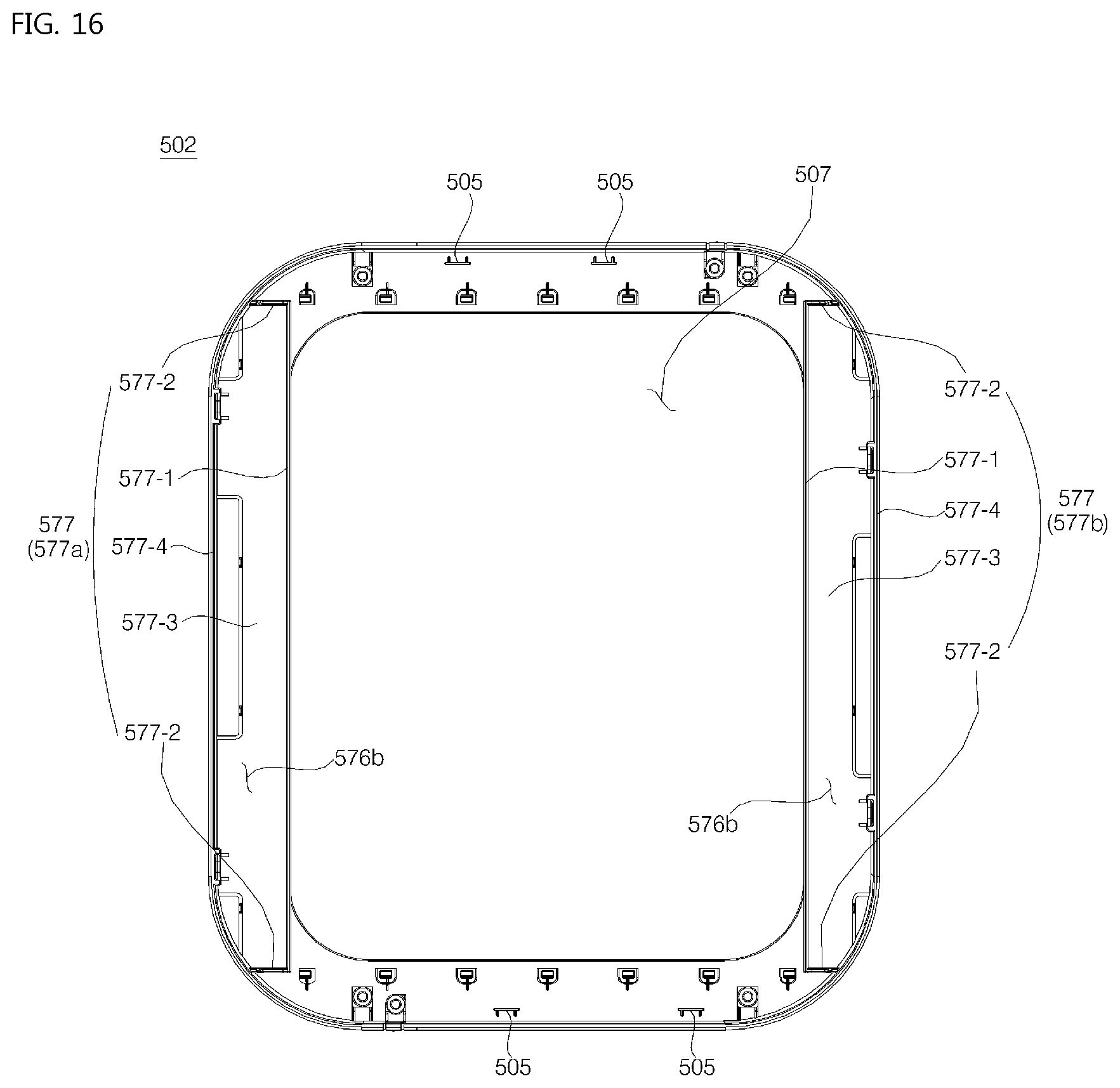
D00016

D00017

D00018

D00019

D00020

D00021

D00022

D00023

D00024

D00025

D00026

D00027

XML
uspto.report is an independent third-party trademark research tool that is not affiliated, endorsed, or sponsored by the United States Patent and Trademark Office (USPTO) or any other governmental organization. The information provided by uspto.report is based on publicly available data at the time of writing and is intended for informational purposes only.
While we strive to provide accurate and up-to-date information, we do not guarantee the accuracy, completeness, reliability, or suitability of the information displayed on this site. The use of this site is at your own risk. Any reliance you place on such information is therefore strictly at your own risk.
All official trademark data, including owner information, should be verified by visiting the official USPTO website at www.uspto.gov. This site is not intended to replace professional legal advice and should not be used as a substitute for consulting with a legal professional who is knowledgeable about trademark law.