Rotatable crown for an electronic device
Bushnell , et al. Fe
U.S. patent number 10,551,798 [Application Number 15/597,145] was granted by the patent office on 2020-02-04 for rotatable crown for an electronic device. This patent grant is currently assigned to APPLE INC.. The grantee listed for this patent is Apple Inc.. Invention is credited to Tyler S. Bushnell, Adam T. Clavelle, Colin M. Ely, Sriram Moorthy, Huan Peng, Stephen N. Sweet, Christopher M. Werner.


View All Diagrams
| United States Patent | 10,551,798 |
| Bushnell , et al. | February 4, 2020 |
Rotatable crown for an electronic device
Abstract
A compact crown for an electronic device such as an electronic watch, including a set of wipers capable of determining a rotation angle, rotation direction, or rotation speed, is disclosed. The set of wipers is in contact with at least one resistance member at different angular positions around a rotation axis. The crown may have a group of ground taps disposed along the resistance member and a measured signal may vary based on the position of each wiper as it contacts the at least one resistance member. A compact crown may also include capacitive members and capacitive sensors in order to similarly determine rotation angle, rotation direction, or rotation speed.
| Inventors: | Bushnell; Tyler S. (Mountain View, CA), Clavelle; Adam T. (Cupertino, CA), Werner; Christopher M. (San Jose, CA), Ely; Colin M. (Sunnyvale, CA), Sweet; Stephen N. (Cupertino, CA), Moorthy; Sriram (Cupertino, CA), Peng; Huan (Cupertino, CA) | ||||||||||
|---|---|---|---|---|---|---|---|---|---|---|---|
| Applicant: |
|
||||||||||
| Assignee: | APPLE INC. (Cupertino,
CA) |
||||||||||
| Family ID: | 69230068 | ||||||||||
| Appl. No.: | 15/597,145 | ||||||||||
| Filed: | May 16, 2017 |
Related U.S. Patent Documents
| Application Number | Filing Date | Patent Number | Issue Date | ||
|---|---|---|---|---|---|
| 62337804 | May 17, 2016 | ||||
| Current U.S. Class: | 1/1 |
| Current CPC Class: | G04C 3/008 (20130101); G04G 21/00 (20130101); G01D 5/1655 (20130101); G01D 5/2412 (20130101); G04C 3/002 (20130101); G04B 3/04 (20130101) |
| Current International Class: | G04G 21/00 (20100101); G01D 5/165 (20060101); G04B 3/04 (20060101) |
References Cited [Referenced By]
U.S. Patent Documents
| 2237860 | April 1941 | Bolle |
| 2288215 | June 1942 | Taubert et al. |
| 2497935 | February 1950 | Feurer |
| 2771734 | November 1956 | Morf |
| 2788236 | April 1957 | Kafowi |
| 2797592 | July 1957 | Marrapese |
| 3040514 | June 1962 | Dinstman |
| 3056030 | September 1962 | Kelchner |
| 3130539 | April 1964 | Davis |
| 3355873 | December 1967 | Morf |
| 3362154 | January 1968 | Perret |
| 3410247 | November 1968 | Dronberger |
| 3495398 | February 1970 | Widmer et al. |
| 3577876 | May 1971 | Spadini |
| 3621649 | November 1971 | Vulcan et al. |
| 3662618 | May 1972 | Kroll et al. |
| 3733803 | May 1973 | Hiraga |
| 4007347 | February 1977 | Haber |
| 4031341 | June 1977 | Wuthrich et al. |
| 4037068 | July 1977 | Gaynor |
| 4077200 | March 1978 | Schneider |
| 4133404 | January 1979 | Griffin |
| 4170104 | October 1979 | Yamagata |
| 4258096 | March 1981 | LaMarche |
| 4287400 | September 1981 | Kitik |
| 4289400 | September 1981 | Kubola et al. |
| 4311026 | January 1982 | Ochoa |
| 4311990 | January 1982 | Burke |
| 4324956 | April 1982 | Sakakino et al. |
| 4345119 | August 1982 | Latasiewicz |
| 4364674 | December 1982 | Tesch |
| 4379642 | April 1983 | Meyrat |
| 4395134 | July 1983 | Luce |
| 4396298 | August 1983 | Ripley |
| 4417824 | November 1983 | Paterson et al. |
| 4520306 | May 1985 | Kirby |
| 4581509 | April 1986 | Sanford et al. |
| 4600316 | July 1986 | Besson |
| 4617461 | October 1986 | Subbarao et al. |
| 4634861 | January 1987 | Ching et al. |
| 4641026 | February 1987 | Garcia, Jr. |
| 4670737 | June 1987 | Rilling |
| 4766642 | August 1988 | Gaffney et al. |
| 4783772 | November 1988 | Umemoto et al. |
| 4884073 | November 1989 | Souloumiac |
| 4914831 | April 1990 | Kanezashi et al. |
| 4922070 | May 1990 | Dorkinski |
| 4931794 | June 1990 | Haag |
| 4952799 | August 1990 | Loewen |
| 4980685 | December 1990 | Souloumiac et al. |
| 4987299 | January 1991 | Kobayashi et al. |
| 5034602 | July 1991 | Garcia et al. |
| 5214278 | May 1993 | Banda |
| 5258592 | November 1993 | Nishikawa et al. |
| 5288993 | February 1994 | Bidiville et al. |
| 5347123 | September 1994 | Jackson et al. |
| 5383166 | January 1995 | Gallay |
| 5471054 | November 1995 | Watanabe |
| 5509174 | April 1996 | Worrell |
| 5572314 | November 1996 | Hyman et al. |
| 5583560 | December 1996 | Florin et al. |
| 5631881 | May 1997 | Pessey et al. |
| 5726645 | March 1998 | Kamon et al. |
| 5748111 | May 1998 | Bates |
| 5825353 | October 1998 | Will |
| 5841050 | November 1998 | Clift et al. |
| 5847335 | December 1998 | Sugahara et al. |
| 5867082 | February 1999 | Van Zeeland |
| 5943233 | August 1999 | Ebina |
| 5953001 | September 1999 | Challener et al. |
| 5960366 | September 1999 | Duwaer et al. |
| 5963332 | October 1999 | Feldman et al. |
| 5999168 | December 1999 | Rosenberg et al. |
| 6069567 | May 2000 | Zawilski |
| 6134189 | October 2000 | Carrard |
| 6154201 | November 2000 | Levin et al. |
| 6175679 | January 2001 | Veligdan et al. |
| 6241684 | June 2001 | Amano |
| 6246050 | June 2001 | Tullis et al. |
| 6252825 | June 2001 | Perotto |
| 6304247 | October 2001 | Black |
| 6355891 | March 2002 | Ikunami |
| 6361502 | March 2002 | Puolakanaho et al. |
| 6377239 | April 2002 | Isikawa |
| 6392640 | May 2002 | Will |
| 6396006 | May 2002 | Yokoji et al. |
| 6422740 | July 2002 | Leuenberger |
| 6477117 | November 2002 | Narayanaswami et al. |
| 6502982 | January 2003 | Bach et al. |
| 6525278 | February 2003 | Villain et al. |
| 6556222 | April 2003 | Narayanaswami |
| 6575618 | June 2003 | Inoue et al. |
| 6587400 | July 2003 | Line |
| 6646635 | November 2003 | Pogatetz et al. |
| 6661438 | November 2003 | Billman |
| 6672758 | January 2004 | Ehrsam et al. |
| 6794992 | September 2004 | Rogers |
| 6809275 | October 2004 | Cheng et al. |
| 6834430 | December 2004 | Worrell |
| 6846998 | January 2005 | Hasumi et al. |
| 6882596 | April 2005 | Guanter |
| 6888076 | May 2005 | Hetherington |
| 6896403 | May 2005 | Gau |
| 6909378 | June 2005 | Lambrechts et al. |
| 6914551 | July 2005 | Vidal |
| 6961099 | November 2005 | Takano et al. |
| 6963039 | November 2005 | Weng et al. |
| 6967903 | November 2005 | Guanter |
| 6977868 | December 2005 | Brewer et al. |
| 6982930 | January 2006 | Hung |
| 6985107 | January 2006 | Anson |
| 6987568 | January 2006 | Dana |
| 6998553 | February 2006 | Hisamune et al. |
| 7016263 | March 2006 | Gueissaz et al. |
| 7021442 | April 2006 | Borgerson |
| 7034237 | April 2006 | Ferri et al. |
| 7081905 | July 2006 | Raghunath et al. |
| 7102626 | September 2006 | Denny, III |
| 7111365 | September 2006 | Howie, Jr. |
| 7113450 | September 2006 | Plancon et al. |
| 7119289 | October 2006 | Lacroix |
| 7135673 | November 2006 | Saint Clair |
| 7167083 | January 2007 | Giles |
| 7244927 | July 2007 | Huynh |
| 7255473 | August 2007 | Hiranuma et al. |
| 7265336 | September 2007 | Hataguchi et al. |
| 7274303 | September 2007 | Dresti et al. |
| 7285738 | October 2007 | Lavigne et al. |
| 7286063 | October 2007 | Gauthey |
| 7292741 | November 2007 | Ishiyama et al. |
| 7358481 | April 2008 | Yeoh et al. |
| 7369308 | May 2008 | Tsuruta et al. |
| 7371745 | May 2008 | Ebright et al. |
| 7385874 | June 2008 | Vuilleumier |
| 7404667 | July 2008 | Born et al. |
| 7465917 | December 2008 | Chin et al. |
| 7468036 | December 2008 | Rulkov et al. |
| 7506269 | March 2009 | Lang et al. |
| 7520664 | April 2009 | Wai |
| 7528824 | May 2009 | Kong |
| 7545367 | June 2009 | Sunda et al. |
| 7591582 | September 2009 | Hiranuma et al. |
| 7593755 | September 2009 | Colando et al. |
| 7605846 | October 2009 | Watanabe |
| 7634263 | December 2009 | Louch et al. |
| 7646677 | January 2010 | Nakamura |
| 7655874 | February 2010 | Akieda |
| 7682070 | March 2010 | Burton |
| 7708457 | May 2010 | Girardin |
| 7710456 | May 2010 | Koshiba et al. |
| 7732724 | June 2010 | Otani et al. |
| 7761246 | July 2010 | Matsui |
| 7763819 | July 2010 | Ieda et al. |
| 7772507 | August 2010 | Orr |
| 7778115 | August 2010 | Ruchonnet |
| 7781726 | August 2010 | Matsui et al. |
| RE41637 | September 2010 | O'Hara et al. |
| 7791588 | September 2010 | Tierling et al. |
| 7791597 | September 2010 | Silverstein et al. |
| 7822469 | October 2010 | Lo |
| 7856255 | December 2010 | Tsuchiya et al. |
| 7858583 | December 2010 | Schmidt et al. |
| 7865324 | January 2011 | Lindberg |
| 7894957 | February 2011 | Carlson |
| 7946758 | May 2011 | Mooring |
| 8063892 | November 2011 | Shahoian et al. |
| 8138488 | March 2012 | Grot |
| 8143981 | March 2012 | Washizu et al. |
| 8167126 | May 2012 | Stiehl |
| 8169402 | May 2012 | Shahoian et al. |
| 8188989 | May 2012 | Levin et al. |
| 8195313 | June 2012 | Fadell et al. |
| 8229535 | July 2012 | Mensinger et al. |
| 8248815 | August 2012 | Yang et al. |
| 8263886 | September 2012 | Lin et al. |
| 8263889 | September 2012 | Takahashi et al. |
| 8294670 | October 2012 | Griffin et al. |
| 8312495 | November 2012 | Vanderhoff |
| 8368677 | February 2013 | Yamamoto |
| 8371745 | February 2013 | Manni |
| 8373661 | February 2013 | Lan et al. |
| 8410971 | April 2013 | Friedlander |
| 8432368 | April 2013 | Momeyer et al. |
| 8439559 | May 2013 | Luk et al. |
| 8441450 | May 2013 | Degner et al. |
| 8446713 | May 2013 | Lai |
| 8456430 | June 2013 | Oliver et al. |
| 8477118 | July 2013 | Lan et al. |
| 8493190 | July 2013 | Periquet et al. |
| 8508511 | August 2013 | Tanaka et al. |
| 8525777 | September 2013 | Stavely et al. |
| 8562489 | October 2013 | Burton et al. |
| 8568313 | October 2013 | Sadhu |
| 8576044 | November 2013 | Chapman |
| 8593598 | November 2013 | Chen et al. |
| 8607662 | December 2013 | Huang |
| 8614881 | December 2013 | Yoo |
| 8783944 | February 2014 | Doi |
| 8666682 | March 2014 | LaVigne et al. |
| 8677285 | March 2014 | Tsern et al. |
| 8704787 | April 2014 | Yamamoto |
| 8711093 | April 2014 | Ong et al. |
| 8724087 | May 2014 | Van De Kerkhof et al. |
| 8730167 | May 2014 | Ming et al. |
| 8743088 | June 2014 | Watanabe |
| 8804993 | August 2014 | Shukla et al. |
| 8816962 | August 2014 | Obermeyer et al. |
| 8824245 | September 2014 | Lau et al. |
| 8847741 | September 2014 | Birnbaum et al. |
| 8859971 | October 2014 | Weber |
| 8860674 | October 2014 | Lee et al. |
| 8863219 | October 2014 | Brown et al. |
| D717679 | November 2014 | Anderssen |
| 8878657 | November 2014 | Periquet et al. |
| 8885856 | November 2014 | Sacha |
| 8895911 | November 2014 | Takahashi |
| 8905631 | December 2014 | Sakurazawa et al. |
| 8908477 | December 2014 | Peters |
| 8920022 | December 2014 | Ishida et al. |
| 8922399 | December 2014 | Bajaj et al. |
| 8928452 | January 2015 | Kim et al. |
| 8954135 | February 2015 | Yuen et al. |
| 8975543 | March 2015 | Hakemeyer |
| 8994827 | March 2015 | Mistry et al. |
| 9001625 | April 2015 | Essery et al. |
| 9024733 | May 2015 | Wouters |
| 9028134 | May 2015 | Koshoji et al. |
| 9030446 | May 2015 | Mistry et al. |
| 9034666 | May 2015 | Vaganov et al. |
| 9039614 | May 2015 | Yuen et al. |
| 9041663 | May 2015 | Westerman |
| 9042971 | May 2015 | Brumback et al. |
| 9052696 | June 2015 | Breuillot et al. |
| 9086717 | July 2015 | Meerovitsch |
| 9086738 | July 2015 | Leung et al. |
| 9101184 | August 2015 | Wilson |
| 9105413 | August 2015 | Hiranuma et al. |
| 9123483 | September 2015 | Ferri et al. |
| 9141087 | September 2015 | Brown et al. |
| 9176577 | November 2015 | Jangaard et al. |
| 9176598 | November 2015 | Sweetser et al. |
| 9202372 | December 2015 | Reams et al. |
| 9213409 | December 2015 | Redelsheimer et al. |
| 9223296 | December 2015 | Yang et al. |
| 9241635 | January 2016 | Yuen et al. |
| 9244438 | January 2016 | Hoover et al. |
| 9256209 | February 2016 | Yang et al. |
| 9277156 | March 2016 | Bennett et al. |
| 9350850 | May 2016 | Pope et al. |
| 9386932 | July 2016 | Chatterjee et al. |
| 9426275 | August 2016 | Eim et al. |
| 9430042 | August 2016 | Levin |
| 9437357 | September 2016 | Furuki et al. |
| 9449770 | September 2016 | Sanford et al. |
| 9501044 | November 2016 | Jackson et al. |
| 9520100 | December 2016 | Houjou et al. |
| 9532723 | January 2017 | Kim |
| 9545541 | January 2017 | Aragones et al. |
| 9552023 | January 2017 | Joo et al. |
| 9599964 | March 2017 | Gracia |
| 9607505 | March 2017 | Rothkopf et al. |
| 9620312 | April 2017 | Ely et al. |
| 9627163 | April 2017 | Ely |
| 9632318 | April 2017 | Goto et al. |
| 9651922 | May 2017 | Hysek et al. |
| 9659482 | May 2017 | Yang et al. |
| 9680831 | June 2017 | Jooste et al. |
| 9709956 | July 2017 | Ely et al. |
| D800172 | October 2017 | Akana |
| 9800717 | October 2017 | Ma et al. |
| 9836025 | December 2017 | Ely et al. |
| 9898032 | February 2018 | Hafez et al. |
| 9939923 | April 2018 | Sharma |
| 9946297 | April 2018 | Nazzaro et al. |
| 9971305 | May 2018 | Ely et al. |
| 9971405 | May 2018 | Holenarsipur et al. |
| 9979426 | May 2018 | Na et al. |
| 10001817 | June 2018 | Zambetti et al. |
| 10092203 | October 2018 | Mirov |
| 10114342 | October 2018 | Kim et al. |
| 10209148 | February 2019 | Lyon et al. |
| 10331082 | June 2019 | Ely et al. |
| 2003/0174590 | September 2003 | Arikawa et al. |
| 2004/0047244 | March 2004 | Iino et al. |
| 2004/0082414 | April 2004 | Knox |
| 2004/0130971 | July 2004 | Ecoffet et al. |
| 2004/0264301 | December 2004 | Howard et al. |
| 2005/0075558 | April 2005 | Vecerina et al. |
| 2005/0088417 | April 2005 | Mulligan |
| 2006/0250377 | November 2006 | Zadesky et al. |
| 2007/0013775 | January 2007 | Shin |
| 2007/0050054 | March 2007 | Sambandam Guruparan et al. |
| 2007/0211042 | September 2007 | Kim et al. |
| 2007/0222756 | September 2007 | Wu et al. |
| 2007/0229671 | October 2007 | Takeshita et al. |
| 2007/0247421 | October 2007 | Orsley et al. |
| 2008/0130914 | June 2008 | Cho |
| 2009/0051649 | February 2009 | Rondel |
| 2009/0073119 | March 2009 | Le et al. |
| 2009/0122656 | May 2009 | Bonnet et al. |
| 2009/0146975 | June 2009 | Chang |
| 2009/0152452 | June 2009 | Lee et al. |
| 2009/0217207 | August 2009 | Kagermeier et al. |
| 2009/0285443 | November 2009 | Camp et al. |
| 2009/0312051 | December 2009 | Hansson et al. |
| 2010/0033430 | February 2010 | Kakutani et al. |
| 2010/0053468 | March 2010 | Havrill |
| 2010/0081375 | April 2010 | Rosenblatt et al. |
| 2010/0149099 | June 2010 | Elias |
| 2011/0007468 | January 2011 | Burton et al. |
| 2011/0090148 | April 2011 | Li et al. |
| 2011/0158057 | June 2011 | Brewer et al. |
| 2011/0211355 | September 2011 | Hakemeyer |
| 2011/0242064 | October 2011 | Ono et al. |
| 2011/0270358 | November 2011 | Davis et al. |
| 2012/0067711 | March 2012 | Yang |
| 2012/0068857 | March 2012 | Rothkopf et al. |
| 2012/0075082 | March 2012 | Rothkopf et al. |
| 2012/0112859 | May 2012 | Park et al. |
| 2012/0113044 | May 2012 | Strazisar et al. |
| 2012/0206248 | August 2012 | Biggs |
| 2012/0272784 | November 2012 | Bailey et al. |
| 2013/0037396 | February 2013 | Yu |
| 2013/0087443 | April 2013 | Kikuchi |
| 2013/0191220 | July 2013 | Dent et al. |
| 2013/0235704 | September 2013 | Grinberg |
| 2013/0261405 | October 2013 | Lee et al. |
| 2013/0335196 | December 2013 | Zhang et al. |
| 2014/0071050 | March 2014 | Armstrong-Muntner |
| 2014/0071098 | March 2014 | You |
| 2014/0073486 | March 2014 | Ahmed et al. |
| 2014/0132516 | May 2014 | Tsai et al. |
| 2014/0197936 | July 2014 | Biggs et al. |
| 2014/0327630 | November 2014 | Burr et al. |
| 2014/0340318 | November 2014 | Stringer et al. |
| 2014/0347289 | November 2014 | Suh et al. |
| 2014/0368442 | December 2014 | Vahtola |
| 2014/0375579 | December 2014 | Fujiwara |
| 2015/0049059 | February 2015 | Zadesky et al. |
| 2015/0098309 | April 2015 | Adams et al. |
| 2015/0124415 | May 2015 | Goyal et al. |
| 2015/0186609 | July 2015 | Utter, II |
| 2015/0221460 | August 2015 | Teplitxky et al. |
| 2015/0227217 | August 2015 | Fukumoto |
| 2015/0320346 | November 2015 | Chen |
| 2015/0338642 | November 2015 | Sanford |
| 2015/0341031 | November 2015 | Marquas et al. |
| 2015/0366098 | December 2015 | Lapetina et al. |
| 2016/0018846 | January 2016 | Zenoff |
| 2016/0054813 | February 2016 | Shediwy et al. |
| 2016/0058375 | March 2016 | Rothkopf et al. |
| 2016/0061636 | March 2016 | Gowreesunker et al. |
| 2016/0062623 | March 2016 | Howard et al. |
| 2016/0069713 | March 2016 | Ruh et al. |
| 2016/0098016 | April 2016 | Ely et al. |
| 2016/0103985 | April 2016 | Shim et al. |
| 2016/0109861 | April 2016 | Kim et al. |
| 2016/0116306 | April 2016 | Ferri et al. |
| 2016/0147432 | May 2016 | Shi et al. |
| 2016/0168178 | June 2016 | Misra |
| 2016/0170598 | June 2016 | Zambetti et al. |
| 2016/0170608 | June 2016 | Zambetti et al. |
| 2016/0170624 | June 2016 | Zambetti et al. |
| 2016/0241688 | August 2016 | Vossoughi |
| 2016/0253487 | September 2016 | Sarkar et al. |
| 2016/0258784 | September 2016 | Boonsom et al. |
| 2016/0259301 | September 2016 | Ely |
| 2016/0306437 | October 2016 | Zhang et al. |
| 2016/0306446 | October 2016 | Chung et al. |
| 2016/0313703 | October 2016 | Ely et al. |
| 2016/0320583 | November 2016 | Hall, Jr. |
| 2016/0327911 | November 2016 | Eim et al. |
| 2016/0338642 | November 2016 | Parara et al. |
| 2016/0378069 | December 2016 | Rothkopf et al. |
| 2016/0378070 | December 2016 | Rothkopf et al. |
| 2016/0378071 | December 2016 | Rothkopf et al. |
| 2016/0378072 | December 2016 | Ely et al. |
| 2017/0003655 | January 2017 | Ely |
| 2017/0010751 | January 2017 | Shedletsky |
| 2017/0011210 | January 2017 | Cheong et al. |
| 2017/0027461 | February 2017 | Shin et al. |
| 2017/0031449 | February 2017 | Karsten et al. |
| 2017/0045958 | February 2017 | Battlogg et al. |
| 2017/0061863 | March 2017 | Eguchi |
| 2017/0069443 | March 2017 | Wang et al. |
| 2017/0069444 | March 2017 | Wang et al. |
| 2017/0069447 | March 2017 | Wang et al. |
| 2017/0090599 | March 2017 | Kuboyama |
| 2017/0104902 | April 2017 | Kim et al. |
| 2017/0139489 | May 2017 | Chen et al. |
| 2017/0216519 | August 2017 | Vouillamoz |
| 2017/0216668 | August 2017 | Burton et al. |
| 2017/0238138 | August 2017 | Aminzade |
| 2017/0248986 | August 2017 | Jackson et al. |
| 2017/0251561 | August 2017 | Fleck et al. |
| 2017/0269715 | September 2017 | Kim et al. |
| 2017/0285404 | October 2017 | Kubota et al. |
| 2017/0301314 | October 2017 | Kim et al. |
| 2017/0307414 | October 2017 | Ferri et al. |
| 2017/0331869 | November 2017 | Bendahan et al. |
| 2017/0357465 | December 2017 | Dzeryn et al. |
| 2018/0018026 | January 2018 | Bushnell et al. |
| 2018/0024683 | January 2018 | Ely et al. |
| 2018/0136613 | May 2018 | Ely et al. |
| 2018/0136686 | May 2018 | Jackson et al. |
| 2018/0196517 | July 2018 | Tan et al. |
| 2018/0235491 | August 2018 | Bayley et al. |
| 2018/0239306 | August 2018 | Ely |
| 2018/0246469 | August 2018 | Ely et al. |
| 2018/0299834 | October 2018 | Ely et al. |
| 2018/0307363 | October 2018 | Ely et al. |
| 2018/0329368 | November 2018 | Ely et al. |
| 2018/0335891 | November 2018 | Shedletsky et al. |
| 2018/0341342 | November 2018 | Bushnell et al. |
| 2018/0364815 | December 2018 | Moussette et al. |
| 2019/0017846 | January 2019 | Boonsom et al. |
| 2019/0163324 | May 2019 | Shedletsky |
| 2019/0250754 | August 2019 | Ely et al. |
| 1888928 | Jan 1937 | CH | |||
| 1302740 | Sep 2001 | CN | |||
| 1445627 | Oct 2003 | CN | |||
| 1504843 | Jun 2004 | CN | |||
| 1624427 | Jun 2005 | CN | |||
| 1792295 | Jun 2006 | CN | |||
| 101201587 | Jun 2008 | CN | |||
| 201081979 | Jul 2008 | CN | |||
| 201262741 | Jun 2009 | CN | |||
| 101750958 | Jun 2010 | CN | |||
| 201638168 | Nov 2010 | CN | |||
| 101923314 | Dec 2010 | CN | |||
| 202008579 | Oct 2011 | CN | |||
| 102890443 | Jan 2013 | CN | |||
| 202710937 | Jan 2013 | CN | |||
| 103191557 | Jul 2013 | CN | |||
| 103253067 | Aug 2013 | CN | |||
| 103645804 | Mar 2014 | CN | |||
| 203564224 | Apr 2014 | CN | |||
| 103852090 | Jun 2014 | CN | |||
| 203630524 | Jun 2014 | CN | |||
| 103956006 | Jul 2014 | CN | |||
| 203693601 | Jul 2014 | CN | |||
| 203732900 | Jul 2014 | CN | |||
| 103995456 | Aug 2014 | CN | |||
| 203941395 | Nov 2014 | CN | |||
| 104777987 | Apr 2015 | CN | |||
| 104685794 | Jun 2015 | CN | |||
| 104880937 | Sep 2015 | CN | |||
| 204650147 | Sep 2015 | CN | |||
| 105096979 | Nov 2015 | CN | |||
| 105547146 | May 2016 | CN | |||
| 3706194 | Sep 1988 | DE | |||
| 102008023651 | Nov 2009 | DE | |||
| 102016215087 | Mar 2017 | DE | |||
| 0556155 | Aug 1993 | EP | |||
| 1345095 | Sep 2003 | EP | |||
| 1669724 | Jun 2006 | EP | |||
| 1832969 | Sep 2007 | EP | |||
| 2375295 | Oct 2011 | EP | |||
| 2720129 | Apr 2014 | EP | |||
| 2884239 | Jun 2015 | EP | |||
| 2030093 | Oct 1970 | FR | |||
| 2801402 | May 2001 | FR | |||
| 2433211 | Jun 2007 | GB | |||
| S52151058 | Dec 1977 | JP | |||
| S54087779 | Jun 1979 | JP | |||
| S5708582 | Jan 1982 | JP | |||
| S5734457 | Feb 1982 | JP | |||
| H02285214 | Nov 1990 | JP | |||
| H04093719 | Mar 1992 | JP | |||
| H04157319 | May 1992 | JP | |||
| H05203465 | Aug 1993 | JP | |||
| H05312595 | Nov 1993 | JP | |||
| H06050927 | Dec 1994 | JP | |||
| H06331761 | Dec 1994 | JP | |||
| H06347293 | Dec 1994 | JP | |||
| H10161811 | Jun 1998 | JP | |||
| 11121210 | Apr 1999 | JP | |||
| H11191508 | Jul 1999 | JP | |||
| 2000337892 | Dec 2000 | JP | |||
| 2001084934 | Mar 2001 | JP | |||
| 2001167651 | Jun 2001 | JP | |||
| 2001202178 | Jul 2001 | JP | |||
| 2003050668 | Feb 2003 | JP | |||
| 2003151410 | May 2003 | JP | |||
| 2003331693 | Nov 2003 | JP | |||
| 2004184396 | Jul 2004 | JP | |||
| 2005017011 | Jan 2005 | JP | |||
| 2005063200 | Mar 2005 | JP | |||
| 2005108630 | Apr 2005 | JP | |||
| 2006164275 | Jun 2006 | JP | |||
| 2007149620 | Jun 2007 | JP | |||
| 2007248176 | Sep 2007 | JP | |||
| 2007311153 | Nov 2007 | JP | |||
| 2008053980 | Mar 2008 | JP | |||
| 2008122124 | May 2008 | JP | |||
| 2008122377 | May 2008 | JP | |||
| 2008170436 | Jul 2008 | JP | |||
| 2008235226 | Oct 2008 | JP | |||
| 2009070657 | Apr 2009 | JP | |||
| 2010032545 | Feb 2010 | JP | |||
| 2010165001 | Jul 2010 | JP | |||
| 2010186572 | Aug 2010 | JP | |||
| 2010243344 | Oct 2010 | JP | |||
| 2010244797 | Oct 2010 | JP | |||
| 2011165468 | Aug 2011 | JP | |||
| 2013057516 | Mar 2013 | JP | |||
| 2013079961 | May 2013 | JP | |||
| 2014174031 | Sep 2014 | JP | |||
| 20010030477 | Apr 2001 | KR | |||
| 20070011685 | Jan 2007 | KR | |||
| 20070014247 | Feb 2007 | KR | |||
| 100754674 | Sep 2007 | KR | |||
| 20080045397 | May 2008 | KR | |||
| 2020100007563 | Jul 2010 | KR | |||
| 20110011393 | Feb 2011 | KR | |||
| 20110012784 | Feb 2011 | KR | |||
| 20110113368 | Oct 2011 | KR | |||
| 20160017070 | Feb 2016 | KR | |||
| 1040225 | Nov 2014 | NL | |||
| 129033 | Nov 2013 | RO | |||
| 200633681 | Oct 2006 | TW | |||
| WO2001/022038 | Mar 2001 | WO | |||
| WO2001/069567 | Sep 2001 | WO | |||
| WO2010/058376 | May 2010 | WO | |||
| WO2012/083380 | Jun 2012 | WO | |||
| WO2012/094805 | Jul 2012 | WO | |||
| WO2014/018118 | Jan 2014 | WO | |||
| WO2014/200766 | Dec 2014 | WO | |||
| WO2015/147756 | Oct 2015 | WO | |||
| WO2016/104922 | Jun 2016 | WO | |||
| WO2016/155761 | Oct 2016 | WO | |||
| WO2017/013278 | Jan 2017 | WO | |||
Other References
|
US. Appl. No. 16/134,888, filed Sep. 18, 2018, pending. cited by applicant . U.S. Appl. No. 16/179,870, filed Nov. 2, 2018, pending. cited by applicant . U.S. Appl. No. 16/179,872, filed Nov. 2, 2018, pending. cited by applicant . U.S. Appl. No. 16/191,349, filed Nov. 14, 2018, pending. cited by applicant . Author Unknown, "How Vesag Helps Kids Women and Visitors," http://www.sooperarticles.com/health-fitness-articles/children-health-art- icles/how-vesag-helps-kids-women-visitors-218542.html, 2 pages, at least as early as May 20, 2015. cited by applicant . Author Unknown, "mHealth," http://mhealth.vesag.com/?m=201012, 7 pages, Dec. 23, 2010. cited by applicant . Author Unknown, "mHealth Summit 2010," http://www.virtualpressoffice.com/eventsSubmenu.do?page=exhibitorPage&sho- wId=1551&companyId=5394, 5 pages, Nov. 18, 2010. cited by applicant . Author Unknown, "RedEye mini Plug-in Universal Remote Adapter for iPhone, iPod touch and iPad," Amazon.com, 4 pages, date unknown. cited by applicant . Author Unknown, "Re iPhone Universal Remote Control--Infrared Remote Control Accessory for iPhone and iPod touch," http://www.amazon.com/iPhone-Universal-Remote-Control-Accessory/dp/tech-d- ata/B0038Z4 . . . , 2 pages, at least as early as Jul. 15, 2010. cited by applicant . Author Unknown, "Vesag Wrist Watch for Dementia Care from Vyzin," http://vyasa-kaaranam-ketkadey.blogspot.com/2011/03/vesag-wrist-watch-for- -dementia-care.html, 2 pages, Mar. 31, 2011. cited by applicant . Author Unknown, "Vyzin Electronics Private Limited launches Vesag Watch," http://www.virtualpressoffice.com/showJointPage.do?page=jp&showId=1544, 5 pages, Jan. 6, 2011. cited by applicant . Author Unknown, "Vyzin Unveiled Personal Emergency Response System (PERS) with Remote Health Monitoring That Can Be Used for Entire Family," http://www.24-7pressrelease.com/press-release/vyzin-unveiled-personal-eme- rgency-response-system-pers-with-remote-health-monitoring-that-can-be-used- -for-entire-family-219317.php, 2 pages, Jun. 17, 2011. cited by applicant . Author Unknown, "DeskThorityNet, Optical Switch Keyboards," http://deskthority.net/keyboards-f2/optical-switch-keyboards-t1474.html, 22 pages, Jul. 11, 2015. cited by applicant . Epstein et al., "Economical, High-Performance Optical Encoders," Hewlett-Packard Journal, pp. 99-106, Oct. 1988. [text only version]. cited by applicant . GreyB, "Google Watch: Convert your arm into a keyboard," http://www.whatafuture.com/2014/02/28/google-smartwatch/#sthash.Yk35cDXK.- dpbs, 3 pages, Feb. 28, 2014. cited by applicant . IBM, "Additional Functionality Added to Cell Phone via "Learning" Function Button," www.ip.com, 2 pages, Feb. 21, 2007. cited by applicant . Kim, Joseph, "2010 mHealth Summit Emerges as Major One-Stop U.S. Venue for Mobile Health," http://www.medicineandtechnology.com/2010/08/2010-mhealth-summit-emerges-- as-major.html, 3 pages, Aug. 26, 2010. cited by applicant . Krishnan et al., "A Miniature Surface Mount Reflective Optical Shaft Encoder," Hewlett-Packard Journal, Article 8, pp. 1-6, Dec. 1996. cited by applicant . Rick, "How Vesag Helps Health Conscious Citizens," http://sensetekgroup.com/2010/11/29/wireless-health-monitoring-system/, 2 pages, Nov. 29, 2010. cited by applicant . Sadhu, Rajendra, "How Vesag Helps People Who Want to `Be There`?," http://ezinearticles.com/?How-Vesag-Helps-People-Who-Want-to-Be-There?&id- -5423873, 1 page, Nov. 22, 2010. cited by applicant . Sadhu, Rajendra, "Mobile Innovation Helps Dementia and Alzheimer's Patients," http://www.itnewsafrica.com/2010/11/mobile-innovation-helps-dementia-anda- lzheimer%E2%80%99s-patients/, 3 pages, Nov. 22, 2010. cited by applicant . Sherr, Sol, "Input Devices," p. 55, Mar. 1988. cited by applicant . Tran et al., "Universal Programmable Remote Control/Telephone," www.ip.com, 2 pages, May 1, 1992. cited by applicant . Author Unknown, "Desirable Android Wear smartwatch from LG," Gulf News, Dubai, 3 pages, Jan. 30, 2015. cited by applicant . Author Unknown, "Fossil Q ups smartwatch game with handsome design and build," Business Mirror, Makati City, Philippines, 3 pages, Dec. 20, 2016. cited by applicant . Author Unknown, "MyKronoz ZeTime: World's Most Funded Hybrid Smartwatch Raised over $3M on Kickstarter, Running until Apr. 27th," Business Wire, New York, New York, 3 pages, Apr. 21, 2017. cited by applicant. |
Primary Examiner: Kayes; Sean P
Attorney, Agent or Firm: Brownstein Hyatt Farber Schreck, LLP
Parent Case Text
CROSS-REFERENCE TO RELATED APPLICATION(S)
This application is a nonprovisional patent application of and claims the benefit of U.S. Provisional Patent Application No. 62/337,804, filed May 17, 2016 and titled "Compact Rotary Encoder," the disclosure of which is hereby incorporated herein by reference in its entirety.
Claims
What is claimed is:
1. An electronic watch, comprising: a housing; a crown at least partially positioned within the housing and configured to receive rotational and translational input, and comprising: a shaft; a resistance member; and a set of wipers affixed to the shaft and operative to travel along the resistance member during rotation of the shaft, the set of wipers providing an output based on multiple contact points between the set of wipers and the resistance member; a display positioned at least partially within the housing and configured to depict a graphic in response to at least one of the rotational input or the translational input; an analog-to-digital converter electrically connected to the set of wipers, the analog-to-digital converter configured to provide a digital output corresponding to the output; and a processor configured to determine an angular position, a direction of rotation, or a speed of rotation of the shaft using the digital output, and to manipulate the graphic in response to the determined angular position, the direction of rotation, or the speed of rotation; wherein each wiper divides a resistance of the resistance member at each contact point, and a voltage at each contact point of the multiple contact points varies in response to rotation of the shaft.
2. The electronic watch of claim 1, wherein: the resistance member is circular; the resistance member has a constant resistance along its circumference; and the set of wipers maintains constant contact with the resistance member.
3. The electronic watch of claim 1, wherein: the resistance member comprises a first segment and a second segment separated by a ground tap; the set of wipers comprises a first wiper and a second wiper; and during rotation of the shaft, the first wiper divides the first segment at a first contact point of the multiple contact points while the second wiper divides the second segment at a second contact point.
4. The electronic watch of claim 3, wherein a first resistance of the first segment is equal to a second resistance of the second segment.
5. The electronic watch of claim 3, wherein: the first segment has a constant resistance; and the first contact point defines, in the first segment, two portions having a cumulative resistance equal to the constant resistance of the first segment.
6. The electronic watch of claim 5, wherein a resistance of each of the two portions varies in response to rotation of the shaft while maintaining the cumulative resistance equal to the constant resistance of the first segment.
7. The electronic watch of claim 5, wherein the first wiper and the second wiper maintain electrical contact with the resistance member during rotation of the shaft.
8. The electronic watch of claim 1, wherein: the resistance member comprises a first resistive track and a second resistive track; the electronic watch further comprises a switch configured to electrically activate the first resistive track while electrically floating the second resistive track, and to electrically activate the second resistive track while electrically floating the first resistive track; the set of wipers comprises a first wiper that travels along the first resistive track and a second wiper that travels along the second resistive track; the first wiper is electrically connected to the second wiper; and the output comprises a first output associated with the first wiper and a second output associated with the second wiper.
9. The electronic watch of claim 1, wherein: the resistance member comprises a resistive track; the set of wipers comprises a first wiper that travels along the resistive track and a second wiper that travels along the resistive track; the first wiper is electrically isolated from the second wiper; and the output comprises a first output associated with the first wiper and a second output associated with the second wiper.
10. The electronic watch of claim 9, further comprising: a first conductive output track; a second conductive output track; a third wiper affixed to the shaft and electrically connected to the first wiper, and operative to travel along the first conductive output track during rotation of the shaft; and a fourth wiper affixed to the shaft and electrically connected to the second wiper, and operative to travel along the second conductive output track during rotation of the shaft.
11. The electronic watch of claim 1, wherein: the resistance member comprises a resistive track; the set of wipers comprises a first wiper that travels along the resistive track and a second wiper that travels along the resistive track; the first wiper is electrically connected to the second wiper; and the output comprises an output associated with both the first wiper and the second wiper.
12. The electronic watch of claim 11, further comprising: a voltage input; a resistor; a constant current regulation circuit; and a reference voltage output, wherein the resistive track is coupled between the reference voltage output and the constant current regulation circuit; and the voltage input is coupled to the reference voltage output via the resistor.
13. A crown for an electronic watch, comprising: a resistance member on a contact surface; a rotatable shaft; an array of ground taps separating the resistance member into segments of uniform resistivity; a first wiper and a second wiper affixed to the rotatable shaft, the first wiper configured to generate a first output based on a relative position of the first wiper with respect to the resistance member and the second wiper configured to generate a second output based on a relative position of the second wiper with respect to the resistance member; and a processor configured to determine at least one of an angular position, a direction of rotation, or a speed of rotation of the rotatable shaft based on the first output and the second output, wherein: the crown is configured to receive a rotational input and a translational input; and the first wiper and the second wiper are affixed to the rotatable shaft such that the first wiper contacts the resistance member at a first segment that is distinct from a second segment contacted by the second wiper.
14. The crown of claim 13, wherein: a display is configured to depict a graphic in response to at least one of the rotational or translational input; and the processor is configured to manipulate the graphic in response to the determined angular position, direction of rotation, or speed of rotation.
15. The crown of claim 13, wherein the array of ground taps is positioned on the resistance member such that the segments have a substantially similar size.
16. The crown of claim 13, wherein the resistance member comprises a first resistive track and a second resistive track, the crown further comprising: an array of voltage inputs connected to the resistance member, the array of voltage inputs including a voltage input positioned between each set of adjacent ground taps along the resistance member; and a switch connected to at least the array of voltage inputs and configured to electrically activate the first resistive track while electrically floating the second resistive track, and to electrically activate the second resistive track while electrically floating the first resistive track, wherein the first wiper is electrically connected to the second wiper.
17. The crown of claim 13, further comprising: a dome switch, wherein the rotatable shaft is translatable and has a first end configured to depress and activate the dome switch in response to translation of the rotatable shaft.
Description
FIELD
The described embodiments relate generally to compact crowns for electronic devices such as electronic watches. More particularly, the present embodiments relate to a crown having (or taking the form of) a high-resolution rotary encoder that detects a rotation angle or relative amount of motion using an output from two or more angularly offset wipers.
BACKGROUND
In computing systems, a rotary encoder may be employed to detect an angular position or motion of a shaft. Many traditional rotary encoders use optical sensing of indicia placed around a circumference of an encoder surface or wheel. The precision of such rotary encoders is therefore limited by the minimum achievable size and spacing of the indicia. Optical sensing of indicia may also limit the ability of a traditional rotary encoder to detect a direction of rotation of a rotatable shaft of the encoder.
SUMMARY
Embodiments of the present invention are directed to a crown for an electronic device, which crown may be configured to determine an angular position, direction of rotation, or speed of rotation of a user-rotatable shaft or other user-rotatable element, for example, to control a function of the electronic device. The controlled function may include, for example, a graphical output of a display on the electronic device or a volume of an audio output of the electronic device.
In a first aspect, the present disclosure describes an electronic watch. The electronic watch includes a housing; a crown at least partially positioned within the housing and configured to receive rotational and translational input from a user, and comprising: a shaft; a resistance member; and a set of wipers affixed to the shaft and operative to travel along the resistance member during rotation of the shaft, the set of wipers providing an output based on multiple contact points between the set of wipers and the resistance member; a display positioned at least partially within the housing and configured to depict a graphic in response to at least one of the rotational or translational input; an analog-to-digital converter electrically connected to the set of wipers, the analog-to-digital converter configured to provide a digital output corresponding to the output; and a processor configured to determine an angular position, direction of rotation, or speed of rotation of the shaft using the digital output, and to manipulate the graphic in response to the determined angular position, direction of rotation, or speed of rotation; wherein each wiper divides a resistance of the resistance member at each contact point, and a voltage at each contact point of the multiple contact points varies in response to rotation of the shaft.
Another aspect of the present disclosure may take the form of a method for controlling an electronic watch, comprising: receiving an output signal from a crown of the electronic watch; identifying, based on the output signal, a first angle of rotation of a first wiper of the crown about an axis of a shaft of the crown, the first wiper in contact with a resistive track or a conductive output track of the crown; identifying, based on the output signal, a second angle of rotation of a second wiper of the crown about an axis of the shaft of the crown, the second wiper in contact with the resistive track; and controlling a function of the electronic watch based on at least one of the first and second angles of rotation.
Still another aspect of the disclosure may take the form of a crown for an electronic watch, comprising: a resistance member on a contact surface; a user-rotatable shaft; an array of ground taps separating the resistance member into segments of uniform resistivity; a first wiper and a second wiper affixed to the user-rotatable shaft, the first wiper configured to generate a first output and the second wiper configured to generate a second output based on a relative position of the first wiper or the second wiper with respect to the resistance member; and a processor configured to determine at least one of an angular position, a direction of rotation, or a speed of rotation of the user-rotatable shaft based on the first output and the second output, wherein the first wiper and the second wiper are affixed to the user-rotatable shaft such that the first wiper contacts the resistance member at a first segment that is distinct from a second segment contacted by the second wiper.
In addition to the exemplary aspects and embodiments described above, further aspects and embodiments will become apparent by reference to the drawings and by study of the following description.
BRIEF DESCRIPTION OF THE DRAWINGS
The disclosure will be readily understood by the following detailed description in conjunction with the accompanying drawings, wherein like reference numerals designate like structural elements, and in which:
FIG. 1 shows a sample electronic device that may incorporate a rotary encoder in the form of a crown, as described herein;
FIG. 2 shows an electrical block diagram of the electronic device of FIG. 1;
FIG. 3 shows a sample rotary encoder according to one example embodiment;
FIG. 4 shows a simplified electrical diagram of the rotary encoder of FIG. 3;
FIGS. 5A-5B show sample circuit diagrams formed by the rotary encoder of FIG. 3;
FIGS. 6A-6B show sample voltage vs. position graphs of the rotary encoder of FIG. 3;
FIG. 7 shows a simplified electrical diagram of a rotary encoder according to another example;
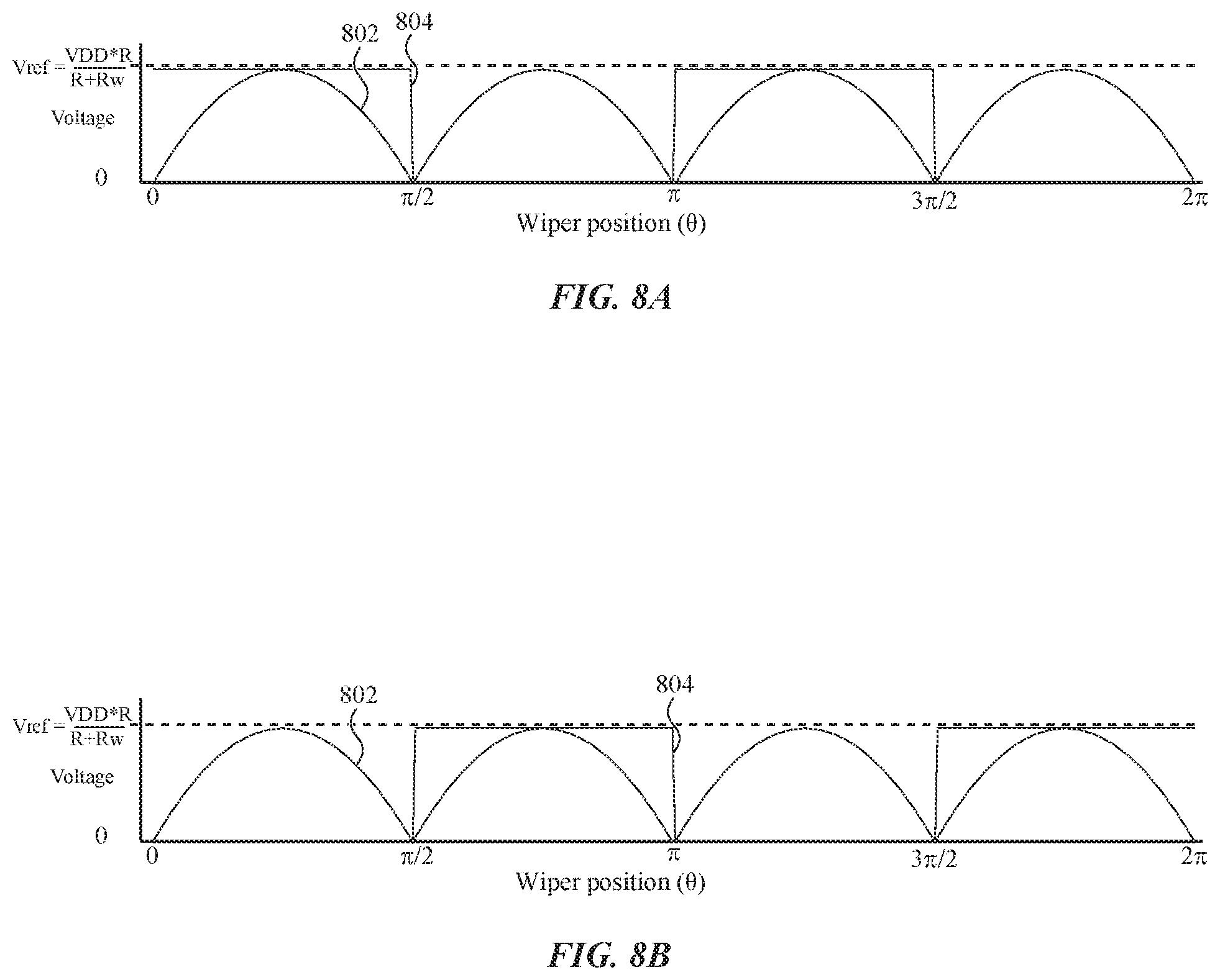
FIGS. 8A-8B show sample voltage vs. position graphs of the rotary encoder of FIG. 7;
FIGS. 9A-9B show a simplified electrical diagram of a rotary encoder according to another example;
FIG. 10 shows a sample circuit diagram formed by the rotary encoder of FIG. 9;
FIG. 11 shows a sample voltage vs. position graph of the rotary encoder of FIG. 9;
FIG. 12 shows a timing diagram for the rotary encoder of FIG. 9;
FIG. 13 shows a simplified electrical diagram of a rotary encoder according to another example;
FIG. 14 shows a sample circuit diagram formed by the rotary encoder of FIG. 13;
FIG. 15 shows a simplified electrical diagram of a rotary encoder according to another example;
FIG. 16 shows a sample circuit diagram formed by the rotary encoder of FIG. 15;
FIG. 17 shows a sample voltage vs. position graph of the rotary encoder of FIG. 15;
FIG. 18 shows another example of a rotary encoder;
FIG. 19 shows a top view of a portion of the rotary encoder of FIG. 18;
FIGS. 20A-20B show sample capacitance vs. position graphs of the rotary encoder of FIG. 18; and
FIG. 21 illustrates a method that may be performed to control a function of an electronic device based on an angle of rotation of a wiper of a rotary encoder about an axis of a rotatable element of the rotary encoder.
FIG. 22A illustrates a list, displayed on an electronic device, that may be controlled by rotation of a crown.
FIG. 22B illustrates the list of FIG. 22A, changed in response to rotation of the crown.
FIG. 23A illustrates an electronic device displaying a picture, the magnification of which may be controlled by rotation of a crown.
FIG. 23B illustrates the picture of FIG. 23A, changed in response to rotation of the crown.
FIG. 24A illustrates an electronic device displaying a question that may be answered by rotating a crown.
FIG. 24B illustrates the electronic device of FIG. 23A, with the question answered through rotation of the crown.
DETAILED DESCRIPTION
Reference will now be made in detail to representative embodiments illustrated in the accompanying drawings. It should be understood that the following descriptions are not intended to limit the embodiments to one preferred embodiment. To the contrary, it is intended to cover alternatives, modifications, and equivalents as can be included within the spirit and scope of the described embodiments as defined by the appended claims.
The following disclosure relates to a compact rotary encoder capable of high resolution output for use in an electronic device such as an electronic watch. More particularly, the rotary encoder may be used as, or connected to, a crown of an electronic watch. The crown may function as an input device of the electronic device, and may be selectively rotated about an axis. The relative rotation around the axis may be used to control a feature, interface, or other mechanism of the electronic device. The high resolution of the rotary encoder, functioning as a crown (or as part of a crown), may allow for precise control of an electronic device. In some examples, the rotary encoder may control or vary any or all of: a graphic shown on a display on the electronic device; a function of the electronic device; a haptic output of the electronic device; and/or a volume of an audio output of the electronic device.
In an embodiment, the crown (e.g., rotary encoder) may have a user-rotatable shaft, at least two arms extending radially from the shaft and separated by an angle, and a wiper or slider coupled to each arm. Each wiper may extend from the arm at an angle and contact at least one resistance member on a contact surface of a rotary encoder base. In some embodiments, the arms may extend at a non-right angle from the shaft. In some examples, the arms may be replaced by one or more rotors, or by a portion of the shaft that extends outward from an axis of the crown, which portion provides or supports the wipers, sliders, or other electrical contact members. The contact surface may also have a group of ground taps electrically coupled to the resistance member and at least one conductive element disposed radially around the shaft. In some embodiments, the resistance member may form a circle, track, path, or the like. Further, the resistance member may be divided into multiple segments.
As the shaft is rotated about its axis (e.g., by a user), each wiper contacts a different portion of the resistance member and experiences a variable resistance as a result of the wiper "dividing" a portion of the resistance member between ground points into at least two segments. That is, as the shaft rotates, the wiper varies the length of segments of the resistance member between the wiper contact point and grounded points disposed around the resistance member. The output signals for each wiper may be detected and monitored by a processor to determine a rotation angle (i.e., angle of rotation or angular position), rotation direction (i.e., direction of rotation), or rotation speed (i.e., speed of rotation) around the shaft axis.
In some embodiments, the at least two arms (or the at least two contact members that are otherwise affixed to the shaft) are separated by an angle. This may cause each respective wiper to contact the resistance member at points at which the output signals are out of phase. The particular angle of separation for the arms (or contact members) may be chosen such that the output signals from the wipers, when plotted as a function of the rotation angle, are signals in quadrature (e.g., signals separated by a predetermined offset). Accordingly, by determining the phase difference between signals from the respective wipers, a direction of rotation can be determined.
In another embodiment, the rotary encoder/crown may have a shaft and at least two capacitive members extending radially from the shaft and separated by an angle. The capacitive members may rotate above the base of the rotary encoder member. The base of the rotary encoder/crown may include a set of capacitance sensors positioned on a sensing surface beneath the shaft. The capacitance sensors may be coaxial with the shaft. The capacitive sensors may detect a capacitance between themselves and the capacitive members. As the shaft rotates, the capacitive members may pass over the capacitive sensors. Capacitance between a capacitive member and a capacitive sensor increases as overlap between the member and sensor increases, and decreases as overlap decreases. The capacitive member may revolve as the shaft rotates, thereby varying the overlap of the capacitive member with respect to the capacitive sensor. As the shaft rotates, this overlap may vary from zero to full, or anywhere in between.
The capacitive members and the group of capacitance sensors may be configured to maintain a constant separation during rotation of the capacitive members around the shaft axis. The output signals of the capacitance sensors may be detected and monitored by a processor to determine a rotation angle, rotation direction, or rotation speed of the shaft around the shaft axis.
These and other embodiments are discussed below with reference to FIGS. 1-21. However, those skilled in the art will readily appreciate that the detailed description given herein with respect to these Figures is for explanatory purposes only and should not be construed as limiting.
Turning now to the figures, FIG. 1 illustrates an electronic device 100 such as a wearable electronic device, timekeeping device, portable computing device, mobile phone, touch-sensitive input, or the like. The electronic device 100 may have a housing 102 defining a body, a display 104 configured to depict a graphical output of the electronic device 100, and at least one input device or selection device 106. An input device 106 may be positioned at least partially within the housing 102 and may project through the housing so that a user may manipulate the input device (for example, by rotating it). Likewise, the display 104 may be positioned at least partially within the housing 102 and may be accessible by, and visible to, a user. The user may view information presented on the display and may touch the display to provide a touch or force input. As one example, the user may select (or otherwise interact with) a graphic, icon, or the like presented on the display by touching or pressing on the display at the location of the graphic.
The electronic device 100 may have a band 108 for securing the electronic device 100 to a user, another electronic device, a retaining mechanism, and so on. In some embodiments, the electronic device 100 may be an electronic watch, the body defined by the housing 102 may be a watch body, and the input device 106 may be a crown of the electronic watch. The crown may extend from an exterior to an interior of the electronic device housing. The crown may be configured to receive rotational and translational input from a user. The input device 106 may include a scroll wheel, knob, dial, or the like that may be operated by a user of the electronic device 100. Some embodiments of the electronic device 100 may lack the band 108, display 104, or both.
The electronic device 100 may include a number of internal components. FIG. 2 illustrates a simplified block diagram 200 of the electronic device 100. The electronic device 100 may include, by way of non-limiting example, one or more processors 202, a storage or memory 204, an input/output interface 206, a display 210, a power source 212, and one or more sensors 208, each of which will be discussed in turn below.
The processor 202 may control operation of the electronic device 100. The processor 202 may be in communication, either directly or indirectly, with substantially all of the components of the electronic device 100. For example, one or more system buses 201 or other communication mechanisms may provide communication between the processor 202, the display 210, the input/output interface 206, the sensors 208, and so on. The processor 202 may be any electronic device capable of processing, receiving, and/or transmitting instructions. For example, the processor 202 may be a microprocessor or a microcomputer. As described herein, the term "processor" is meant to encompass a single processor or processing unit, multiple processors, or multiple processing units, or other suitably configured computing element(s).
In some examples, the function(s) of the electronic device 100 controlled by the processor 202 may include a graphical output of a display 210 on the electronic device 100. For example, in response to detecting rotation of the input device 106 (e.g., a changed angular position, direction of rotation, or speed of rotation of a rotary encoder, which rotary encoder may be a crown or part of a crown), the processor 202 may change or manipulate (e.g., scroll, zoom, pan, move, etc.) a graphic depicted on the display 210. Scrolling may be within a graphic (e.g., a photo or map), within text and/or images of a document or web page (which are specific examples of graphics), within an array of graphics representing applications or functions that may be selected, launched, and so on. The processor 202 may cause graphics on a display to scroll in a particular direction based on a determined direction of rotation of the input device 106, or may cause scrolling at a speed based on a determined speed of rotation of the input device 106. FIGS. 22A-24B, discussed below, provide examples of how a rotatable input device 106, such as a crown, may be used to interact with an electronic device and manipulate or change graphics on an associated display.
As another example, rotating the input device 106 may cause different graphics, icons, information, or the like to be shown on the display so that a user may select or otherwise interact with such graphics/icons/information (collectively, a "graphic"). The user may interact with a graphic by touching or applying force to a portion of the display 104 depicting the graphic, through rotational input to the input device 106, through translational input to the input device 106 (e.g., pressing a crown toward the housing of the electronic device), and so on.
The processor 202 may also or alternatively adjust a volume of an audio output of the electronic device 100 in response to detecting rotation of the input device 106. The volume may be adjusted up or down based on a direction of rotation of the input device 106. The processor 202 may also or alternatively adjust other settings of the electronic device 100 (or settings of applications hosted on or accessed by the electronic device 100) in response to detecting rotation of the input device 106 (e.g., the processor 202 may adjust the time displayed by a clock function of the electronic device 100). In some examples, the processor 202 may control movement of a character or item within a game based on a detected rotation (change in angular position), direction of rotation, or speed of rotation of the input device 106.
In some examples, the function of the electronic device 100 controlled by the processor 202 may be determined based on a context of the electronic device 100 or processor 202. For example, the processor 202 may adjust a volume of an audio output of the electronic device 100 when the input device 106 is rotated while an audio player is open or active on the electronic device 100, or the processor 202 may scroll through graphics representing applications or functions when the input device 106 is rotated while a home screen is displayed on the electronic device 100.
The memory 204 may store electronic data that may be utilized by the electronic device 100. For example, the memory 204 may store electrical data or content (e.g., audio files, video files, document files, and so on), corresponding to various applications. The memory 204 may be, for example, non-volatile storage, a magnetic storage medium, optical storage medium, magneto-optical storage medium, read only memory, random access memory, erasable programmable memory, or flash memory.
The input/output interface 206 may receive data from a user or one or more other electronic devices. Additionally, the input/output interface 206 may facilitate transmission of data to a user or to other electronic devices. For example, in embodiments where the electronic device 100 is an electronic watch, the input/output interface 206 may be used to receive data from a network, other electronic devices, or may be used to send and transmit electronic signals via a wireless or wired connection (Internet, Wi-Fi, Bluetooth, and Ethernet being a few examples). In some embodiments, the input/output interface 206 may support multiple network or communication mechanisms. For example, the input/output interface 206 may pair with another device over a Bluetooth network to transfer signals to the other device, while simultaneously receiving data from a Wi-Fi or other network. The input/output interface 206 may receive input signals from the sensors 208 and the processor 202 may control the input/output interface 206 to output control signals for the electronic device 100.
The power source 212 may be substantially any device capable of providing energy to the electronic device 100. For example, the power source 212 may be a battery, a connection cable that may be configured to connect the electronic device 100 to another power source such as a wall outlet, or the like.
The sensors 208 may include substantially any type of sensor. For example, the electronic device 100 may include one or more audio sensors (e.g., microphones), light sensors (e.g., ambient light sensors), gyroscopes, accelerometers, or the like. The sensors 208 may be used to provide data to the processor 202, which may be used to enhance or vary functions of the electronic device 100. In some embodiments, at least one of the sensors 208 may be a rotary encoder associated with the input device 106 of the electronic device 100 (e.g., a rotary encoder used as, or connected to, a crown of an electronic watch). In some embodiments, at least one of the sensors 208 may be a dome switch that may be depressed and activated by user translation of a crown of an electronic watch.
FIG. 3 illustrates an embodiment of a compact rotary encoder 300 for use in an electronic device, such as electronic device 100. In some embodiments, the rotary encoder 300 may function as the input device 106 of the electronic device 100 such that a shaft 306 of the rotary encoder 300 rotates when the input device 106 rotates. As one example, the input device (and thus the shaft and wipers) may rotate about a long axis of the shaft 306. Such rotation changes the shaft's angular position. As discussed above, in some embodiments, the input device 106 may be the rotating crown of an electronic watch. Similarly, any user-rotatable element may be used in place of a shaft. As previously mentioned, the rotary encoder 300, and other rotary encoders discussed herein, may be a crown of an electronic watch, or part of a crown of an electronic watch. Accordingly, discussions herein of rotary encoders should be understood to include crowns (or bezels, or other rotatable elements) of an electronic device, such as a watch, phone, tablet computing device, input mechanism, and so on.
The rotary encoder 300 may include a base 302, cover 304, and a contact surface 303 on the base 302. The cover 304 may include an aperture 308 through which a rotating shaft 306 passes, extending into an interior of the rotary encoder 300 (or associated device). It should be appreciated that the rotary encoder 300 may take the form of a crown, button, scroll wheel, or the like for an electronic device, and the cover 304 may be a housing of the electronic device. A user may manipulate a portion of the rotary encoder to cause the shaft 306 to rotate about an axis extending along a length of the shaft, in order to provide an input to the electronic device.
In some examples, the shaft 306 may be translatable and slide within the aperture 308, such that a terminal end or portion of the shaft is configured to depress or otherwise activate a dome switch 322 within the base 302. Although a dome switch is illustrated, other types of switches may be employed and actuated by translation of the shaft. At least two arms 310a, 310b may extend outwardly in a radial direction from the shaft 306. As discussed in more detail with respect to FIG. 4, the arms 310a, 310b may be coupled to the shaft 306 and separated by a radial angle. It will be appreciated that although two arms 310a, 310b are illustrated, more arms may be coupled to the shaft 306 (or other rotatable element) and separated by other angles. This may improve the resolution or accuracy of the angular position of the shaft detected by the rotary encoder 300.
Each arm 310a, 310b may include a contact member (e.g., a wiper or slider 312a, 312b, respectively). The wipers 312a, 312b may extend from the arms 310a, 310b at an angle such that the wipers 312a, 312b extend toward, and touch, the contact surface 303 of the base 302. Each wiper 312a, 312b may have a known resistance and may electrically couple the arms 310a, 310b to the contact surface 303 of the rotary encoder 300. Each wiper 312a, 312b contacts the contact surface 303 at a unique wiper contact point. In some examples, the arms 310a, 310b may be provided by one or more rotors, or the arms 310a, 310b may be replaced by a portion (or portions) of the shaft 306 that extends outward from the axis of the rotary encoder 300, and the contact members may be formed on or attached to a surface of the shaft 306 that faces the contact surface 303. It should be appreciated that the contact members/wipers need not be attached to an arm in any embodiment described herein, but instead may be attached to the shaft or to another structure that ultimately is affixed to the shaft.
The contact surface 303 of the base 302 may have a resistance member 314, such as a resistance pad, track, path, or the like provided thereon. In some embodiments, the resistance member 314 may be embedded into or integral with the contact surface 303, while in other embodiments the resistance member 314 may be adjacent, or deposited or otherwise formed on the contact surface 303. As shown in FIG. 3, the resistance member 314 may be disposed in a ring, circle, or other radial pattern around the rotation axis of the shaft 306. The resistance member 314 may have a uniform resistivity along its path, circumference, length, or other dimension. The electrical resistance of the resistance member 314 may be determined by dimensions of the member, such as its thickness, length, width, density, or other dimension. In some examples, the resistance member 314 may have constant concentrations of material such as gold, copper, silver, or other metals (including alloys), resistive polymers, ceramics, other suitable material, or a combination thereof to maintain a uniform resistivity. As will be discussed below, the uniform resistivity may be used to determine a position of a wiper 312a, 312b around the resistance member 314. A constant current source (such as a current regulation circuit) may supply current to the resistance member 314 in certain embodiments. The current source may provide a relatively fixed or invariant current, and thus may be considered a constant current source.
The contact surface 303 of the rotary encoder 300 may also include a conductive element 316 and a group of ground taps 318a-d. The conductive element 316 may be in constant electrical contact with the wipers 312a, 312b as they travel along the resistance member 314. In some embodiments, the conductive element 316 may be embedded or integral with the resistance member 314, while in other embodiments the conductive element 316 may be positioned above or below the resistance member 314.
The conductive element 316 facilitates the detection of an electrical signal provided to the wipers 312a, 312b, as discussed further below with respect to FIGS. 4 and 5. The wipers 312a, 312b may be shaped and angled to maintain electrical contact with the resistance member 314 and the conductive element 316 throughout rotation of the shaft 306. As illustrated in FIG. 3, the conductive element 316 may be shaped substantially the same as the resistance member 314 (e.g., in the shape of a circle or ring coaxially aligned with the axis of rotation of the shaft 306). As the shaft rotates, the angular positions of the shaft and the wipers change, and thus the wipers travel along the resistance member.
As illustrated in FIG. 3, the four ground taps 318a-d may be provided at equally spaced locations around the resistance member 314. However, the number of ground taps 318 may vary based on the number of wipers 312, the angle between wipers 312, a desired accuracy of the rotary encoder 300, the number of bits of an analog-to-digital converter (as discussed below), and the like. In some embodiments, the ground taps may be unequally spaced apart from one another.
The rotary encoder 300 may also include a group of electrical contacts 320a-d. The group of electrical contacts 320a-d may be included in the base 302 or top 304 and may be electrically coupled to the wipers 312, ground taps 318, conductive element 316, and resistance member 314. Electrical contacts 320a-d may provide input and output control of elements of the rotary encoder 300. In some embodiments at least one of the electrical contacts 320a-d may provide an output signal from wiper 312a, an output signal from wiper 312b, a control signal, a common ground, and the like.
With reference to FIG. 4, a simplified electrical diagram 400 illustrates the electrical connectivity of the rotary encoder 300. As shown in FIG. 4, a resistance member 402 is positioned coaxially around a shaft 410. A group of ground taps 404a-d, which may correspond to the ground taps 318a-d, may be provided around the resistance member 402. The total resistance of the resistance member 402 may be R and the resistance member 402 may have uniform resistivity as discussed above (e.g., uniform resistance per unit of material forming the resistance member 402). That is, when the resistance member 402 has a uniform resistivity, the total or cumulative resistance may be defined as R in the segment from .THETA.=0 to .THETA.=2.pi.. Accordingly, each quadrant Q1-Q4 may have a predefined resistance R.sub.Q1-R.sub.Q4, where R.sub.Q1+R.sub.Q2+R.sub.Q3+R.sub.Q4=R.
As the wiper travels along (e.g., rotates around) and maintains contact with the resistance member 402 in various locations, the wiper contact points 407, 409 form a voltage dividing circuit as discussed below. However, although a resistance member 402 having uniform resistivity has been discussed, it should be noted that the resistance member 402 may vary its resistance in a known or predetermined manner as a function of angular displacement around the shaft axis.
Although four ground taps 404 are illustrated in FIG. 4, it should be appreciated that more or fewer ground taps may be provided. The resolution of the rotary encoder 300 may vary based on the number n of ground taps provided. As shown in FIG. 4, the first wiper 406 (e.g., a first contact member) and second wiper 408 (e.g., a second contact member) may be separated by an angle .alpha.. This angle .alpha. may ensure that the first and second wipers 406, 408 output signals in quadrature. Output signals that are in quadrature are ones whose phases are offset by a preset amount or predetermined offset. In some embodiments, the angle .alpha. may depend on the number of ground taps. In a particular embodiment, the angle .alpha. may be determined by the formula .alpha.=.pi.(1/2n), where n is the number of ground taps 404.
As illustrated in the example of FIG. 4, a first wiper 406 may contact the resistance member 402 at a contact point 407 between .THETA.=0 and .THETA.=.pi./2 (e.g., quadrant Q1) around the resistance member 402. Put another way, the contact point 407 may define a first portion and a second portion of the resistance member 402. Accordingly, when a signal is applied such as a voltage VDD to the first wiper 406, a signal may be measured at the contact point; this measured voltage varies between VDD and zero volts (e.g., ground). In some embodiments, the voltage at the wiper contact point may be measured by including a conductive trace on the wiper itself (not shown). In other embodiments, the signal transmitted through the wiper(s) may be read out using a conductive element 316 on or embedded in the contact surface 303 of the base 302 of the rotary encoder 300 (see FIG. 3). The foregoing generally applies no matter which quadrant or at what contact point the wiper contacts the resistance member.
Generally, the voltage at the wiper contact point 407 is a function of the position of the first wiper 406 as measured along the resistance member 402. The wiper's contact point 407 is between two ground taps, unless it is at a ground tap. For example and as shown in FIG. 4, the contact point 407 is in quadrant Q1 of the resistance member 402, defined as the segment of the resistance member between a first ground tap 404a and a second ground tap 404b. The quadrant Q1 may be thought of as two separate portions or resistors; namely one resistor R1 extending from the first ground tap 404a to the wiper contact point 407, and a second resistor R2 extending from the first ground tap 404a to the wiper contact point. Each portion R1, R2 will have its own voltage, which will vary with the length of the portion (e.g., the distance from the contact point to an adjacent ground tap).
The second wiper 408 may contact the resistance member 402 at a contact point 407 between the ground tap 404b and 404c. A third resistance R3 may be formed between the contact point of the second wiper 408 and the ground tap 404b. A fourth resistance R4 may be formed between the contact point of the second wiper 408 and the ground tap 404c. As will be discussed below with respect to FIGS. 5A-5B, a circuit may be formed enabling readout of the electrical signal at the contact points of the respective wipers 406, 408.
Similarly, the voltage at the wiper contact point 409 is a function of the position of the wiper 408 as taken along the resistance member 402. The wiper's contact point 409 is between two ground taps, unless it is at a ground tap. For example and as shown in FIG. 4, the contact point 409 is in quadrant Q3 of the resistance member 402, defined as the portion of the resistance member 402 between a third ground tap 404c and a fourth ground tap 404d. The quadrant Q3 may be thought of as two separate portions or resistors; namely one resistor R3 extending from the third ground tap 404c to the wiper contact point 409, and a second resistor R4 extending from the fourth ground tap 404d to the wiper contact point 409.
It should be noted that the foregoing is but one example of contact point locations; the wipers may contact the resistive track at any points in any quadrants (or any segment between two ground taps, if the resistive track is not separated into quadrants). Accordingly, any portion of the resistive track between two ground points (e.g., any segment) may be modeled as two resistors that have resistances varying with distance between the contact point and ground tap.
The circuit shown in FIG. 5A represents the first wiper 406 contacting the resistance member 402. As shown in FIG. 5A, an input signal VDD may be provided to the first wiper; the first wiper has a wiper resistance Rw. In some embodiments, the first wiper may be the first wiper 406 of FIG. 4. At the contact point 407 between the first wiper and the resistance member 402, the input signal VDD is voltage divided by the first resistance R1 and the second resistance R2, as shown in FIG. 5A and similarly in FIG. 4. That is, the voltage at contact point 407 varies with the resistance Rw of the wiper, R1, and R2. As the wiper 406 is rotated to angle .THETA. around the shaft 410 axis (e.g., as the angular position of the shaft changes), the first and second resistances R1, R2 vary.
An input of an m-bit analog-to-digital Converter (ADC) may be electrically coupled to the contact point of the first wiper 406 while its output is electrically connected to a processor 202. The ADC may have a reference voltage Vref determined by the ratio of Rw to R, which is the total resistance of the resistance member 402 as discussed above. In one particular embodiment, the reference voltage Vref may be determined by the formula Vref=(VDD*R)/(R+Rw).
The m-bit ADC may output a digitized signal Wd1 of the voltage measured at the contact point of the first wiper 406 and the resistance member 402. The signal at the wiper contact point 407 may be detected and monitored over time by a processor 202, in order to determine a rotation position of the first wiper 406 and thus an angular position of the shaft, as discussed below with reference to FIG. 6.
Similar to FIG. 5A, above, FIG. 5B is an example circuit which represents when the second wiper 408 contacting the resistance member 402 at contact point 409 (see also FIG. 4). As shown in FIG. 5B, an input signal VDD may be provided to a second wiper having a wiper resistance Rw. In some embodiments, the second wiper may be the second wiper 408 as shown in FIG. 4.
At the contact point between the second wiper 408 and the resistance member 402, the input signal VDD is voltage divided by the third resistance R3 and the fourth resistance R4, as shown in FIG. 5B and similarly in FIG. 4. That is, the voltage at contact point 409 varies with the resistance Rw of the second wiper, R3, and R4. As the second wiper 408 is rotated at an angle .THETA. around the shaft 410 axis (e.g., as the angular position of the shaft changes), the third and fourth resistances R3, R4 vary.
An input of an m-bit Analog-to-Digital Converter (ADC) may be electrically coupled to the contact point of the second wiper 408 and may provide a digital output to a processor 202. The ADC may have a reference voltage Vref determined by the ratio of Rw to R (e.g., the total resistance of the resistance member 402). In one particular embodiment, the reference voltage Vref may be determined by the formula Vref=(VDD*R)/(R+Rw). Accordingly, for a given setup with a resistance member 402 having a total resistance R around its length, and given a wiper with a resistance of Rw, the value of Vref may be constant.
With continuing reference to FIG. 5B, the m-bit ADC may output a digitized signal Wd2 of the voltage measured at the contact point of the second wiper 408 and the resistance member 402. The signal at the wiper contact point 409 may be detected and monitored over time by a processor 202, in order to determine a rotation position of the first wiper 406 and thus an angular position of the shaft.
Turning now to FIGS. 6A and 6B, the outputs at wiper contact points 407 and 409 (as discussed above in FIG. 5) are plotted as voltages cycling between zero and a maximum voltage Vref. The figure illustrates the wiper contact voltages as functions of wiper angle .THETA., which is the angle between a wiper's current contact point and a zero-angle point on the resistance member (e.g., where .THETA.=0). Plot 602 may be a plot of the signal at the wiper contact point 407 of the first wiper 406, and line 604 may be a plot of the signal at the wiper contact point 409 of the second wiper 408. As shown in FIG. 6A, as the shaft 410 is rotated (e.g., its angular position changes) causing rotation of the first and second wipers 406, 408, the wiper contact point signals vary between zero and Vref. The plots 602 and 604 are out of phase by a constant, predetermined offset and thus considered to be in quadrature. The amount of quadrature or predetermined offset may depend on the angle .alpha. between the first and second wipers 406, 408. By determining a phase difference between plots 602 and 604, the rotational direction around the shaft 410 can be determined, as can the shaft's angular position. Such determination may be done by any suitable processor 202.
FIG. 6A depicts plot 602 as leading plot 604 (i.e., positively out of phase). Accordingly, FIG. 6A may be a plot reflecting rotation of the shaft 410 in a first direction (e.g., clockwise in FIG. 4). Similarly, FIG. 6B depicts plot 602 as lagging plot 604 (i.e., negatively out of phase). Thus, FIG. 6B may be a plot reflecting rotation of the shaft 410 in a second direction (e.g., counter-clockwise in FIG. 4).
Based on the above configuration, the resolution of the rotary encoder 300 may be adjusted to meet various design requirements. The resolution of the rotary encoder 300 may be approximately n*(2{circumflex over ( )}m), where n is the number of ground taps 404 and m is the number of bits in the m-bit ADC. Therefore, in order to increase resolution, one may provide more ground taps or a higher-bit ADC. Furthermore, one may choose an ADC and vary the number of ground taps n to increase or decrease resolution. Conversely, one may choose a number of ground taps n and vary the number of bits m of the ADC to increase or decrease resolution. The ADC may be connected electrically to, and provide digital output to, a processor 202, such that the digital output of the ADC may be used by the processor 202 to determine an angular position of the shaft.
With reference now to FIG. 7, a simplified electrical diagram 700 of another embodiment of a rotary encoder 300 is shown, as is also suitable for use in, or as, a crown of an electronic device. FIG. 7 illustrates the electrical connectivity of a rotary encoder similar to the rotary encoder 300 in FIG. 3 but with a single arm (e.g., a rotor) having a first and second contact member 706, 708 provided thereon. The first contact member 706 may be offset by an angle .alpha. from the second contact member 708. Here, .alpha.=.pi..
A resistive track 702 may be positioned coaxially around a shaft 710 (or other user-rotatable element). The first contact member 706 may contact the resistive track 702 at a first contact point 707. A group of electrical sinks 704a, 704b (which act as the ground taps previously described) may be provided around the resistive track 702. The total resistance of the resistive track 702 may be R, and the resistive track may have uniform resistivity as discussed above (e.g., a uniform resistance per unit volume of material forming the resistive track). A second resistive track 703 may be positioned radially inward from the first resistive track 702 and disposed in a half-circle around the shaft 710. The second contact member 708 may contact the second resistive track 703 at a second contact point 709. The radius of the second resistive track 703, which in this example is a half-circle, may be less than the radius of the circular resistive track 702. Another group of electrical sinks 704c, d may be spaced around the second resistive track 703. In one embodiment, second resistive track 703 may have one electrical sink 704c at one end and another electrical sink 704d at the other end.
As illustrated in FIG. 7, the first contact member 706 may contact the resistive track 702 at a first contact point 707 located somewhere between .THETA.=0 and .THETA.=.pi.. Accordingly, when a signal is applied (such as a voltage Vref) to the first contact member 706, an output voltage at the contact point may vary between Vref and zero volts (i.e., ground).
A third resistance R3 may be established between the contact point of the second contact member 708 and the electrical sink 704c. Similarly, a fourth resistance R4 may be established between the contact point of the second contact member 708 and the electrical sink 704d. As was discussed above with respect to FIGS. 5A-5B, a circuit may be formed enabling readout of the electrical signals at the contact points of the respective contact members 706, 708.
Generally, the voltage at the first contact member's 706 contact point 707 is a function of the position of the contact member 706 along the resistive track 702. The contact member's contact point 707 is between two electrical sinks, unless it is at an electrical sink. For example and as shown in FIG. 7, the contact point 707 is in quadrant Q1-Q2 of the resistive track 702, defined as the portion of the resistive track between a first electrical sink 704a and second electrical sink 704b. The quadrant Q1-Q2 may be thought of as two separate resistors, namely one resistor R1 extending from the first electrical sink 704a to the contact point 707, and a second resistor R2 extending from the second electrical sink 704b to the contact point 707.
Likewise, the voltage at the second contact member's 708 contact point 709 is a function of the position of the second contact member 708 along the second resistive track 703. The contact member's contact point 709 is between two ground taps, unless it is at a ground tap. For example and as shown in FIG. 7, the contact point 709 is in quadrant Q2-Q3 of the resistive track 703, defined as the portion of the resistance member between a third electrical sink 704c and a fourth electrical sink 704d. The quadrant Q2-Q3 may be thought of as two separate resistors, namely a third resistor R3 extending from the third electrical sink 704c to the contact point 709, and a fourth resistor R4 extending from the fourth electrical sink 704d to the wiper contact point 709.
Although four electrical sinks 704 are illustrated in FIG. 7, it should be appreciated that more or fewer electrical sinks may be provided. The resolution of the rotary encoder 300 may vary based on the number n of electrical sinks provided. As shown in FIG. 7, the first contact member 706 and the second contact member 708 may be offset from one another by an angle .alpha.=.pi..
The embodiment of FIG. 7 may have substantially the same circuitry as discussed above with respect to FIG. 5. That is, a voltage divider circuit is set up based on the contact position of the first contact member 706 on the first resistive track 702 and a second voltage divider circuit is formed based on the contact position of the second contact member 708 on the second resistive track 703. As the first contact member 706 is rotated around the shaft 710 axis, the first and second resistances R1, R2 vary. An input of an m-bit Analog-to-Digital Converter (ADC) may be electrically coupled to the contact point of the first contact member 706. The m-bit ADC may output a digitized signal Wd1 that is the voltage measured at the contact point between the first contact member 706 and the first resistive track 702. The signal at this contact point 707 may be detected and monitored over time in order to determine a rotational position of the first contact member 706 and thus an angular position of the shaft, as discussed below with reference to FIG. 8.
Similarly, as the second contact member 708 is rotated around the shaft 710 axis, the third and fourth resistances R3, R4 vary. An input of an m-bit Analog-to-Digital Converter (ADC) may be electrically coupled to the contact point of the second contact member 708. The m-bit ADC may output a digitized signal Wd2 of the voltage measured at this contact point between the second contact member 708 and the second resistive track 703. The digital signal Wd2 may be detected and monitored over time in order to determine a rotational position of the second contact member 708 and thus an angular position of the shaft, as discussed below with reference to FIGS. 8A-8B.
Turning now to FIGS. 8A-8B, the outputs at the contact points 707 and 709 are plotted as voltages cycling between zero and Vref as a function of contact member position around the axis of the shaft (e.g., the contact points and the angle .THETA. vary as the shaft revolves and a contact member travels along its resistive track). Plot 802 is a plot of the voltage of the first contact member 706 as measured at its contact point 707, and plot 804 is a plot of the voltage of the second contact member 708 as measured at its contact point 709.
With respect to FIG. 8A, rotating the shaft 710 (or other user-rotatable element) causes rotation of the first and second contact members 706, 708 and changes the shaft's angular position. As the contact members rotate around the shaft (e.g., the angle .THETA. changes), their output signals vary between zero and Vref. The output of the first contact member is shown as plot 802 and the output of the second contact member is shown as plot 804.
Due to the layout of the resistive tracks 702, 703 around the shaft 710, plots 802 and 804 may peak at Vref at different angles of rotation .THETA.. This information may be used to determine the rotational direction of the contact members 706, 708 around the shaft 710. For example, FIG. 8A may depict a rotation of the shaft 410 in a first direction (e.g., clockwise in FIG. 7). Similarly, FIG. 8B may depict a rotation of the shaft 710 in a second direction (e.g., counter-clockwise in FIG. 7).
With reference now to FIGS. 9A-9B, a simplified electrical diagram 900 of another embodiment of a rotary encoder is shown. As with the other rotary encoders discussed herein, the embodiment shown in FIGS. 9A-9B may be used as, or in, a crown of an electronic device (such as an electronic watch). FIG. 9A illustrates the electrical connectivity of a rotary encoder similar to the rotary encoder in FIG. 7 but with a conductive output track 902 and a somewhat different arrangement of resistive tracks 904, 906. The resistive tracks 904, 906 and conductive output track 902 may be circular, concentric, and positioned coaxially around a shaft 908. The resistive tracks 904, 906 and conductive output track 902 may be supported by a contact surface of a base of the rotary encoder.
The first resistive track 904 (e.g., a resistance member) may be positioned coaxially around the shaft 908 (or other rotatable element). A first contact member 910 (e.g., a first wiper) may contact the first resistive track 904 at a first contact point 912 and travel along the first resistive track 904 as the shaft 908 rotates with respect to an axis of the rotary encoder. A first array of electrical sinks 914a, 914b, 914c, 914d (which act as the ground taps previously described) may be provided around the first resistive track 904. The total resistance of the first resistive track 904 may be R1, and the first resistive track 904 may have uniform resistivity as discussed above (e.g., a uniform resistance per unit volume of material forming the resistive track). A second resistive track 906 may be positioned radially inward from the first resistive track 904 and disposed around the shaft 908. The total resistance of the second resistive track 906 may be R2, and the second resistive track 906 may have uniform resistivity as discussed above (e.g., a uniform resistance per unit volume of material forming the resistive track). R1 and R2 may be equal or unequal. A second contact member 916 (a second wiper) may contact the second resistive track 906 at a second contact point 918 and travel along the second resistive track 906 as the shaft 908 rotates with respect to the axis of the rotary encoder. The radius of the second resistive track 906 may be less than the radius of the first resistive track 904. A second array of electrical sinks 914e, 914f, 914g, 914h may be spaced around the second resistive track 906. In one embodiment, the electrical sinks 914a-h may be equally spaced about each of the first resistive track 904 and the second resistive track 906. The electrical sinks 914a-h are indicated by diamonds in FIG. 9A, while voltage inputs 920a-h (discussed below) are indicated by triangles. The shape is arbitrary and intended only to provide visual differentiation between the two.
The electrical sinks 914a-h may divide the first resistive track 904 and the second resistive track 906 into multiple segments. An array of voltage inputs may include a first array of voltage inputs 920a, 920b, 920c, 920d connected to the first resistive track 904 and a second array of voltage inputs 920e, 920f, 920g, 920h connected to the second resistive track 906. Each voltage input 920a-h may be positioned between a set of adjacent electrical sinks (e.g., voltage input 920a may be positioned between electrical sinks 914a and 914b, voltage input 920b may be positioned between electrical sinks 914b and 914c, etc.).
The conductive output track 902 may be positioned radially inward from the second resistive track 906 and disposed around the shaft 908. The radius of the conductive output track 902 may be less than the radius of the second resistive track 906. The conductive output track 902 may be electrically connected to a voltage output 922 via a conductor 924 (e.g., a conductive trace, wire, etc.). In alternative embodiments, the concentric relationships of the tracks may differ (e.g., the resistive tracks 904, 906 may be interior to the conductive output track 902).
The first and second contact members 910, 916 may be electrically connected and coupled (affixed) to the shaft 908. In some examples, the first and second contact members 910, 916 may be coupled to a single arm 926 (e.g., a rotor) that is affixed to and rotates with the shaft 908. The entirety of the arm 926 may be conductive, or the arm 926 may include conductive traces or wires that electrically connect the first and second contact members 910, 916. The first contact member 910 may be offset by an angle .alpha. (about the shaft 908) from the second contact member 916. Here, .alpha.=.pi.. A third contact member 928 (i.e., a third wiper) may be electrically connected to the first and second contact members 910, 916 and coupled to an arm 928 (which arm 928 may be configured similarly to the arm 926, replaced by a portion of the shaft 908 that extends over the resistive tracks 904, 906, etc.). The third contact member 928 may contact the conductive output track 902 at a third contact point 930. The third contact member 928 may travel along, contact, or wipe the conductive output track 902 as the shaft 908 rotates with respect to the conductive output track 902.
During rotation of the shaft 908 with respect to the axis of the rotary encoder, the angles of rotation (.THETA.) associated with the first contact member 910 and the second contact member 916 change with rotation of the shaft 908, and thus the angles of rotation (or locations) of the first contact point 912 and the second contact point 918 change with respect to an axis of the rotary encoder.
As shown in FIG. 9B, the rotary encoder may further include one or more switches 932 configured to electrically activate the first resistive track 904 while electrically floating the second resistive track 906, and to electrically activate the second resistive track 906 while electrically floating the first resistive track 904. For purposes of this description, a resistive track is electrically active when a current is intentionally induced to flow through the resistive track. As shown, the one or more switches 932 may include a first multiplexer 934 and a second multiplexer 936. The first multiplexer 934 may have an input 938 configured to receive a voltage (e.g., Vdd), a first output 940 to which the voltage may be applied (as Vdd_A) when the first multiplexer 934 is placed in a first state (e.g., a logic "0" state), and a second output 942 to which the voltage may be applied (as Vdd_B) when the first multiplexer 934 is placed in a second state (e.g., a logic "1" state). The first output 940 may be coupled to the first array of voltage inputs 920a-d and the second output 942 may be coupled to the second array of voltage inputs 920e-h. The second multiplexer 936 may have an input 944 configured to be coupled to ground, a first output 946 to which the ground may be connected (as Gnd_A) when the second multiplexer 936 is placed in a first state (e.g., a logic "0" state), and a second output 948 to which the ground may be connected (as Gnd_B) when the second multiplexer 936 is placed in a second state (e.g., a logic "1" state). The first output 946 may be coupled to the first array of electrical sinks 914a-d, and the second output 948 may be coupled to the second array of electrical sinks 914-e-h. In some examples, the control inputs of the first multiplexer 934 and the second multiplexer 936 may be electrically connected at a node 950 to which a common control signal (e.g., a binary control signal, CTRL) may be applied. The common control signal may alternately place each multiplexer 934, 936 in the logic "0" state or the logic "1" state.
When the first resistive track 904 is electrically active, and as rotation of the shaft 908 with respect to the axis of the rotary encoder causes the location of the first contact point 912 to change with respect to the first resistive track 904, the voltage at the first contact point 912 changes (i.e., the voltage is a variable voltage). Similarly, when the second resistive track 906 is electrically active, and as rotation of the shaft 908 with respect to the axis of the rotary encoder causes the location of the second contact point 918 to change with respect to the second resistive track 906, the voltage at the second contact point 918 changes (i.e., the voltage is a variable voltage). Because just one of the resistive tracks 904, 906 is electrically active at a time (while the other resistive track is floating), the voltages at the first contact point 912 and the second contact point 918 may be alternately output on the conductive output track 902. Despite the variance in the voltages at the first contact point 912 and the second contact point 918, the first resistive track 904, second resistive track 904, and/or other components of the rotary encoder may be configured to maintain a predetermined offset between the voltages.
Based on the voltages outputted on the conductive output track 902 (or at output 922), and the predetermined offset between the voltages, a processor may determine an angle of rotation of the first contact member 910, the second contact member 916, or the shaft 908. The processor may also or alternatively determine a direction of rotation or speed of rotation of the shaft 908.
The circuit shown in FIG. 10 represents the first contact member 910 contacting the first resistive track 904 and the second contact member 916 contacting the second resistive track 906. Each of the first and second resistive tracks is modeled as a set of resistors separated by grounds, in accordance with the diagram of FIG. 9A. As shown in FIG. 10, the first resistive track 904 may be electrically activated by coupling Vdd_A to the first array of voltage inputs 920a-d and coupling Gnd_A to the first array of electrical sinks 914a-d. Alternatively, the second resistive track 906 may be electrically activated by coupling Vdd_B to the second array of voltage inputs 920e-h and coupling Gnd_B to the second array of electrical sinks 914e-h. The voltages at the first and second contact points 912, 918 may be alternately output at the voltage output 922 (as Vout) via the first contact member 910, arm 926, and conductive output track 902 (see FIG. 9A), and via the second contact member 916, arm 926, and conductive output track 902. Each of the first contact member 910, second contact member 916, arm 926, and conductive output track 902 may be associated with an impedance and consequent voltage drop that affects the voltage obtained from the first or second contact point 912, 918.
Turning now to FIG. 11, an example of the voltages at the first contact point 912 and second contact point 918 (as discussed above in FIGS. 9A, 9B, and 10) are plotted as voltages cycling between zero and a maximum voltage Vref (e.g., Vdd_A or Vdd_B). The figure illustrates the voltages as a function of a rotation angle .THETA., which is the angle between a contact point and a zero-angle point of the resistive tracks 904, 906 (e.g., where .THETA.=0). Plot 1102 may be a plot of the voltage at the first contact point 912, and plot 1104 may be a plot of the voltage at the second contact point 918. As shown in FIG. 11, as the shaft 908 of the rotary encoder shown in FIG. 9A is rotated (e.g., as its angle of rotation or angular position changes), causing rotation of the first and second contact members 910, 916, the voltages vary between zero and Vref. Plots 1102 and 1104 are out of phase by a constant, predetermined offset, and are thus considered to be in quadrature. The amount of quadrature or predetermined offset may depend on the angle .alpha. between the first and second contact members 910, 916. By determining a phase difference between plots 1102 and 1104, the direction of rotation of the shaft 908 can be determined, as can the shaft's angular position. Such determinations may be made by any suitable processor 202.
FIG. 12 shows an example of a timing diagram for the rotary encoder shown in FIGS. 9A and 9B. As shown, the first resistive track 904 may be electrically activated during a first time period 1202 by connecting the first array of voltage inputs 920a-d to Vdd_A and the first array of electrical sinks 914a-d to Gnd_A. The second resistive track 906 may be electrically isolated (held at a high impedance state, z) during the first time period 1202. Similarly, the second resistive track 906 may be electrically activated during a second time period 1204 by connecting the second array of voltage inputs 920e-h to Vdd_A and the second array of electrical sinks 914e-h to Gnd_A. The first resistive track 904 may be electrically isolated (held at a high impedance state, z) during the second time period 1204. One or more switches, such as the first multiplexer 934 and the second multiplexer 936, may be operated to provide alternating instances of the first time period 1202 and the second time period 1204. In some examples, electrical activation of the first resistive track 904 or the second resistive track 906 may require assertion of an enable (EN) signal 1206. During each of the first time period 1202 and the second time period 1204, an ADC may obtain one or more samples 1208, 1210 of the voltage at the first contact point 912 or the second contact point 918. Obtaining multiple samples during each of the first time period 1202 and the second time period 1204 may improve direction of rotation or speed of rotation determinations.
With reference now to FIG. 13, a simplified electrical diagram 1300 of another embodiment of a rotary encoder is shown. FIG. 13 illustrates the electrical connectivity of a rotary encoder similar to the rotary encoder in FIGS. 9A-9B, but with a single resistive track 1302 and multiple conductive output tracks 1304, 1306. The resistive track 1302 and conductive output tracks 1304, 1306 may be circular, concentric, and positioned coaxially around a shaft 1308. The resistive track 1302 and conductive output tracks 1304, 1306 may be supported by a contact surface of a base of the rotary encoder.
The resistive track 1302 (i.e., a resistance member) may be positioned coaxially around the shaft 1308 (or other rotatable element). A first contact member 1310 (i.e., a first wiper) may contact the resistive track 1302 at a first contact point 1312 and travel along the resistive track 1302 as the shaft 1308 rotates with respect to an axis of the rotary encoder. A second contact member 1314 (i.e., a second wiper) may contact the resistive track 1302 at a second contact point 1316 and travel along (e.g., wipe) the resistive track 1302 as the shaft 1308 rotates with respect to the axis of the rotary encoder. The first contact member 1310 may be electrically connected to a first arm 1318 (e.g., a first rotor) that is affixed to and rotates with the shaft 1308. The second contact member 1314 may be electrically connected to a second arm 1320 (e.g., a second rotor) that is affixed to and rotates with the shaft 1308. The first arm 1318 may be electrically isolated from the second arm 1320. The entireties of the first and second arms 1318, 1320 may be conductive, or the first and second arms 1318, 1320 may include conductive traces or wires that electrically connect to the first or second contact member 1310, 1314. In other examples, the first and second contact members 1310, 1314 may be affixed to the shaft 1308 in other ways (e.g., the shaft 1308 may have a portion that extends outward from the axis of the rotary encoder and over the resistive track 1302, and the first and second contact members 1310, 1314 may be formed on or attached to a surface of the shaft 1308 that faces the resistive track 1302). The first contact member 1310 may be offset by an angle .alpha. (about the shaft 1308) from the second contact member 1310.
An array of electrical sinks 1322a, 1322b, 1322c, 1322d (which act as the ground taps previously described) may be provided around the resistive track 1302. The total resistance of the resistive track 1302 may be R, and the resistive track 1302 may have uniform resistivity as discussed above (e.g., a uniform resistance per unit volume of material forming the resistive track). In one embodiment, the electrical sinks 1322a-d may be equally spaced about the resistive track 1302. The electrical sinks 1322a-d may divide the resistive track 1302 into multiple segments. An array of voltage inputs 1324a, 1324b, 1324c, 1324d may also be connected to the resistive track 1302. Each voltage input 1324a-d may be positioned between a set of adjacent electrical sinks (e.g., voltage input 1324a may be positioned between electrical sinks 1322a and 1322b, voltage input 1324b may be positioned between electrical sinks 1322b and 1322c, etc.).
A first conductive output track 1304 and a second conductive output track 1306 may be positioned radially inward from the resistive track 1302 and disposed around the shaft 1308. The radius of the first conductive output track 1304 may be less than the radius of the resistive track 1302, and the radius of the second conductive output track 1306 may be less than the radius of the first conductive output track 1304. The first conductive output track 1304 may be electrically connected to a first voltage output 1326 via a first conductor 1328 (e.g., a conductive trace, wire, etc.), and the second conductive output track 1306 may be electrically connected to a second voltage output 1330 via a second conductor 1332. In alternative embodiments, the concentric relationships of the tracks may differ (e.g., the resistive track 1302 may be interior to the conductive output tracks 1304, 1306).
A third contact member 1334 (e.g., a third wiper) may be electrically connected to the first contact member 1310 and coupled to the first arm 1318 (or otherwise affixed to the shaft 1308). The third contact member 1334 may contact the first conductive output track 1304 at a third contact point 1336. The third contact member 1334 may contact, travel along, or otherwise wipe the conductive output track 1304 as the shaft 1308 rotates with respect to the axis of the rotary encoder. A fourth contact member 1338 (e.g., a fourth wiper) may be electrically connected to the second contact member 1314 and coupled to the second arm 1324 (or otherwise affixed to the shaft 1308). The fourth contact member 1338 may contact the second conductive output track 1306 at a fourth contact point 1340. The fourth contact member 1338 may contact or wipe the second conductive output track 1306 as the shaft 1308 rotates with respect to the axis of the rotary encoder.
During rotation of the shaft 1308 with respect to the axis of the rotary encoder, the angles of rotation (.THETA.) associated with the first contact member 1310 and the second contact member 1314 change with rotation of the shaft 1308, and thus the angles of rotation (or locations) of the first contact point 1312 and the second contact point 1316 change with respect to the axis of the rotary encoder.
As rotation of the shaft 1308 with respect to the axis of the rotary encoder causes the locations of the first and second contact points 1312, 1316 to change with respect to the resistive track 1302, the voltages at the first and second contact points 1312, 1316 change (e.g., the voltages are variable voltages). The voltage at the first contact point 1312 may be output via the first conductive output track 1304, and the voltage at the second contact point 1316 may be output via the second conductive output track 1306. Despite the variance in the voltages at the first contact point 1312 and the second contact point 1316, the resistive track 1302 and/or other components of the rotary encoder may be configured to maintain a predetermined offset between the voltages.
Based on the voltages (Vout0, Vout1) outputted on the first and second conductive output tracks 1304, 1306 (or at outputs 1326 and 1330), and the predetermined offset between the voltages, a processor may determine an angle of rotation of the first contact member 1310, the second contact member 1310, or the shaft 1308. The processor may also or alternatively determine a direction of rotation or speed of rotation of the shaft 1308.
The circuit shown in FIG. 14 represents the first and second contact members 1310, 1314 contacting the resistive track 1302. As shown in FIG. 14, the resistive track 1302 may be electrically activated by coupling Vdd to the array of voltage inputs 1324a-d and coupling Gnd to the array of electrical sinks 1322a-d. The voltages at the first and second contact points 1312, 1316 may be simultaneously output at the first and second voltage outputs 1326, 1330, as Vout_0 and Vout_1, via the first contact member 1310, first arm 1318, and first conductive output track 1304 (see FIG. 13), and via the second contact member 1314, second arm 1320, and second conductive output track 1306. Each of the first contact member 1310, second contact member 1314, first arm 1318, second arm 1320, firs
References
-
sooperarticles.com/health-fitness-articles/children-health-articles/how-vesag-helps-kids-women-visitors-218542.html
-
mhealth.vesag.com/?m=201012
-
virtualpressoffice.com/eventsSubmenu.do?page=exhibitorPage&showId=1551&companyId=5394
-
amazon.com/iPhone-Universal-Remote-Control-Accessory/dp/tech-data/B0038Z4
-
vyasa-kaaranam-ketkadey.blogspot.com/2011/03/vesag-wrist-watch-for-dementia-care.html
-
-
24-7pressrelease.com/press-release/vyzin-unveiled-personal-emergency-response-system-pers-with-remote-health-monitoring-that-can-be-used-for-entire-family-219317.php
-
deskthority.net/keyboards-f2/optical-switch-keyboards-t1474.html
-
whatafuture.com/2014/02/28/google-smartwatch/#sthash.Yk35cDXK.dpbs
-
ip.com
-
medicineandtechnology.com/2010/08/2010-mhealth-summit-emerges-as-major.html
-
sensetekgroup.com/2010/11/29/wireless-health-monitoring-system
-
ezinearticles.com/?How-Vesag-Helps-People-Who-Want-to-Be-There?&id-5423873
-
itnewsafrica.com/2010/11/mobile-innovation-helps-dementia-andalzheimer%E2%80%99s-patients
D00000
D00001
D00002
D00003
D00004
D00005
D00006
D00007
D00008
D00009
D00010
D00011
D00012

D00013

D00014

D00015

D00016

D00017

D00018

D00019

D00020

D00021

D00022

D00023

D00024

D00025

XML
uspto.report is an independent third-party trademark research tool that is not affiliated, endorsed, or sponsored by the United States Patent and Trademark Office (USPTO) or any other governmental organization. The information provided by uspto.report is based on publicly available data at the time of writing and is intended for informational purposes only.
While we strive to provide accurate and up-to-date information, we do not guarantee the accuracy, completeness, reliability, or suitability of the information displayed on this site. The use of this site is at your own risk. Any reliance you place on such information is therefore strictly at your own risk.
All official trademark data, including owner information, should be verified by visiting the official USPTO website at www.uspto.gov. This site is not intended to replace professional legal advice and should not be used as a substitute for consulting with a legal professional who is knowledgeable about trademark law.