Device modified substrate article and methods for making
Bellman , et al. Ja
U.S. patent number 10,543,662 [Application Number 15/302,098] was granted by the patent office on 2020-01-28 for device modified substrate article and methods for making. This patent grant is currently assigned to CORNING INCORPORATED. The grantee listed for this patent is Corning Incorporated. Invention is credited to Kaveh Adib, Robert Alan Bellman, Robert George Manley, Prantik Mazumder.


| United States Patent | 10,543,662 |
| Bellman , et al. | January 28, 2020 |
| **Please see images for: ( Certificate of Correction ) ** |
Device modified substrate article and methods for making
Abstract
A method of making a device substrate article having a device modified substrate supported on a glass carrier substrate, including: treating at least a portion of the first surface of a device substrate, at least a portion of a first surface of a glass carrier, or a combination thereof, wherein the treating produces a surface having: silicon; oxygen; carbon; and fluorine amounts; and a metal to fluorine ratio as defined herein; contacting the treated surface with an untreated or like-treated counterpart device substrate or glass carrier substrate to form a laminate comprised of the device substrate bonded to the glass carrier substrate; modifying at least a portion of the non-bonded second surface of the device substrate of the laminate with at least one device surface modification treatment; and separating the device substrate having the device modified second surface from the glass carrier substrate.
| Inventors: | Bellman; Robert Alan (Painted Post, NY), Mazumder; Prantik (Ithaca, NY), Manley; Robert George (Vestal, NY), Adib; Kaveh (Corning, NY) | ||||||||||
|---|---|---|---|---|---|---|---|---|---|---|---|
| Applicant: |
|
||||||||||
| Assignee: | CORNING INCORPORATED (Corning,
NY) |
||||||||||
| Family ID: | 59091285 | ||||||||||
| Appl. No.: | 15/302,098 | ||||||||||
| Filed: | April 7, 2015 | ||||||||||
| PCT Filed: | April 07, 2015 | ||||||||||
| PCT No.: | PCT/US2015/024600 | ||||||||||
| 371(c)(1),(2),(4) Date: | October 05, 2016 | ||||||||||
| PCT Pub. No.: | WO2015/157202 | ||||||||||
| PCT Pub. Date: | October 15, 2015 |
Prior Publication Data
| Document Identifier | Publication Date | |
|---|---|---|
| US 20170182744 A1 | Jun 29, 2017 | |
Related U.S. Patent Documents
| Application Number | Filing Date | Patent Number | Issue Date | ||
|---|---|---|---|---|---|
| 61977364 | Apr 9, 2014 | ||||
| Current U.S. Class: | 1/1 |
| Current CPC Class: | B32B 17/00 (20130101); B32B 9/04 (20130101); B32B 7/12 (20130101); B32B 7/06 (20130101); B32B 3/266 (20130101); B32B 38/0008 (20130101); B32B 9/005 (20130101); B32B 17/06 (20130101); B32B 27/06 (20130101); B32B 2307/50 (20130101); C03C 15/00 (20130101); H01L 21/02079 (20130101); H01L 21/02043 (20130101); B32B 2309/02 (20130101); B32B 2307/75 (20130101); B32B 2307/732 (20130101); B32B 2250/02 (20130101); B32B 2307/546 (20130101); B32B 2307/308 (20130101); B32B 2307/748 (20130101); B32B 2255/00 (20130101); B32B 2457/00 (20130101); B32B 2307/702 (20130101); B32B 2309/105 (20130101); B32B 2309/04 (20130101); B32B 2315/08 (20130101) |
| Current International Class: | B32B 3/26 (20060101); B32B 17/06 (20060101); B32B 27/06 (20060101); B32B 38/00 (20060101); B32B 17/00 (20060101); B32B 7/06 (20060101); B32B 9/04 (20060101); B32B 9/00 (20060101); B32B 7/12 (20060101); H01L 21/02 (20060101); C03C 15/00 (20060101) |
References Cited [Referenced By]
U.S. Patent Documents
| 3722181 | March 1973 | Kirkland et al. |
| 4179324 | December 1979 | Kirkpatrick |
| 4397722 | August 1983 | Haller |
| 4599243 | July 1986 | Sachdev et al. |
| 4810326 | March 1989 | Babu et al. |
| 4822466 | April 1989 | Rabalais et al. |
| 4849284 | July 1989 | Arthur et al. |
| 4990462 | February 1991 | Sliwa, Jr. |
| 5073181 | December 1991 | Foster et al. |
| 5141800 | August 1992 | Effenberger et al. |
| 5222494 | June 1993 | Baker, Jr. |
| 5357726 | October 1994 | Effenberger et al. |
| 5413940 | May 1995 | Lin et al. |
| 5462781 | October 1995 | Zukowski |
| 5479043 | December 1995 | Nuyen |
| 5482896 | January 1996 | Tang |
| 5554680 | September 1996 | Ojakaar |
| 5616179 | April 1997 | Baldwin et al. |
| 5661618 | August 1997 | Brown et al. |
| 5718967 | February 1998 | Hu et al. |
| 5820991 | October 1998 | Cabo |
| 5840616 | November 1998 | Sakaguchi et al. |
| 5888591 | March 1999 | Gleason et al. |
| 5904791 | May 1999 | Bearinger et al. |
| 5966622 | October 1999 | Levine et al. |
| 5972152 | October 1999 | Lake et al. |
| 6037026 | March 2000 | Iwamoto |
| 6091478 | July 2000 | Tanaka et al. |
| 6124154 | September 2000 | Miyasaka |
| 6159385 | December 2000 | Yao et al. |
| 6261398 | July 2001 | Costa |
| 6338901 | January 2002 | Veerasamy |
| 6387736 | May 2002 | Cao et al. |
| 6521511 | February 2003 | Inoue et al. |
| 6521857 | February 2003 | Barnett |
| 6528145 | March 2003 | Berger et al. |
| 6540866 | April 2003 | Zhang et al. |
| 6645828 | November 2003 | Farrens et al. |
| 6649540 | November 2003 | Wang et al. |
| 6687969 | February 2004 | Dando |
| 6699798 | March 2004 | Rockford |
| 6735982 | May 2004 | Matthies |
| 6762074 | July 2004 | Draney et al. |
| 6814833 | November 2004 | Sabia |
| 6815070 | November 2004 | Burkle et al. |
| 6969166 | November 2005 | Clark et al. |
| 6974731 | December 2005 | Yamazaki et al. |
| 6992371 | January 2006 | Mancini et al. |
| 7041608 | May 2006 | Sieber et al. |
| 7045878 | May 2006 | Faris |
| 7056751 | June 2006 | Faris |
| 7060323 | June 2006 | Sughara et al. |
| 7118990 | October 2006 | Xu et al. |
| 7147740 | December 2006 | Takayama et al. |
| 7166520 | January 2007 | Henley |
| 7220656 | May 2007 | Forbes |
| 7232739 | June 2007 | Kerdiles et al. |
| 7261793 | August 2007 | Chen et al. |
| 7351300 | April 2008 | Takayama et al. |
| 7364942 | April 2008 | Martin |
| 7407867 | August 2008 | Ghyselen et al. |
| 7408006 | August 2008 | Comino et al. |
| 7466390 | December 2008 | French et al. |
| 7482249 | January 2009 | Jakob et al. |
| 7531590 | May 2009 | Teff et al. |
| 7541264 | June 2009 | Gardner et al. |
| 7574787 | August 2009 | Xu et al. |
| 7635617 | December 2009 | Yamazaki |
| 7737035 | June 2010 | Lind et al. |
| 7749862 | July 2010 | Schwarzenbach et al. |
| 7763365 | July 2010 | Takeuchi et al. |
| 7842548 | November 2010 | Lee et al. |
| 7902038 | March 2011 | Aspar et al. |
| 7960840 | June 2011 | Bonifield et al. |
| 7978282 | July 2011 | An et al. |
| 7989314 | August 2011 | Lee et al. |
| 8012667 | September 2011 | Nam et al. |
| 8034206 | October 2011 | Kim et al. |
| 8034452 | October 2011 | Padiyath et al. |
| 8043697 | October 2011 | Murakami et al. |
| 8048794 | November 2011 | Knickerbocker |
| 8173249 | May 2012 | Leu et al. |
| 8211259 | July 2012 | Sato et al. |
| 8211270 | July 2012 | Suzuki et al. |
| 8236669 | August 2012 | Hong et al. |
| 8268939 | September 2012 | Ebbrecht et al. |
| 8349727 | January 2013 | Guo et al. |
| 8383460 | February 2013 | Yim |
| 8399047 | March 2013 | Lahann et al. |
| 8580069 | November 2013 | Watanabe et al. |
| 8590688 | November 2013 | Weigl |
| 8609229 | December 2013 | Kondo |
| 8656735 | February 2014 | Tamitsuji et al. |
| 8660052 | February 2014 | Liang et al. |
| 8697228 | April 2014 | Carre et al. |
| 8840999 | September 2014 | Harimoto et al. |
| 8993706 | March 2015 | Schubert et al. |
| 8995146 | March 2015 | Brooks et al. |
| 9069133 | June 2015 | Baldwin et al. |
| 9111981 | August 2015 | Flaim et al. |
| 9131587 | September 2015 | Zhou |
| 9269826 | February 2016 | Hosono et al. |
| 9612455 | April 2017 | Nicolson et al. |
| 10046542 | August 2018 | Adib et al. |
| 2002/0171080 | November 2002 | Faris |
| 2003/0017303 | January 2003 | Shindo et al. |
| 2003/0020049 | January 2003 | Payne et al. |
| 2003/0020062 | January 2003 | Faris |
| 2003/0057563 | March 2003 | Nathan et al. |
| 2003/0119336 | June 2003 | Matsuki et al. |
| 2003/0175525 | September 2003 | Wochnowski et al. |
| 2003/0228413 | December 2003 | Ohta et al. |
| 2004/0217352 | November 2004 | Forbes |
| 2004/0222500 | November 2004 | Aspar et al. |
| 2004/0247949 | December 2004 | Akedo et al. |
| 2004/0258850 | December 2004 | Straccia et al. |
| 2005/0001201 | January 2005 | Bocko et al. |
| 2005/0029224 | February 2005 | Aspar et al. |
| 2005/0059218 | March 2005 | Faris |
| 2005/0069713 | March 2005 | Gupta et al. |
| 2005/0081993 | April 2005 | Ilkka et al. |
| 2005/0118742 | June 2005 | Henning et al. |
| 2005/0175851 | August 2005 | Bordunov et al. |
| 2005/0224155 | October 2005 | Chen et al. |
| 2005/0242341 | November 2005 | Knudson et al. |
| 2006/0134362 | June 2006 | Lu et al. |
| 2006/0166464 | July 2006 | Jakob et al. |
| 2006/0246218 | November 2006 | Bienkiewicz et al. |
| 2006/0250559 | November 2006 | Bocko et al. |
| 2006/0264004 | November 2006 | Tong et al. |
| 2007/0077353 | April 2007 | Lee et al. |
| 2007/0077728 | April 2007 | Kulkarni et al. |
| 2007/0077782 | April 2007 | Lee et al. |
| 2007/0105252 | May 2007 | Lee et al. |
| 2007/0105339 | May 2007 | Faris |
| 2007/0111391 | May 2007 | Aoki et al. |
| 2007/0134784 | June 2007 | Halverson et al. |
| 2007/0181938 | August 2007 | Bucher et al. |
| 2008/0044588 | February 2008 | Sakhrani |
| 2008/0053959 | March 2008 | Tong et al. |
| 2008/0135175 | June 2008 | Higuchi |
| 2008/0173992 | July 2008 | Mahler et al. |
| 2008/0309867 | December 2008 | Kampstra |
| 2009/0091025 | April 2009 | Wong et al. |
| 2009/0110882 | April 2009 | Higuchi |
| 2009/0126404 | May 2009 | Sakhrani et al. |
| 2009/0133820 | May 2009 | Sato et al. |
| 2009/0261062 | October 2009 | Kim |
| 2009/0262294 | October 2009 | Templier et al. |
| 2009/0321005 | December 2009 | Higuchi et al. |
| 2010/0038023 | February 2010 | Kho et al. |
| 2010/0089096 | April 2010 | Tamitsuji |
| 2010/0101719 | April 2010 | Otsuka et al. |
| 2010/0151231 | June 2010 | Matsuo et al. |
| 2010/0187980 | July 2010 | Langer et al. |
| 2010/0224320 | September 2010 | Tsai et al. |
| 2010/0316871 | December 2010 | Fujiwara et al. |
| 2011/0001251 | January 2011 | Gou et al. |
| 2011/0010905 | January 2011 | Sturzebecher |
| 2011/0012873 | January 2011 | Prest et al. |
| 2011/0024166 | February 2011 | Chang et al. |
| 2011/0026236 | February 2011 | Kondo et al. |
| 2011/0042649 | February 2011 | Duvall et al. |
| 2011/0045239 | February 2011 | Takaya et al. |
| 2011/0048611 | March 2011 | Carre et al. |
| 2011/0064953 | March 2011 | O'Rourke et al. |
| 2011/0069467 | March 2011 | Flaim et al. |
| 2011/0102346 | May 2011 | Orsley et al. |
| 2011/0111194 | May 2011 | Carre et al. |
| 2011/0123787 | May 2011 | Tomamoto et al. |
| 2011/0256385 | October 2011 | Matsuzaki et al. |
| 2011/0272090 | November 2011 | Higuchi |
| 2011/0304794 | December 2011 | Noh et al. |
| 2011/0308739 | December 2011 | McCutcheon et al. |
| 2011/0311789 | December 2011 | Loy et al. |
| 2011/0318544 | December 2011 | Chen et al. |
| 2011/0318589 | December 2011 | Pignatelli et al. |
| 2012/0009703 | January 2012 | Feinstein et al. |
| 2012/0034437 | February 2012 | Puligadda et al. |
| 2012/0035309 | February 2012 | Zhu et al. |
| 2012/0045611 | February 2012 | Shih et al. |
| 2012/0052654 | March 2012 | Yang et al. |
| 2012/0061881 | March 2012 | Bae et al. |
| 2012/0063952 | March 2012 | Hong et al. |
| 2012/0080403 | April 2012 | Tomamoto et al. |
| 2012/0083098 | April 2012 | Berger et al. |
| 2012/0118478 | May 2012 | Park et al. |
| 2012/0132885 | May 2012 | Lippert et al. |
| 2012/0153496 | June 2012 | Lee et al. |
| 2012/0156457 | June 2012 | Kondo |
| 2012/0156480 | June 2012 | Kondo et al. |
| 2012/0171454 | July 2012 | Kondo |
| 2012/0193029 | August 2012 | Fay et al. |
| 2012/0202010 | August 2012 | Uchida |
| 2012/0202030 | August 2012 | Kondo et al. |
| 2012/0223049 | September 2012 | Yoshikawa et al. |
| 2012/0228617 | September 2012 | Ko et al. |
| 2012/0235315 | September 2012 | Wu et al. |
| 2012/0258320 | October 2012 | Berger |
| 2012/0272800 | November 2012 | Lacan et al. |
| 2012/0276689 | November 2012 | Canale et al. |
| 2012/0315470 | December 2012 | Hanaki et al. |
| 2012/0329249 | December 2012 | Ahn et al. |
| 2013/0037960 | February 2013 | Sadaka et al. |
| 2013/0188324 | July 2013 | Lee et al. |
| 2013/0192754 | August 2013 | Dukkipati et al. |
| 2013/0203265 | August 2013 | Hsiao |
| 2013/0209731 | August 2013 | Nattermann et al. |
| 2013/0239617 | September 2013 | Dannoux |
| 2013/0280495 | October 2013 | Matsumoto |
| 2014/0106141 | April 2014 | Bellman et al. |
| 2014/0106150 | April 2014 | Decker et al. |
| 2014/0130969 | May 2014 | McCutcheon et al. |
| 2014/0150244 | June 2014 | Liu et al. |
| 2014/0165654 | June 2014 | Bellman et al. |
| 2014/0166199 | June 2014 | Bellman |
| 2014/0170378 | June 2014 | Bellman |
| 2014/0220327 | August 2014 | Adib et al. |
| 2014/0295590 | October 2014 | Oh et al. |
| 2015/0086794 | March 2015 | Akita et al. |
| 2015/0099110 | April 2015 | Bellman et al. |
| 2015/0102498 | April 2015 | Enicks et al. |
| 2015/0266276 | September 2015 | Vissing et al. |
| 2015/0306847 | October 2015 | Bellman et al. |
| 2015/0329415 | November 2015 | Bellman et al. |
| 2016/0009958 | January 2016 | Moore et al. |
| 2016/0017196 | January 2016 | Moore et al. |
| 2016/0035764 | February 2016 | Watts |
| 2018/0297324 | October 2018 | Adib et al. |
| 101924067 | Dec 2010 | CN | |||
| 102070120 | Sep 2012 | CN | |||
| 101916022 | Oct 2012 | CN | |||
| 102820262 | Dec 2012 | CN | |||
| 103042803 | Apr 2013 | CN | |||
| 102815052 | Aug 2016 | CN | |||
| 10323303 | Apr 2004 | DE | |||
| 10323304 | Apr 2004 | DE | |||
| 1373359 | Nov 1974 | GB | |||
| 1583544 | Jan 1981 | GB | |||
| 200906585 | Apr 2012 | IN | |||
| 1993096235 | Apr 1993 | JP | |||
| 2000241804 | Sep 2000 | JP | |||
| 2002348150 | Dec 2002 | JP | |||
| 2003071937 | Mar 2003 | JP | |||
| 2003077187 | Mar 2003 | JP | |||
| 2004178891 | Jun 2004 | JP | |||
| 2005014599 | Jan 2005 | JP | |||
| 2005300972 | Oct 2005 | JP | |||
| 2006003684 | Jan 2006 | JP | |||
| 2007138144 | Jun 2007 | JP | |||
| 2008072087 | Mar 2008 | JP | |||
| 2008123948 | May 2008 | JP | |||
| 2009028922 | Feb 2009 | JP | |||
| 2009028923 | Feb 2009 | JP | |||
| 2009074002 | Apr 2009 | JP | |||
| 2009184172 | Aug 2009 | JP | |||
| 2010018505 | Jan 2010 | JP | |||
| 2010167484 | Aug 2010 | JP | |||
| 2011201976 | Oct 2011 | JP | |||
| 2011201977 | Oct 2011 | JP | |||
| 2011235532 | Nov 2011 | JP | |||
| 2011235556 | Nov 2011 | JP | |||
| 2011236349 | Nov 2011 | JP | |||
| 2012030424 | Feb 2012 | JP | |||
| 2012209545 | Oct 2012 | JP | |||
| 2013010340 | Jan 2013 | JP | |||
| 2013010342 | Jan 2013 | JP | |||
| 2013184346 | Sep 2013 | JP | |||
| 2013184872 | Sep 2013 | JP | |||
| 2013207084 | Oct 2013 | JP | |||
| 2014019597 | Feb 2014 | JP | |||
| 2015093405 | May 2015 | JP | |||
| 2015093795 | May 2015 | JP | |||
| 2015116694 | Jun 2015 | JP | |||
| 2008113576 | Dec 2008 | KR | |||
| 20110045136 | May 2011 | KR | |||
| 2012031698 | Apr 2012 | KR | |||
| 20120056227 | Jun 2012 | KR | |||
| 20120100274 | Sep 2012 | KR | |||
| 2013003997 | Jan 2013 | KR | |||
| 2013044774 | May 2013 | KR | |||
| 20130095605 | May 2013 | KR | |||
| 201315593 | Apr 2013 | TW | |||
| 2005048669 | May 2005 | WO | |||
| 2007121524 | Nov 2007 | WO | |||
| 2008044884 | Apr 2008 | WO | |||
| 2010079688 | Jul 2010 | WO | |||
| 2010098762 | Sep 2010 | WO | |||
| 2011142280 | Nov 2011 | WO | |||
| 2012144499 | Oct 2012 | WO | |||
| 2013044941 | Apr 2013 | WO | |||
| 2013058217 | Apr 2013 | WO | |||
| 2013119737 | Aug 2013 | WO | |||
| 2014050798 | Apr 2014 | WO | |||
| 2015113020 | Jul 2015 | WO | |||
| 2015113023 | Jul 2015 | WO | |||
| 2015119210 | Aug 2015 | WO | |||
| 2015156395 | Oct 2015 | WO | |||
| 2015157202 | Oct 2015 | WO | |||
| 2015163134 | Oct 2015 | WO | |||
| 2016017645 | Feb 2016 | WO | |||
| 2016209897 | Dec 2016 | WO | |||
| 2018038961 | Mar 2018 | WO | |||
Other References
|
Wu, Calculation of Interfacial Tension in Polymer Systems, J. Polymer. Sci.: Part C, No. 34, pp. 19-30 (1971). cited by applicant . Biederman, "The properties of films prepared by the rf sputtering of PTFE and plasma polymerization of some freons", Vacuum, vol. 31, No. 7, Jan. 1, 1981, pp. 285-289. cited by applicant . Terlingen, et al., "Plasma Modification of Polymeric Surfaces for Biomedical Applications", Advanced Biomaterials in Biomedical Engineering and Drug Delivery Systems, 1996 Springer Japan, Tokyo, XP002756666, ISBN: 978-4-431-65885-6, p. 38, abstract. cited by applicant . Stoffels et al., "Polymerization of fluorocarbons in reactive ion etching plasma", Journal of Vacuum Science and Technology; Part A, AVS / AIP, Melville, NY, vol. 16, No, 1, Jan. 1, 1998, pp. 87-95. Abstract. cited by applicant . 3M Dyneon High Temperature Perfluoroelastomer PFE 4131TZ--Technical Data. cited by applicant . Boscher et al; "Influence of Cyclic Organosilicon Precursors on the Corrosion of Aluminium Coated Sheet by Atmospheric Pressure Dielectric Barrier Discharge"; Surface and Coatings Technology 205; (2011) 5350-5357. cited by applicant . Haller; "Polymerization of Aromatic Silanes in RF Plasmas"; J. Electrochem Soc.: Solid-State Science and Technology; vol. 129, No. 1; Jan. 1982; pp. 180-183. cited by applicant . International Search Report and Written Opinion of the International Searching Authority; PCT/US2013/073785; dated Mar. 24, 2014; 11 Pages; Korean Patent Office. cited by applicant . International Search Report and Written Opinion of the International Searching Authority; PCT/US2013/074859; dated Mar. 25, 2014; 10 Pages; Korean Patent Office. cited by applicant . International Search Report and Written Opinion of the International Searching Authority; PCT/US2013/074924; dated Mar. 27, 2014; 14 Pages; Korean Patent Office. cited by applicant . International Search Report and Written Opinion of the International Searching Authority; PCT/US2013/074926; dated Mar. 21, 2014; 13 Pages; European Patent Office. cited by applicant . International Search Report and Written Opinion of the International Searching Authority; PCT/US2014/059237; dated Mar. 11, 2015; 15 Pages; European Patent Office. cited by applicant . International Search Report and Written Opinion of the International Searching Authority; PCT/US2014/060340; dated Jan. 29, 2015; 13 Pages; European Patent Office. cited by applicant . International Search Report and Written Opinion of the International Searching Authority; PCT/US2016/038663; dated Sep. 23, 2016; 11 Pages; European Patent Office. cited by applicant . International Search Report of the International Searching Authority; PCT/US2016/032843; dated Aug. 10, 2016; 14 Pages; European Patent Office. cited by applicant . Kuritka et al; "Mass Spectrometry Characterization of Methylphenylsilane-Hydrogen RF Plasmas"; Plasma Process. Polym. 2007, 4, 53-61. cited by applicant . Merche et al; "Atmospheric Plasmas for Thin Film Deposition: A Critical Review"; Thin Solid Films 520, (2012) 4219-4236. cited by applicant . Nagai et al; "Structure and Morphology of Phenylsilanes Polymer Films Synthesized by the Plasma Polymerization Method"; Journal of Material Science 33, (1998); 1897-1905. cited by applicant . Nehlsen et al; "Gas Permeation Properties of Plasma Polymerized Thin Film Siloxane-Type Membranes for Temperature Up to 350.degree. C."; Journal of Membrane Science; 106 (1995) 1-7. cited by applicant . Salyk et al; "Plasma Polymerisation of Methylphenylsilane"; Surface & Coatings Technology, 20, (2005) p. 486-489. cited by applicant . Shieh et al; "Modifications of Low Dielectric Constant Fluorinated Amorphous Carbon Films by Multiple Plasma Treatments"; J. Electro. Soc.; 149 (7) G384-G390 (2002). cited by applicant . Deactivation with Silazanes in Chromatography, Mechanism of the Reaction and Practical Consequences in Capillary GC and RP-HPLC:A29Si CP-MAS NMR Study, van de Ven, et. al., Journal of High Resolution Chromatography & Chromatography Communications, vol. 9, Dec. 1986, Dr. Alfred Huethig Publishers, pp. 741-746. cited by applicant . Iller, John Wiley and Sons, The Surface Chemistry of Silica, Chapter 6, 1979, pp. 622-656. cited by applicant . Sindorf and Maciel, Cross-Polarization/Magic-Angle-Spinning Silicon-29 Nuclear Magnetic Resonance Study of Silica Gel Using Trimethylsilane Bonding as a Probe of Surface Geometry and Reactivity, J Phys. Chem. 1982, 86, pp. 5208-5219. cited by applicant . Suratwala et al., Surface Chemistry and trimethylsilyl functionalization of Stober silica sols, Journal of Non-Crystalline Solids 316 (2003), pp. 349-363. cited by applicant . The surface chemistry of amorphous silica. Zhuravlev model, L.T. Zhuravlev, Colloids and Surfaces, A: Physicochemical and Engineering Aspects 173 (2000) pp. 1-38, Elsevier Science B.V. cited by applicant . Polymer Interface and Adhesion, S. Wu, 1982, Marcel Dekker Inc. Chapter 9--Modifications of Polymer Surfaces, pp. 298-321. cited by applicant . Elsevier, The deposition of anti-adhesive ultra-thin teflon-like films and their interaction with polymers during hot embossing, Jaszewski, et al. Applied Surface Science 143 (1999) pp. 301-308. cited by applicant . Dynamic Contact Angles and Contact Angle Hysteresis of Plasma Polymers, Wang, et al. Langmuir 1994, vol. 10, No. 10, pp. 3887-3897. cited by applicant . Surface Forces between Plasma Polymer Films, Parker et al., Langmuir 1994, vol. 10, No. 8, pp. 2766-2773. cited by applicant . Tong, et al., Reversible Silicon Wafer Bonding for Surface Protection: Water-Ehanced Debonding, J. Electrochem. Soc., vol. 139, No. 11, Nov. 1992, The Electrochemical Society, Inc. pp. L101-L102. cited by applicant . Chiao, et al., Worldwide First Ultra-thin LTPS-TFT LCD by a Glass on Carrier Technology, v3, submitted to SID 2015. cited by applicant . ASTM International E595-07, Standard Test Method for Total Mass Loss and Collected Volatile Condensable Materials from Outgassing in a Vacuum Environment (2013). cited by applicant . 2006 Gelest Brochure on Thermal Stability of Silanes, p. 14. cited by applicant . 2014 Gelest Brochure--Silane Coupling Agents Connecting Across Boundaries. cited by applicant . Chemraz Perfluoroelastomers--Seals that Withstand the Test of Time, Greene Tweed, 2000. cited by applicant . Perlast G67P--Technical Data Sheet, Issue 4, Revision 1, Jan. 2006. cited by applicant . DuPont Kalrez Perfluoroelastomer Parts--Physical Properties and Product Comparisons, Technical Information--Rev. 11, Sep. 2012. cited by applicant . Techniques for the Characterization of Fluoroelastomers, Hiltz and Smith, Defence R&D Canada--Atlantic Technical Memorandum 2009-246, Dec. 2009. cited by applicant . Crosslinking of Fluoroelastomers by "Click" Azide-Nitrile Cycloaddition, Tillet et al. Journal of Polymer Science, Part A: Polymer Chemistry, 2015, 53, pp. 1171-1173. cited by applicant . Trelleborg Sealing Solutions, Isolast perflurorelastomer seals, Edition Nov. 2008. cited by applicant . Preparation and Properties of Plasma-Deposited Films with Surface Energies Varying Over a Wide Range, Haque and Ratner, Journal of Applied Polymer Science, vol. 32, 4369-4381 (1986) John Wiley & Sons. cited by applicant . Surface-Free Energy of Silicon-Based Plasma Polymer Films, Chech et al., Silanes and Other Coupling Agents, vol. 5, Koninklijke Brill NV, Leiden, 2009, pp. 333-348. cited by applicant . ISR from WO2015/054098. cited by applicant . ISR from WO2014/093740. cited by applicant . ISR from WO2014/093193. cited by applicant . ISR from WO2015/057605. cited by applicant . ISR from WO2014/093775. cited by applicant . ISR from WO2014/093776. cited by applicant . ISR from WO2014/15135. cited by applicant . ISR from PCT/US2015/013012. cited by applicant . ISR from PCT/US2015/013017. cited by applicant . ISR fromPCT/US2015/012865. cited by applicant . Girifalco and Good, A Theory for the Estimation of Surface and Interfacial Energies. I. Derivation and Application to Interfacial Tension, H. Phys. Chem., vol. 61, Jul. 1957, pp. 904-909. cited by applicant . Groenewoud et al; "Plasma Polymerization of Thiophene Derivatives" ; Langmuir, 2003, vol. 19, No. 4; pp. 1368-1374. cited by applicant . Lowe et al; "Plasma Polymerized P-Xylene as a Laser Fusion Target" ; Surface Science, 1978, vol. 76, No. 1; pp. 242-256. cited by applicant . Lubguban, Jr. et al; "Low-K Organosilicate Films Prepared by Tetravinyltetramethylcyclotetrasiloxane" , J. of Applied Physics, V92, N2, pp. 1033-1038 , 2002. cited by applicant . Nouicer et al; "Superhydrophobic Surface Produced on Polyimide and Silicon by Plasma Enhanced Chemical Vapour Deposition From Hexamethyldisiloxane Precursor" ; International Journal of Nanotechnology, vol. 12, Nos. 8/9, 2015; pp. 597-607. cited by applicant . Rouessac et al; "Precursor Chemistry for ULK CVD" , Microelectronic Engineering, V82, pp. 333-340, 2005. cited by applicant. |
Primary Examiner: Alanko; Anita K
Parent Case Text
CROSS-REFERENCE TO RELATED APPLICATIONS
This application claims the benefit of priority under 35 U.S.C. .sctn. 371 of International Patent Application Serial No. PCT/US15/24600, filed on Apr. 7, 2015, which in turn, claims the benefit of priority of U.S. Provisional Patent Application Ser. No. 61/977,364 filed on Apr. 9, 2014, the contents of each of which are relied upon and incorporated herein by reference in their entireties.
This application is related to, but does not claim priority to, commonly owned and assigned patent applications: U.S. Ser. No. 61/596,727, filed Feb. 8, 2012, entitled "PROCESSING FLEXIBLE GLASS WITH A CARRIER"; U.S. Ser. No. 14/053,093, filed Oct. 14, 2013, entitled "ARTICLES WITH LOW-ELASTIC MODULUS LAYER AND RETAINED STRENGTH"; U.S. Ser. No. 14/053,139, filed Oct. 14, 2013, entitled "LAMINATE ARTICLES WITH MODERATE ADHESION AND RETAINED STRENGTH"; U.S. Ser. No. 61/736,880, filed Dec. 13, 2012, entitled "FACILITATED PROCESSING FOR CONTROLLING BONDING BETWEEN SHEET AND CARRIER"; and U.S. Ser. No. 61/736,887, filed Dec. 12, 2012, entitled "GLASS AND METHODS OF MAKING GLASS ARTICLES."
This application is related to, but does not claim priority to, U.S. Ser. No. 14/248,868, filed on Apr. 9, 2014 entitled "GLASS ARTICLES HAVING FILMS WITH MODERATE ADHESION AND RETAINED STRENGTH."
The entire disclosure of any publication or patent document mentioned herein is entirely incorporated by reference.
Claims
What is claimed is:
1. A method of making a device substrate article having a device modified substrate supported on a glass carrier substrate, comprising: treating at least a portion of the first surface of a device substrate, at least a portion of the first surface of a glass carrier substrate, or both, wherein the treated surface has: silicon of about 0.1 to about 14 at %; oxygen of about 1 to about 40 at %; carbon of about 3 to 60 at %; fluorine of about 5 to 65 at %; and a metal to fluorine (M:F) atomic ratio of about 1:1 to about 1:3; contacting the treated surface of the device substrate with the glass carrier substrate, or contacting the treated surface of the glass carrier substrate with the device substrate, or contacting the treated surface of the device substrate with the treated surface of the glass carrier substrate to form a laminate comprised of the device substrate bonded to the glass carrier substrate; and modifying at least a portion of the non-bonded second surface of the device substrate of the laminate with at least one device surface modification treatment to form the device substrate article.
2. The method of claim 1 further comprising heating the laminate in at least one device surface modification treatment at from about 200 to about 700.degree. C., for 1 second to 1200 minutes; and separating the device substrate article having the device modified second surface from the glass carrier substrate of the laminate.
3. The method of claim 2 wherein separating comprises at least one of: peeling the device substrate article from the glass carrier substrate, peeling the glass carrier substrate from the device substrate, or both; and contacting at least one of the device substrate or the glass carrier substrate with a suction device, a gripper device, a knife edge, or a combination thereof.
4. The method of claim 2 further comprising cleaning the separated glass carrier substrate for repeated reuse in the method.
5. The method of claim 1 wherein treating comprises: contacting at least one portion of the first glass surface of the glass carrier substrate with a plasma comprised of a polymerizing agent; an etching agent; or a combination thereof.
6. The method of claim 5 wherein: the polymerizing agent comprises at least one of CHF.sub.3, C.sub.4F.sub.8, C.sub.3F.sub.6, C.sub.3F.sub.8, H.sub.2, CH.sub.4, a hydrocarbon having from 3 to 12 carbon atoms and free of fluorine atoms selected from the group consisting of an alkane, an alkene, an alkyl, an aromatic, and combinations thereof; and the etching agent comprises at least one of CF.sub.4, C.sub.2F.sub.6, NF.sub.3, SF.sub.6, HF, or a combination thereof.
7. The method of claim 1 wherein the laminate has an interfacial bond with an adhesive strength of from about 100 to about 2,000 mJ/m.sup.2 between the device substrate and the glass carrier substrate, when the device substrate is glass.
8. The method of claim 1 wherein modifying with at least one device surface modification treatment is at least one of: etching, coating, printing, plating, vapor deposition, sputtering, or combinations thereof.
9. The method of claim 1 wherein the device substrate is glass and has a thickness of from about 10 to about 500 microns, the glass carrier substrate has a thickness of about 200 microns to 3 mm, and the thickness of the interfacial bonding layer between the glass device substrate and the glass carrier substrate is from about a single atomic layer to about 100 nanometers.
10. The method of claim 1 wherein the device substrate has a device modified semiconductor substrate supported on the glass carrier substrate.
11. The method of claim 10 wherein the device substrate is selected from a silicon (Si), a gallium arsenide (GaAs), or a combination thereof.
Description
BACKGROUND
The disclosure relates to a laminate article, the manufacture and use of the laminate article, and a glass sheet article or non-glass sheet article having a device modified surface for use in or as, for example, an electrical or an electronic device. Additionally, the disclosure relates to a method for bonding and debonding a glass sheet article or non-glass sheet article and a carrier substrate.
SUMMARY
In embodiments, the disclosure provides a glass device substrate or non-glass device substrate having a device modified surface.
In embodiments, the disclosure provides a laminate article comprising a glass device substrate work piece reversibly bonded to a reusable carrier, the laminate having a silicon and oxygen depleted and fluorine and carbon enriched glass surface at the interface.
In embodiments, the disclosure provides a method for bonding and debonding a laminate comprising a glass device substrate work piece and a carrier substrate for the work piece.
In embodiments, the disclosure provides a method for forming a moderate or intermediate strength bond or adhesion between a carrier and a thin glass device substrate to create a temporary bond, which temporary bond is sufficiently strong to survive, for example, thin film transistors (TFT) processing, but the bond is sufficiently weak to permit timely debonding or separation of the carrier substrate and the glass device substrate after surface processing of the device substrate is completed. The intermediate strength bond or moderate bonding property enables a re-usable carrier function and manufacturing cycle. The moderate bonding property can be, for example, in one or more portions of the area between the carrier substrate and the device substrate work piece, or the entire area between the carrier substrate and the device substrate work piece.
BRIEF DESCRIPTION OF THE DRAWINGS
In embodiments of the disclosure:
FIG. 1 shows a schematic of the disclosed reusable carrier process (100).
FIGS. 2A and 2B show the change in contact angle (FIG. 2A) and surface energy (FIG. 2B) for CF.sub.4 and CHF.sub.3 plasma polymer treated glass surfaces.
FIGS. 3A and 3B show surface concentrations of fluorine (310) and carbon (320) and oxygen (330), (FIG. 3A) as measured by XPS and the concentration of inorganic fluorine atoms (bonded to metal) (340) and the concentration of organic fluorine atoms (in fluoropolymer) (350) (FIG. 3B) as measured by XPS for fluorocarbon plasma treated glass surfaces treated with different mol fractions of CF.sub.4 and CHF.sub.3.
FIG. 4 shows changes in the glass surface elemental composition in atomic % as measured by XPS with increasing polymer forming plasma treatment times for separate CHF.sub.3 or CF.sub.4 plasma treatments.
FIGS. 5A to 5B show the change in adhesion or bond energy as a function of the anneal temperature (FIG. 5A) and anneal time (FIG. 5B) for selected surface treatments.
FIG. 6 is a top view of a thin sheet and carrier, having interposers.
FIG. 7 is a cross-sectional view of the thin sheet and carrier as taken along line 7-7 of FIG. 6.
FIG. 8 is a cross-sectional view, similar to that in FIG. 20, but having additional devices disposed on the thin sheet.
DETAILED DESCRIPTION
Various embodiments of the disclosure will be described in detail with reference to drawings, if any. Reference to various embodiments does not limit the scope of the invention, which is limited only by the scope of the claims attached hereto. Additionally, any examples set forth in this specification are not limiting and merely set forth some of the many possible embodiments of the claimed invention.
Definitions
"At %," "at %," or like refer to atom or atomic percentage.
"Temporary bond" refers to a non-destructive and reversible adhesion between a glass device substrate and the carrier substrate of the disclosed laminate, which bond is sufficient to survive further surface modification processing, but which bond can be disrupted with, for example, a mechanical force to permit separation of the processed thin glass device substrate and the carrier substrate.
"Thin glass device substrate" refers to, for example, Corning.RTM. Willow.RTM. glass, and having thicknesses as defined herein.
"Include," "includes," or like terms means encompassing but not limited to, that is, inclusive and not exclusive.
"About" modifying, for example, the quantity of an ingredient in a composition, concentrations, volumes, process temperature, process time, yields, flow rates, pressures, viscosities, and like values, and ranges thereof, or a dimension of a component, and like values, and ranges thereof, employed in describing the embodiments of the disclosure, refers to variation in the numerical quantity that can occur, for example: through typical measuring and handling procedures used for preparing materials, compositions, composites, concentrates, component parts, articles of manufacture, or use formulations; through inadvertent error in these procedures; through differences in the manufacture, source, or purity of starting materials or ingredients used to carry out the methods; and like considerations. The term "about" also encompasses amounts that differ due to aging of a composition or formulation with a particular initial concentration or mixture, and amounts that differ due to mixing or processing a composition or formulation with a particular initial concentration or mixture.
"Optional" or "optionally" means that the subsequently described event or circumstance can or cannot occur, and that the description includes instances where the event or circumstance occurs and instances where it does not.
The indefinite article "a" or "an" and its corresponding definite article "the" as used herein means at least one, or one or more, unless specified otherwise.
Abbreviations, which are well known to one of ordinary skill in the art, may be used (e.g., "h" or "hrs" for hour or hours, "g" or "gm" for gram(s), "mL" for milliliters, and "rt" for room temperature, "nm" for nanometers, and like abbreviations).
Specific and preferred values disclosed for components, ingredients, additives, dimensions, conditions, times, and like aspects, and ranges thereof, are for illustration only; they do not exclude other defined values or other values within defined ranges. The apparatus and methods of the disclosure can include any value or any combination of the values, specific values, more specific values, and preferred values described herein, including explicit or implicit intermediate values and ranges.
In embodiments, the disclosure provides a method of forming a temporary bond by surface modification, which surface modification creates moderate or intermediate adhesion between at least a portion of the surface of a work piece substrate and at least a portion of the surface of the glass carrier substrate to produce a laminate for use in making a device modified substrate from the work piece substrate.
The temporary bonding condition in the laminate eliminates waste and can reduce manufacturing costs by permitting manufacturers to re-use the carrier member for device fabrication on the thin glass sheet as schematically shown in FIG. 1.
In embodiments, the disclosure provides a method of making a laminate article that includes: forming a temporary bond between at least a portion of a work piece, such as a glass sheet, a glass substrate, or a non-glass substrate (e.g., a flexible glass sheet or silicon wafer), and a glass carrier substrate.
Forming the temporary bond can be accomplished by, for example, treating to effect a surface modification, which surface modification creates moderate adhesion between the work piece and the carrier substrate.
The intermediate or moderate adhesion can be achieved by depletion of the surface layer of silicon and oxygen atoms and the enrichment of the surface layer of fluorine and carbon atoms. The depletion of silicon atoms also leads to a relative enrichment of other cations in glass work piece or carrier substrate, which other cations are not depleted with the silicon atoms. For example, depletion of silicon atoms such as in silica in the treated surface layer leads to a relative enrichment in alumina and alkaline earth atoms. In embodiments, the modified surface can be formed by, for example, an etch process. However, the deposition or etch processes can deplete a glass work piece's surface of silica, boron, and other glass components, and consequently can enrich the glass work piece's surface in alkaline earths and fluorine reaction products in a relative sense.
The surface energy of the modified surface is adjustable between, for example, Teflon.RTM. and glass depending on the relative ratio of etch gas to polymer former. In a preferred embodiment, exposure to a plasma containing a high ratio of etch gas to polymer former can create a highly polar surface having a sparse coverage of carbon based polymers on a modified glass surface where most metal to oxygen bonds have been replaced by metal to fluorine bonds. This highly polar surface exhibits a high energy surface which readily bonds with glass provided that the surface roughness is small, for example, below about 2 nm. The temporary bonding preferably is strong enough to survive flat panel display (FPD) processing, including, for example, wet ultrasonic, vacuum, and thermal processes, and remain de-bondable by application of a sufficient peeling force. De-bonding permits disintegration of the laminate, that is separation of the glass carrier substrate from the processed thin glass sheet having, for example, devices or structure on the surface of the thin glass sheet resulting from intermediate processing. The separated glass carrier, if desired, can be repeatedly re-used in numerous cycles of the disclosed method.
In embodiments, the disclosed method uses moderate bonding of a flexible glass sheet (i.e., a work piece) to the glass carrier, which moderate bonding permits the subsequent removal of the thin glass sheet from the carriers to provide re-usable carrier.
The disclosed method is advantaged in several respects, including, for example: eliminating an air gap between the flexible glass sheet and the glass carrier substrate, which air gap is disclosed in prior methods, to provide greater manufacturing reliability in vacuum, ultrasonic, and wet processing; providing a flexible, thin, or like glass sheet, or non-glass sheet, work piece having a flatter facial work surface that can improve an user's latitude in circuit or device construction on the work piece and processing (e.g., lithography) by reducing the height variation within the laminate;
providing simpler bonding surface preparation and bonding surface processing; providing easier de-bonding or separation of the work piece from the carrier substrate; providing a reusable carrier substrates; and providing a bonding surface between the work piece and the carrier substrate that offers higher thermal stability than commercially available polymer wafer bonding approaches.
In embodiments, the disclosed flexible substrates offer an opportunities for less costly manufacturing of devices using, for example, roll-to-roll processing, and the potential to make thinner, lighter, more flexible and durable displays. However, the technology, equipment, and processes required for roll-to-roll processing of high quality displays are not yet fully developed. Since panel makers have already heavily invested in toolsets to process large sheets of glass, laminating a flexible substrate to a carrier substrate and making display devices by a sheet-to-sheet process offers a shorter term solution to develop the value proposition of thinner, lighter, and more flexible displays. Displays have been demonstrated on polymer sheets such as polyethylene naphthalate (PEN) where the device fabrication was sheet-to-sheet with the PEN laminated to a glass carrier. The upper temperature limit of the PEN limits the device quality and processes that can be used. In addition, the high permeability of the polymer substrate leads to environmental degradation of OLED devices where a near hermetic package is typically required. Thin film encapsulation offers promise potential solution to overcome this limitation, but the encapsulation approach has not yet been demonstrated to provide acceptable yields for large volumes.
In a similar manner, display devices can be manufactured using a glass carrier substrate that has been laminated to one or more flexible glass substrates. It is anticipated that the low permeability and improved temperature and chemical resistance of the flexible glass substrate will enable higher performance, longer lifetime, and flexible displays.
The above mentioned commonly owned and assigned U.S. Ser. No. 61/596,727 mentions bonding a thin sheet, for example, a flexible glass sheet, to a carrier initially by van der Waals forces, then increasing the bond strength in certain regions while retaining the ability to remove the thin sheet after processing the thin sheet or carrier to form devices thereon, for example, electronic or display devices, components of electronic or display devices, OLED materials, photo-voltaic (PV) structures, or thin film transistors. At least a portion of the thin glass is bonded to a carrier substrate such that there is prevented device process fluids from entering between the thin sheet and carrier, where there is provided a reduced possibility of contaminating downstream processes, i.e., the bonded seal between the thin sheet and carrier is hermetic, and in some preferred embodiments, this seal encompasses the outside of the article thereby preventing liquid or gas intrusion into or out of any region of the sealed article.
JP2013184346 and WO2013179881, assigned to Asahi, mention a peelable glass laminated body having a support substrate with a first inorganic layer, and a glass substrate with an inorganic layer provided with a second inorganic layer, either or both of the first and second inorganic layers contain at least one of a metal oxide, metal nitride, a metal oxynitride, metal carbide, a metal carbonitride, a metal silicide, or a metal fluoride.
In low temperature polysilicone (LTPS) device fabrication processes, temperatures approaching 600.degree. C. or greater, vacuum, and wet etch environments may be used. These conditions limit the materials that may be used, and place significant stability demands on the laminate's components comprised of a carrier substrate and a sheet substrate.
In embodiments, the disclosure provides a method for bonding a flexible glass sheet to a carrier substrate to form a laminate, processing the laminate, such as creating a circuit or device on the outer unbonded surface of the flexible glass sheet, and debonding the flexible glass sheet from a carrier. The method can use existing capital infrastructure, enables processing of thin flexible glass, for example, glass having a thickness less than or equal to 0.3 mm thick, without contamination or loss of bond strength between the thin flexible glass and carrier substrate at higher processing temperatures, and the resulting surface or device modified thin flexible glass de-bonds easily from the carrier substrate at the end of the process.
In embodiments, the disclosure provides a method having considerable operational flexibility, including for example: cleaning and surface preparation of the flexible glass sheet and carrier substrate to facilitate bonding; maintaining adequate bond strength between the flexible sheet and the carrier substrate at the bonded area; maintaining releasability of the flexible sheet from the carrier substrate; and optionally cleaning the separated carrier substrate for reuse in the method.
In embodiments, in the glass-to-glass bonding process, the work-piece and carrier substrate glass surfaces can be cleaned prior to laminate joining to remove all extraneous metal, organic, and particulate residues, and to leave a mostly silanol terminated contact surface.
If the glass contact surfaces are first brought into intimate contact, where van der Waals forces pull them together, with heat and optionally pressure, the surface silanol groups can condense to form strong Si--O--Si bonds across the interface between the opposing glass surfaces to permanently fuse the opposing glass pieces causing the opposing pieces inseparable without breakage. Metal, organic, and particulate residue can be used to prevent or limit bonding of the opposing glass pieces by obscuring at least one glass surface and preventing intimate contact, which obscuration may be called for to further moderate bonding between the work-piece substrate and carrier substrate glass.
A high silanol surface concentration can form an undesirably strong bond between the opposing glass pieces. The number of bonds per unit area will be determined by the probability of two silanol species on opposing surfaces reacting to condense out water. Zhuravlev has reported the average number of hydroxyls per nm for well hydrated silica as from 4.6 to 4.9. (see Zhuravlev, L. T., The Surface Chemistry of Amorphous Silika, Zhuravlev Model, Colloids and Surfaces A: Physiochemical Engineering Aspects, 173 (2000) 1-38).
In the abovementioned U.S. Ser. No. 61/596,727, a non-bonding region is formed within a bonded periphery, and the primary means described for forming such non-bonding area is increasing surface roughness. A roughness of greater than 2 nm Ra is called for to prevent opposing glass-to-glass bonds from forming during the elevated temperature phase of the bonding process. In U.S. Ser. No. 61/736,880 a non-bonding area is formed by weakening the van der Waals bonding between carrier and thin glass.
Thermal, Vacuum, Solvent, Acidic, and Ultrasonic Flat Panel Display (FPD) Processes Require a Robust Bond Between the Thin Flexible Glass Bound to a Carrier.
Three transistor technologies are used in mass production for FPD backplane fabrication, including: amorphous silicon (aSi) bottom gate TFT; polycrystalline silicon (pSi) top gate TFT; and amorphous oxide (IGZO) bottom gate TFT. The general process begins with cleaning of a glass substrate, typically in hot alkaline solutions with ultrasonic or megasonic agitation, followed by DI water rinse.
The device structure can be fabricated in a number of subtractive cycles of material deposition and photolithographic patterning followed by material etching. Metal, dielectric, and semiconductor materials can be deposited by vacuum processes (e.g., sputtering metals, transparent conductive oxides and oxide semiconductors, Chemical Vapor Deposition (CVD) deposition of amorphous silicon, silicon nitride, and silicon dioxide at elevated temperature, 150 to 450.degree. C.). Other thermal process steps can include, for example, up to 600.degree. C. p-Si crystallization, 350 to 450.degree. C. oxide semiconductor annealing, up to 650.degree. C. dopant annealing, and about 200 to 350.degree. C. contact annealing. Layers can be patterned by a photolithographic patterning of a polymer resist, etching, and followed by resist strip. Both vacuum plasma (dry) etch and acidic wet etch processes can be used. In FPD processing, the photoresist is typically stripped by a hot solvent and, for example, along with ultrasonic or megasonic agitation.
Adhesive wafer bonding has been widely used in microelectromechanical systems (MEMS) and semiconductor processing for back end steps where processes are less harsh. Commercial adhesives by Brewer Science and Henkel are typically thick polymer adhesive layers of about 5 to 200 microns. The large thickness of these layers can create the potential for large amounts of volatiles, trapped solvents, and adsorbed species to contaminate FPD processes. These materials can thermally decompose and outgas above about 250.degree. C. The materials can also cause contamination in downstream steps by acting as a sink for gases, solvents, and acids, which can outgas in subsequent processes or process steps.
An Overly Strong Covalent Bond Between the Thin Glass Work Piece and the Glass Carrier can Preclude Complete Separation and Re-Usability of the Carrier.
In the abovementioned U.S. Ser. No. 61/596,727 applicant demonstrated FPD by the formation of a strong covalent bond around the periphery of a thin glass sheet bound to a carrier, and that the thin glass sheet bound to the carrier was durable enough to survive FPD processing. However, the carriers were not reusable. The periphery was permanently bonded by covalent Si--O--Si bonding with an adhesive force of about 2000 mJ/m.sup.2, which is on the order of the fracture strength of the glass, which is approximately 2500 mJ/m.sup.2. Prying or peeling cannot be used to separate flexible glass piece and carrier. Instead, the non-bonded center with the surface constructed devices is scribed and extracted leaving as scrap a bonded periphery on the carrier.
Although not being bound by theory, surface adhesion theory has been extensively studied and articulated (see "A theory for the estimation of surface and interfacial energies. I. derivation and application to interfacial tension", L. A. Girifalco and R. J. Good, J. Phys. Chem., 61, 904 (1957)).
In U.S. Ser. No. 61/736,887 it was demonstrated that thin plasma fluoropolymer surface treatments can vary the surface energy of glass between that of Teflon.RTM. and water.
This precise control of both Van der Waal and covalent interactions at their fractional values via surface modification to achieve desired adhesion energy is an aspect of the present disclosure.
In embodiments, the disclosure provides a method of making a device modified substrate supported on a glass carrier substrate, comprising:
treating at least a portion of the first surface of a glass device substrate, at least a portion of a first surface of a glass carrier substrate, or a combination thereof, wherein the treated glass surface has: silicon of about 0.1 to about 14 at %; oxygen of about 1 to about 40 at %; carbon of about 3 to 60 at %; fluorine of about 5 to 65 at %; and a metal to fluorine (M:F) atomic ratio of about 1:1 to about 1:3;
contacting the treated glass surface with an untreated or a like-treated counterpart glass device substrate or glass carrier substrate to form a laminate comprised of the glass device substrate bonded to the glass carrier substrate;
modifying at least a portion of the non-bonded second surface of the glass device substrate of the laminate with at least one device surface modification treatment; and
optionally separating the glass device substrate having the device modified second surface from the glass carrier substrate.
In embodiments, when the device modified substrate is a glass, for example, Corning.RTM. Eagle XG.RTM. ("EXG"), the treated surface or interface can preferably have: silicon of about 2 to about 9 at %; oxygen of about 7 to about 14 at %; carbon of about 4 to 10 at %; and fluorine of about 45 to 60 at %, as measured by XPS.
The measured atomic % can vary depending upon the surface measurement method selected, for example, XPS or ESCA can probe the outer most 10 nm of the surface, such as 2 to 6 nm.
In embodiments, the method can further comprise heating the laminate in at least one device surface modification treatment at from about 200 to about 700.degree. C., for 1 second to 1200 minutes.
In embodiments, treating can include or comprise, for example: contacting at least one portion of the glass surface with a fluorocarbon plasma comprised of polymerizing agents or etching agents, or a combination thereof.
In embodiments, the polymerizing agents can include or comprise, for example, at least one of CHF.sub.3, C.sub.4F.sub.8, C.sub.3F.sub.6, C.sub.3F.sub.8, H.sub.2, CH.sub.4, a hydrocarbon having from 3 to 12 carbon atoms and free of fluorine atoms selected from the group consisting of an alkane, an alkenes, an alkyl, an aromatic, or a combination thereof, and the etching agents comprise at least one of CF.sub.4, C.sub.2F.sub.6, NF.sub.3, SF.sub.6, HF, or a combination thereof.
In embodiments, the laminate can have an interfacial bond with an adhesive strength of from about 100 to about 2,000 mJ/m.sup.2 between the glass device substrate and the glass carrier substrate.
In embodiments, treating can be accomplished, for example, on both of the glass device substrate and the glass carrier substrate, or alternatively, accomplished on only one of the glass device substrate or the glass carrier substrate.
In embodiments, the glass device substrate can have a thickness of, for example, from about 10 to about 500 microns, the carrier glass substrate has a thickness of, for example, about 200 microns to 3 mm, and the thickness of the interfacial bonding layer between the glass device substrate and the glass carrier substrate of, for example, from about a single atomic layer to about 100 nanometer.
In embodiments, modifying with at least one device surface modification treatment is selected from, for example, at least one of: etching, coating, printing, plating, vapor deposition, sputtering, and like modifying treatments, or combinations thereof.
In embodiments, separating can be, for example, at least one of:
peeling the device surface modified glass device substrate from the glass carrier substrate, peeling the glass carrier substrate from the glass device substrate, or both; and
contacting at least one of the glass device substrate or the glass carrier substrate with a suction device, a gripper device, a knife edge, or a combination thereof.
In embodiments, the method can further comprise, for example, cleaning the separated glass carrier substrate for repeated reuse in the method.
In embodiments, the glass carrier substrate, the glass device substrate, or both, can be, for example, flexible, rigid, or have an intermediate flexibility or rigidity.
In embodiments, the disclosure provides a laminate glass article, comprising:
a glass device substrate bonded to a glass carrier substrate with at least one bonded surface that has been treated with a plasma selected from:
a fluoropolymer;
the reaction products of a fluorinated etching agent;
or a combination thereof,
wherein the interfacial bond strength between the glass device substrate and the carrier glass substrate is from about 100 to about 1,000 mJ/m.sup.2, the interface between the glass device substrate and the glass carrier has a silicon content of from about 1 to about 14 at %; a fluorine content of from about 5 to 60 at %, and the interface between the glass device substrate and the glass carrier substrate has a metal to fluorine (M:F) atomic ratio of about 1:1 to 1:3.
In embodiments, the glass device substrate or device modified substrate has a facial contact area that is smaller than, larger than, or the same size, compared to the facial contact area of the glass carrier substrate.
In embodiments, the article can further comprise, for example, the non-bonded second surface of the glass device substrate in the laminate article having at least one device modified surface area.
In embodiments, the glass device substrate can have a thickness of from about 20 to about 500 microns, the carrier glass substrate has a thickness of about 200 microns to about 3 mm, and the thickness of the interfacial bonding layer between the glass device substrate and the glass carrier substrate can be, for example, from about a single atomic layer to about 100 nanometer.
In embodiments, the disclosure provides a method of making a laminate article comprising a device substrate having a device modified semiconductor substrate supported on a glass carrier substrate, the method comprising:
treating at least a portion of a first surface of the glass carrier substrate, wherein the treated first surface has: silicon of about 0.1 to about 14 at %; oxygen of about 1 to about 40 at %; carbon of about 3 to 60 at %; fluorine of about 5 to 65 at %; and a metal to fluorine (M:F) atomic ratio of about 1:1 to about 1:3; and
contacting the treated first surface with the device semiconductor substrate to form a laminate comprised of the device semiconductor substrate bonded to the treated first surface of the glass carrier substrate;
modifying at least a portion of the non-bonded second surface of the device semiconductor substrate of the laminate with at least one device surface modification treatment; and
optionally separating the device semiconductor substrate having the device modified second surface from the glass carrier substrate.
In embodiments, the glass device substrate can have a thickness of from about 20 to about 500 microns, the carrier glass substrate has a thickness of about 200 microns to about 3 mm, and the thickness of the interfacial bonding layer between the glass device substrate and the glass carrier substrate can be, for example, from about a single atomic layer to about 100 nanometer.
In embodiments, the method can further comprise, for example, heating the laminate in at least one device surface modification treatment at from about 200 to about 700.degree. C., for 1 second to 1200 minutes.
In embodiments, treating can comprise: contacting the glass surface with a fluorocarbon plasma comprised of a polymerizing agent, an etching agent, or a combination thereof; and
the device substrate is selected from a silicon (Si), a gallium arsenide (GaAs), or a combination substrate.
In embodiments, the polymerizing agent can be, for example, at least one of CHF.sub.3, C.sub.4F.sub.8, C.sub.3F.sub.6, C.sub.3F.sub.8, H.sub.2, CH.sub.4, a hydrocarbon having from 3 to 12 carbon atoms and free of fluorine atoms selected from the group consisting of hydrocarbyl moieties, such as an alkane, an alkene, an alkyl, an aromatic, or a combination thereof; and the etching agent comprise at least one of CF.sub.4, C.sub.2F.sub.6, NF.sub.3, SF.sub.6, HF, or a combination thereof.
In embodiments, the laminate can have an interfacial bond with an adhesive strength of from about 100 to about 1,000 mJ/m.sup.2 between the device semiconductor substrate and the glass carrier substrate.
In embodiments, the device semiconductor substrate has a thickness of from about 20 to about 1000 microns, the carrier glass substrate has a thickness of about 200 microns to 3 mm, and the thickness of the interfacial bonding layer between the device semiconductor substrate and the glass carrier substrate is from about a single atomic layer to about 100 nanometer.
In embodiments, modifying with at least one device surface modification treatment can be, for example, at least one of: etching, coating, printing, plating, vapor deposition, sputtering, or combinations thereof.
In embodiments, the method of making a device semiconductor substrate can further include, for example, cleaning the separated glass carrier substrate for repeated reuse in the method.
In embodiments, the glass carrier substrate can be, for example, flexible, rigid, or can have an intermediate flexibility or rigidity.
In embodiments, the device substrate can be, for example, flexible, rigid, or has an intermediate flexibility or rigidity.
In embodiments, the laminate glass article, can include, for example:
a device semiconductor substrate bonded to a glass carrier substrate, the bond comprising the glass carrier having a surface modified by plasma treatment for from at least one of the following: a fluoropolymer; the reaction products of the fluorinated etching agents, with the glass substrate; or a combination thereof,
wherein the interfacial bond strength between the device semiconductor substrate and the carrier glass substrate is from about 100 to about 1,000 mJ/m.sup.2, the interface between the device semiconductor substrate and the glass carrier has silicon content of from about 0.1 to about 14 at %; a fluorine content of from about 5 to 60 at %, and the interface between the flexible glass sheet article and the glass carrier has a metal to fluorine (M:F) atomic ratio of about 1:1 to 1:3.
In embodiments, the device semiconductor substrate has a facial contact area that is smaller than, larger than, or the same size, compared to the facial contact area of the glass carrier substrate.
In embodiments, the article can further comprise the non-bonded second surface of the device semiconductor substrate in the laminate having at least one device modified surface.
In embodiments, the device semiconductor substrate has a thickness of from about 20 to about 1000 microns, the carrier glass substrate has a thickness of about 200 microns to about 3 mm, and the thickness of the interfacial bonding layer between the device semiconductor substrate and the glass carrier substrate can be, for example, from about a single atomic layer to about 100 nanometer.
Referring to the Figures, FIG. 1 shows a schematic of the disclosed reusable carrier process (100). The reusable process (100) can include, for example, a carrier cleaning or pre-conditioning step (110) where a carrier substrate (105) substrate, such as a new (105) or re-used (140) substrate, is subjected to cleaning (110) to produce the cleaned or pre-conditioned carrier (105 or 140). The carrier (105) can be, for example, a sheet or roll stock made of glass, ceramic, and like materials, or a combination of materials. The resulting carrier (105 or 140) can be subjected to the disclosed adhesive surface conditioning or an adhesive surface treatment (115) to, for example, deposit an adhesive layer with extended treatments, or more preferably with shorter treatments, create a chemically altered interface (117) on the treated carrier (106). The adhesive treatment can be, for example, an additive plasma fluoropolymer treatment, a subtractive etchant treatment, or a combination thereof, as described herein. Next, the carrier (106) having the adhesive conditioned surface treatment (117) receives a work piece (122), such as a flexible glass sheet, in a bonding or combination (120) step to provide a laminate. The adhesive conditioning or surface treatment can include heating the conditioned surface (117), the carrier (106), or both, with or without the work piece (122) present. The laminate comprised of the bonded or combined work piece (122) and the carrier (106), can be subjected to, for example, one or more device surface modification step or steps (125), which modifies the exterior work surface of the flexible glass sheet work piece (122), that is, on the surface of the work piece which is not facing or is not in direct contact with the carrier (106) or not in direct contact with the interfacial adhesive layer (117), to provide the laminate having an exterior surface modification comprising the combined work piece (122) and carrier (106) having a device modified work surface (127) on the work piece (122). Device or work surface modification can include any of one or more compatible steps, for example, additive processing, subtractive processing, or combinations thereof, that substantively changes at least a portion of the work surface, for example, coating, deposition, controlled topological changes, scoring, cutting, drilling, machining, circuit creation, device creation, flat panel display (FPD) fabrication, and like surface modifications, or combinations thereof. The laminate comprising the combined work piece (122) and the carrier (106) having the modified work surface (127) can be separated or debonded (130) by any suitable means, method, or instrumentality, for example, by a mechanical force or contact, such as with a knife edge or blade, suction cup or gripper, air knife, and like tools or techniques, to separate the work piece (135) such as a device surface modified glass sheet, from the carrier (106). The used carrier (140) can be cleaned to produce a re-used carrier (105) described above, and the above described process can be repeated continuously.
FIGS. 2A and 2B show the change in contact angle (FIG. 2A) and surface energy (FIG. 2B) for CF4 and CHF3 plasma polymer treated glass surfaces. The contact angle measurements in FIG. 2A used different solvents (210, water; 215, diiodomethane; and 220, hexadecane). The surface energy measurements in FIG. 2B used different energy metrics (230, total; 240, polar; and 250, dispersion; where total energy (230) is the sum of the polar and the dispersion energies, i.e., "240+250"). The surface energy and the polar and dispersion components are measured by fitting the Wu model (see S. Wu, J. Polym. Sci C 34, 19 (1971)) of solid-liquid interfacial energy to three contact angles of three test liquids: water, diiodomethane, and hexadecane.
FIGS. 3A and 3B show surface concentrations of fluorine (310), carbon (320), and oxygen (330) (FIG. 3A), and concentration of fluorine atoms due to metal fluorides (340) and concentration of fluorine atoms attributable to fluoropolymer (350) (FIG. 3B) as measured by XPS for CF.sub.4 and CHF.sub.3 plasma fluoropolymer treated Eagle XG.RTM. glass surfaces having different mol fractions of CF.sub.4 and CHF.sub.3 in the plasma. The surface concentration of fluorine varies little (e.g., 49 to 52 at %) across the CF.sub.4 and CHF.sub.3 gas mixture, while the carbon concentration decreases as CF.sub.4 is added. The high fluorine concentration (49 to 52 at %) and low oxygen (7.5 to 12 at %) is consistent with the CHF.sub.3 and CF.sub.4 plasma polymer surface treatment forming a metal fluoride surface.
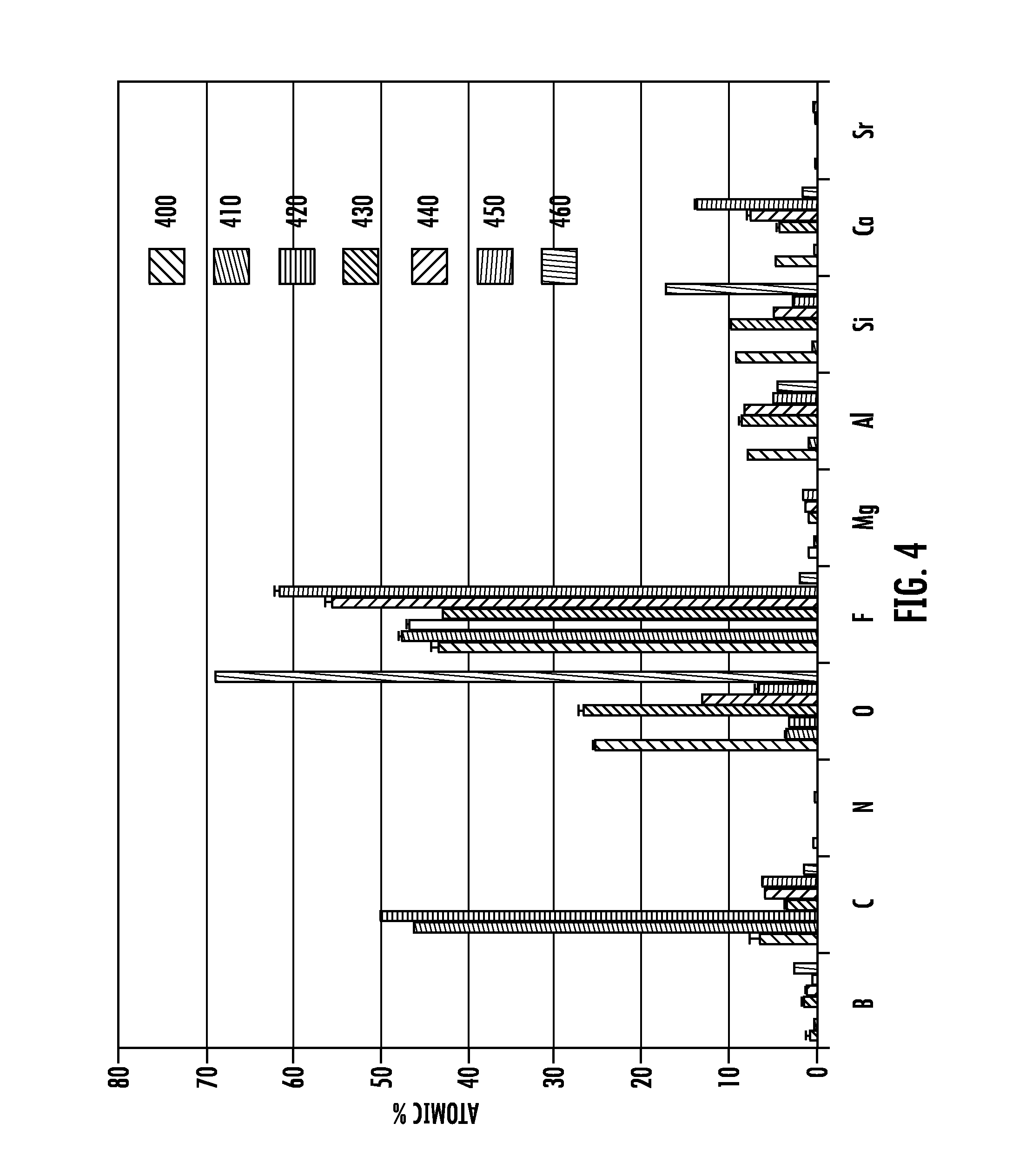
FIG. 4 shows the changes in elemental surface composition as measured by XPS as a function of different plasma treatment times. In each instance, the flow rate of the gas was 50 standard cubic centimeter per minute (sccm) at a pressure of 50 milli-torrs. The plasma treatment was either pure CHF.sub.3 or pure CF.sub.4 (400, 410, and 420 refer to 6 seconds, 60 seconds, and 600 seconds of CHF.sub.3 plasma treatments, respectively, and 430, 440, and 450 refer to 6 seconds, 60 seconds, and 600 seconds of CF.sub.4 plasma treatment times, respectively). The surface composition of untreated flat glass is also presented for comparison (460; negative control). The data shows that while for 6 seconds of plasma treatment, the surface concentration of carbon is less than 10 at %, the surface concentration of fluorine exceeds 40 at %.
FIG. 4 also shows that for CF.sub.4 plasma polymer surface treatments there is little increase in carbon or fluorine concentration after 6 seconds. Silicon, oxygen, and boron concentrations decrease with increasing CF.sub.4 plasma exposure time, while Al, Mg, Ca, and Sr concentrations increase with increasing CF.sub.4 plasma exposure time. This is consistent with CF.sub.4 plasma treatment etching the glass surface and depleting the surface of silicon, oxygen, and boron.
Changes in bond energy vs. anneal temperature and anneal time for CF.sub.4 and CHF.sub.3 plasma polymer treated Eagle XG.RTM. carrier bonded to SC1 cleaned thin glass is shown in FIG. 5A, and SC1 treated Eagle XG.RTM. carrier to SC1 treated thin glass is shown in FIG. 5B.
FIG. 5A shows the change in adhesion or bond energy as a function of the anneal temperature for RIE mode CF4 and CHF3 treated Eagle XG.RTM. carriers with three different surface energies prepared by changing the gas ratio as described in FIG. 2: at 40 mJ/m.sup.2 surface energy (510) the bond energy is too weak and is inadequate for surviving low temperature polysilicon (LTPS) processing. At 55 mJ/m.sup.2 surface energy (511) the bond energy is adequate to survive LPTS processing; and at 72 mJ/m.sup.2 the surface energy (512) is still adequate for surviving LTPS processing but is more difficult to peel off the flexible glass sheet from the carrier. The bond energy (SE) or adhesion limit (515) is about 2500 mJ per square meter where attempted separation results in glass breakage failure.
FIG. 5B shows the bond energy (SE) of an SC1 treated Eagle XG.RTM. carrier to SC1 treated thin glass or adhesion of a flexible glass sheet to the carrier in the laminate as a function of anneal time at 100.degree. C. (520), 150.degree. C. (521), 200.degree. C. (522), 250.degree. C. (523) and 300.degree. C. (524). Bond energy is observed to increase rapidly with increasing temperature. At 300.degree. C. (524), the thin glass was permanently bonded and could not be removed without breakage at annealing times of 10 min and above.
Bond energy (BE) measurements were accomplished using the wedge test method (see Tong, Q. Y., et al. "Semiconductor Wafer Bonding", Annu Rev Mater Sci, vol. 28, no. 1, pp. 215-241, 1998). The bond energy or adhesion between a surface treated carrier and a clean flexible glass can be determined by inserting a thin blade and measuring the crack length. The bond energy y is related to the carrier Young's modulus E.sub.1, carrier thickness t.sub.w1, flexible glass modulus E.sub.2, flexible glass thickness t.sub.w2, blade thickness t.sub.b, and crack length L by the equation:
.gamma..times..times..times..times..times..times..times..times..times..fu- nction..times..times..times..times..times..times. ##EQU00001##
From the examples in FIG. 5A it can be seen that creating a silicon and oxygen depleted and fluorine and carbon enhanced surface rich in alkaline earth fluorides by an inhomogeneous etching of glass surface optionally combined with polymer deposition can readily form temporary removable or releasable bonds to other high energy surfaces such as glass and in particular, thin glass.
In embodiments, a flexible glass sheet can have a thickness of from about 50 to about 300 microns, and a carrier glass article can have a of about 200 microns to 3 mm. Unexpectedly, this silicon and oxygen depleted and fluorine and carbon enriched surface does not permanently bond to glass surfaces at temperatures below about 600.degree. C.
The surface treatments described herein may be used to process thin wafers in semiconductor and/or interposer processing. Some examples of the present invention are generally directed to carriers bonded to and removed from thinner substrates to allow processing of the thinner substrates. More particularly, some examples of the present invention are directed to methods and apparatuses for bonding wafers to carriers for semiconductor and/or interposer processing, and then debonding the wafers from the carriers after such processing.
Semiconductor devices are fabricated by forming active devices on or within a semiconductor wafer. The semiconductor wafer may comprise, for example, glass, silicon, polysilicon, single crystal silicon, silicon oxide, aluminum oxide, combinations of these, and/or the like. Hundreds or thousands of integrated circuits (ICs) or dies are typically manufactured on a single wafer. Typically, a plurality of insulating, conductive, and semiconductive material layers are sequentially deposited and patterned over the wafer to form the ICs. One of the uppermost-formed material layers typically comprises a layer for bond pads which make electrical connection to the underlying active areas and components within the wafer.
After the ICs are formed, the wafer may be subjected to backside processing. The backside processing may include thinning the wafer to prepare the wafer for packaging. For example, in some technologies, backside processing may include forming electrical connections to through-substrate vias formed through the wafer for providing backside contacts. In this example, the backside of the wafer is thinned through a process such as grinding in order to expose the conductive vias on the backside of the wafer. This process of thinning the wafer can damage the edges of the wafer and can make the wafer even more fragile and susceptible to damage during subsequent transportation and processing of the wafer.
To help alleviate these types of damage, a carrier may be attached to the wafer. Typically, before, this carrier was attached using an adhesive, and was intended to allow handling of the wafer by handling the carrier. Additionally, the added strength of the carrier supports the wafer so that stresses caused by transportation and/or processing will not damage the wafer. A typical carrier may be a glass substrate attached to the wafer using an adhesive. It has been found, however, that the wafer may warp during processing and that the typical carrier does not provide sufficient support to prevent warping. As a result of the warpage of the wafer, processes may fail and/or cause alarm conditions. The first portion of the IC fabrication, where the active transistors, resistors and RC circuits, and local wiring to interconnect the transistors are patterned in the semiconductor, is called front-end-of-line (FEOL) processing. FEOL processing may also include: well formation; gate module formation; source and drain module formation; DRIE (dry reactive ion etch); PVD, Ti or Cu, or other; CVD TiN or other; PECVD SiO2, or other; Electrolytic Cu (or other) Plating; Cu (or other) annealing; Metrology (X-Ray or other); Cu (or other) CMP (Chemical Mechanical Polish); Cu (H2O2+H2SO4)+Ti (DHF) Wet Etch; Sputter Adhesion Layer (Ti or other); Sputter Seed Layer (Cu or other); Lithography (Photoresist, expose, strip, etch Cu). Due to some of the high temperature (e.g., .gtoreq.500.degree. C., in some instances, 500.degree. C. to 650.degree. C., and in some cases up to 700.degree. C.) processes associated with FEOL processing, many adhesive based solutions cannot be used, as they may fail to hold the bond, they may outgas contaminants, or both. Many adhesives even outgas at much lower temperatures, e.g., around 300.degree. C. The portion of IC fabrication line where the coarse wiring that connects longer distances across individual chip and goes to off chip locations are interconnected with wiring on the wafer is called back-end-of-line (BEOL) wiring. BEOL processing may also include one or more of formation of contacts, insulating layers, interconnect wiring, RF shielding, passivation, ESD protection, bonding pads and other bonding sites for chip-to-package solutions. Although BEOL processing temperatures are generally lower than FEOL processing temperatures, dielectric deposition typically occurs at 350-450.degree. C. and most adhesives outgas at these lower temperatures. Moreover, most temporary adhesives have high CTEs which are mismatched with the wafer and carrier materials, and are difficult to remove while leaving the delicate microstructures on the wafer intact. Additionally, the CTE mismatch between the adhesive and the wafer and/or carrier materials may cause undesirable warping of the wafer. Still further, adhesive may find its way into the vias of an interposer when bonding to a carrier and undesirably prevent metallization of at least part of the via.
Thus, there is a need for an improved carrier-substrate solution that can withstand processing conditions, particularly the high temperature demands of FEOL processing. Additionally, a carrier-substrate solution that can withstand the rigors of FEOL, and yet provide for easy debonding thereafter, will allow a thinner initial substrate to be used from the get-go, thereby alleviating the need for back-end thinning That is, typical existing semiconductor tools are designed to process wafers on the order of 500 microns and above. However, with a carrier supporting a wafer, the combined thickness need only be within the tools' processing thickness range. Thus, for example, a carrier having a thickness of 400 microns may be used to support a wafer of 100 microns, and the combination processed in the existing semiconductor tool. With the present solution, due to the controlled bonding that allows easy separation even after high temperature processing, 100 micron wafers may be used as substrates, thereby avoiding the waste and potential yield reductions of thinning after forming devices on the wafer. The ability to withstand FEOL processing will allow a carrier-substrate solution to start with a wafer having a thickness of .ltoreq.200 microns, for example, 200, 190, 180, 170, 160, 150, 140, 130, 120, 110, 100, 90, 80, 70, 60, 50, 40, 30, or 20 microns. The wafer of such a thickness (.ltoreq.200 microns for example) can be attached to a carrier, processed, and then removed from the carrier. This can be a major advantage when, for example, polysilicon or single crystal silicon wafers are used as the substrates because there can be avoided the removal and waste of a very expensive material; the material can simply be processed at its as-formed thickness.
Additionally, 3D IC technology has been widely accepted by the Semiconductor Industry as a major technology trend to improve performance of semiconductors without requiring ever more expensive advanced lithography solutions or requiring larger chip size to accommodate more circuitry. This technology for 3D ICs relies on thinned silicon ICs, and also on interposers to redistribute electrical signals between IC's directly on a single interposer in a planar configuration (2.5D IC) as well as to stack thinned IC's (3D IC).
These interposers, which can be made of polysilicon, single crystal silicon or glass, allow dramatic improvements in the speed of communications by reducing path lengths from millimeters to microns. The lead application for this new technology has been Field Programmable Gate Arrays (FPGA), a high end specialized functionality manufactured by Xilinx (San Jose, Calif., USA), for example.
Interposers are characteristically on the order of 50 um to 100 um thick, sized from 200 mm OD to 300 mm OD today, trending towards larger sized panels long term. The vias, through which electrical signals are processed following metallization, are from Sum OD to 150 um OD with a density typically 1 to 20 vias per square millimeter, depending on design and application. Interposers are by definition thin, as thick interposers cause an unacceptable form factor (height) and performance (heat) obstacles. Thin is generally regarded as around 100 microns, but generally not to exceed 200 microns. On the other end, the International Technology Roadmap for Semiconductors (ITRS) allows for thicknesses down to 50 um. Again, substrates of these thicknesses generally cannot be processed in existing tools. Thus, the present disclosure contemplates the advantageous use of a carrier, and one that may stay attached with the wafer even during high temperature processing, and yet still allow an easy release of the wafer after such processing.
Although the interposer technology is new, the dominant interposer substrate is single crystal silicon, with glass emerging as an alternative. The attractiveness of glass is performance and cost, but no solution has yet existed today to realize these advantages for glass. The concepts in the present disclosure will allow processing of a variety of thin substrates as wafers, including silicon and glass, as well as under a variety of conditions, including FEOL and BEOL, to provide a variety of devices including ICs, RC circuits, and interposers.
The bonding solutions of the present disclosure allow the processing of thin form at final thickness glass, as well as thinned Silicon, through all existing required process steps with high yield and with low processing time. After the thin wafer is processed through metallization, distribution layer placement, it can be debonded leaving the thinned and processed interposer, and/or IC, intact. Moreover, the use of carrier with an already-thinned (on the order of .ltoreq.200 microns) silicon wafer allows the wafer to be screened before any devices are processed thereon. Accordingly, costs can be reduced and/or yields improved.
In light of the above, there is a need for a thin sheet--carrier article that can withstand the rigors of the FEOL processing, including high temperature processing (without outgassing that would be incompatible with the semiconductor or display making processes in which it will be used), yet allow the entire area of the thin sheet to be removed (either all at once, or in sections) from the carrier. The present specification describes surface treatments to control the adhesion between the carrier and thin sheet to create a temporary bond sufficiently strong to survive FEOL processing (including high temperature processing) but weak enough to permit debonding of the sheet from the carrier, even after high-temperature processing. More specifically, the present disclosure provides surface treatments that may be provided on the thin sheet, the carrier, or both, to control both room-temperature van der Waals, and/or hydrogen, bonding and high temperature covalent bonding between the thin sheet and carrier. Even more specifically, the room-temperature bonding may be controlled so as to be sufficient to hold the thin sheet and carrier together during vacuum processing, wet processing, and/or ultrasonic cleaning processing. And at the same time, the high temperature covalent bonding may be controlled so as to prevent a permanent bond between the thin sheet and carrier during high temperature processing, as well as maintain a sufficient bond to prevent delamination during high temperature processing.
Another use of the surface treatments, which form the temporary bonding condition, is to provide for use of a thin sheet on a carrier to process the thin sheet in processes requiring a temperature .gtoreq.400.degree. C. (for example .gtoreq.450.degree. C., .gtoreq.500.degree. C., .gtoreq.550.degree. C., .gtoreq.600.degree. C.), as in FEOL processing, for example. That is, the thin sheet may be a wafer that is processed at thickness without having to thin it later on. Surface treatments as described herein may be used to provide reuse of the carrier under such temperature conditions. Specifically, these surface treatments may be used to form a temporary bond between the thin sheet and carrier, whereby the entire thin sheet may be separated from the carrier after processing. The thin sheet may be separated all at once, or may be separated in sections as, for example, when first removing devices produced on portions of the thin sheet and thereafter removing any remaining portions to clean the carrier for reuse, for example. In the event that the entire thin sheet is removed from the carrier, as by removal of the thin sheet as a whole, or as by removing diced sections of the thin sheet the sum of which add to the entire thin sheet, the carrier can be reused as is by simply by placing another thin sheet thereon. Alternatively, the carrier may be cleaned and once again prepared to carry a thin sheet by forming a surface treatment anew. Because the surface treatments provide a temporary bond between the thin sheet and the carrier, they may be used for processes wherein temperatures are .gtoreq.600.degree. C. Of course, although these surface treatments may control bonding surface energy during processing at temperatures .gtoreq.600.degree. C., they may also be used to produce a thin sheet and carrier combination that will withstand processing at lower temperatures, for example temperatures .gtoreq.400.degree. C. (for example .gtoreq.450.degree. C., .gtoreq.500.degree. C., .gtoreq.550.degree. C.), and may be used in such lower temperature applications to control bonding, for example in BEOL processing. The thin sheet may be a polysilicon or single crystal silicon wafer, silicon wafer, glass, ceramic, glass-ceramic, quartz, sapphire, having a thickness of .ltoreq.200 microns, and may be processed at, for example temperatures .gtoreq.500.degree. C. to form RC circuits, ICs, or other electronic devices thereon in FEOL processing. After FEOL processing, the wafer may easily be removed from the carrier without damaging the electronic devices. Before removal, however, the wafer may undergo further, lower temperature processing, as in BEOL processing, for example.
A second use of the surface treatments, to provide a temporary bond, is to fabricate an interposer. In this case, the thin sheet is an interposer, which may be a wafer made from any suitable material including silicon, polysilicon, single crystal silicon, glass, ceramic, glass-ceramic, quartz, sapphire, for example, and which may have a thickness of .ltoreq.200 microns, for example.
An example of an interposer, and the fabrication thereof, will now be described with reference to FIGS. 6-8.
With reference to FIG. 6, a thin sheet 20 may be bonded to a carrier 10 by a controlled bonding area 40, i.e., an area in which a temporary bond is formed between the thin sheet 20 and the carrier 10.
In this embodiment, the carrier 10, may be a glass substrate, or another suitable material having a similar surface energy as glass, for example, silicon, polysilicon, single crystal silicon, ceramic, glass-ceramic, sapphire, or quartz. An advantage of using a glass substrate is that flat sheets having minimal thickness variation can be obtained at a relatively low cost, avoiding the need for expensive carrier substrates. Additionally, with glass, a high quality can be achieved in a cost effective manner. That is, a very uniform thickness glass substrate can be made very cheaply, and used as a carrier. However, with the surface treatments of the present disclosure, the carrier need not be a high precision carrier having a low total thickness variation as in the case where the wafer will be thinned to final thickness. That is, when a wafer on a carrier will be thinned, the carrier must have a very tight control on total thickness variation because any variation in the carrier will be present in the thinned wafer upon thinning With the surface treatments of the present disclosure, which allow forming devices on the wafer when the wafer is already at final thickness, the total thickness variation of the carrier is much less important.
In this embodiment, the thin sheet 20 is used to form interposers 56. The sheet may be silicon, including polysilicon or a single crystal silicon wafer, quartz, sapphire, ceramic, or glass, for example. The sheet 20 may have a thickness of .ltoreq.200 microns. The interposers 56 each having a perimeter 52 and an array 50 of vias, wherein the array 50 has a perimeter 57. Although ten interposers 56 are shown, any suitable number--including one--may be disposed on one thin sheet 20. For convenience of illustration, each interposer 56 is shown as having only one array 50 of vias, but such need not be the case; instead any interposer 56 may have more than one array 50. Further, although each interposer is shown as having the same number of arrays 50, such need not be the case; any number (including zero) of the interposers may have the same number of arrays 50. Additionally, although the arrays 50 will typically have the same number and pattern of vias, such need not be the case. For convenience of illustration, vias 60 are shown on only one of the arrays 50 of one of the interposers 56, but such need not be the case, i.e., any one or more of the remaining interposers 56 may have one or more arrays 50 of vias 60.
Reference will now be made to FIG. 7, which is a cross-sectional view as taken along line 7-7 in FIG. 6. The vias 60 may include through vias or blind vias, i.e., vias that end within the thickness of the sheet 20. Vias 60 have a diameter 62, and are spaced at a pitch 64. Although the diameters 62 are shown as being the same, such need not be the case, i.e., there may be different diameter vias in one array 50 or in different arrays 50 on one interposer 56. The diameter 62 may be from 5 microns to 150 microns, for example. Similarly, although the vias 62 are spaced at the same pitch 64, such need not be the case, i.e., different pitches may be present in one array 50, or in different arrays 50 on one interposer 56 or in different interposers 56 on one thin sheet 20. The pitch may be such that there are from 1 to 20 vias per square millimeter, for example, and will depend upon the design and application of the interposer. Additionally, material 61 may be present in any one or more of the vias 60. The material 61 may be an electrically conductive material, an electrically insulating material, or a combination thereof. For example, a conductive material may be formed on the perimeter of the via, i.e., at its outside diameter 62, and either a different conductive material or an insulating material may be used to fill in the remainder of the via.
Reference will now be made to FIG. 8, which is a view similar to that in FIG. 7, but with devices/structures disposed on the interposer 56 and connected to via(s) 60. As shown in FIG. 8, a device 66 may be disposed over, and connected with, a plurality of vias 60. Device 66 may include integrated circuits; MEMS; microsensors; power semiconductors; light-emitting diodes; photonic circuits; CPU; SRAM; DRAM, eDRAM; ROM, EEPROM; flash memory; interposers; embedded passive devices; and microdevices fabricated on or from silicon, silicon-germanium, gallium arsenide, and gallium nitride. Although only one device 66 is shown, there may be any suitable number of devices 66 on one interposer 56, including an array of devices 56. Alternatively, a structure 68 may be disposed over and connected with only one via 60. Structures 68 may include: solder bumps; metal posts; metal pillars; interconnection routings; interconnect lines; insulating oxide layers; and structures formed from a material selected from the group consisting of silicon, polysilicon, silicon dioxide, silicon (oxy)nitride, metal (for example, Cu, Al, W), low k dielectrics, polymer dielectrics, metal nitrides, and metal silicides. Although only one structure 68 is shown, there may be any suitable number of structures 68 on one interposer 56, including array(s) of structures 56. Further, one or more structures 68 may be disposed on a device 66.
In the controlled bonding area 40, the carrier 10 and thin sheet 20 are bonded to one another so that over the entire area of overlap, the carrier 10 and thin sheet 20 are connected, but may be separated from one another, even after high temperature processing, e.g. processing at temperatures .gtoreq.400.degree. C., for example .gtoreq.450.degree. C., .gtoreq.500.degree. C., .gtoreq.550.degree. C., .gtoreq.600.degree. C., and on up to about 650.degree. C., or in some cases to 700.degree. C.
The surface treatments disclosed herein result in an interfacial bonding layer 30 to provide temporary bonding areas 40 between the carrier 10 and the thin sheet 20. Specifically, these surface treatments may be formed within the perimeters 52 of the arrays 50 either on the carrier 10 or on the thin sheet 20. Accordingly, when the article 2 is processed at high temperature during device processing, there can be provided a temporary bond between the carrier 10 and the thin sheet 20 within the areas bounded by perimeters 52 whereby a separation force may separate (without catastrophic damage to the thin sheet or carrier) the thin sheet and carrier in this region, yet the thin sheet and carrier will not delaminate during processing, including ultrasonic processing. Additionally, because of the very small thickness of the interfacial bonding layer 30, i.e., less than 100 nanometers, less than 40 nanometers, less than 10 nanometers, and in some instances about 2 nanometers, there is no effect on the wafer due to CTE mismatch between the wafer and the surface treatment (as there is in the case of thicker adhesive layers, i.e., on the order of 40-60 microns or more).
Then, during extraction of the interposers 56 (each having an array 50 of vias 60) having perimeters 52, the portions of thin sheet 20 within the perimeters 52 may simply be separated from the carrier 10 after processing and after separation of the thin sheet along perimeters 52. Alternatively, the thin sheet 20 (and alternatively both the thin sheet 20 and the carrier 10) may be diced along lines 5, whereby a section of the thin sheet 20 larger than the interposer 56 perimeter 52 may be removed from the carrier 10, or sections of the carrier 10 as in the event that the carrier is diced together with the thin sheet 20. Because the surface treatments provide temporary bonding of the thin sheet with the carrier, they may be used for processes wherein temperatures are .gtoreq.600.degree. C. Of course, although these surface treatments may control bonding surface energy during processing at temperatures .gtoreq.600.degree. C., they may also be used to produce a thin sheet and carrier combination that will withstand processing at lower temperatures for example .gtoreq.400.degree. C. (for example .gtor
uspto.report is an independent third-party trademark research tool that is not affiliated, endorsed, or sponsored by the United States Patent and Trademark Office (USPTO) or any other governmental organization. The information provided by uspto.report is based on publicly available data at the time of writing and is intended for informational purposes only.
While we strive to provide accurate and up-to-date information, we do not guarantee the accuracy, completeness, reliability, or suitability of the information displayed on this site. The use of this site is at your own risk. Any reliance you place on such information is therefore strictly at your own risk.
All official trademark data, including owner information, should be verified by visiting the official USPTO website at www.uspto.gov. This site is not intended to replace professional legal advice and should not be used as a substitute for consulting with a legal professional who is knowledgeable about trademark law.