Restricted capacitor switching
Bhutta , et al. Nov
U.S. patent number 10,483,090 [Application Number 16/029,742] was granted by the patent office on 2019-11-19 for restricted capacitor switching. This patent grant is currently assigned to RENO TECHNOLOGIES, INC.. The grantee listed for this patent is Reno Technologies, Inc.. Invention is credited to Imran Ahmed Bhutta, Tomislav Lozic.


View All Diagrams
| United States Patent | 10,483,090 |
| Bhutta , et al. | November 19, 2019 |
Restricted capacitor switching
Abstract
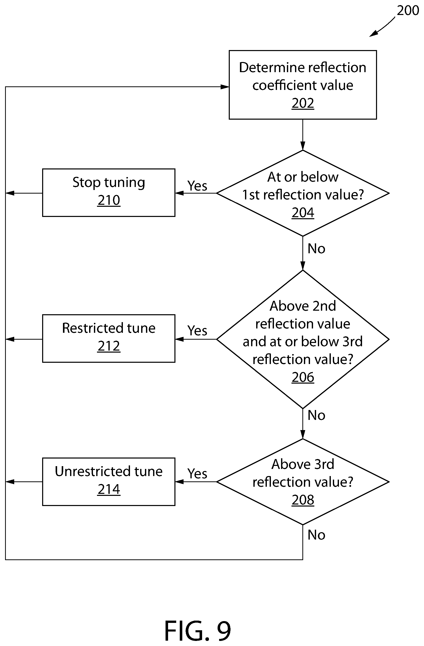
In one embodiment, the present disclosure is directed to a method for matching an impedance. The method can include determining or receiving a reflection parameter value at an RF input or output; stopping the altering of a first capacitance and a second capacitance when the reflection parameter value is at or below a first reflection value; causing a limited altering of the first capacitance and the second capacitance to pursue an impedance match when the reflection parameter value is at or above a second reflection value and at or below the third reflection value; and causing an unlimited altering of the first capacitance and the second capacitance to pursue an impedance match when the reflection parameter value is at or above a third reflection value.
| Inventors: | Bhutta; Imran Ahmed (Moorestown, NJ), Lozic; Tomislav (Gilbert, AZ) | ||||||||||
|---|---|---|---|---|---|---|---|---|---|---|---|
| Applicant: |
|
||||||||||
| Assignee: | RENO TECHNOLOGIES, INC.
(Wilmington, DE) |
||||||||||
| Family ID: | 64903826 | ||||||||||
| Appl. No.: | 16/029,742 | ||||||||||
| Filed: | July 9, 2018 |
Prior Publication Data
| Document Identifier | Publication Date | |
|---|---|---|
| US 20190013183 A1 | Jan 10, 2019 | |
Related U.S. Patent Documents
| Application Number | Filing Date | Patent Number | Issue Date | ||
|---|---|---|---|---|---|
| 62530446 | Jul 10, 2017 | ||||
| Current U.S. Class: | 1/1 |
| Current CPC Class: | H03H 11/28 (20130101); H03H 7/40 (20130101); H01J 37/32183 (20130101); H01J 2237/24564 (20130101); H01L 21/67069 (20130101); H01J 2237/332 (20130101); H01J 2237/334 (20130101) |
| Current International Class: | H03H 7/38 (20060101); H01J 37/32 (20060101); H03H 11/28 (20060101); H03H 7/40 (20060101); H01L 21/67 (20060101) |
| Field of Search: | ;333/17.3,32,33,99PL |
References Cited [Referenced By]
U.S. Patent Documents
| 3828281 | August 1974 | Chambers |
| 4110700 | August 1978 | Rosen et al. |
| 4679007 | July 1987 | Reese et al. |
| 4692643 | September 1987 | Tokunaga et al. |
| 4751408 | June 1988 | Rambert |
| 4929855 | May 1990 | Ezzeddine |
| 5012123 | April 1991 | Ayasli et al. |
| 5079507 | January 1992 | Ishida et al. |
| 5654679 | August 1997 | Mavretic et al. |
| 5815047 | September 1998 | Sorensen et al. |
| 5849136 | December 1998 | Mintz et al. |
| 5880921 | March 1999 | Tham et al. |
| 5889252 | March 1999 | Williams et al. |
| 5971591 | October 1999 | Vona et al. |
| 6046641 | April 2000 | Chawla et al. |
| 6137367 | October 2000 | Ezzedine et al. |
| 6252354 | June 2001 | Collins et al. |
| 6400012 | June 2002 | Miller et al. |
| 6424232 | July 2002 | Mavretic et al. |
| 6583572 | June 2003 | Veltrop et al. |
| 6621372 | September 2003 | Kondo et al. |
| 6657395 | December 2003 | Windhorn |
| 6677828 | January 2004 | Harnett et al. |
| 6703080 | March 2004 | Reyzelman et al. |
| 6791274 | September 2004 | Hauer et al. |
| 6794951 | September 2004 | Finley |
| 6818562 | November 2004 | Todorow et al. |
| 6888313 | May 2005 | Blackburn et al. |
| 6888396 | May 2005 | Hajimiri et al. |
| 6946847 | September 2005 | Nishimori et al. |
| 6967547 | November 2005 | Pellegrini et al. |
| 7004107 | February 2006 | Raoux et al. |
| RE39051 | March 2006 | Harnett |
| 7071786 | July 2006 | Inoue et al. |
| 7095178 | August 2006 | Nakano et al. |
| 7113761 | September 2006 | Bickham et al. |
| 7122965 | October 2006 | Goodman |
| 7164236 | January 2007 | Mitrovic et al. |
| 7199678 | April 2007 | Matsuno |
| 7251121 | July 2007 | Bhutta |
| 7298091 | November 2007 | Pickard et al. |
| 7298128 | November 2007 | Bhutta |
| 7304438 | December 2007 | Kishinevsky |
| 7332981 | February 2008 | Matsuno |
| 7439610 | October 2008 | Weigand |
| 7480571 | January 2009 | Howald et al. |
| 7495524 | February 2009 | Omae et al. |
| 7498908 | March 2009 | Gurov |
| 7514935 | April 2009 | Pankratz |
| 7518466 | April 2009 | Sorensen et al. |
| 7535312 | May 2009 | McKinzie, III |
| 7602127 | October 2009 | Coumou |
| 7642879 | January 2010 | Matsuno |
| 7666464 | February 2010 | Collins et al. |
| 7714676 | May 2010 | McKinzie, III |
| 7728602 | June 2010 | Valcore et al. |
| 7745955 | June 2010 | Kirchmeier et al. |
| 7755300 | July 2010 | Kishinevsky et al. |
| 7764140 | July 2010 | Nagarkatti et al. |
| 7777567 | August 2010 | Polizze |
| 7852170 | December 2010 | McKinzie, III |
| 7863996 | January 2011 | Cotter et al. |
| 7868556 | January 2011 | Xia |
| 7872523 | January 2011 | Sivakumar et al. |
| 7917104 | March 2011 | Manssen et al. |
| 7969096 | June 2011 | Chen |
| 8008982 | August 2011 | McKinzie, III |
| 8040068 | October 2011 | Coumou et al. |
| RE42917 | November 2011 | Hauer et al. |
| 8089026 | January 2012 | Sellers |
| 8102954 | January 2012 | Coumou |
| 8110991 | February 2012 | Coumou |
| 8203859 | June 2012 | Omae et al. |
| 8217731 | July 2012 | McKinzie, III |
| 8217732 | July 2012 | McKinzie, III |
| 8228112 | July 2012 | Reynolds |
| 8237501 | August 2012 | Owen |
| 8264154 | September 2012 | Banner et al. |
| 8278909 | October 2012 | Fletcher |
| 8289029 | October 2012 | Coumou |
| 8299867 | October 2012 | McKinzie, III |
| 8314561 | November 2012 | Fisk et al. |
| 8330432 | December 2012 | Van Zyl et al. |
| 8334657 | December 2012 | Xia |
| 8334700 | December 2012 | Coumou et al. |
| 8335479 | December 2012 | Koya et al. |
| 8344559 | January 2013 | Van Zyl et al. |
| 8344801 | January 2013 | Owen et al. |
| 8368308 | February 2013 | Banna et al. |
| 8368469 | February 2013 | Mohammadi et al. |
| 8395322 | March 2013 | Coumou |
| 8416008 | April 2013 | Van Zyl et al. |
| 8436643 | May 2013 | Mason |
| 8461842 | June 2013 | Thuringer et al. |
| 8466736 | June 2013 | Reynolds |
| 8487706 | July 2013 | Li et al. |
| 8502689 | August 2013 | Chen et al. |
| 8513889 | August 2013 | Zhang et al. |
| 8520413 | August 2013 | Tran et al. |
| 8536636 | September 2013 | Englekirk |
| 8552665 | October 2013 | Larson et al. |
| 8558633 | October 2013 | McKinzie, III |
| 8559907 | October 2013 | Burgener et al. |
| 8564381 | October 2013 | McKinzie |
| 8569842 | October 2013 | Weis et al. |
| 8576010 | November 2013 | Yanduru |
| 8576013 | November 2013 | Coumou |
| 8587321 | November 2013 | Chen et al. |
| 8620236 | December 2013 | Manssen et al. |
| 8624501 | January 2014 | Nagarkatti et al. |
| 8633782 | January 2014 | Nagarkatti et al. |
| 8638159 | January 2014 | Ranta et al. |
| 8649754 | February 2014 | Burgener et al. |
| 8659335 | February 2014 | Nagarkatti et al. |
| 8674606 | March 2014 | Carter et al. |
| 8680928 | March 2014 | Jeon et al. |
| 8686796 | April 2014 | Presti |
| 8710926 | April 2014 | Nagarkatti et al. |
| 8716984 | May 2014 | Mueller et al. |
| 8723423 | May 2014 | Hoffman et al. |
| 8742669 | June 2014 | Carter et al. |
| 8773019 | July 2014 | Coumou et al. |
| 8779859 | July 2014 | Su et al. |
| 8781415 | July 2014 | Coumou et al. |
| 8815329 | August 2014 | Ilic et al. |
| 8847561 | September 2014 | Karlieek et al. |
| 8884180 | November 2014 | Ilic et al. |
| 8884525 | November 2014 | Hoffman et al. |
| 8890537 | November 2014 | Valcore, Jr. et al. |
| 8912835 | December 2014 | Nagarkatti et al. |
| 8928329 | January 2015 | Downing et al. |
| 9083343 | July 2015 | Li et al. |
| 9190993 | November 2015 | Li |
| 9306533 | April 2016 | Anton |
| 2002/0060914 | May 2002 | Porter et al. |
| 2003/0007372 | January 2003 | Porter et al. |
| 2003/0046013 | March 2003 | Gerrish |
| 2006/0170367 | August 2006 | Bhutta |
| 2006/0198077 | September 2006 | Bhutta |
| 2006/0232471 | October 2006 | Coumou |
| 2007/0075784 | April 2007 | Pettersson et al. |
| 2007/0139122 | June 2007 | Nagarkatti et al. |
| 2008/0179948 | July 2008 | Nagarkatti et al. |
| 2008/0180179 | July 2008 | Polizzo |
| 2008/0197854 | August 2008 | Valcore et al. |
| 2009/0207537 | August 2009 | Coumou |
| 2010/0001796 | January 2010 | Sivakumar et al. |
| 2010/0073104 | March 2010 | Cotter et al. |
| 2010/0123502 | May 2010 | Bhutta et al. |
| 2010/0194195 | August 2010 | Coumou et al. |
| 2010/0201370 | August 2010 | Coumou et al. |
| 2010/0231296 | September 2010 | Nagarkatti et al. |
| 2011/0241781 | October 2011 | Owen et al. |
| 2011/0247696 | October 2011 | Zolock et al. |
| 2012/0013253 | January 2012 | Coumou |
| 2012/0062322 | March 2012 | Owen |
| 2012/0188007 | July 2012 | Van Zyl et al. |
| 2012/0262064 | October 2012 | Nagarkatti et al. |
| 2013/0043854 | February 2013 | Tran et al. |
| 2013/0169359 | July 2013 | Coumou |
| 2013/0193867 | August 2013 | Van Zyl et al. |
| 2013/0207738 | August 2013 | Mason |
| 2013/0222055 | August 2013 | Coumou et al. |
| 2013/0257311 | October 2013 | Tran et al. |
| 2013/0314163 | November 2013 | Costa |
| 2013/0320853 | December 2013 | Carter et al. |
| 2014/0009248 | January 2014 | Granger-Jones |
| 2014/0028389 | January 2014 | Coumou |
| 2014/0028398 | January 2014 | Owen |
| 2014/0049250 | February 2014 | Brown et al. |
| 2014/0055034 | February 2014 | Coumou |
| 2014/0061156 | March 2014 | Brouk et al. |
| 2014/0062303 | March 2014 | Hoffman et al. |
| 2014/0097908 | April 2014 | Fisk, II et al. |
| 2014/0117861 | May 2014 | Finley et al. |
| 2014/0117872 | May 2014 | Finley |
| 2014/0118031 | May 2014 | Rughoonundon et al. |
| 2014/0210345 | July 2014 | Hoffman |
| 2014/0210551 | July 2014 | Mueller |
| 2014/0218076 | August 2014 | Coumou et al. |
| 2014/0220913 | August 2014 | Coumou et al. |
| 2014/0231243 | August 2014 | Finley |
| 2014/0232266 | August 2014 | Finley et al. |
| 2014/0266492 | September 2014 | Radomski et al. |
| 2014/0306742 | October 2014 | Menzer et al. |
| 2014/0320013 | October 2014 | Coumou et al. |
| 2015/0115289 | April 2015 | Fursin et al. |
| 0840349 | May 1998 | EP | |||
| 0840350 | May 1998 | EP | |||
| 2006096589 | Sep 2006 | WO | |||
Attorney, Agent or Firm: The Belles Group, P.C.
Parent Case Text
CROSS REFERENCE TO RELATED APPLICATIONS
The present application claims the benefit of U.S. Provisional Patent Application No. 62/530,446, filed Jul. 10, 2017, which is incorporated herein by reference.
Claims
What is claimed is:
1. An impedance matching network, the network comprising: a radio frequency (RF) input configured to operably couple to an RF source; an RF output configured to operably couple to a plasma chamber; a first electronically variable capacitor (EVC) comprising discrete capacitors configured to be switched in and out to alter a first capacitance of the first EVC; a second EVC comprising discrete capacitors configured to be switched in and out to alter a second capacitance of the second EVC; and a control circuit operably coupled to the first and second EVCs, the control circuit configured to: determine or receive a reflection parameter value at the RF input or the RF output; stop the altering of the first capacitance and the second capacitance when the reflection parameter value is at or below a first reflection value; cause a limited altering of the first capacitance and the second capacitance to pursue an impedance match when the reflection parameter value is (a) at or above a second reflection value and (b) at or below the third reflection value, the limited altering allowing only a predetermined number of predetermined discrete capacitors to switch in or out; and cause an unlimited altering of the first capacitance and the second capacitance to pursue an impedance match when the reflection parameter value is at or above a third reflection value, the unlimited altering allowing any discrete capacitor of the first or second EVC to switch in or out.
2. The matching network of claim 1 wherein the reflection parameter value is a load impedance at the RF output.
3. The matching network of claim 1 wherein the control circuit is further configured to continuously monitor the reflection parameter value.
4. The matching network of claim 1 wherein the discrete capacitors of each of the first EVC and the second EVC comprise coarse and fine capacitors, wherein the coarse capacitors have a capacitance at least twice as large as the capacitance of the fine capacitors, and wherein the predetermined discrete capacitors are fine capacitors.
5. The matching network of claim 4 wherein the predetermined number is two.
6. The matching network of claim 1 wherein the reflection parameter value is a reflection coefficient value representing a ratio of an amplitude of a reflected wave to an incident wave at the RF input or the RF output.
7. The matching network of claim 6 wherein the reflection coefficient value is determined based on a sensor signal from a sensor at the RF input.
8. The matching network of claim 1 wherein the control circuit is further configured to, before altering the first capacitance or the second capacitance, determine a positioning for the discrete capacitors to achieve an impedance match, the limited altering preventing the determined positioning of the discrete capacitors from being fully carried out.
9. The matching network of claim 8 wherein the unlimited altering allows the determined positioning of the discrete capacitors to be fully carried out.
10. A semiconductor processing tool comprising: a plasma chamber configured to deposit a material onto a substrate or etch a material from the substrate; and an impedance matching network operably coupled to the plasma chamber, the matching network comprising: a radio frequency (RF) input configured to operably couple to an RF source; an RF output configured to operably couple to the plasma chamber; a first electronically variable capacitor (EVC) comprising discrete capacitors configured to be switched in and out to alter a first capacitance of the first EVC; a second EVC comprising discrete capacitors configured to be switched in and out to alter a second capacitance of the second EVC; and a control circuit operably coupled to the first and second EVCs, the control circuit configured to: determine or receive a reflection parameter value at the RF input or the RF output; stop the altering of the first capacitance and the second capacitance when the reflection parameter value is at or below a first reflection value; cause a limited altering of the first capacitance and the second capacitance to pursue an impedance match when the reflection parameter value is (a) at or above a second reflection value and (b) at or below the third reflection value, the limited altering allowing only a predetermined number of predetermined discrete capacitors to switch in or out; and cause an unlimited altering of the first capacitance and the second capacitance to pursue an impedance match when the reflection parameter value is at or above a third reflection value, the unlimited altering allowing any discrete capacitor of the first or second EVC to switch in or out.
11. The processing tool of claim 10 wherein the discrete capacitors of each of the first EVC and the second EVC comprise coarse and fine capacitors, wherein the coarse capacitors have a capacitance at least twice as large as the capacitance of the fine capacitors, and wherein the predetermined discrete capacitors are fine capacitors.
12. The processing tool of claim 10 wherein the reflection parameter value is a reflection coefficient value representing a ratio of an amplitude of a reflected wave to an incident wave at the RF input or the RF output.
13. The processing tool of claim 10 wherein the reflection parameter value is a load impedance at the RF output.
14. The processing tool of claim 10 wherein the control circuit is further configured to, before altering the first capacitance or the second capacitance, determine a positioning for the discrete capacitors to achieve an impedance match, the limited altering preventing the determined positioning of the discrete capacitors from being fully carried out.
15. A method of matching an impedance comprising: operably coupling a radio frequency (RF) input of a matching network to an RF source; operably coupling an RF output of the matching network to a plasma chamber, the plasma chamber comprising (a) a first electronically variable capacitor (EVC) comprising discrete capacitors configured to be switched in and out to alter a first capacitance of the first EVC, and (b) a second EVC comprising discrete capacitors configured to be switched in and out to alter a second capacitance of the second EVC; and determining or receiving a reflection parameter value at the RF input or the RF output; stopping the altering of the first capacitance and the second capacitance when the reflection parameter value is at or below a first reflection value; causing a limited altering of the first capacitance and the second capacitance to pursue an impedance match when the reflection parameter value is (a) at or above a second reflection value and (b) at or below the third reflection value, the limited altering allowing only a predetermined number of predetermined discrete capacitors to switch in or out; and causing an unlimited altering of the first capacitance and the second capacitance to pursue an impedance match when the reflection parameter value is at or above a third reflection value, the unlimited altering allowing any discrete capacitor of the first or second EVC to switch in or out.
16. The method of claim 15 wherein the discrete capacitors of each of the first EVC and the second EVC comprise coarse and fine capacitors, wherein the coarse capacitors have a capacitance at least twice as large as the capacitance of the fine capacitors, and wherein the predetermined discrete capacitors are fine capacitors.
17. The method of claim 15 wherein the reflection parameter value is a reflection coefficient value representing a ratio of an amplitude of a reflected wave to an incident wave at the RF input or the RF output.
18. The method of claim 15 wherein the reflection parameter value is a load impedance at the RF output.
19. The method of claim 15 further comprising, before altering the first capacitance or the second capacitance, determining a positioning for the discrete capacitors to achieve an impedance match, the limited altering preventing the determined positioning of the discrete capacitors from being fully carried out.
20. A method of manufacturing a semiconductor, the method comprising: placing a substrate in a plasma chamber configured to deposit a material layer onto the substrate or etch a material layer from the substrate; and coupling an impedance matching circuit between a radio frequency (RF) source and the plasma chamber, the impedance matching circuit comprising: a radio frequency (RF) input configured to operably couple to an RF source; an RF output configured to operably couple to a plasma chamber; a first electronically variable capacitor (EVC) comprising discrete capacitors configured to be switched in and out to alter a first capacitance of the first EVC; a second EVC comprising discrete capacitors configured to be switched in and out to alter a second capacitance of the second EVC; and a control circuit operably coupled to the first and second EVCs, the control circuit configured to: determine or receive a reflection parameter value at the RF input or the RF output; stop the altering of the first capacitance and the second capacitance when the reflection parameter value is at or below a first reflection value; cause a limited altering of the first capacitance and the second capacitance to pursue an impedance match when the reflection parameter value is (a) at or above a second reflection value and (b) at or below the third reflection value, the limited altering allowing only a predetermined number of predetermined discrete capacitors to switch in or out; and cause an unlimited altering of the first capacitance and the second capacitance to pursue an impedance match when the reflection parameter value is at or above a third reflection value, the unlimited altering allowing any discrete capacitor of the first or second EVC to switch in or out.
Description
BACKGROUND
The semiconductor device fabrication process uses plasma processing at different stages of fabrication to make a semiconductor device such as a microprocessor, a memory chip, or another integrated circuit or device. Plasma processing involves energizing a gas mixture by imparting energy to the gas molecules by the introduction of RF (radio frequency) energy into the gas mixture. This gas mixture is typically contained in a vacuum chamber, also called a plasma chamber, and the RF energy is introduced through electrodes or other means in the chamber. In a typical plasma process, the RF generator generates power at the desired RF frequency and power, and this power is transmitted through the RF cables and networks to the plasma chamber.
To provide efficient transfer of power from the RF generator to the plasma chamber, an RF matching network is positioned between the RF generator and the plasma chamber. The purpose of the RF matching network is to transform the plasma impedance to a value suitable for the RF generator. In many cases, particularly in the semiconductor fabrication processes, the RF power is transmitted through 50 Ohm coaxial cables and the system impedance (output impedance) of the RF generators is also 50 Ohm. On the other hand, the impedance of the plasma, driven by the RF power, varies. The impedance on the input side of the RF matching network must be transformed to non-reactive 50 Ohm (i.e., 50+j0) for maximum power transmission. RF matching network perform this task of continuously transforming the plasma impedance to 50 Ohm for the RF generator.
A typical RF matching network is composed of variable capacitors and a microprocessor-based control circuit to control the capacitors. The value and size of the variable capacitors are influenced by the power handling capability, frequency of operation, and impedance range of the plasma chamber. The predominant variable capacitor in use in RF matching networks is the vacuum variable capacitor (VVC). The VVC is an electromechanical device, consisting of two concentric metallic rings that move in relation to each other to change the capacitance. In complex semiconductor processes, where the impedance changes are very rapid, the rapid and frequent movements put stresses on the VVC leading to their failures. VVC-based RF matching networks are one of the last electromechanical components in the semiconductor fabrication process.
As semiconductor devices shrink in size and become more complex, however, the feature geometries become very small. As a result, the processing time to fabricate these features becomes small, typically in the 5-6 second range. Current RF matching networks take 1-2 seconds to tune the process and this results in unstable process parameters for a significant portion of the process time. Electronically variable capacitor (EVC) technology (see, e.g., U.S. Pat. No. 7,251,121, incorporated herein by reference) enables a reduction in this semiconductor processing tune time from 1-2 seconds to less than 500 seconds. EVC-based matching networks are a type of solid state matching networks. Their decreased tune time greatly increases the available stable processing time, thereby improving yield and performance.
While mechanical RF matching networks, such as VVC-based matching networks, cannot respond to rapid impedance changes, solid state RF matching networks, such as EVC-based matching networks, are able to respond to load impedance changes in a micro-second time frame. While this rapid response time is advantageous in applications such as when matching the load impedance of a semiconductor plasma, it can sometimes result in making the plasma instabilities worse by rapidly responding to impedance changes which may be so timed that the changes in the solid-state matching network form a positive feedback. To prevent further destabilizing a plasma load, but still providing a rapid response to match the plasma load impedance, a new matching algorithm is needed.
BRIEF SUMMARY
The present disclosure may be directed, in one aspect, to an impedance matching network, the network comprising a radio frequency (RF) input configured to operably couple to an RF source; an RF output configured to operably couple to a plasma chamber; a first electronically variable capacitor (EVC) comprising discrete capacitors configured to be switched in and out to alter a first capacitance of the first EVC; a second EVC comprising discrete capacitors configured to be switched in and out to alter a second capacitance of the second EVC; and a control circuit operably coupled to the first and second EVCs, the control circuit configured to determine or receive a reflection parameter value at the RF input or the RF output; stop the altering of the first capacitance and the second capacitance when the reflection parameter value is at or below a first reflection value; cause a limited altering of the first capacitance and the second capacitance to pursue an impedance match when the reflection parameter value is (a) at or above a second reflection value and (b) at or below the third reflection value, the limited altering allowing only a predetermined number of predetermined discrete capacitors to switch in or out; and cause an unlimited altering of the first capacitance and the second capacitance to pursue an impedance match when the reflection parameter value is at or above a third reflection value, the unlimited altering allowing any discrete capacitor of the first or second EVC to switch in or out.
In another aspect, the present disclosure may be directed to a method of matching an impedance comprising operably coupling a radio frequency (RF) input of a matching network to an RF source; operably coupling an RF output of the matching network to a plasma chamber, the plasma chamber comprising (a) a first electronically variable capacitor (EVC) comprising discrete capacitors configured to be switched in and out to alter a first capacitance of the first EVC, and (b) a second EVC comprising discrete capacitors configured to be switched in and out to alter a second capacitance of the second EVC; and determining or receiving a reflection parameter value at the RF input or the RF output; stopping the altering of the first capacitance and the second capacitance when the reflection parameter value is at or below a first reflection value; causing a limited altering of the first capacitance and the second capacitance to pursue an impedance match when the reflection parameter value is (a) at or above a second reflection value and (b) at or below the third reflection value, the limited altering allowing only a predetermined number of predetermined discrete capacitors to switch in or out; and causing an unlimited altering of the first capacitance and the second capacitance to pursue an impedance match when the reflection parameter value is at or above a third reflection value, the unlimited altering allowing any discrete capacitor of the first or second EVC to switch in or out.
In another aspect, the present disclosure may be directed to a semiconductor processing tool comprising a plasma chamber configured to deposit a material onto a substrate or etch a material from the substrate; and an impedance matching network operably coupled to the plasma chamber, the matching network comprising a radio frequency (RF) input configured to operably couple to an RF source; an RF output configured to operably couple to the plasma chamber; a first electronically variable capacitor (EVC) comprising discrete capacitors configured to be switched in and out to alter a first capacitance of the first EVC; a second EVC comprising discrete capacitors configured to be switched in and out to alter a second capacitance of the second EVC; and a control circuit operably coupled to the first and second EVCs, the control circuit configured to determine or receive a reflection parameter value at the RF input or the RF output; stop the altering of the first capacitance and the second capacitance when the reflection parameter value is at or below a first reflection value; cause a limited altering of the first capacitance and the second capacitance to pursue an impedance match when the reflection parameter value is (a) at or above a second reflection value and (b) at or below the third reflection value, the limited altering allowing only a predetermined number of predetermined discrete capacitors to switch in or out; and cause an unlimited altering of the first capacitance and the second capacitance to pursue an impedance match when the reflection parameter value is at or above a third reflection value, the unlimited altering allowing any discrete capacitor of the first or second EVC to switch in or out.
In another aspect, the present disclosure may be directed to a method of manufacturing a semiconductor, the method comprising placing a substrate in a plasma chamber configured to deposit a material layer onto the substrate or etch a material layer from the substrate; and coupling an impedance matching circuit between a radio frequency (RF) source and the plasma chamber, the impedance matching circuit comprising a radio frequency (RF) input configured to operably couple to an RF source; an RF output configured to operably couple to a plasma chamber; a first electronically variable capacitor (EVC) comprising discrete capacitors configured to be switched in and out to alter a first capacitance of the first EVC; a second EVC comprising discrete capacitors configured to be switched in and out to alter a second capacitance of the second EVC; and a control circuit operably coupled to the first and second EVCs, the control circuit configured to determine or receive a reflection parameter value at the RF input or the RF output; stop the altering of the first capacitance and the second capacitance when the reflection parameter value is at or below a first reflection value; cause a limited altering of the first capacitance and the second capacitance to pursue an impedance match when the reflection parameter value is (a) at or above a second reflection value and (b) at or below the third reflection value, the limited altering allowing only a predetermined number of predetermined discrete capacitors to switch in or out; and cause an unlimited altering of the first capacitance and the second capacitance to pursue an impedance match when the reflection parameter value is at or above a third reflection value, the unlimited altering allowing any discrete capacitor of the first or second EVC to switch in or out.
BRIEF DESCRIPTION OF THE DRAWINGS
The present disclosure will become more fully understood from the detailed description and the accompanying drawings, wherein:
FIG. 1 is a block diagram of an embodiment of a semiconductor processing system;
FIG. 2 is a block diagram of an embodiment of a semiconductor processing system having an L-configuration matching network;
FIG. 3 is a block diagram of an embodiment of a semiconductor processing system having a pi-configuration matching network;
FIG. 4 is a block diagram of an embodiment of an electronic circuit for providing a variable capacitance using an electronically variable capacitor having two capacitor arrays;
FIG. 5 is a block diagram of an embodiment of a variable capacitance system for switching in and out discrete capacitors of an electronically variable capacitor;
FIG. 6 is a flow chart showing an embodiment of a process for matching an impedance by altering a variable capacitance;
FIG. 7 is a flow chart showing another embodiment of a process for matching an impedance using a parameter matrix to alter a variable capacitance;
FIG. 8 is a flow chart showing another embodiment of a process for matching an impedance where a frequency of an RF source is also altered; and
FIG. 9 is a flow chart showing another embodiment of a process for matching an impedance where capacitor switching can be restricted.
DETAILED DESCRIPTION
The following description of the preferred embodiment(s) is merely exemplary in nature and is in no way intended to limit the invention or inventions. The description of illustrative embodiments is intended to be read in connection with the accompanying drawings, which are to be considered part of the entire written description. In the description of the exemplary embodiments disclosed herein, any reference to direction or orientation is merely intended for convenience of description and is not intended in any way to limit the scope of the present inventions. The discussion herein describes and illustrates some possible non-limiting combinations of features that may exist alone or in other combinations of features. Furthermore, as used herein, the term "or" is to be interpreted as a logical operator that results in true whenever one or more of its operands are true. Furthermore, as used herein, the phrase "based on" is to be interpreted as meaning "based at least in part on," and therefore is not limited to an interpretation of "based entirely on."
Features of the present inventions may be implemented in software, hardware, firmware, or combinations thereof. The computer programs described herein are not limited to any particular embodiment, and may be implemented in an operating system, application program, foreground or background processes, driver, or any combination thereof. The computer programs may be executed on a single computer or server processor or multiple computer or server processors.
Processors described herein may be any central processing unit (CPU), microprocessor, micro-controller, computational, or programmable device or circuit configured for executing computer program instructions (e.g., code). Various processors may be embodied in computer and/or server hardware of any suitable type (e.g., desktop, laptop, notebook, tablets, cellular phones, etc.) and may include all the usual ancillary components necessary to form a functional data processing device including without limitation a bus, software and data storage such as volatile and non-volatile memory, input/output devices, graphical user interfaces (GUIs), removable data storage, and wired and/or wireless communication interface devices including Wi-Fi, Bluetooth, LAN, etc.
Computer-executable instructions or programs (e.g., software or code) and data described herein may be programmed into and tangibly embodied in a non-transitory computer-readable medium that is accessible to and retrievable by a respective processor as described herein which configures and directs the processor to perform the desired functions and processes by executing the instructions encoded in the medium. A device embodying a programmable processor configured to such non-transitory computer-executable instructions or programs may be referred to as a "programmable device", or "device", and multiple programmable devices in mutual communication may be referred to as a "programmable system." It should be noted that non-transitory "computer-readable medium" as described herein may include, without limitation, any suitable volatile or non-volatile memory including random access memory (RAM) and various types thereof, read-only memory (ROM) and various types thereof, USB flash memory, and magnetic or optical data storage devices (e.g., internal/external hard disks, floppy discs, magnetic tape CD-ROM, DVD-ROM, optical disk, ZIP.TM. drive, Blu-ray disk, and others), which may be written to and/or read by a processor operably connected to the medium.
In certain embodiments, the present invention may be embodied in the form of computer-implemented processes and apparatuses such as processor-based data processing and communication systems or computer systems for practicing those processes. The present invention may also be embodied in the form of software or computer program code embodied in a non-transitory computer-readable storage medium, which when loaded into and executed by the data processing and communications systems or computer systems, the computer program code segments configure the processor to create specific logic circuits configured for implementing the processes.
As used throughout, ranges are used as shorthand for describing each and every value that is within the range. Any value within the range can be selected as the terminus of the range. In addition, all references cited herein are hereby incorporated by referenced in their entireties. In the event of a conflict in a definition in the present disclosure and that of a cited reference, the present disclosure controls.
The following description of the preferred embodiment(s) is merely exemplary in nature and is in no way intended to limit the invention or inventions. The description of illustrative embodiments is intended to be read in connection with the accompanying drawings, which are to be considered part of the entire written description. In the description of the exemplary embodiments disclosed herein, any reference to direction or orientation is merely intended for convenience of description and is not intended in any way to limit the scope of the present invention. Relative terms such as "lower," "upper," "horizontal," "vertical," "above," "below," "up," "down," "left," "right," "top," "bottom," "front" and "rear" as well as derivatives thereof (e.g., "horizontally," "downwardly," "upwardly," etc.) should be construed to refer to the orientation as then described or as shown in the drawing under discussion. These relative terms are for convenience of description only and do not require that the apparatus be constructed or operated in a particular orientation unless explicitly indicated as such. Terms such as "attached," "affixed," "connected," "coupled," "interconnected," "secured" and other similar terms refer to a relationship wherein structures are secured or attached to one another either directly or indirectly through intervening structures, as well as both movable or rigid attachments or relationships, unless expressly described otherwise. The discussion herein describes and illustrates some possible non-limiting combinations of features that may exist alone or in other combinations of features. Furthermore, as used herein, the term "or" is to be interpreted as a logical operator that results in true whenever one or more of its operands are true. Furthermore, as used herein, the phrase "based on" is to be interpreted as meaning "based at least in part on," and therefore is not limited to an interpretation of "based entirely on."
As used throughout, ranges are used as shorthand for describing each and every value that is within the range. Any value within the range can be selected as the terminus of the range. In addition, all references cited herein are hereby incorporated by referenced in their entireties. In the event of a conflict in a definition in the present disclosure and that of a cited reference, the present disclosure controls.
Semiconductor Processing System
Referring to FIG. 1, a semiconductor device processing system 5 utilizing an RF generator 15 is shown. The system 85 includes an RF generator 15 and a semiconductor processing tool 86. The semiconductor processing tool 86 includes a matching network 11 and a plasma chamber 19. In other embodiments, the generator 15 or other power source can form part of the semiconductor processing tool.
The semiconductor device can be a microprocessor, a memory chip, or other type of integrated circuit or device. A substrate 27 can be placed in the plasma chamber 19, where the plasma chamber 19 is configured to deposit a material layer onto the substrate 27 or etch a material layer from the substrate 27. Plasma processing involves energizing a gas mixture by imparting energy to the gas molecules by introducing RF energy into the gas mixture. This gas mixture is typically contained in a vacuum chamber (the plasma chamber 19), and the RF energy is typically introduced into the plasma chamber 19 through electrodes. Thus, the plasma can be energized by coupling RF power from an RF source 15 into the plasma chamber 19 to perform deposition or etching.
In a typical plasma process, the RF generator 15 generates power at a radio frequency--which is typically within the range of 3 kHz and 300 GHz--and this power is transmitted through RF cables and networks to the plasma chamber 19. In order to provide efficient transfer of power from the RF generator 15 to the plasma chamber 19, an intermediary circuit is used to match the fixed impedance of the RF generator 15 with the variable impedance of the plasma chamber 19. Such an intermediary circuit is commonly referred to as an RF impedance matching network, or more simply as an RF matching network. The purpose of the RF matching network 11 is to transform the variable plasma impedance to a value that more closely matches the fixed impedance of the RF generator 15. Commonly owned U.S. patent application Ser. No. 14/669,568, the disclosure of which is incorporated herein by reference in its entirety, provides an example of such a matching network.
Matching Network
FIG. 2 is a block diagram of an embodiment of a semiconductor processing system 85 having a processing tool 86 that includes an L-configuration RF impedance matching network 11. The matching network 11 has an RF input 13 connected to an RF source 15 and an RF output 17 connected to a plasma chamber 19. An RF input sensor 21 can be connected between the RF impedance matching network 11 and the RF source 15. An RF output sensor 49 can be connected between the RF impedance matching network 11 and the plasma chamber 19 so that the RF output from the impedance matching network, and the plasma impedance presented by the plasma chamber 19, may be monitored. Certain embodiments may include only one of the input sensor 21 and the output sensor 49. The functioning of these sensors 21, 49 are described in greater detail below.
As discussed above, the RF impedance matching network 11 serves to help maximize the amount of RF power transferred from the RF source 15 to the plasma chamber 19 by matching the impedance at the RF input 13 to the fixed impedance of the RF source 15. The matching network 11 can consist of a single module within a single housing designed for electrical connection to the RF source 15 and plasma chamber 19. In other embodiments, the components of the matching network 11 can be located in different housings, some components can be outside of the housing, and/or some components can share a housing with a component outside the matching network.
As is known in the art, the plasma within a plasma chamber 19 typically undergoes certain fluctuations outside of operational control so that the impedance presented by the plasma chamber 19 is a variable impedance. Since the variable impedance of the plasma chamber 19 cannot be fully controlled, and an impedance matching network may be used to create an impedance match between the plasma chamber 19 and the RF source 15. Moreover, the impedance of the RF source 15 may be fixed at a set value by the design of the particular RF source 15. Although the fixed impedance of an RF source 15 may undergo minor fluctuations during use, due to, for example, temperature or other environmental variations, the impedance of the RF source 15 is still considered a fixed impedance for purposes of impedance matching because the fluctuations do not significantly vary the fixed impedance from the originally set impedance value. Other types of RF source 15 may be designed so that the impedance of the RF source 15 may be set at the time of, or during, use. The impedance of such types of RF sources 15 is still considered fixed because it may be controlled by a user (or at least controlled by a programmable controller) and the set value of the impedance may be known at any time during operation, thus making the set value effectively a fixed impedance.
The RF source 15 may be an RF generator of a type that is well-known in the art, and generates an RF signal at an appropriate frequency and power for the process performed within the plasma chamber 19. The RF source 15 may be electrically connected to the RF input 13 of the RF impedance matching network 11 using a coaxial cable, which for impedance matching purposes would have the same fixed impedance as the RF source 15.
The plasma chamber 19 includes a first electrode 23 and a second electrode 25, and in processes that are well known in the art, the first and second electrodes 23, 25, in conjunction with appropriate control systems (not shown) and the plasma in the plasma chamber, enable one or both of deposition of materials onto a substrate 27 and etching of materials from the substrate 27.
In the exemplified embodiment, the RF impedance matching network 11 includes a series variable capacitor 31, a shunt variable capacitor 33, and a series inductor 35 to form an `L` type matching network. The shunt variable capacitor 33 is shown shunting to a reference potential, in this case ground 40, between the series variable capacitor 31 and the series inductor 35, and one of skill in the art will recognize that the RF impedance matching network 11 may be configured with the shunt variable capacitor 33 shunting to a reference potential at the RF input 13 or at the RF output 17.
Alternatively, the RF impedance matching network 11 may be configured in other matching network configurations, such as a `T` type configuration or a `.PI.` or `pi` type configuration, as will be shown in FIG. 3. In certain embodiments, the variable capacitors and the switching circuit described below may be included in any configuration appropriate for an RF impedance matching network.
In the exemplified embodiment, each of the series variable capacitor 31 and the shunt variable capacitor 33 may be an electronic variable capacitor (EVC), as described in U.S. Pat. No. 7,251,121, the EVC being effectively formed as a capacitor array formed by a plurality of discrete capacitors. The series variable capacitor 31 is coupled in series between the RF input 13 and the RF output 17 (which is also in parallel between the RF source 15 and the plasma chamber 19). The shunt variable capacitor 33 is coupled in parallel between the RF input 13 and ground 40. In other configurations, the shunt variable capacitor 33 may be coupled in parallel between the RF output 19 and ground 40. Other configurations may also be implemented without departing from the functionality of an RF matching network. In still other configurations, the shunt variable capacitor 33 may be coupled in parallel between a reference potential and one of the RF input 13 and the RF output 19.
The series variable capacitor 31 is connected to a series RF choke and filter circuit 37 and to a series driver circuit 39. Similarly, the shunt variable capacitor 33 is connected to a shunt RF choke and filter circuit 41 and to a shunt driver circuit 43. Each of the series and shunt driver circuits 39, 43 are connected to a control circuit 45, which is configured with an appropriate processor and/or signal generating circuitry to provide an input signal for controlling the series and shunt driver circuits 39, 43. A power supply 47 is connected to each of the RF input sensor 21, the series driver circuit 39, the shunt driver circuit 43, and the control circuit 45 to provide operational power, at the designed currents and voltages, to each of these components. The voltage levels provided by the power supply 47, and thus the voltage levels employed by each of the RF input sensor 21, the series driver circuit 39, the shunt driver circuit 43, and the control circuit 45 to perform the respective designated tasks, is a matter of design choice. In other embodiments, a variety of electronic components can be used to enable the control circuit 45 to send instructions to the variable capacitors. Further, while the driver circuit and RF choke and filter are shown as separate from the control circuit 45, these components can also be considered as forming part of the control circuit 45.
In the exemplified embodiment, the control circuit 45 includes a processor. The processor may be any type of properly programmed processing device, such as a computer or microprocessor, configured for executing computer program instructions (e.g., code). The processor may be embodied in computer and/or server hardware of any suitable type (e.g., desktop, laptop, notebook, tablets, cellular phones, etc.) and may include all the usual ancillary components necessary to form a functional data processing device including without limitation a bus, software and data storage such as volatile and non-volatile memory, input/output devices, graphical user interfaces (GUIs), removable data storage, and wired and/or wireless communication interface devices including Wi-Fi, Bluetooth, LAN, etc. The processor of the exemplified embodiment is configured with specific algorithms to enable matching network to perform the functions described herein.
With the combination of the series variable capacitor 31 and the shunt variable capacitor 33, the combined impedances of the RF impedance matching network 11 and the plasma chamber 19 may be controlled, using the control circuit 45, the series driver circuit 39, the shunt driver circuit 43, to match, or at least to substantially match, the fixed impedance of the RF source 15.
The control circuit 45 is the brains of the RF impedance matching network 11, as it receives multiple inputs, from sources such as the RF input sensor 21 and the series and shunt variable capacitors 31, 33, makes the calculations necessary to determine changes to the series and shunt variable capacitors 31, 33, and delivers commands to the series and shunt variable capacitors 31, 33 to create the impedance match. The control circuit 45 is of the type of control circuit that is commonly used in semiconductor fabrication processes, and therefore known to those of skill in the art. Any differences in the control circuit 45, as compared to control circuits of the prior art, arise in programming differences to account for the speeds at which the RF impedance matching network 11 is able to perform switching of the variable capacitors 31, 33 and impedance matching.
Each of the series and shunt RF choke and filter circuits 37, 41 are configured so that DC signals may pass between the series and shunt driver circuits 39, 43 and the respective series and shunt variable capacitors 31, 33, while at the same time the RF signal from the RF source 15 is blocked to prevent the RF signal from leaking into the outputs of the series and shunt driver circuits 39, 43 and the output of the control circuit 45. The series and shunt RF choke and filter circuits 37, 41 are of a type known to those of skill in the art.
FIG. 3 is a block diagram of an embodiment of a semiconductor processing system 85A having a pi-configuration matching network 11A, as opposed to the L-configuration matching network of FIG. 2. For ease of understanding, this figure omits the RF chokes and filters, driver circuits, and power supplies of FIG. 2. Where FIG. 3 uses reference numbers identical to those of FIG. 2, it is understood that the relevant components can have features similar to those discussed with regard to FIG. 2.
The most significant difference between the L- and pi-configuration is that the L-configuration utilizes a series capacitor 31 and shunt capacitor 33, while the pi-configuration utilizes two shunt capacitors 31A, 33A. Nevertheless, the control circuit can alter the capacitance of these shunt variable capacitors 31A, 33A to cause an impedance match. Each of these shunt variable capacitors 31A, 33A can be an EVC, as discussed above. They can be controlled by a choke, filter, and driver similar to the methods discussed above with respect to FIG. 2.
EVC Capacitor Arrays
FIG. 4 shows an electronic circuit 650 for providing a variable capacitance according to one embodiment. The circuit 650 utilizes an EVC 651 that includes two capacitor arrays 651a, 651b. The first capacitor array 651a has a first plurality of discrete capacitors, each having a first capacitance value. The second capacitor array 651b has a second plurality of discrete capacitors, each having a second capacitance value. The first capacitance value is different from the second capacitance value such that the EVC 651 can provide coarse and fine control of the capacitance produced by the EVC 651. The first capacitor array and the second capacitor array are coupled in parallel between a signal input 613 and a signal output 630.
The first and second capacitance values can be any values sufficient to provide the desired overall capacitance values for the EVC 651. In one embodiment, the second capacitance value is less than or equal to one-half (1/2) of the first capacitance value. In another embodiment, the second capacitance value is less than or equal to one-third (1/3) of the first capacitance value. In yet another embodiment, the second capacitance value is less than or equal to one-fourth (1/4) of the first capacitance value.
The electronic circuit 650 further includes a control circuit 645, which can have features similar to control circuit 45 discussed above. The control circuit 645 is operably coupled to the first capacitor array 651a and to the second capacitor array 651b by a command input 629, the command input 629 being operably coupled to the first capacitor array 651a and to the second capacitor array 651b. In the exemplified embodiment, the command input 629 has a direct electrical connection to the capacitor arrays 651a, 651b, though in other embodiments this connection can be indirect. The coupling of the control circuit 645 to the capacitor arrays 651a, 651b will be discussed in further detail below.
The control circuit 645 is configured to alter the variable capacitance of the EVC 651 by controlling on and off states of (a) each discrete capacitor of the first plurality of discrete capacitors and (b) each discrete capacitor of the second plurality of discrete capacitors. As stated above, the control circuit 645 can have features similar to those described with respect to control circuit 45 of FIGS. 2-3. For example, the control circuit 645 can receive inputs from the capacitor arrays 651a, 651b, make calculations to determine changes to capacitor arrays 651a, 651b, and delivers commands to the capacitor arrays 651a, 651b for altering the capacitance of the EVC 651. EVC 651 of FIG. 4 can include a plurality of electronic switches. Each electronic switch can be configured to activate and deactivate one or more discrete capacitors.
As with the control circuit 45 of FIGS. 2-3, the control circuit 645 can also be connected to a driver circuit 639 and an RF choke and filter circuit 637. The control circuit 645, driver circuit 639, and RF choke and filter circuit 637 can have capabilities similar to those discussed with regard to FIG. 2-3. In the exemplified embodiment, the driver circuit 639 is operatively coupled between the control circuit 645 and the first and second capacitor arrays 651a, 651b. The driver circuit 639 is configured to alter the variable capacitance based upon a control signal received from the control circuit 645. The RF filter 637 is operatively coupled between the driver circuit 639 and the first and second capacitor arrays 651a, 651b. In response to the control signal sent by the control unit 645, the driver circuit 639 and RF filter 637 are configured to send a command signal to the command input 629. The command signal is configured to alter the variable capacitance by instructing at least one of the electronic switches to activate or deactivate (a) at least one the discrete capacitors of the first plurality of discrete capacitors or (b) at least one of the discrete capacitors of the second plurality of discrete capacitors.
In the exemplified embodiment, the driver circuit 639 is configured to switch a high voltage source on or off in less than 15 .mu.sec, the high voltage source controlling the electronic switches of each of the first and second capacitor arrays for purposes of altering the variable capacitance. The EVC 651, however, can be switched by any of the means or speeds discussed in the present application.
The control circuit 645 can be configured to calculate coarse and fine capacitance values to be provided by the respective capacitor arrays 651a, 651b. In the exemplified embodiment, the control circuit 645 is configured to calculate a coarse capacitance value to be provided by controlling the on and off states of the first capacitor array 651a. Further, the control circuit is configured to calculate a fine capacitance value to be provided by controlling the on and off states of the second capacitor array 651b. In other embodiments, the capacitor arrays 651a, 651b can provide alternative levels of capacitance. In other embodiments, the EVC can utilize additional capacitor arrays.
EVC 651 of FIG. 4 can be used in most systems requiring a varying capacitance. For example, EVC 651 can be used as the series EVC and/or shunt EVC in matching network 11 of FIG. 2, or as one or both of the shunt EVCs in matching network 11A of FIG. 3. It is often desired that the differences between the capacitance values allow for both a sufficiently fine resolution of the overall capacitance of the circuit and a wide range of capacitance values to enable a better impedance match at the input of a RF matching network, and EVC 651 allows this.
EVC 651 can also be used in a system or method for fabricating a semiconductor, a method for controlling a variable capacitance, and/or a method of controlling an RF impedance matching network. Such methods can include altering at least one of the series variable capacitance and the shunt variable capacitance to the determined series capacitance value and the shunt capacitance value, respectively. This altering can be accomplishing by controlling, for each of the series EVC and the shunt EVC, on and off states of each discrete capacitor of each plurality of discrete capacitors. In other embodiments, EVC 651 and circuit 650 can be used in other methods and systems to provide a variable capacitance.
Switching in and Out Discrete Capacitors to Vary EVC Capacitance
As discussed above, an EVC is a type of variable capacitor that can use multiple switches, each used to create an open or short circuit, with individual series capacitors to change the capacitance of the variable capacitor. The switches can be mechanical (such as relays) or solid state (such as PIN diodes, transistors, or other switching devices). The following is a discussion of methods for setting up an EVC or other variable capacitor to provide varying capacitances.
In what is sometimes referred to as an "accumulative setup" of an EVC or other variable capacitor, the approach to linearly increase the capacitor value from the minimum starting point (where all switches are open) is to incrementally increase the number of fine tune capacitors that are switched into the circuit. Once the maximum number of fine tune capacitors is switched into circuit, a coarse tune capacitor is switched in, and the fine tune capacitors are switched out. The process starts over with increasing the number of fine tune capacitors that are switched into circuit, until all fine and coarse tune capacitors are switched in, at which point another coarse tune capacitor is switched in and the fine tune capacitors are switched out. This process can continue until all the coarse and fine capacitors are switched in.
In this embodiment, all of the fine tune capacitors have the same or a substantially similar value, and all the coarse tune capacitors have the same or a substantially similar value. Further, the capacitance value of one coarse tune capacitor about equals the combined capacitance value of all fine tune capacitors plus an additional fine tune capacitor into the circuit, thus enabling a linear increase in capacitance. The embodiments, however, are not so limited. The fine tune capacitors (and coarse capacitors) need not have the same or a substantially similar value. Further, the capacitance value of one coarse tune capacitor need not equal the combined capacitance value of all fine tune capacitors plus an additional fine tune capacitor. In one embodiment, the coarse capacitance value and the fine capacitance value have a ratio substantially similar to 10:1. In another embodiment, the second capacitance value is less than or equal to one-half (1/2) of the first capacitance value. In another embodiment, the second capacitance value is less than or equal to one-third (1/3) of the first capacitance value. In yet another embodiment, the second capacitance value is less than or equal to one-fourth (1/4) of the first capacitance value.
An example of the aforementioned embodiment in an ideal setting would be if the fine tune capacitors were equal to 1 pF, and the coarse tune capacitors were equal to 10 pF. In this ideal setup, when all switches are open, the capacitance is equal to 0 pF. When the first switch is closed, there is 1 pF in the circuit. When the second switch is closed there is 2 pF in the circuit, and so on, until nine fine tune switches are closed, giving 9 pF. Then, the first 10 pF capacitor is switched into circuit and the nine fine tune switches are opened, giving a total capacitance of 10 pF. The fine tune capacitors are then switched into circuit from 11 pF to 19 pF. Another coarse tune capacitor can then be switched into circuit and all fine tune capacitors can be switched out of circuit giving 20 pF. This process can be repeated until the desired capacitance is reached.
This can also be taken one step further. Using the previous example, having nine 1 pF capacitors and also nine 10 pF capacitors, the variable capacitor circuit can have even larger values, 100 pF, to switch in and out of circuit. This would allow the previous capacitor array to go up to 99 pF, and then the 100 pF capacitor can be used for the next increment. This can be repeated further using larger increments, and can also be used with any counting system. According to the accumulative setup, increasing the total capacitance of a variable capacitor is achieved by switching in more of the coarse capacitors or more of the fine capacitors than are already switched in without switching out a coarse capacitor that is already switched in. Further, when the variable total capacitance is increased and the control circuit does not switch in more of the coarse capacitors than are already switched in, then the control circuit switches in more fine capacitors than are already switched in without switching out a fine capacitor that is already switched in.
FIG. 5 is a schematic of a variable capacitance system 655 according to an accumulative setup. Where this figure uses reference numbers identical to those of FIG. 4, it is understood that the relevant components can have features similar to those discussed in FIG. 4. The variable capacitance system 655 comprises a variable capacitor 651 for providing a varying capacitance. The variable capacitor 651 has an input 613 and an output 630. The variable capacitor 651 includes a plurality of discrete capacitors 653 operably coupled in parallel. The plurality of capacitors 653 includes first (fine) capacitors 651a and second (coarse) capacitors 651B. Further, the variable capacitor 651 includes a plurality of switches 661. Of the switches 661, one switch is operably coupled in series to each of the plurality of capacitors to switch in and out each capacitor, thereby enabling the variable capacitor 651 to provide varying total capacitances. The variable capacitor 651 has a variable total capacitance that is increased when discrete capacitors 653 are switched in and decreased when the discrete capacitors 653 are switched out.
The switches 661 can be coupled to switch driver circuits 639 for driving the switches on and off. The variable capacitance system 655 can further include a control unit 645 operably coupled to the variable capacitor 651. Specifically, the control unit 645 can be operably coupled to the driver circuits 639 for instructing the driver circuits 639 to switch one or more of the switches 661, and thereby turn one or more of the capacitors 653 on or off. In one embodiment, the control unit 645 can form part of a control unit that controls a variable capacitor, such as a control unit that instructs the variable capacitors of a matching network to change capacitances to achieve an impedance match. The driver circuits 639 and control unit 645 can have features similar to those discussed above with reference to FIG. 4, and thus can also utilize an RF choke and filter as discussed above.
In one embodiment, the control circuit 645 is configured to determine a desired coarse capacitance for the coarse capacitors; determine a desired fine capacitance for the fine capacitors; and after calculating the desired coarse capacitance and the desired fine capacitance, alter the total variable capacitance by switching in or out at least one of the fine capacitors; and switching in or out at least one of the coarse capacitors. In other embodiments, coarse tuning and fine tuning can occur at different stages.
In the exemplified embodiment, the first capacitors 651a are fine capacitors each having a capacitance value substantially similar to a fine capacitance value, and the second capacitors 651b are coarse capacitors each having a capacitance value substantially similar to a coarse capacitance value, the coarse capacitance value being greater than the fine capacitance value. For purposes of this application, capacitances and other values are considered to be substantially similar if one value is not 15 percent (15%) greater than or less than another value.
The variable capacitance system 655 can form part of an impedance matching network, including but not limited to, the impedance matching networks of FIGS. 1-3. The variable capacitance system can also form part of a method for controlling an impedance matching network (such as the impedance matching networks of FIGS. 1-3). The method can include providing the RF impedance matching network comprising determining an increased total capacitance to be provided by one of the EVCs; and increasing the variable total capacitance of the one EVC by switching in more of the coarse capacitors or more of the fine capacitors than are already switched in without switching out a coarse capacitor that is already switched in. Further, the variable capacitance system can form part of a method and system for fabricating a semiconductor (see FIGS. 1-3).
Using the variable capacitance system discussed above with an impedance matching network can provide several advantages over other approaches. An alternative to the above approach would be to have all the capacitor values be different, with the first value equal to the minimum desired change in capacitance. Then each successive capacitor value is increased to double the change in capacitance from the previous up until the maximum desired capacitor value, when all capacitors are switched in. This approach can result in using less capacitors to switch in and out of circuit to achieve the same resolution and range. A potential problem with this setup, however, is that, once the capacitor reaches a certain value, the voltage and/or current on that particular capacitor or the current on the switch can be higher than the specification allows for. This forces the EVC to use multiple capacitors in parallel for each switch of lower value. This problem is particularly acute where high voltages and/or currents are being used. The accumulative setup discussed above avoids putting this degree of stress on its capacitors and switches by switching in additional capacitors, rather than replacing lower-capacitance capacitors with higher-capacitance capacitors.
Determining Capacitance Values to Achieve Match
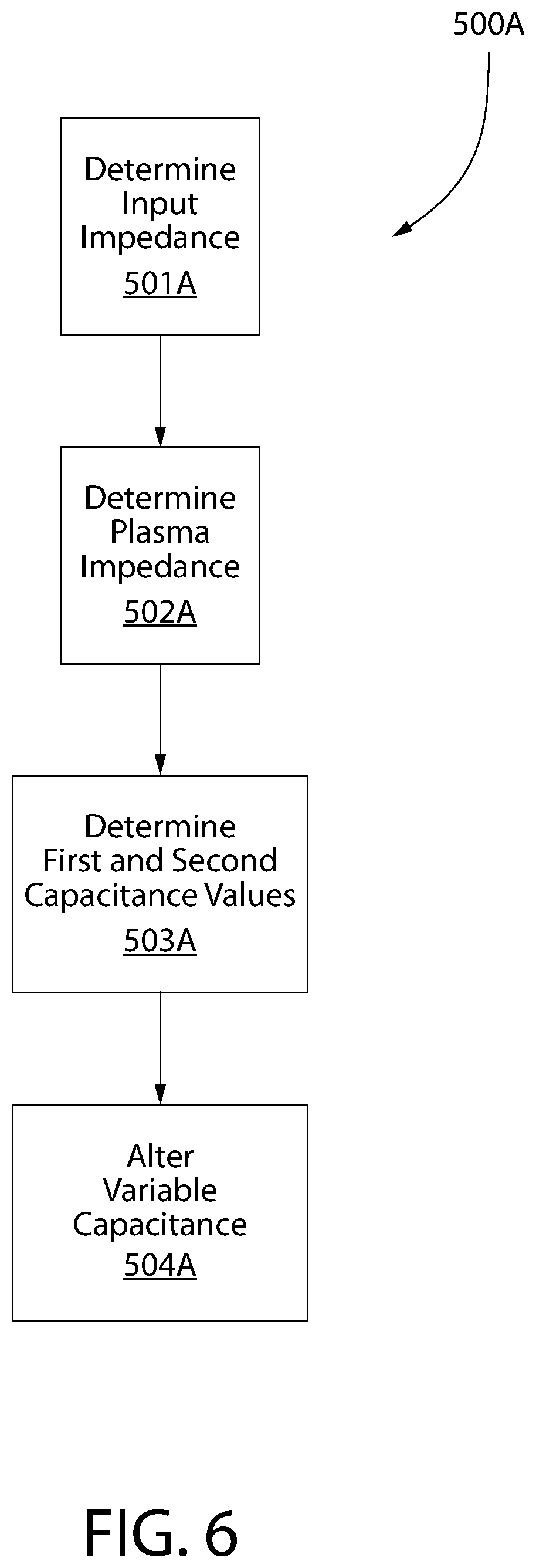
FIG. 6 is a flow chart showing a process 500A for matching an impedance according to one embodiment. The matching network can include components similar to those discussed above. In one embodiment, the matching network of FIG. 2 is utilized. In the first step of the exemplified process 500A of FIG. 6, an input impedance at the RF input 13 is determined (step 501A). The input impedance is based on the RF input parameter detected by the RF input sensor 21 at the RF input 13. The RF input sensor 21 can be any sensor configured to detect an RF input parameter at the RF input 13. The input parameter can be any parameter measurable at the RF input 13, including a voltage, a current, or a phase at the RF input 13. In the exemplified embodiment, the RF input sensor 21 detects the voltage, current, and phase at the RF input 13 of the matching network 11. Based on the RF input parameter detected by the RF input sensor 21, the control circuit 45 determines the input impedance.
Next, the control circuit 45 determines the plasma impedance presented by the plasma chamber 19 (step 502A). In one embodiment, the plasma impedance determination is based on the input impedance (determined in step 501A), the capacitance of the series EVC 31, and the capacitance of the shunt EVC 33. In other embodiments, the plasma impedance determination can be made using the output sensor 49 operably coupled to the RF output, the RF output sensor 49 configured to detect an RF output parameter. The RF output parameter can be any parameter measurable at the RF output 17, including a voltage, a current, or a phase at the RF output 17. The RF output sensor 49 may detect the output parameter at the RF output 17 of the matching network 11. Based on the RF output parameter detected by the RF output sensor 21, the control circuit 45 may determine the plasma impedance. In yet other embodiments, the plasma impedance determination can be based on both the RF output parameter and the RF input parameter.
Once the variable impedance of the plasma chamber 19 is known, the control circuit 45 can determine the changes to make to the variable capacitances of one or both of the series and shunt EVCs 31, 33 for purposes of achieving an impedance match. Specifically, the control circuit 45 determines a first capacitance value for the series variable capacitance and a second capacitance value for the shunt variable capacitance (step 503A). These values represent the new capacitance values for the series EVC 31 and shunt EVC 33 to enable an impedance match, or at least a substantial impedance match. In the exemplified embodiment, the determination of the first and second capacitance values is based on the variable plasma impedance (determined in step 502A) and the fixed RF source impedance.
Once the first and second capacitance values are determined, the control circuit 45 generates a control signal to alter at least one of the series variable capacitance and the shunt variable capacitance to the first capacitance value and the second capacitance value, respectively (step 504A). This is done at approximately t=-5 .mu.sec. The control signal instructs the switching circuit to alter the variable capacitance of one or both of the series and shunt EVCs 31, 33.
This alteration of the EVCs 31, 33 takes about 9-11 .mu.sec total, as compared to about 1-2 sec of time for an RF matching network using VVCs. Once the switch to the different variable capacitances is complete, there is a period of latency as the additional discrete capacitors that make up the EVCs join the circuit and charge. This part of the match tune process takes about 55 .mu.sec. Finally, the RF power profile 403 is shown decreasing, at just before t=56 .mu.sec, from about 380 mV peak-to-peak to about 100 mV peak-to-peak. This decrease in the RF power profile 403 represents the decrease in the reflected power 407, and it takes place over a time period of about 10 .mu.sec, at which point the match tune process is considered complete.
The altering of the series variable capacitance and the shunt variable capacitance can comprise sending a control signal to the series driver circuit 39 and the shunt driver circuit 43 to control the series variable capacitance and the shunt variable capacitance, respectively, where the series driver circuit 39 is operatively coupled to the series EVC 31, and the shunt driver circuit 43 is operatively coupled to the shunt EVC 43. When the EVCs 31, 33 are switched to their desired capacitance values, the input impedance may match the fixed RF source impedance (e.g., 50 Ohms), thus resulting in an impedance match. If, due to fluctuations in the plasma impedance, a sufficient impedance match does not result, the process of 500 A may be repeated one or more times to achieve an impedance match, or at least a substantial impedance match.
Using an RF matching network 11, such as that shown in FIG. 2, the input impedance can be represented as follows:
.times. ##EQU00001##
where Z.sub.in is the input impedance, Z.sub.P is the plasma impedance, Z.sub.L is the series inductor impedance, Z.sub.series is the series EVC impedance, and Z.sub.shunt is the shunt EVC impedance. In the exemplified embodiment, the input impedance (Z.sub.in) is determined using the RF input sensor 21. The EVC impedances (Z.sub.series and Z.sub.shunt) are known at any given time by the control circuitry, since the control circuitry is used to command the various discrete capacitors of each of the series and shunt EVCs to turn ON or OFF. Further, the series inductor impedance (Z.sub.L) is a fixed value. Thus, the system can use these values to solve for the plasma impedance (Z.sub.P).
Based on this determined plasma impedance (Z.sub.P) and the known desired input impedance (Z.sub.in') (which is typically 50 Ohms), and the known series inductor impedance (Z.sub.L), the system can determine a new series EVC impedance (Z.sub.series') and shunt EVC impedance (Z.sub.shunt').
''.times.''' ##EQU00002##
Based on the newly calculated series EVC variable impedance (Z.sub.series') and shunt EVC variable impedance (Z.sub.shunt'), the system can then determine the new capacitance value (first capacitance value) for the series variable capacitance and a new capacitance value (second capacitance value) for the shunt variable capacitance. When these new capacitance values are used with the series EVC 31 and the shunt EVC 33, respectively, an impedance match may be accomplished.
The exemplified method of computing the desired first and second capacitance values and reaching those values in one step is significantly faster than moving the two EVCs step-by-step to bring either the error signals to zero, or to bring the reflected power/reflection coefficient to a minimum. In semiconductor plasma processing, where a faster tuning scheme is desired, this approach provides a significant improvement in matching network tune speed.
Determining Capacitance Values Using Parameter Matrix
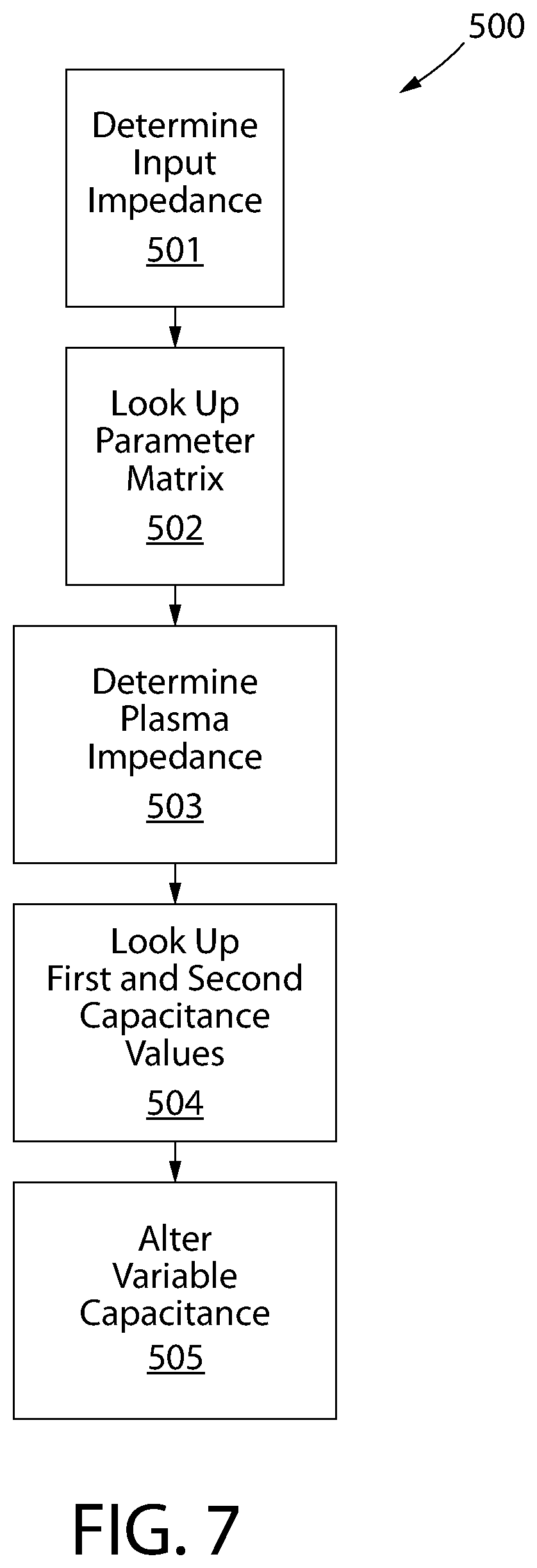
FIG. 7 provides an alternative process 500 for matching an impedance that uses a parameter matrix. In the exemplified process, the control circuit 45 (see FIG. 2 for matching network components) is configured and/or programmed to carry out each of the steps. As one of two initial steps, RF parameters are measured at the RF input 13 by the RF input sensor 21, and the input impedance at the RF input 13 is calculated (step 501) using the measured RF parameters. For this exemplified process 500, the forward voltage and the forward current are measured at the RF input 13. In certain other embodiments, the RF parameters may be measured at the RF output 17 by the RF output sensor 49, although in such embodiments, different calculations may be required than those described below. In still other embodiments, RF parameters may be measured at both the RF input 13 and the RF output 17.
The impedance matching circuit, coupled between the RF source 15 and the plasma chamber 19, may be characterized by one of several types of parameter matrices known to those of skill in the art. An S-parameter matrix and a Z-parameter matrix are two examples of such parameter matrices. Other examples include, but are not limited to, a Y-parameter matrix, a G-parameter matrix, an H-parameter matrix, a T-parameter matrix, and an ABCD-parameter matrix. Those of skill in the art will recognize also that these various parameter matrices may be mathematically converted from one to the other for an electrical circuit such as a matching network. The second initial step of the exemplified process 500 is to look up (step 502) the parameter matrix for the existing configuration of the impedance matching circuit in a parameter look-up table. The existing configuration of the impedance matching circuit is defined by existing operational parameters of the impedance matching circuit, particularly the existing array configurations for both of the series EVC 31 and the shunt EVC 33. In order to achieve an impedance match, the existing configuration of the impedance matching circuit is altered to a new configuration of the impedance matching circuit as part of the exemplified process 500.
The parameter look-up table includes a plurality of parameter matrices, with each parameter matrix being associated with a particular configuration of the series EVC 31 and the shunt EVC 33. The parameter look-up table may include one or more of the aforementioned types of parameter matrices. In the exemplified process 500, the parameter look-up table includes at least a plurality of S-parameter matrices. In certain embodiments, the parameter look-up table may include at least a plurality of Z-parameter matrices. In embodiments in which the parameter look-up table includes multiple types of parameter matrices, the different types of parameter matrices are associated within the parameter look-up table in such a way so as to eliminate the need for mathematical conversions between the different types of parameter matrices. For example, the T-parameter matrix may be included as part of the parameter look-up table, with each T-parameter matrix associated with the associated S-parameter matrix that would result from conversion between the two matrices.
The input impedance calculation (step 501) and the parameter matrix look up (step 502) may be performed in any order. With the input impedance calculated (step 501) and the parameter matrix for the existing configuration of the impedance matching circuit identified within the parameter look-up table (step 502) done, the plasma or load impedance may then be calculated (step 503) using the calculated input impedance and the parameter matrix for the existing configuration. Next, from the calculated plasma impedance, the match configurations for the series EVC 31 and the shunt EVC 33 that would achieve an impedance match, or at least a substantial impedance match, between the RF source 15 and the plasma chamber 19 are looked up (step 504) in an array configuration look-up table. These match configurations from the array configuration look-up table are the array configurations which will result in new capacitance values for the series EVC 31 and shunt EVC 33, with an impedance match being achieved with the new array configurations and associated new capacitance values. The array configuration look-up table is a table of array configurations for the series EVC 31 and the shunt EVC 33, and it includes each possible array configuration of the series EVC 31 and the shunt EVC 33 when used in combination. As an alternative to using an array configuration look-up table, the actual capacitance values for the EVCs 31, 33 may be calculated during the process--however, such real-time calculations of the capacitance values are inherently slower than looking up the match configurations in the array configuration look-up table. After the match configurations for the series EVC 31 and the shunt EVC 33 are identified in the array configuration look-up table, then one or both of the series array configuration and the shunt array configuration are altered (step 505) to the respective identified match configurations for the series EVC 31 and the shunt EVC 33.
The altering (step 505) of the series array configuration and the shunt array configuration may include the control circuit 45 sending a control signal to the series driver circuit 39 and the shunt driver circuit 43 to control the series array configuration and the shunt array configuration, respectively, where the series driver circuit 39 is operatively coupled to the series EVC 31, and the shunt driver circuit 43 is operatively coupled to the shunt EVC 43. When the EVCs 31, 33 are switched to the match configurations, the input impedance may match the fixed RF source impedance (e.g., 50 Ohms), thus resulting in an impedance match. If, due to fluctuations in the plasma impedance, a sufficient impedance match does not result, the process of 500 may be repeated one or more times to achieve an impedance match, or at least a substantial impedance match.
The look-up tables used in the process described above are compiled in advance of the RF matching network being used in conjunction with the plasma chamber 19. In creating the look-up tables, the RF matching network 11 is tested to determine at least one parameter matrix of each type and the load impedance associated with each array configuration of the series EVC 31 and the shunt EVC 33 prior to use with a plasma chamber. The parameter matrices resulting from the testing are compiled into the parameter look-up table so that at least one parameter matrix of each type is associated with a respective array configuration of the EVCs 31, 33. Similarly, the load impedances are compiled into the array configuration look-up table so that each parameter matrix is associated with a respective array configuration of the EVCs 31, 33. The pre-compiled look-up tables may take into consideration the fixed RF source impedance (e.g., 50 Ohms), the power output of the RF source, and the operational frequency of the RF source, among other factors that are relevant to the operation of the RF matching network. Each look-up table may therefore have tens of thousands of entries, or more, to account for all the possible configurations of the EVCs 31, 33. The number of possible configurations is primarily determined by how many discrete capacitors make up each of the EVCs 31, 33. In compiling the look-up tables, consideration may be given to possible safety limitations, such as maximum allowed voltages and currents at critical locations inside the matching network, and this may serve to exclude entries in one or more of the look-up tables for certain configurations of the EVCs 31, 33.
As is known in the art, the S-parameter matrix is composed of components called scatter parameters, or S-parameters for short. An S-parameter matrix for the impedance matching circuit has four S-parameters, namely S.sub.11, S.sub.12, S.sub.21, and S.sub.22, each of which represents a ratio of voltages at the RF input 13 and the RF output 17. All four of the S-parameters for the impedance matching circuit are determined and/or calculated in advance, so that the full S-parameter matrix is known. The parameters of the other types of parameter matrices may be similarly determined and/or calculated in advance and incorporated into the parameter matrix. For example, a Z-parameter matrix for the impedance matching circuit has four Z-parameters, namely Z.sub.11, Z.sub.12, Z.sub.21, and Z.sub.22.
By compiling the parameter look-up table in this manner, the entire time cost of certain calculations occurs during the testing phase for the RF matching network, and not during actual use of the RF matching network 11 with a plasma chamber 19. Moreover, because locating a value in a look-up table can take less time than calculating that same value in real time, using the look-up table can aid in reducing the overall time needed to achieve an impedance match. In a plasma deposition or etching process which includes potentially hundreds or thousands of impedance matching adjustments throughout the process, this time savings can help add directly to cost savings for the overall fabrication process.
From the beginning of the match tune process, which starts with the control circuit determining the variable impedance of the plasma chamber and determining the series and shunt match configurations, to the end of the match tune process, when the RF power reflected back toward the RF source decreases, the entire match tune process of the RF impedance matching network using EVCs has an elapsed time of approximately 110 .mu.sec, or on the order of about 150 .mu.sec or less. This short elapsed time period for a single iteration of the match tune process represents a significant increase over a VVC matching network. Moreover, because of this short elapsed time period for a single iteration of the match tune process, the RF impedance matching network using EVCs may iteratively perform the match tune process, repeating the two determining steps and the generating another control signal for further alterations to the array configurations of one or both of the electronically variable capacitors. By iteratively repeating the match tune process, it is anticipated that a better impedance match may be created within about 2-4 iterations of the match tune process. Moreover, depending upon the time it takes for each repetition of the match tune process, it is anticipated that 3-4 iterations may be performed in 500 .mu.sec or less. Given the 1-2 sec match time for a single iteration of a match tune process for RF impedance matching networks using VVCs, this ability to perform multiple iterations in a fraction of the time represents a significant advantage for RF impedance matching networks using EVCs.
Those of skill in the art will recognize that several factors may contribute to the sub-millisecond elapsed time of the impedance matching process for an RF impedance matching network using EVCs. Such factors may include the power of the RF signal, the configuration and design of the EVCs, the type of matching network being used, and the type and configuration of the driver circuit being used. Other factors not listed may also contribute to the overall elapsed time of the impedance matching process. Thus, it is expected that the entire match tune process for an RF impedance matching network having EVCs should take no more than about 500 .mu.sec to complete from the beginning of the process (i.e., measuring by the control circuit and calculating adjustments needed to create the impedance match) to the end of the process (the point in time when the efficiency of RF power coupled into the plasma chamber is increased due to an impedance match and a reduction of the reflected power). Even at a match tune process on the order of 500 .mu.sec, this process time still represents a significant improvement over RF impedance matching networks using VVCs.
Table 1 presents data showing a comparison between operational parameters of one example of an EVC versus one example of a VVC. As can be seen, EVCs present several advantages, in addition to enabling fast switching for an RF impedance matching network:
TABLE-US-00001 TABLE 1 Typical 1000 pF Parameter EVC Vacuum Capacitors Capacitance 20 pF~1400 pF 15 pF~1000 pF Reliability High Low Response Time ~500 .mu.sec 1 s~2 s ESR ~13 mW ~20 mW Voltage 7 kV 5 kV Current Handling Capability 216 A rms 80 A rms Volume 4.5 in.sup.3 75 in.sup.3
As is seen, in addition to the fast switching capabilities made possible by the EVC, EVCs also introduce a reliability advantage, a current handling advantage, and a size advantage. Additional advantages of the RF impedance matching network using EVCs and/or the switching circuit itself for the EVCs include: The disclosed RF impedance matching network does not include any moving parts, so the likelihood of a mechanical failure reduced to that of other entirely electrical circuits which may be used as part of the semiconductor fabrication process. For example, the typical EVC may be formed from a rugged ceramic substrate with copper metallization to form the discrete capacitors. The elimination of moving parts also increases the resistance to breakdown due to thermal fluctuations during use. The EVC has a compact size as compared to a VVC, so that the reduced weight and volume may save valuable space within a fabrication facility. The design of the EVC introduces an increased ability to customize the RF matching network for specific design needs of a particular application. EVCs may be configured with custom capacitance ranges, one example of which is a non-linear capacitance range. Such custom capacitance ranges can provide better impedance matching for a wider range of processes. As another example, a custom capacitance range may provide more resolution in certain areas of impedance matching. A custom capacitance range may also enable generation of higher ignition voltages for easier plasma strikes. The short match tune process (.about.500 .mu.sec or less) allows the RF impedance matching network to better keep up with plasma changes within the fabrication process, thereby increasing plasma stability and resulting in more controlled power to the fabrication process. The use of EVCs, which are digitally controlled, non-mechanical devices, in an RF impedance matching network provides greater opportunity to fine tune control algorithms through programming. EVCs exhibit superior low frequency (kHz) performance as compared to VVCs. Altering Frequency of RF Source to Fine Tune Match
FIG. 8 is a flow chart showing a process 600 for matching an impedance according to another embodiment. Since EVCs can provide only discretized capacitance values, a matching network that varies only EVCs to create an impedance match can only match based on these discretized values. For example, if a plasma impedance occurs such that the series and/or shunt capacitance values needed to bring the input impedance of the matching network to a desired non-reactive 50 Ohms lies in-between the discretized values, the EVC-based matching network will not be able to tune the input impedance of the matching network to the non-reactive 50 Ohms. The process 600 of FIG. 8 addresses such a circumstance by also altering a frequency of the RF source (sometimes referred to as the "RF generator") to carry out the impedance match.
The RF source, matching network, and plasma chamber of process 600 can be configured similarly to the system of FIG. 2. Accordingly, reference will be made to the components of the system of FIG. 2, though this figure represents just one embodiment of the invention.
As with previously discussed embodiments, the matching network 11 of process 600 can include an RF input 13 configured to receive an RF signal from an RF source 15, and an RF output 17 configured to operably couple to a plasma chamber 19. The matching network can further include at least one EVC 31, 33, and a control circuit 45 for instructing the at least one EVC 31, 33 to alter its variable capacitance. The RF source 15 (including its control circuitry) and the RF matching network 11 can be in the same enclosure or separate enclosures.
In the process 600, the matching network 11 is initially in an auto tuning mode (step 601). In this mode, the matching network 11 can be configured to carry out automated tuning by altering at least one capacitance value in a manner similar to that described in the foregoing embodiments. In this mode, the process 600 performs tuning referred to as primary tuning (step 602). In the exemplified embodiment, the primary tuning includes altering the series and/or shunt capacitance values in an attempt to achieve an impedance match. In the exemplified embodiment, the desired input impedance (the desired impedance at the input of the matching network 11) is a fixed, non-reactive 50 Ohm, sometimes referred to as the RF source impedance. In other embodiments, the desired input impedance can be any other impedance value, and can be variable.
In the exemplified embodiment, the primary tuning will bring the input impedance relatively close to a non-reactive 50 Ohms, the matching network 11 being limited by the discretized capacitance values of the EVCs 31, 33. At this stage, a preliminary match is achieved (step 603). The preliminary match state will have an associated first reflection parameter value at the RF source output 15a (the RF source output 15a being connected to the matching network input 13). In the exemplified embodiment, the first reflection parameter value is a reflected power value. In other embodiments, the first reflection parameter value can be any reflection-related parameter associated with the preliminary match state. For example, the first reflection parameter value can be the reflection coefficient, which represents the ratio of the amplitude of the reflected wave to the incident wave, and is sometimes referred to as gamma. The first reflection parameter can be measured by sensor 21 at the RF source output 15a. In other embodiments, reflected power can be measured by a sensor or comparable device that is located proximate to the matching network input 13.
In one embodiment, the alteration of variable capacitance in auto tuning mode can include the steps of adjusting the variable capacitance, determining an intermediate reflection parameter value, and then reducing and/or increasing the variable capacitance based on the intermediate reflection parameter value. This process can be repeated such that there are several intermediate reflection parameter values, the adjustment of the one or more variable capacitances being based on these intermediate reflection parameter values. In other embodiments, the invention can omit the use of intermediate reflection parameter values.
Once the preliminary match state is achieved, the matching network 11 can provide a control signal to the RF source 15 indicating that primary tuning is complete and that a preliminary match has been achieved (step 604). The control signal can be any signal sufficient to provide indication that the preliminary match has been achieved.
In response, the RF source 15 can send a hold signal to the matching network 11 (step 605), the hold signal placing the matching network 11 in a manual tuning mode (step 606). In manual tuning mode, the matching network 11 will stop performing automated tuning (and therefore will not alter the variable capacitances) as long as the hold signal is present. In other embodiments, the matching network 11 can automatically enter manual tuning mode when the preliminary match has been achieved, and can return to auto tuning mode when receiving an instruction from the RF source 15.
Next, the variable frequency of the RF source 15 can be adjusted to perform secondary tuning (step 607). This secondary tuning can fine tune the input impedance of the matching network 1 to the desired non-reactive 50 Ohm, or other desired impedance, and can minimize the reflected power at the output of the RF source 15, thereby also decreasing the reflection coefficient. The RF source 15 can have standard control circuitry by which the frequency is varied and the signals discussed above are sent, received, and processed. The frequency can be altered by providing a command to a frequency generation circuit that forms part of the RF source, such as a Direct Digital Synthesizer.
Once the RF source 15 has completed altering the frequency for the secondary tuning, a final match state is achieved (step 608). The final match state will have an associated second reflection parameter value at the RF source output 15a. As with the first reflection parameter value, in the exemplified embodiment, the second reflection parameter value is a reflected power value. In other embodiments, the second reflection parameter value can be any reflection-related parameter associated with the preliminary match state, such as the reflection coefficient (discussed above). The second reflection parameter can be measured by a sensor 21 at the RF source output 15a. Since the final match state causes a more finely tuned match than the preliminary match state, the second reflection parameter value will be less than the first reflection parameter value.
The alteration of the variable RF source frequency can include reducing and/or increasing the variable RF source frequency based on an intermediate reflection parameter value. In one embodiment, the alteration of the variable source frequency includes reducing the variable RF source frequency by a first amount and determining the intermediate reflection parameter value at the RF source output. If the intermediate reflection parameter value decreases, the variable RF source frequency is again reduced by the first amount and a new intermediate reflection parameter value is measured. This process can repeat until the intermediate reflection parameter value increases. When the intermediate reflection parameter value increases, the variable source frequency can be increased by a second amount (the second amount being less than the first amount), and then a new intermediate reflection parameter value is determined. If the new intermediate reflection parameter value decreases, the variable source frequency is again increased by the second amount, and a new intermediate reflection parameter value is determined. This process can repeat until the new intermediate reflection parameter value increases or is zero, at which stage the process can stop or the variable source frequency can be returned to its previous value.
The invention is not limited to any one embodiment for tuning the frequency or variable capacitance. For example, the invention can use any variety of methods to step up and/or down the frequency in different increments based on the resulting reflected power. Further, the process 600 can have a minimum reflected parameter value (e.g., a minimum reflected power or minimum reflection coefficient). When the minimum reflected parameter value is achieved, the tuning can stop, regardless of whether the process is in primary or secondary tuning.
Returning to the exemplified embodiment, once the final match state is achieved, the RF source 15 can send a signal (sometimes referred to as a "resume signal") to the matching network 11 to place the matching network 11 back into auto tuning mode (step 609). The matching network 11 can then be ready for the next variation of the plasma impedance. Thus, when a plasma impedance of the plasma chamber 15 changes, the control circuit 45 can repeat the instruction to alter the variable capacitance and/or the instruction to alter the variable RF source frequency.
In other embodiments, the process 600 will not resume tuning until the reflection parameter value exceeds a predetermined value. Such a tuning restart threshold can be applied to the primary tuning, the secondary tuning, or both. Further, thresholds can be set such that, for small reflected power level raises, only secondary tuning is done (altering the RF source frequency), while, for larger reflected power levels, primary tuning is first carried out (altering capacitances), followed by secondary tuning (altering the RF source frequency).
Combining an EVC-based RF matching network with a variable frequency RF source provides several advantages for fast and precise RF matching. For example, with all components being electronic, the system has higher reliability than those using VVC technology, which are prone to mechanical failures. Further, the primary and second tuning can be performed quickly to enable matching within 500 .mu.sec. Further, the combined EVC matching network and variable RF source can decrease the reflected power to the RF source to essentially 0 Watts.
Restricted Capacitor Switching
The matching networks discussed above can alter their variable capacitance values to achieve an impedance match. This process is sometimes referred to as tuning. The state of the impedance matching can be assessed based on a reflection parameter value. In the exemplified embodiments, the reflection parameter value is a reflected power value. More specifically, the reflection parameter value is a reflection coefficient value (sometimes referred to as "gamma"), which represents the ratio of the amplitude of a reflected wave to an incident wave. Referring to the system 85 of FIG. 2, a reflection parameter value can be measured by sensor 21 at the matching network input 13 (or RF source 15 output), or by sensor 49 at the matching network output 17 (or plasma chamber 19 input). Such a sensor can provide a signal to the control circuit 45 indicative of the reflection parameter value.
In other embodiments, the reflection parameter value can be any reflection-related parameter associated with a match state. For example, the reflection parameter value can be a load impedance at the RF output, since a changing load impedance will alter the reflected power of the system. In one embodiment, this load impedance can be directly measured using a sensor at the RF output of the matching network. In other embodiments, the load impedance can be calculated based on other parameters (as discussed above). For example, the matching network can determine the input impedance using a sensor (such as a VI sensor) at the RF input of the matching network, and then use this measured input impedance and the current EVC switch positions to calculate the load impedance. This process of calculating the load impedance can include use of a look-up table as discussed above.
In one approach to achieving an impedance match, a matching algorithm requires the control loop of the RF matching network to continue to tune until the reflection coefficient value at the input of the matching network is reduced below a certain level. This level is sometimes referred to as "gamma-stop." If the load impedance changes, the reflection coefficient at the input of the RF matching network can increase. If this reflection coefficient increases beyond a certain reflection coefficient value, sometimes referred to as "gamma-restart," then the RF matching network starts to tune again. In a solid-state RF matching network, there are typically no restrictions on how many switches can switch ON or OFF at any time, therefore based on the change in the reflection coefficient, the number of switches switching at any time can be significant and thus can result in perturbing the plasma to make it unstable.
In an alternative approach, an intermediate gamma value is utilized such that there are three gamma values: (1) a first reflection value (gamma-stop) at which tuning is stopped, (2) a second reflection value (gamma-restart-low) at which capacitor switching is limited, and (3) a third reflection value (gamma-restart-high) at which capacitor switching is unlimited. This alternative approach is described below.
FIG. 9 is flow chart showing a process for matching an impedance where capacitor switching can be restricted using the above three reflection values. In the exemplified embodiment, the reflection coefficient value is continuously monitored (operation 202). When the match is tuned and the reflection coefficient value (gamma) is not above the first reflection value (operation 204), no capacitors switch (operation 210). When the reflection coefficient value goes above the second reflection value (but is at or below the third reflection value) (operation 206), only a predetermined number of predetermined fine capacitors can switch at this time (restricted tune) (operation 212). Whether to turn these switches ON or OFF will depend upon what was the actual calculated position of the capacitors. When the reflection coefficient value goes above the third reflection value (operation 208), the capacitors can switch without any restrictions (unrestricted tune) (operation 214). For the purpose of this description, the fine capacitors can be any capacitors that are used to provide finer capacitance movement steps than the coarse capacitors. In one embodiment, the coarse capacitors have a capacitance at least twice as large as the capacitance of the fine capacitors.
In one example, the predetermined number is two (only two capacitors can switch when the reflection coefficient value initially exceeds the second reflection value), and the three reflection values are as follows: (1) first reflection value (gamma-stop)=0.031, (2) second reflection value (gamma-restart-low)=0.07, (3) third reflection value (gamma-restart-high)=0.10. In this example, the matched position is C4F5/C6F7 (i.e., 4 coarse capacitor switch ON and 5 fine capacitor switch ON for one solid state capacitor array, and 6 coarse capacitor switch ON and 7 fine capacitor switch ON for the second solid state capacitor array), and this positioning is determined before determining how to switch the discrete capacitors.
If the reflection coefficient value is calculated as 0.08, and the new tuned position is calculated to be C3F0/C7F1, then the match will go to C4F3/C6F9, rather than going directly to C3F0/C7F1. The control circuit can continuously monitor the reflection coefficient value (or other reflection parameter), and thus this loop can run as many times as needed until either the reflection coefficient value goes below the first reflection value or the reflection coefficient value goes above the third reflection value. If the reflection coefficient value goes above the third reflection value (i.e., 0.10), then the capacitor switches are not restricted and can directly switch to the calculated position. Note that the foregoing capacitor restrictions can also be applied to when the match is moving from a higher reflection coefficient value to a lower reflection coefficient value to provide a slower settling profile. Not also, while the embodiment described above discusses altering the tuning based on whether a reflection parameter is above, or at, or below a reflection parameter (or some combination thereof), other embodiments can use any one of these options (or a combination of options) provided different values are used as reference values for determining what type of tuning to use. For example, in one embodiment the system can carry out an unrestricted tune when the reflection parameter is above the third reflection value, while in another embodiment the system can carry out an unrestricted tune when the reflection parameter is at or above the third reflection value.
By the above multi-step reflection value approach, if something changes in the process that changes the impedance by a significant amount, then the match can respond faster, but if the change is small, then the match will not take big steps to cause the plasma to become unstable. This restricted capacitor switching approach can be used, for example, with the matching networks discussed above. A control circuit, such as control circuit 45 or 645 can be used to carry out the steps of determining or receiving the reflection parameter value and controlling the altering of the discrete capacitors based on that value. It is further noted that the restricted capacitor approach described above can be used in conjunction with the other impedance matching and capacitor-switching methods discussed herein. Further, the restricted capacitor switching approach can be used with a matching network that forms part of a semiconductor processing tool, such as that shown in FIGS. 1-3. Further, the restricted capacitor switching approach can be used with a matching network as part of a method of manufacturing a semiconductor.
While the embodiments of a matching network discussed herein have used L or pi configurations, it is noted that he claimed matching network may be configured in other matching network configurations, such as a `T` type configuration. Unless stated otherwise, the variable capacitors, switching circuits, and methods discussed herein may be used with any configuration appropriate for an RF impedance matching network.
While the embodiments discussed herein use one or more variable capacitors in a matching network to achieve an impedance match, it is noted that any variable reactance element can be used. A variable reactance element can include one or more discrete reactance elements, where a reactance element is a capacitor or inductor or similar reactive device.
While the inventions have been described with respect to specific examples including presently preferred modes of carrying out the invention, those skilled in the art will appreciate that there are numerous variations and permutations of the above described systems and techniques. It is to be understood that other embodiments may be utilized and structural and functional modifications may be made without departing from the scope of the present inventions. Thus, the spirit and scope of the inventions should be construed broadly as set forth in the appended claims.
* * * * *
D00000
D00001
D00002
D00003
D00004
D00005
D00006
D00007
D00008
D00009
M00001
M00002
XML
uspto.report is an independent third-party trademark research tool that is not affiliated, endorsed, or sponsored by the United States Patent and Trademark Office (USPTO) or any other governmental organization. The information provided by uspto.report is based on publicly available data at the time of writing and is intended for informational purposes only.
While we strive to provide accurate and up-to-date information, we do not guarantee the accuracy, completeness, reliability, or suitability of the information displayed on this site. The use of this site is at your own risk. Any reliance you place on such information is therefore strictly at your own risk.
All official trademark data, including owner information, should be verified by visiting the official USPTO website at www.uspto.gov. This site is not intended to replace professional legal advice and should not be used as a substitute for consulting with a legal professional who is knowledgeable about trademark law.