Routing assembly and system using same
Lloyd , et al. Sept
U.S. patent number 10,424,856 [Application Number 15/561,852] was granted by the patent office on 2019-09-24 for routing assembly and system using same. This patent grant is currently assigned to Molex, LLC. The grantee listed for this patent is Molex, LLC. Invention is credited to Gregory Fitzgerald, Ayman Isaac, Brian Keith Lloyd, Bruce Reed, Gregory Walz.


View All Diagrams
| United States Patent | 10,424,856 |
| Lloyd , et al. | September 24, 2019 |
Routing assembly and system using same
Abstract
A routing assembly for an electronic device has a front face with an array of connectors ports and each of the connector ports contain a first connector mounted therein. A first end of a cable can be directly terminated to the first connectors and the cables can be embedded in a tray that is configured to extend toward a chip package. The cables extend from the tray and terminates to a second connector that can be connected to the chip package so as to provide a communication path between the first connector and the second connector that bypasses any supporting circuit board.
| Inventors: | Lloyd; Brian Keith (Maumelle, AR), Fitzgerald; Gregory (Merrimack, NH), Reed; Bruce (Maumelle, AR), Walz; Gregory (Maumelle, AR), Isaac; Ayman (Little Rock, AR) | ||||||||||
|---|---|---|---|---|---|---|---|---|---|---|---|
| Applicant: |
|
||||||||||
| Assignee: | Molex, LLC (Lisle, IL) |
||||||||||
| Family ID: | 59312135 | ||||||||||
| Appl. No.: | 15/561,852 | ||||||||||
| Filed: | January 11, 2017 | ||||||||||
| PCT Filed: | January 11, 2017 | ||||||||||
| PCT No.: | PCT/US2017/012917 | ||||||||||
| 371(c)(1),(2),(4) Date: | September 26, 2017 | ||||||||||
| PCT Pub. No.: | WO2017/123574 | ||||||||||
| PCT Pub. Date: | July 20, 2017 |
Prior Publication Data
| Document Identifier | Publication Date | |
|---|---|---|
| US 20180309214 A1 | Oct 25, 2018 | |
Related U.S. Patent Documents
| Application Number | Filing Date | Patent Number | Issue Date | ||
|---|---|---|---|---|---|
| 62277275 | Jan 11, 2016 | ||||
| Current U.S. Class: | 1/1 |
| Current CPC Class: | H01R 12/73 (20130101); H01R 12/79 (20130101); H01R 12/7076 (20130101); H01R 13/518 (20130101); G06F 13/38 (20130101); H01L 2924/15192 (20130101) |
| Current International Class: | G06F 13/38 (20060101); H01R 12/73 (20110101); H01R 12/79 (20110101); H01R 12/70 (20110101); H01R 13/518 (20060101) |
| Field of Search: | ;439/492,494,502 ;333/33,34,260,238,246 |
References Cited [Referenced By]
U.S. Patent Documents
| 3007131 | October 1961 | Dahlgren et al. |
| 3594613 | July 1971 | Prietula |
| 3963319 | June 1976 | Schumacher |
| 4025141 | May 1977 | Thelissen |
| 4072387 | February 1978 | Sochor |
| 4083615 | April 1978 | Volinskie |
| 4157612 | June 1979 | Rainal |
| 4290664 | September 1981 | Davis |
| 4307926 | December 1981 | Smith |
| 4346355 | August 1982 | Tsukii |
| 4417779 | November 1983 | Wilson |
| 4508403 | April 1985 | Weltman |
| 4611186 | September 1986 | Ziegner |
| 4615578 | October 1986 | Stadler |
| 4639054 | January 1987 | Kersbergen |
| 4656441 | April 1987 | Takahashi |
| 4657329 | April 1987 | Dechelette |
| 4679321 | July 1987 | Plonski |
| 4697862 | October 1987 | Hasircoglu |
| 4724409 | February 1988 | Lehman |
| 4889500 | December 1989 | Lazar |
| 4924179 | May 1990 | Sherman |
| 4948379 | August 1990 | Evans |
| 4984992 | January 1991 | Beamenderfer et al. |
| 4991001 | February 1991 | Takubo |
| 5112251 | May 1992 | Cesar |
| 5197893 | March 1993 | Morlion et al. |
| 5332979 | July 1994 | Roskewitsch |
| 5387130 | February 1995 | Fedder et al. |
| 5402088 | March 1995 | Pierro |
| 5435757 | July 1995 | Fedder et al. |
| 5441424 | August 1995 | Morlion et al. |
| 5487673 | January 1996 | Hurtarte |
| 5509827 | April 1996 | Huppenthal et al. |
| 5554038 | September 1996 | Morlion et al. |
| 5598627 | February 1997 | Saka et al. |
| 5632634 | May 1997 | Soes |
| 5691506 | November 1997 | Miyazaki et al. |
| 5781759 | July 1998 | Kashiwabara |
| 5876239 | March 1999 | Morin et al. |
| 6004139 | December 1999 | Dramstad |
| 6053770 | April 2000 | Blom |
| 6083046 | July 2000 | Wu et al. |
| 6095872 | August 2000 | Lang et al. |
| 6144559 | November 2000 | Johnson et al. |
| 6156981 | December 2000 | Ward et al. |
| 6203376 | March 2001 | Magajne et al. |
| 6255741 | July 2001 | Yoshihara |
| 6266712 | July 2001 | Henrichs |
| 6273753 | August 2001 | Ko |
| 6273758 | August 2001 | Lloyd |
| 6366471 | April 2002 | Edwards et al. |
| 6368120 | April 2002 | Scherer |
| 6371788 | April 2002 | Bowling et al. |
| 6452789 | September 2002 | Pallotti et al. |
| 6489563 | December 2002 | Zhao et al. |
| 6535367 | March 2003 | Carpenter |
| 6574115 | June 2003 | Asano et al. |
| 6575772 | June 2003 | Soubh et al. |
| 6592401 | July 2003 | Gardner et al. |
| 6652296 | November 2003 | Kuroda et al. |
| 6652318 | November 2003 | Winings et al. |
| 6685501 | February 2004 | Wu et al. |
| 6692262 | February 2004 | Loveless |
| 6705893 | March 2004 | Ko |
| 6780069 | August 2004 | Scherer |
| 6797891 | September 2004 | Blair et al. |
| 6824426 | November 2004 | Spink, Jr. |
| 6843657 | January 2005 | Driscoll et al. |
| 6882241 | April 2005 | Abo |
| 6903934 | June 2005 | Lo |
| 6910914 | June 2005 | Spink, Jr. |
| 6916183 | July 2005 | Alger et al. |
| 6955565 | October 2005 | Lloyd |
| 6969270 | November 2005 | Renfro |
| 6969280 | November 2005 | Chien |
| 6971887 | December 2005 | Trobough |
| 7004765 | February 2006 | Hsu |
| 7004793 | February 2006 | Scherer |
| 7044772 | May 2006 | McCreery |
| 7052292 | May 2006 | Hsu et al. |
| 7056128 | June 2006 | Driscoll et al. |
| 7066756 | June 2006 | Lange et al. |
| 7070446 | July 2006 | Henry |
| 7108522 | September 2006 | Verelst et al. |
| 7148428 | December 2006 | Meier et al. |
| 7168961 | January 2007 | Hsieh |
| 7175446 | February 2007 | Bright |
| 7192300 | March 2007 | Hashiguchi et al. |
| 7214097 | May 2007 | Hsu et al. |
| 7223915 | May 2007 | Hackman |
| 7234944 | June 2007 | Nordin |
| 7244137 | July 2007 | Renfro et al. |
| 7280372 | October 2007 | Grundy et al. |
| 7307293 | December 2007 | Fjelstad et al. |
| 7331816 | February 2008 | Krohn et al. |
| 7384275 | June 2008 | Ngo |
| 7394665 | July 2008 | Hamasaki et al. |
| 7402048 | July 2008 | Meier et al. |
| 7431608 | October 2008 | Sakaguchi et al. |
| 7445471 | November 2008 | Scherer et al. |
| 7462924 | December 2008 | Shuey |
| 7489514 | February 2009 | Hamasaki |
| 7534142 | May 2009 | Avery |
| 7540773 | June 2009 | Ko |
| 7549897 | June 2009 | Fedder et al. |
| 7621779 | November 2009 | Laurx et al. |
| 7637767 | December 2009 | Davis |
| 7654831 | February 2010 | Wu |
| 7658654 | February 2010 | Ohyama |
| 7690930 | April 2010 | Chen et al. |
| 7719843 | May 2010 | Dunham |
| 7744385 | June 2010 | Scherer |
| 7744403 | June 2010 | Barr |
| 7744414 | June 2010 | Scherer et al. |
| 7748988 | July 2010 | Hori |
| 7771207 | August 2010 | Hamner et al. |
| 7789529 | September 2010 | Roberts |
| 7819675 | October 2010 | Ko et al. |
| 7824197 | November 2010 | Westman |
| 7857629 | December 2010 | Chin |
| 7857630 | December 2010 | Hermant et al. |
| 7862344 | January 2011 | Morgan |
| 7892019 | February 2011 | Rao |
| 7906730 | March 2011 | Atkinson et al. |
| 7931502 | April 2011 | Iida |
| 7985097 | July 2011 | Gulla |
| 7997933 | August 2011 | Feldman |
| 8002583 | August 2011 | van Woensel |
| 8018733 | September 2011 | Jia |
| 8036500 | October 2011 | McColloch |
| 8157573 | April 2012 | Tanaka |
| 8162675 | April 2012 | Regnier |
| 8187038 | May 2012 | Kamiya |
| 8192222 | June 2012 | Kameyama |
| 8226441 | July 2012 | Regnier |
| 8308491 | November 2012 | Nichols et al. |
| 8337243 | December 2012 | Elkhatib et al. |
| 8338713 | December 2012 | Fjelstad et al. |
| 8398433 | March 2013 | Yang |
| 8419472 | April 2013 | Swanger |
| 8435074 | May 2013 | Grant |
| 8439704 | May 2013 | Reed |
| 8449312 | May 2013 | Lang |
| 8449330 | May 2013 | Schroll |
| 8465302 | June 2013 | Regnier |
| 8480413 | July 2013 | Minich |
| 8517765 | August 2013 | Schroll |
| 8535069 | September 2013 | Zhang |
| 8540525 | September 2013 | Regnier |
| 8575529 | September 2013 | Asahi |
| 8553102 | October 2013 | Yamada |
| 8575491 | November 2013 | Gundel et al. |
| 8588561 | November 2013 | Zbinden |
| 8597055 | December 2013 | Regnier |
| 8651890 | February 2014 | Chiarelli |
| 8672707 | March 2014 | Nichols et al. |
| 8690604 | April 2014 | Davis |
| 8715003 | May 2014 | Buck |
| 8740644 | June 2014 | Long |
| 8747158 | June 2014 | Szczesny |
| 8753145 | June 2014 | Lang |
| 8758051 | June 2014 | Nonen et al. |
| 8764483 | July 2014 | Ellison |
| 8784122 | July 2014 | Soubh |
| 8787711 | July 2014 | Zbinden |
| 8794991 | August 2014 | Ngo |
| 8804342 | August 2014 | Behziz et al. |
| 8814595 | August 2014 | Cohen et al. |
| 8834190 | September 2014 | Ngo |
| 8864521 | October 2014 | Atkinson et al. |
| 8888533 | November 2014 | Westman et al. |
| 8905767 | December 2014 | Putt, Jr. et al. |
| 8911255 | December 2014 | Scherer et al. |
| 8926342 | January 2015 | Vinther |
| 8926377 | January 2015 | Kirk |
| 8992236 | March 2015 | Wittig |
| 8992237 | March 2015 | Regnier |
| 8992258 | March 2015 | Raschilla |
| 9011177 | April 2015 | Lloyd |
| 9028281 | May 2015 | Kirk |
| 9035183 | May 2015 | Kodama et al. |
| 9040824 | May 2015 | Guetig et al. |
| 9054432 | June 2015 | Yang |
| 9071001 | June 2015 | Scherer et al. |
| 9119292 | August 2015 | Gundel |
| 9136652 | September 2015 | Ngo |
| 9142921 | September 2015 | Wanha et al. |
| 9155214 | October 2015 | Ritter |
| 9160123 | October 2015 | Pao |
| 9160151 | October 2015 | Vinther |
| 9161463 | October 2015 | Takamura |
| 9166320 | October 2015 | Herring |
| 9196983 | November 2015 | Saur et al. |
| 9203171 | December 2015 | Yu |
| 9209539 | December 2015 | Herring |
| 9214756 | December 2015 | Nishio |
| 9214768 | December 2015 | Pao |
| 9232676 | January 2016 | Sechrist et al. |
| 9246251 | January 2016 | Regnier |
| 9277649 | March 2016 | Ellison |
| 9312618 | April 2016 | Regnier |
| 9331432 | May 2016 | Phillips |
| 9350108 | May 2016 | Long |
| 9356366 | May 2016 | Moore |
| 9385455 | July 2016 | Regnier |
| 9391407 | July 2016 | Bucher |
| 9401563 | July 2016 | Simpson |
| 9413090 | August 2016 | Nagamine |
| 9413112 | August 2016 | Helster |
| 9431773 | August 2016 | Chen |
| 9437981 | September 2016 | Wu |
| 9455538 | September 2016 | Nishio |
| 9484671 | November 2016 | Zhu |
| 9484673 | November 2016 | Yang |
| 9490587 | November 2016 | Phillips |
| 9496655 | November 2016 | Huang |
| 9515429 | December 2016 | DeGeest |
| 9525245 | December 2016 | Regnier |
| 9543688 | January 2017 | Pao |
| 9553381 | January 2017 | Regnier |
| 9559465 | January 2017 | Phillips |
| 9565780 | February 2017 | Nishio |
| 9608388 | March 2017 | Kondo |
| 9608590 | March 2017 | Hamner |
| 9627818 | April 2017 | Chen |
| 9660364 | May 2017 | Wig et al. |
| 9666998 | May 2017 | deBoer |
| 9673570 | June 2017 | Briant |
| 9812799 | November 2017 | Wittig |
| 9985367 | May 2018 | Wanha |
| 2001/0016438 | August 2001 | Reed |
| 2002/0111067 | August 2002 | Sakurai et al. |
| 2002/0157865 | October 2002 | Noda |
| 2002/0180554 | December 2002 | Clark |
| 2003/0064616 | April 2003 | Reed et al. |
| 2003/0073331 | April 2003 | Peloza et al. |
| 2003/0222282 | December 2003 | Fjelstad et al. |
| 2004/0094328 | May 2004 | Fjelstad et al. |
| 2004/0121633 | June 2004 | David et al. |
| 2004/0155328 | August 2004 | Kline |
| 2004/0155734 | August 2004 | Kosemura |
| 2004/0229510 | November 2004 | Lloyd |
| 2004/0264894 | December 2004 | Cooke |
| 2005/0006126 | January 2005 | Aisenbrey |
| 2005/0051810 | March 2005 | Funakura |
| 2005/0093127 | May 2005 | Fjelstad et al. |
| 2005/0130490 | June 2005 | Rose |
| 2005/0142944 | June 2005 | Ling et al. |
| 2005/0239339 | October 2005 | Pepe |
| 2006/0001163 | January 2006 | Kolbehdari et al. |
| 2006/0035523 | February 2006 | Kuroda et al. |
| 2006/0038287 | February 2006 | Hamasaki |
| 2006/0079102 | April 2006 | DeLessert |
| 2006/0079119 | April 2006 | Wu |
| 2006/0091507 | May 2006 | Fjelstad et al. |
| 2006/0114016 | June 2006 | Suzuki |
| 2006/0160399 | July 2006 | Dawiedczyk |
| 2006/0189212 | August 2006 | Avery |
| 2006/0194475 | August 2006 | Miyazaki |
| 2006/0216969 | September 2006 | Bright |
| 2006/0228922 | October 2006 | Morriss |
| 2006/0234556 | October 2006 | Wu |
| 2006/0238991 | October 2006 | Drako |
| 2006/0282724 | December 2006 | Roulo |
| 2006/0292898 | December 2006 | Meredith |
| 2007/0032104 | February 2007 | Yamada |
| 2007/0141871 | June 2007 | Scherer |
| 2007/0243741 | October 2007 | Yang |
| 2008/0131997 | June 2008 | Kim et al. |
| 2008/0171476 | July 2008 | Liu |
| 2008/0297988 | December 2008 | Chau |
| 2008/0305689 | December 2008 | Zhang et al. |
| 2009/0023330 | January 2009 | Stoner et al. |
| 2009/0166082 | July 2009 | Liu et al. |
| 2009/0215309 | August 2009 | Mongold et al. |
| 2010/0068944 | March 2010 | Scherer |
| 2010/0112850 | May 2010 | Rao |
| 2010/0159829 | June 2010 | McCormack |
| 2010/0177489 | July 2010 | Yagisawa |
| 2010/0203768 | August 2010 | Kondo |
| 2011/0074213 | March 2011 | Schaffer |
| 2011/0080719 | April 2011 | Jia |
| 2011/0136387 | June 2011 | Matsuura |
| 2011/0177699 | July 2011 | Crofoot et al. |
| 2011/0212633 | September 2011 | Regnier |
| 2011/0230104 | September 2011 | Lang |
| 2011/0263156 | October 2011 | Ko |
| 2011/0300757 | December 2011 | Regnier |
| 2011/0304966 | December 2011 | Schrempp |
| 2012/0003848 | January 2012 | Casher et al. |
| 2012/0034820 | February 2012 | Lang |
| 2012/0225585 | September 2012 | Lee |
| 2012/0246373 | September 2012 | Chang |
| 2013/0005178 | January 2013 | Straka et al. |
| 2013/0012038 | January 2013 | Kirk |
| 2013/0017715 | January 2013 | Van Laarhoven |
| 2013/0040482 | February 2013 | Ngo |
| 2013/0092429 | April 2013 | Ellison |
| 2013/0148321 | June 2013 | Liang |
| 2013/0340251 | December 2013 | Regnier |
| 2014/0041937 | February 2014 | Lloyd et al. |
| 2014/0073173 | March 2014 | Yang |
| 2014/0073174 | March 2014 | Yang |
| 2014/0073181 | March 2014 | Yang |
| 2014/0111293 | April 2014 | Madeberg |
| 2014/0217571 | August 2014 | Ganesan et al. |
| 2014/0242844 | August 2014 | Wanha |
| 2014/0273551 | September 2014 | Resendez |
| 2014/0273594 | September 2014 | Jones et al. |
| 2014/0335736 | November 2014 | Regnier |
| 2015/0079845 | March 2015 | Wanha |
| 2015/0090491 | April 2015 | Dunwoody |
| 2015/0180578 | June 2015 | Leigh et al. |
| 2015/0207247 | September 2015 | Chen et al. |
| 2016/0013596 | January 2016 | Regnier |
| 2016/0064119 | March 2016 | Grant |
| 2016/0104956 | April 2016 | Santos |
| 2016/0181713 | June 2016 | Peloza |
| 2016/0190720 | June 2016 | Lindkamp |
| 2016/0190747 | June 2016 | Regnier |
| 2016/0197423 | July 2016 | Regnier |
| 2016/0218455 | July 2016 | Sayre |
| 2016/0233598 | August 2016 | Wittig |
| 2016/0233615 | August 2016 | Scholeno |
| 2016/0336692 | November 2016 | Champion |
| 2016/0380383 | December 2016 | Lord |
| 2017/0033482 | February 2017 | Liao |
| 2017/0033509 | February 2017 | Liao |
| 2017/0077621 | March 2017 | Liao |
| 2017/0098901 | April 2017 | Regnier |
| 2017/0110222 | April 2017 | Liptak et al. |
| 2017/0162960 | June 2017 | Wanha |
| 2017/0302036 | October 2017 | Regnier |
| 2017/0365942 | October 2017 | Regnier |
| 2018/0034175 | February 2018 | Lloyd |
| 1316802 | Oct 2001 | CN | |||
| 2624465 | Jul 2004 | CN | |||
| 1647323 | Jul 2005 | CN | |||
| 102365907 | Feb 2012 | CN | |||
| 3447556 | Jul 1986 | DE | |||
| 02-079571 | Jun 1990 | JP | |||
| 04-14372 | Feb 1992 | JP | |||
| 05-059761 | Aug 1993 | JP | |||
| 2001-244661 | Sep 2001 | JP | |||
| 2008-041285 | Feb 2008 | JP | |||
| 2008-059857 | Mar 2008 | JP | |||
| 2009-043590 | Feb 2009 | JP | |||
| 2010-017388 | Jan 2010 | JP | |||
| 2010-112789 | May 2010 | JP | |||
| 2010-123274 | Jun 2010 | JP | |||
| 2013-016394 | Jan 2013 | JP | |||
| M359141 | Jun 2009 | TW | |||
| M408835 | Aug 2011 | TW | |||
| 201225455 | Jun 2012 | TW | |||
| WO 2008-072322 | Jun 2008 | WO | |||
| WO 2012-078434 | Jun 2012 | WO | |||
| WO 2013-006592 | Jan 2013 | WO | |||
| 2016/112379 | Jul 2016 | WO | |||
| 2017/123574 | Jul 2017 | WO | |||
Other References
|
Amphenol TCS, "Amphenol TCS expands the XCede Platform with 85 Ohm Connectors and High-Speed Cable Solutions," Press Release, Published Feb. 25, 2009, http://www.amphenol.com/about/news_archive/2009/58. cited by applicant . U.S. Appl. No. 61/714,871, filed Oct. 17, 2012, Wig et al. cited by applicant . Agilent, "Designing Scalable 10G Backplane Interconnect Systems Utilizing Advanced Verification Methodologies," White Paper, Published May 5, 2012, USA. cited by applicant . Amphenol Aerospace, "Size 8 High Speed Quadrax and Differential Twinax Contacts for Use in MIL-DTL-38999 Special Subminiature Cylindrical and ARINC 600 Rectangular Connectors", published May 2008. Retrieved from www.peigenesis.com/images/content/news/amphenol_quadrax.pdf. cited by applicant . Hitachi Cable America Inc., "Direct Attach Cables: OMNIBIT supports 25 Gbit/s interconnections". Retrieved Aug. 10, 2017 from www.hca.hitachi-cable.com/products/hca/catalog/pdfs/direct-attach-cable-a- ssemblies.pdf. cited by applicant . "File:Wrt54gl-layout.jpg-Embedded Xinu", Internet Citation, Sep. 8, 2006. Retrieved from the Internet: URL:http://xinu.mscs.edu/File:Wrt54gl-layout.jpg [retrieved on Sep. 23, 2014]. cited by applicant . International Search Report and Written Opinion received for PCT application No. PCT/US2016/012848, dated Apr. 25, 2016, 11 pages. cited by applicant . International Preliminary Report on Patentability received for PCT Application No. PCT/US2016/012848, dated Jul. 20, 2017, 10 pages. cited by applicant . International Search Report and Written Opinion received for PCT application No. PCT/US2017/012917, dated Mar. 31, 2017, 10 pages. cited by applicant . International Preliminary Report on Patentability received for PCT Application No. PCT/US2017/012917, dated Jul. 26, 2018, 9 pages. cited by applicant . Notice of Allowance received for Japanese Application No. 2018-536097, dated May 28, 2019, 5 pages. (2 pages of English translation and 3 pages of Official copy). cited by applicant. |
Primary Examiner: Paumen; Gary F
Attorney, Agent or Firm: Molex, LLC
Parent Case Text
REFERENCE TO RELATED APPLICATIONS
This application is a national phase of PCT Application No. PCT/US2017/012917, filed Jan. 11, 2017, which is incorporated by reference in its entirety and in turn claims priority to U.S. Provisional Application Ser. No. 62/277,275, filed Jan. 11, 2016.
Claims
We claim:
1. A routing assembly, comprising: a frame with a front face that defines a plurality of ports in an N by M array, where N and M are both at least two; a tray extending from the frame; a plurality of first connector positioned in the plurality of ports; a plurality of cables with first ends connected to the plurality of first connectors and second ends extending from the tray, the portion of the plurality of cables extending through the tray in a predetermined configuration, wherein at least some of the plurality of cables have bends in the tray; and a plurality of second connectors mounted on the second ends, the second connector having a mating direction that is transverse to the tray, wherein the plurality of cables are configured to allow signals to pass between the first and second connectors while bypassing a circuit board.
2. The routing assembly of claim 1, wherein the frame includes side supports that support the tray.
3. The routing assembly of claim 2, wherein the tray is formed of a conductive material.
4. The routing assembly of claim 1, wherein the plurality of cables are fixably embedded in the tray in the predetermined configuration.
5. The routing assembly of claim 1, wherein the N by M array provides at least two rows of connectors and cables from the connectors in one of the rows extends a distance before entering the tray.
6. The routing assembly of claim 5, wherein the frame provides at least three rows of connectors.
7. A routing assembly, comprising: a frame with a front face that defines a plurality of ports in an N by M array, where N and M are both at least two; a tray extending from the frame; a plurality of first connector positioned in the plurality of ports; a plurality of cables with first ends connected to the plurality of first connectors and second ends extending from the tray, the portion of the plurality of cables extending through the tray in a predetermined configuration; and a plurality of second connectors mounted on the second ends, the second connector having a mating direction that is transverse to the tray, wherein the plurality of cables are configured to allow signals to pass between the first and second connectors while bypassing a circuit board, wherein the tray includes an interior opening and cables extend into the opening from at least two different directions.
8. The routing assembly of claim 7, wherein the second connectors are configured to mate in two rows that are on two different sides of the opening.
9. A system, comprising: a box with a front side; a motherboard positioned in the box, the mother board supporting a chip package; a routing assembly positioned in the box, the routing assembly including a front face that defines a first row of connector ports, the front face positioned at the front side, the routing assembly including a tray extending from the front face, the tray having an edge near the chip package; a plurality of first connectors positioned in the connector ports; a plurality of cables embedded in the tray, each of the cables having a first end terminated to one of the plurality of first connectors and a second end the extends past the edge; a plurality of second connectors adjacent the chip package and the edge, the third connectors electrically connected to the chip package; and a plurality of third connectors terminated to the second ends and positioned adjacent the chip package, the third connectors mated to the second connectors so as to provide a signal path between the first and second connectors that substantially avoids traveling through the motherboard.
10. The system of claim 9, wherein the tray extends from the front face in a cantilevered manner.
11. The system of claim 9, wherein the tray is positioned below the motherboard.
12. The system of claim 9, wherein the tray is positioned above the motherboard.
13. The system of claim 9, wherein the motherboard supports a second row of connectors ports with a plurality of fourth connectors positioned therein, the fourth connectors electrically connected to the motherboard, wherein the first connectors communicate with the chip package via the cables and the fourth connectors communicate via traces in the motherboard.
14. The system of claim 9, wherein the plurality of cables are in a preconfigured arrangement that positions the third connectors on two sides of the chip package.
15. The system of claim 9, wherein the tray is formed of a conductive material.
Description
BACKGROUND OF THE DISCLOSURE
The Present Disclosure relates generally to high speed data transmission systems suitable for use in transmitting high speed signals at low losses from chips or processors of a chip package to backplane and input/output (I/O) connectors, and more particularly to an integrated connector interface-chip package routing assembly that is structured to fit within the housing of an electronic device and provide multiple data transmission channels that lead directly from the chip/processor to an array of external connectors.
Electronic devices such as routers, servers, switches and the like need to transmit data at high data transmission speeds in order to serve the rising need for bandwidth and delivery of streaming audio and video in many end user devices. Chips are the heart of these routers, switches and other devices. These chips typically include a processor such as an ASIC (application specific integrated circuit) or an FPGA (field programmable gate array) and the like, these chips have dies that are typically connected to a substrate (creating a package) by way of conductive solder bumps or other convenient connection. The package may include micro-vias or plated through holes that extend through the substrate to solder balls. These solder balls comprise a ball grid array by which the package is attached to the motherboard. The motherboard includes numerous traces formed in it that define transmission lines which include differential signal pairs for the transmission of high speed data signal, ground paths associated with the differential signal pairs, and a variety of low speed transmission lines for power, clock and logic signals as well as other components. These traces include traces that are routed from the ASIC to the I/O connectors of the device into which external connectors are connected to provide a connection between one or more external plug connectors and the chip member. Other traces are routed from the ASIC to backplane connectors that permit the device to be connected to an overall system such as a network server or the like.
These conductive traces thus form transmission lines as part of the mother board and extend between the chip member and connectors to provide that provides a connection between one or more external plug connectors and the chip member. Circuit boards are usually formed from a material known as FR4, which is inexpensive. Although inexpensive, FR4 is known to promote losses in high speed signal transmission lines that transfer data at rates of about 6 Gbps and greater. These losses increase as the speed increases and therefore make FR4 material undesirable for the high speed data transfer applications of about 10 Gbps and greater. This drop off begins at about 6 Gbps (or 3 GHz using NRZ encoding) and increases as the data rate increases. In order to use such traces in FR4, a designer may have to utilize amplifiers and equalizers, which increase the final cost of the device.
Custom materials for circuit boards, such a MEGATRON, are available that reduce such losses, but the prices of these materials substantially increase the cost of the circuit board and, consequently, the electronic devices in which they are used. Additionally, when traces are used to form signal transmission lines, the overall length of the transmission lines can exceed threshold lengths at which problems to appear in operation. These lengths may approach 10 inches and longer in length and may include bends and turns that can create reflection and noise problems as well as additional losses. Losses can sometimes be corrected by the use of amplifiers, repeaters and equalizers but these elements increase the cost of manufacturing the circuit board. Do so, however, complicates the design inasmuch as additional board space is needed to accommodate these amplifiers and repeaters. In addition, the routing of the traces of such a transmission line may require multiple turns. These turns and the transitions that occur at terminations affect the integrity of the signals transmitted thereby. These custom circuit board materials thus become more lossy at frequencies above 10 Ghz than cable transmission lines. It then becomes difficult to route transmission line traces in a manner to achieve a consistent impedance and a low signal loss therethrough.
It therefore becomes difficult to adequately design signal transmission lines in circuit boards and backplanes to meet the crosstalk and loss requirements needed for high speed applications. Accordingly, certain individuals would appreciate an integrated, high speed, connector interface-chip package routing assembly that provides transmission lines for transmitting high speed data signals (above 20 Gbps) without using traces on the circuit board.
SUMMARY OF THE DISCLOSURE
A routing assembly has an overall L-shaped configuration that includes a frame with a front plate and a tray, both of which may be formed of insulative or conductive materials and the front plate extends vertically while the tray extends horizontally. The frame may further include a pair of support arms disposed at one end of the tray. The support arms can be mounted on the front plate and structurally support the tray. The front plate includes a plurality of connector ports and a plurality of first connectors are positioned in the connector ports. Cables have first ends that are terminated to the plurality of first connectors and extend and are supported by the tray in a routing configuration. Second ends of the cables extend from the tray and are terminated to second connectors. The second connectors are configured to be connected to a circuit board and/or chip package (or adjacent such chip package) so as to substantially avoid using a circuit board to route high speed signal traces between the chip package and the first connectors. The first connectors, frame, cables and second connectors connector are integrated into the routing assembly as a single piece, so that the assembly can readily inserted into the electronic device as one piece.
To provide flexibility in configuration, the tray may be positioned either above or below the motherboard of the host device. The tray may include an opening that is aligned with a chip package. If the second connectors are low profile style connectors then the connection between the second connectors and the structure that supports a processor in the chip package can be configured to be substantially within the opening so as to minimize space requirements.
The routing assembly preferably utilizes cables of the twin-ax variety for transmitting differential signals from the chip package to the connector ports. The cables may be free in their extent toward the chip package and secured to the tray by way of clips or the like, or they may be embedded or encased within the body of the tray extending from a front end of the tray to the chip-receiving opening where the conductors of the cables are terminated to connectors that will mate with corresponding opposing connectors associated with the chip package. The embedding of the cables in the body of the tray protects the twin-ax cables from damage during assembly.
The second connectors can be configured to have a mating direction that is transverse to the tray and can have a plug and play aspect such that rows of second connectors fit in place over the rows of second connectors. Preferably the second connectors are flexibly supported by the tray so that they may be manipulated into engagement with opposing connectors on the motherboard and/or chip package.
The stacking of the connector ports provides a vertical space rearward of the connector ports that can accommodate a larger heat transfer member that may be directly contacted to the chip package, thus potentially improving thermal issues. Naturally, the use of cables also significantly reduces loses compared to conventional construction. In addition, the overall structure provides a system that can readily be positioned in a switch or server, thus improving installation. These and other features and advantages will be clearly understood through a consideration of the following detailed description.
BRIEF DESCRIPTION OF THE DRAWINGS
The present disclosure is illustrated by way of example and not limited in the accompanying Figures in which like reference numerals indicate similar elements and in which:
FIG. 1 is a perspective view of the interior of a prior art electronic device with a chip package in place upon a motherboard;
FIG. 1A is a schematic sectional view of the electronic device of FIG. 1 illustrating how the circuit board is used for routing signal transmission channels between the chip package and the external connector interfaces of the device;
FIG. 2 is a perspective view of an embodiment of a routing assembly;
FIG. 2A is a schematic sectional view of the routing assembly of FIG. 2 illustrating how the cables can be embedded within the tray for routing signals between a chip package substrate and the external connector interfaces of the assembly;
FIG. 3 is a perspective view of an embodiment of a routing assembly in place underneath a motherboard and in which the chip package has a heat sink in place thereon;
FIG. 3A is another perspective view of the embodiment depicted in FIG. 3;
FIG. 4 is a perspective view of an embodiment of a routing assembly with an opening formed in the tray;
FIG. 4A is an enlarged view of the opening depicted in FIG. 4 with a chip package positioned in the opening;
FIG. 5 is a top plan view of the routing assembly of FIG. 2 with a portion of the upper surface of the tray removed to illustrate the routing of the cables therein;
FIG. 5A is an enlarged perspective view of the chip package opening of FIG. 5;
FIG. 5B is a perspective view of the routing assembly of FIG. 5 with the chip package removed but without the top portion of the tray removed;
FIG. 6 is an enlarged view of the routing assembly chip package opening illustrating the arrangement of second connectors and a corresponding chip package;
FIG. 7 is a perspective view of an embodiment of a routing assembly in place underneath a motherboard;
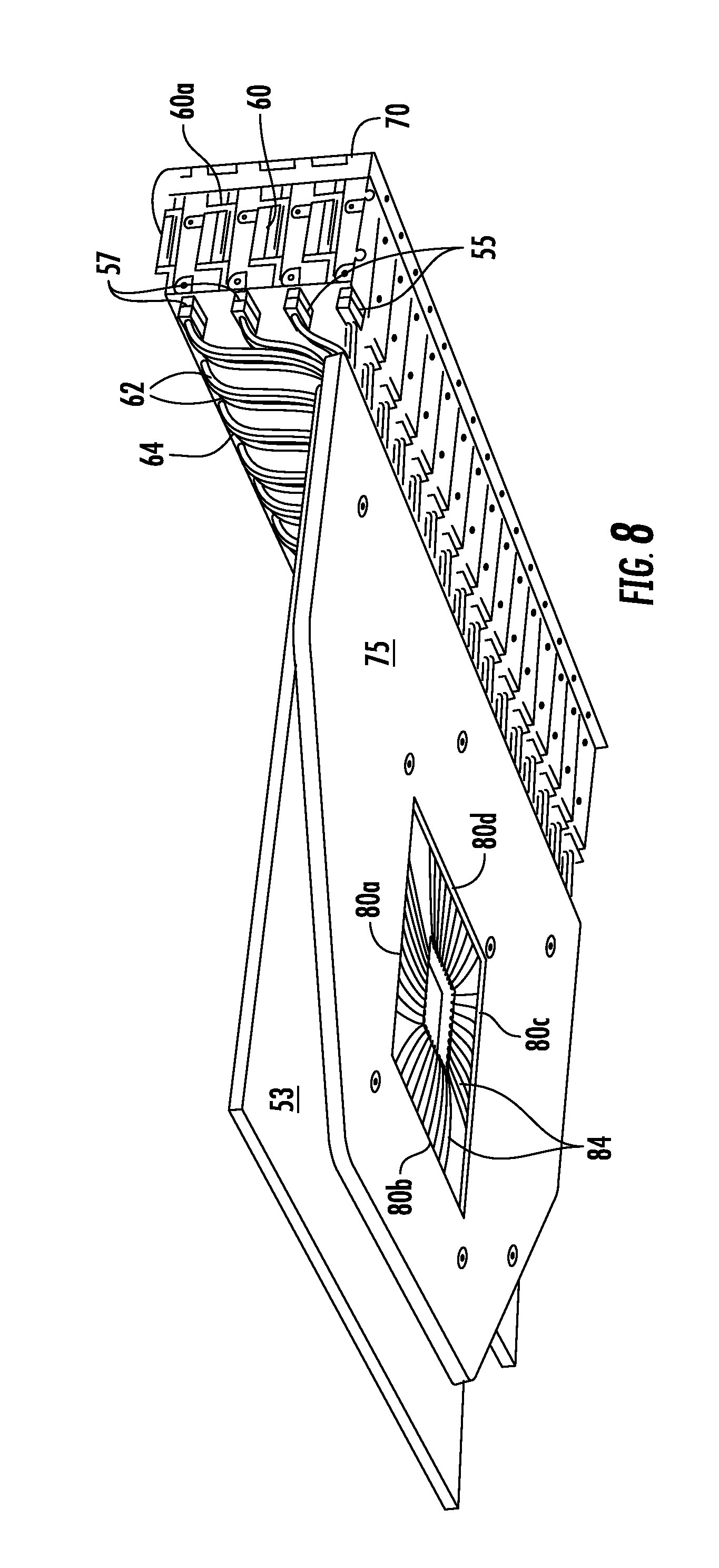
FIG. 8 is another perspective view of the embodiment depicted in FIG. 7;
FIG. 8A is a schematic sectional view of the routing assembly depicted in FIG. 8;
FIG. 8B is a perspective view of an embodiment of second connectors suitable for use in connecting to a chip package;
FIG. 9 is an elevational side view of a motherboard and chip package in position for mating with an embodiment of a routing assembly;
FIG. 9A is an elevated side view of the embodiment depicted in FIG. 9 but with the motherboard position on the tray and the side support members of the routing assembly frame shown in phantom;
FIG. 10 is a sectional schematic illustration of an embodiment of a routing assembly connected to a chip package when a tray is positioned below a motherboard; and,
FIG. 11 is a perspective view of an embodiment of system that has some connectors routing through a routing assembly and other connectors routing through a circuit board.
DETAILED DESCRIPTION
The detailed description that follows describes exemplary embodiments and is not intended to be limited to the expressly disclosed combination(s). Therefore, unless otherwise noted, features disclosed herein may be combined together to form additional combinations that were not otherwise shown for purposes of brevity.
The present disclosure is therefore directed to an integrated routing assembly at is structured to fit within the housing of an electronic device as a single element and provide multiple data transmission channels that lead directly from a chip or processor (of the ASIC or FPGA type) to an array of external connectors. The transmission channels take the form of cables fixed in place within the routing assembly, thereby eliminating the need to route the high speed channels by way of high-speed traces on a motherboard of the host device.
FIG. 1 illustrates a conventional electronic device 30, such as a router, switch, etc. that has a sheet metal housing 31 with a front wall 32 and an opposing rear wall 34. The device 30 supports within the housing, a motherboard 36 that includes various electronic components such as a chip package 38 with an associated processor 40, a power supply 42 and additional integrated circuits, connectors, capacitors, resistors, etc. The front wall 32 has a series of openings 33 that are aligned with first connectors 43 to define connector ports for the device 30. Typically, as shown in FIG. 1A, an array of first connectors 43 are mounted to the motherboard 36 at the front end thereof and enclosed within metal shielding cages 44, or adapter frames, that are placed over the connectors 43 and onto the motherboard 36. Likewise, a series of second connectors 46 are mounted along the rear edge of the motherboard 36 and aligned with openings in the rear wall of the housing 31.
In the known structure of the device of FIG. 1, the chip package 38 is connected to the first and second connectors by way of lengthy conductive traces 47 that extend from the chip package contacts through the motherboard 36 to the connectors 43, 46. Pairs of conductive traces 47 are required to define each differential signal transmission line and a third conductive trace can be used to provide an associated ground that follows the path of the signal transmission line. Each such signal transmission line is routed through or on the motherboard and such routing has certain disadvantages. FR4 is the material that is commonly used for circuit boards, and unfortunately, it becomes increasingly lossy at frequencies above 5 Ghz. Turns, bends and crossovers of these signal transmission line traces 47 are usually required to route the transmission line on the motherboard from the chip package contacts to the connectors. These directional changes in the traces can create signal reflection and noise problems, as well as additional losses. Although losses can sometimes be corrected by the use of amplifiers, repeaters and equalizers, these elements increase the cost of manufacturing of the final circuit (mother) board as well as increasing power consumption (and the cost of operation). The use of such components also complicates the layout of the circuit board because additional board space is needed to accommodate such amplifiers and repeaters and this additional board space may not be available in the intended size of the device. Custom materials for circuit boards are available that are less lossy, but the cost of these materials increase the cost of the circuit board and, consequently, the host devices in which they are used. Still further, lengthy circuit traces require increased power to drive high speed signals through them and, as such, they hamper efforts by designers to develop "green" (energy-saving) devices.
In order to overcome these actual disadvantages, we have developed an integrated routing assembly 50 that incorporates the external connector interfaces of a host device 51 into a single assembly and which provides a support for high speed differential pair signal transmission lines in the form of elongated cables 62 that extend between the connector interfaces and the chip package 88, which includes a processor 90 and may include a substrate 91, eliminating the need for high speed routing traces on the motherboard 53. Such an assembly is illustrated at 50 in FIG. 2. The assembly 50, as shown in FIGS. 2-8B, includes a front portion that accommodates a plurality of first and second connectors 55, 57 and their associated connector housings 60 in preselected arrays, which are illustrated as four horizontal rows of connector housings 60 that are stacked vertically upon each other.
The connector housings 60 define the external connector interfaces for the device 50 in the form of connector ports 54, 56 and each such connector housing 60 contains a first connector 55, 57 preferably of the receptacle style. In some instances, as illustrated, connectors ports 56 may be I/O connector ports arranged in housings 60 along a front of the host device 51 but the location and type of connector ports is not intended to be limited unless otherwise noted.
As can be appreciated, the connectors 55, 57 can be arranged in horizontal rows in an integrated fashion as in FIG. 2, where the connector housings 60 and associated heat sinks 61 are held in their horizontal extent and vertical alignment between support boards 58, by way of fasteners such as screws that extend through bosses 60a formed on the exterior of the connector housings 60. Such an arrangement can easily accommodate a face plate 70 (FIG. 3) that extends widthwise between two side supports 68 and the face plate 70 and the side supports 68 cooperatively form a frame 66. The side supports 68 have rearwardly extending channels 72a, 72b that help support a tray 75 in a cantilevered manner. The frame 66 and the tray 75 define a routing assembly 74. As depicted, the routing assembly 74 has a substantially L-shaped configuration that can be internally supported and can be inserted into a housing. It should be noted that the depicted configuration is based on the use of connector housings 60 formed via a cast construction. Alternatively, as is known, the connector housing can be formed from sheet metal that is formed in a desired construction, typically with multiple pieces being intertwined together to form the desired structure. The use of sheet metal versus cast to form a connector housing is well known and thus further discussion is not required herein.
The tray 75, as illustrated in FIG. 4 is generally planar and has a predetermined thickness and can be formed of insulative and/or conductive materials. As can be appreciated, conductive materials can provide additional shielding and thus may be desired in certain applications. The depicted tray 75 has a tray opening 76 formed therein, which is shown in the Figures as located within the perimeter of the tray 75. The tray opening 76 is shown in the Figures as having two distinct shapes and each opening has a central portion 78 that may be square or rectangular in configuration with four edges 80a-d or it may have a cruciform configuration as illustrated in FIGS. 4 & 4A in which the tray opening 76 includes four wing portions 79a-79d that communicate with the opening central portion 78 and which incorporate the four edges 80a-80d of the tray opening 76. Naturally, for versions where the tray 75 does not extend past and thus fully enclose the chip package the tray opening 76 may be replaced with a notch in the tray 75 or just the end of the tray 75.
The connectors 55, 57 that are positioned in the N by M array of connector ports 54, 56 (where both N and M can be two or more) are not shown in detail but can be any desired receptacle type having signal and ground terminals arranged in transmit and receive channel configurations to mate with opposing connectors having a plug style. For example, SFP style, QSFP style and CFP style connectors are just a few of many possible alternatives and the connectors 55, 57 are not intended to be limited to particular style of connector. It should also be noted that a single row of connectors 57 could be provide if desired. Cables 62 can be directly terminated to the terminals of each connector 55, 57 at first ends 82 of the cables 62 and are seen in FIGS. 4, 7 & 8 as being adjacent low speed wires 63 (which can be used for logic, clock, power and other circuits). The cables 62 preferably includes a pair of signal conductors in a desired spacing that are surrounded by a dielectric covering and may include an associated drain wire and/or an outer conductive covering that are enclosed in an insulative outer jacket so as to form a transmission line. The cables 62 help maintain the ordered geometry of the signal conductors throughout their lengths as they traverse from the chip package 88 to the connectors 55, 57. Because this geometry remains ordered through their length, the cables 62 may easily be turned or bent or crossed in their paths without introducing problematic signal reflection or impedance discontinuities into the transmission lines.
Both the cables 62 and low speed wires 63 are terminated directly at their first ends 82 to the connectors 55, 57. This make it possible to eliminate a direct connection with the motherboard 53 and allows for structures that can be readily stacked while still providing acceptable air flow and while avoiding impedance discontinuities which normally occur at a connector-circuit board mounting interface. The cables 62 are illustrated as arranged in rows at the rear of the connector housings 60. The cables 62 are arranged in rows as best shown in FIGS. 8A, 9 & 9A, with the cables 62 and low speed wires 63 of the lower connector housing rows arranged inwardly of the topmost connector housing row. This promotes orderly arrangement of the cables 62 from the connectors 55, 57 to the tray 75. In the assembly 50 depicted (in FIGS. 9 and 9A) the cables 62 associated with the top three rows of connectors 54, 56 and connector ports 55, 57 are seen to have a general S-shaped configuration extending downward to the level of the tray 75 and into the substrate at the front end thereof, while the cables in the bottommost row extend almost horizontally into the tray 75.
The cables 62 are illustrated in FIG. 5 as having first ends 82 extending from the connectors 55, 57 toward the tray 75. The second ends 84 of the cables 62 extend into the tray opening 76 as illustrated where they are terminated to connectors 86 that will mate with the chip package 88. The connectors 86 can be configured to connect to a connector mounted on or adjacent a substrate 91 (such as connector 95 discussed below) or can be configured to press directly onto the substrate 91 (or a supporting motherboard adjacent the substrate). The second ends 84 of the cables 62 exit the tray 75 to enter the tray opening 76. In an embodiment, the chip package 88 is disposed on the motherboard 53, and the chip package 88 includes a plurality of contacts in the form of receptacle style connectors 95 which are preferably arranged around the perimeter thereof and aligned with the tray opening 76 so as to allow for mating with connectors 86 at the cable second ends 84. In another aspect, the chip package 88 may be included as part of the overall routing assembly 74. (FIGS. 2 and 2A.)
It should be noted that the tray 75 can be positioned above the circuit board, such as is depicted in FIGS. 4A-6. Alternatively, as shown in FIGS. 7-10, the tray 75 can be positioned below the motherboard 53. In such a configuration, as illustrated in FIGS. 3 & 3A, the area above the motherboard 53 is free to accommodate thermal transfer members 93, which can include heat spreaders and/or heat sinks having perimeters larger than that of the processor 90 because the integration of the cables 62 into the tray 75 frees up most, if not all, of the space above the tray 75 for other uses.
The cables 62 (and low speed wires 64) may be positioned as part of the tray 75 in a variety of ways that suitably holds them in place from where they enter the routing assembly 74, such as along a leading edge 83 of the tray 75 to where they exit the tray 75 and enter the tray opening 76. The cables 62 can be accommodated in the tray 75 by enclosing the cables 62 in the tray 75. The body portions of the cables 62 are preferably completely surrounded by the tray 75 so that the two form an integral part that can be provided in the routing assembly 74. One routing pattern of the cables 62 is illustrated in FIG. 5, which has the upper portion of the tray 75 removed for clarity to show the paths in which the cables 62 are laid.
The cables 62 can be terminated at their second ends 84 to the aforementioned connectors 86 before the forming of the tray 75. Inasmuch as the first ends of the cables 62 are directly terminated to the terminals of the cable direct connectors 55, the second connectors 86 permit the cables 62 to be directly connected to the chip package 88, thereby completely bypassing the motherboard 53 as a routing support. In instances where the tray 75 is located above the motherboard 53, the connectors 86 are positioned around the chip package 88 and are preferably arranged along the edges of the tray opening 76. Or, as illustrated in FIGS. 7-10, the connectors 86 may be configured to mate with the chip package 88 from below, it being understood that such a configuration may be preferred in certain circumstances.
In such an instance, the routing assembly 74 may be inserted into the host device housing and the motherboard 53 is placed in the housing of the device 51 over the tray 75, where it may be spaced apart from and below the motherboard by standoffs 92 or the like. FIG. 6 illustrates the connectors 86 and their associated housings 87 facing toward the substrate 91 in the tray opening 76 so as to make contact with the substrate 91 so as to provide a connection to processor 90 (or alternatively with a motherboard 53 that supports the substrate 91, as shown in FIG. 10). Naturally, a similar configuration can be provided below for a tray 75 positioned below the motherboard 53. The connector housings 87 may take the form of chiclets which can house as few as a single pair of signal conductors. As can be appreciated, the connector housing 87 can easily mate with receptacle connectors 95 on the motherboard 53 or substrate 91. In addition, if the cables 62 are fixed in position in the tray so that the cables 62 only extend a short distance out of the tray 75 before terminating to connectors 86 then the structure also helps ensure the connectors 86 are properly aligned with the motherboard or chip package 88 (and any corresponding mating receptacle connectors) and the alignment can make assembly much easier. The connectors 86 and the mating receptacle connectors may be provided with a low profile so as to fit within the tray opening 76 and potentially will not project outside of the tray opening 76, thus minimizing the space requirements of the routing assembly 74. As can be appreciated, the cables extend into the opening from at least two directions and preferably will extend from multiple edges of the tray.
Such a structure is shown schematically in the sectional diagrams of FIGS. 8A & 10, where the board connectors 95 are shown in contact with conductive vias 96 the extend through the motherboard 53 to connect with the substrate 91. As can be appreciated, a BGA structure can attach the substrate 91 to the motherboard 53. It can be seen that the second ends 84 of the cables 62 and their corresponding connectors 86 can be accommodated within the volume of the tray opening 76 so as not to unduly increase the height of the device 51. As can be appreciated, the depicted connectors 86 have a mating direction that is transverse to the tray.
FIG. 11 illustrates another embodiment of a routing assembly 100 of the present disclosure in which connector ports 102 are in place on the motherboard 104 and connectors 107 are desired along a front 110. The connector ports 102 are arranged in two horizontal rows within their shielding cages 103 and in place upon the motherboard 104 that has a chip package 106 in place. The routing assembly 100 has two rows of connector ports 107 held in the frame at a height that permits the assembly to be placed over the existing connector ports 102 and utilize the high speed advantages of the cables 62 of the routing assembly 100 for that set of connector ports. This structure will permit a combination of connector ports connected to a circuit board and connector ports connected to a chip package via cables, thus providing flexibility in system architecture. While the depicted embodiment illustrate a system that includes two rows of connector ports mounted on the circuit board and two rows of connector ports provided by the routing assembly, alternative embodiments could have 1 row of each type or could vary the number of rows, depending on system needs.
The disclosure provided herein describes features in terms of preferred and exemplary embodiments thereof. Numerous other embodiments, modifications and variations within the scope and spirit of the appended claims will occur to persons of ordinary skill in the art from a review of this disclosure.
* * * * *
References
D00000
D00001
D00002
D00003
D00004
D00005
D00006
D00007
D00008
D00009
D00010
D00011
D00012

D00013

D00014

D00015

XML
uspto.report is an independent third-party trademark research tool that is not affiliated, endorsed, or sponsored by the United States Patent and Trademark Office (USPTO) or any other governmental organization. The information provided by uspto.report is based on publicly available data at the time of writing and is intended for informational purposes only.
While we strive to provide accurate and up-to-date information, we do not guarantee the accuracy, completeness, reliability, or suitability of the information displayed on this site. The use of this site is at your own risk. Any reliance you place on such information is therefore strictly at your own risk.
All official trademark data, including owner information, should be verified by visiting the official USPTO website at www.uspto.gov. This site is not intended to replace professional legal advice and should not be used as a substitute for consulting with a legal professional who is knowledgeable about trademark law.