Method and device for ion mobility separation
Ibrahim , et al. Sept
U.S. patent number 10,424,474 [Application Number 15/759,194] was granted by the patent office on 2019-09-24 for method and device for ion mobility separation. This patent grant is currently assigned to Battelle Memorial Institute. The grantee listed for this patent is Battelle Memorial Institute. Invention is credited to Sandilya V. B. Garimella, Yehia M. Ibrahim, Richard D. Smith.


| United States Patent | 10,424,474 |
| Ibrahim , et al. | September 24, 2019 |
Method and device for ion mobility separation
Abstract
Methods and devices for ion separations or manipulations in gas phase are disclosed. The device includes a non-planar surface having a first, second and third region. An inner arrays of electrodes is positioned on the first region. A first set of electrodes of the inner array of electrodes is configured to receive RF voltages and generate a first potential upon the receipt of the RF voltage. A first and second outer arrays of electrodes are coupled to the second and third region, respectively. The first and second outer arrays are configured to receive a first DC voltage and generate a second potential upon the receipt of the first DC voltages. The first and second generated potential manipulate movement of ions.
| Inventors: | Ibrahim; Yehia M. (Richland, WA), Garimella; Sandilya V. B. (Richland, WA), Smith; Richard D. (Richland, WA) | ||||||||||
|---|---|---|---|---|---|---|---|---|---|---|---|
| Applicant: |
|
||||||||||
| Assignee: | Battelle Memorial Institute
(Richland, WA) |
||||||||||
| Family ID: | 56080454 | ||||||||||
| Appl. No.: | 15/759,194 | ||||||||||
| Filed: | May 2, 2016 | ||||||||||
| PCT Filed: | May 02, 2016 | ||||||||||
| PCT No.: | PCT/US2016/030455 | ||||||||||
| 371(c)(1),(2),(4) Date: | March 09, 2018 | ||||||||||
| PCT Pub. No.: | WO2017/044159 | ||||||||||
| PCT Pub. Date: | March 16, 2017 |
Prior Publication Data
| Document Identifier | Publication Date | |
|---|---|---|
| US 20180254178 A1 | Sep 6, 2018 | |
Related U.S. Patent Documents
| Application Number | Filing Date | Patent Number | Issue Date | ||
|---|---|---|---|---|---|
| 14851935 | Jul 11, 2017 | 9704701 | |||
| Current U.S. Class: | 1/1 |
| Current CPC Class: | H01J 49/26 (20130101); H01J 49/0013 (20130101); H01J 49/40 (20130101); H01J 49/022 (20130101); G01N 27/622 (20130101) |
| Current International Class: | H01J 49/26 (20060101); H01J 49/02 (20060101); H01J 49/00 (20060101); H01J 49/40 (20060101); G01N 27/62 (20060101) |
| Field of Search: | ;250/281,282,283,290 |
References Cited [Referenced By]
U.S. Patent Documents
| 4777363 | October 1988 | Eiceman et al. |
| 5206506 | April 1993 | Kirchner |
| 5572035 | November 1996 | Franzen |
| 5834771 | November 1998 | Yoon et al. |
| 6107628 | August 2000 | Smith et al. |
| 6417511 | July 2002 | Russ, IV |
| 6891157 | May 2005 | Bateman et al. |
| 6960760 | November 2005 | Bateman et al. |
| 7095013 | August 2006 | Bateman et al. |
| 7151255 | December 2006 | Weiss et al. |
| 7157698 | January 2007 | Makarov et al. |
| 7180078 | February 2007 | Pau et al. |
| 7365317 | April 2008 | Whitehouse et al. |
| 7391021 | June 2008 | Stoermer et al. |
| 7405401 | July 2008 | Hoyes |
| 7548818 | June 2009 | Kieser |
| 7786435 | August 2010 | Whitehouse et al. |
| 7838826 | November 2010 | Park |
| 7872228 | January 2011 | Kim et al. |
| 7888635 | February 2011 | Belov et al. |
| 7928375 | April 2011 | Mangan et al. |
| 8003934 | August 2011 | Hieke |
| 8049169 | November 2011 | Satake et al. |
| 8222597 | July 2012 | Kim et al. |
| 8319180 | November 2012 | Nikolaev et al. |
| 8373120 | February 2013 | Verentchikov |
| 8389933 | March 2013 | Hoyes |
| 8410429 | April 2013 | Franzen et al. |
| 8581181 | November 2013 | Giles |
| 8809769 | August 2014 | Park |
| 8835839 | September 2014 | Anderson |
| 8901490 | December 2014 | Chen et al. |
| 8907273 | December 2014 | Chen et al. |
| 8969800 | March 2015 | Tolmachev et al. |
| 9704701 | July 2017 | Ibrahim |
| 9812311 | November 2017 | Anderson et al. |
| 9966244 | May 2018 | Anderson et al. |
| 2001/0035498 | November 2001 | Li |
| 2003/0132379 | July 2003 | Li |
| 2004/0026611 | February 2004 | Bateman et al. |
| 2004/0089803 | May 2004 | Foley |
| 2004/0222369 | November 2004 | Makarov et al. |
| 2005/0040327 | February 2005 | Lee et al. |
| 2005/0109930 | May 2005 | Hill, Jr. et al. |
| 2007/0138384 | June 2007 | Keiser |
| 2008/0073515 | March 2008 | Schoen |
| 2009/0173880 | July 2009 | Bateman et al. |
| 2009/0206250 | August 2009 | Wollnik |
| 2011/0049357 | March 2011 | Giles |
| 2011/0192969 | August 2011 | Verentchikov |
| 2014/0061457 | March 2014 | Berdnikov et al. |
| 2014/0124663 | May 2014 | Green et al. |
| 2014/0145076 | May 2014 | Park |
| 2014/0299766 | October 2014 | Anderson et al. |
| 2015/0028200 | January 2015 | Green et al. |
| 2015/0364309 | December 2015 | Welkie |
| 2016/0027604 | January 2016 | Cho et al. |
| 2016/0049287 | February 2016 | Ding et al. |
| 2016/0071715 | March 2016 | Anderson et al. |
| 2017/0076931 | March 2017 | Ibrahim et al. |
| 2017/0125229 | May 2017 | Giles et al. |
| 2018/0061621 | March 2018 | Anderson et al. |
| 2014251354 | Nov 2017 | AU | |||
| 2016320584 | Apr 2018 | AU | |||
| 2016335524 | May 2018 | AU | |||
| 2908936 | Oct 2014 | CA | |||
| 2997910 | Mar 2017 | CA | |||
| 3000341 | Apr 2017 | CA | |||
| 1361922 | Jul 2002 | CN | |||
| 101126738 | Feb 2008 | CN | |||
| 102163531 | Aug 2011 | CN | |||
| 102945786 | Feb 2013 | CN | |||
| 201680069722.X | Aug 2016 | CN | |||
| 105264637 | Sep 2017 | CN | |||
| 107507751 | Dec 2017 | CN | |||
| 108352288 | Jul 2018 | CN | |||
| 112013004733 | Jun 2015 | DE | |||
| 1566828 | Aug 2005 | EP | |||
| 1825495 | Aug 2007 | EP | |||
| 2065917 | Jun 2009 | EP | |||
| 2913839 | Sep 2015 | EP | |||
| 2984675 | Feb 2016 | EP | |||
| 3347913 | Jul 2018 | EP | |||
| 3359960 | Aug 2018 | EP | |||
| 2440970 | Feb 2008 | GB | |||
| 2506362 | Apr 2014 | GB | |||
| 2002-015699 | Jan 2002 | JP | |||
| 2009532822 | Sep 2009 | JP | |||
| 2009535759 | Oct 2009 | JP | |||
| 2009537070 | Oct 2009 | JP | |||
| 2011529623 | Dec 2011 | JP | |||
| 2012503286 | Feb 2012 | JP | |||
| 2016514896 | May 2016 | JP | |||
| 2018-518405 | Aug 2016 | JP | |||
| 2018528427 | Sep 2018 | JP | |||
| 11201801852Q | May 2016 | SG | |||
| 11201802494Q | Aug 2016 | SG | |||
| 11201508277X | Feb 2018 | SG | |||
| WO 2006/064274 | Jun 2006 | WO | |||
| WO 2007/133469 | Nov 2007 | WO | |||
| WO 2010/014077 | Feb 2010 | WO | |||
| WO 2010/032015 | Mar 2010 | WO | |||
| WO 2011/089419 | Jul 2011 | WO | |||
| WO 2012/116765 | Sep 2012 | WO | |||
| WO 2013/018529 | Feb 2013 | WO | |||
| WO 2014/048837 | Apr 2014 | WO | |||
| WO 2014/168660 | Oct 2014 | WO | |||
| WO 2015/056872 | Apr 2015 | WO | |||
| WO 2015/097462 | Jul 2015 | WO | |||
| WO 2016/069104 | May 2016 | WO | |||
| WO 2017/044159 | Mar 2017 | WO | |||
| WO 2017/062102 | Apr 2017 | WO | |||
Other References
|
English translation of the first Chinese office action from corresponding Chinese patent application No. 201480032436.7, dated Oct. 14, 2016, 5 pages. cited by applicant . English translation of the search report from corresponding Chinese patent application No. 201480032436.7, dated Sep. 29, 2016, 2 pages. cited by applicant . European Search Report for European Patent Application No. 14782685.3, dated Oct. 25, 2016. cited by applicant . Examination Report No. 1 for related Australian Application No. 2016320584, dated Jun. 27, 2018, 3 pages. cited by applicant . First Office Action for related Canadian Application No. 2,997,910, dated May 4, 2018, 4 pages. cited by applicant . Hamid, et al., "Characterization of Travelling Wave Ion Mobility Separations in Structures for Lossless Ion Manipulations," Analytical Chemistry, 87(22):11301-11308 (Nov. 2015). cited by applicant . International Search Report and Written Opinion for PCT/US2016/047070 (dated Nov. 7, 2016). cited by applicant . International Search Report and Written Opinion for related International Application No. PCT/US2014/011291, dated Jun. 6, 2014, 2 pages. cited by applicant . Search Report from corresponding Singapore patent application No. 11201508277X, dated Mar. 6, 2016, 7 pages. cited by applicant . Tolmachev, et al., "Characterization of Ion Dynamics in Structures for Lossless Ion Manipulations," Analytical Chemistry, 86(18):9162-9168 (Sep. 2014). cited by applicant . International Search Report and Written Opinion issued in related International Application No. PCT/US2016/030455, dated Jul. 25, 2016, 19pp. cited by applicant . First Office Action for related Japanese Application No. 2018-513012, dated Aug. 2, 2018, 2 pages; with English translation, 2 pages. cited by applicant . First Office Action for related Chinese Application No. 201680065673.2, dated Sep. 30, 2018, 6 pages. cited by applicant . Chen, et al., "Mobility-Selected Ion Trapping and Enrichment Using Structures for Lossless Ion Manipulations", Analytical Chemistry, Jan. 2016, 88, pp. 1728-1733. cited by applicant . Deng et al., "Serpentine Ultralong Path with Extended Routing (SUPER) High Resolution Traveling Wave Ion Mobility-MS using Structures for Lossles Ion Manipulations", Analytical Chemistry, Mar. 2017, 89, pp. 4628-4634. cited by applicant . Examination Report No. 2 for related Australian Application No. 2016320584, dated Sep. 3, 2018, 2 pages. cited by applicant . Examination Report No. 1 for related Australian Application No. 2016335524, dated May 15, 2018, 4 pages. cited by applicant . First Office Action for related Canadian Application No. 3,000,341, dated Jul. 30, 2018, 5 pages. cited by applicant . First Office Action for Chinese Application No. 201680065673.2, dated Sep. 30, 2018, 6 pages (English translation not yet available). cited by applicant . International Search Report and Written Opinion for related International Application No. PCT/US2018/041607, dated Sep. 20, 2018, 18 pp. cited by applicant . Webb et al., "Mobility-Resolved Ion Selection in Uniform Drift Field Ion Mobility Spectrometry/Mass Spectrometry: Dynamic Switching in Structures for Lossless Ion Manipulations," Analytical Chemistry, Oct. 2014, 86, 9632-9637. cited by applicant . Wojcik et al., "Lipid and Glycolipid Isomer Analyses Using Ultra-High Resolution Ion Mobility Spectrometry Separations", International Jouranl of Molecular Sciences, Jan. 2017, 18, 12 pp. cited by applicant . Written Opinion from the Intellectual Property Office of Singapore for related Application No. 11201802494Q, dated Aug. 21, 2018, 8 pages. cited by applicant . Written Opinion from the Intellectual Property Office of Singapore for related Application No. 11201801852Q, dated Nov. 22, 2018, 26 pages. cited by applicant . International Search Report and Written Opinion for related International Application No. PCT/US2018/046752, dated Dec. 4, 2018, 12 pp. cited by applicant . English translation of the first Chinese office action from corresponding Chinese patent application No. 201710799275.X, dated Nov. 2, 2018, 12 pages. cited by applicant. |
Primary Examiner: Ippolito; Nicole M
Attorney, Agent or Firm: Klarquist Sparkman, LLP
Government Interests
STATEMENT REGARDING FEDERALLY SPONSORED RESEARCH OR DEVELOPMENT
This invention was made with Government support under Contract DE-AC0576RL01830 awarded by the U.S. Department of Energy. The Government has certain rights in the invention.
Claims
We claim:
1. An ion mobility manipulation device comprising: a non-planar surface comprising a first, second and third region; an inner array of electrodes positioned on the first region, a first set of electrodes of the inner array of electrodes configured to receive RF voltages and generate a first potential upon the receipt of the RF voltage; and a first and second outer arrays of electrodes coupled to the second and third region, respectively, the first and second outer arrays configured to receive a first DC voltage and generate a second potential upon the receipt of the first DC voltages, wherein the first and second generated potential manipulate movement of ions.
2. The device of claim 1, wherein the non-planer surface is curved to form an ion channel, wherein movement of ions occurs in the ion channel.
3. The device of claim 2, wherein the inner array of electrodes, the first and second outer arrays of electrodes and the ionization separation channel extend along a length of the device.
4. The device of claim 2, wherein the first outer array of electrodes is positioned on a first side of the inner array of electrodes, and the second outer array of electrodes is positioned on a second side of the inner array of electrodes.
5. The device of claim 2, wherein the inner array of electrodes comprises a second set of electrodes configured to receive a second DC voltage.
6. The device of claim 5, wherein the second set of electrodes generate a gradient potential that drives the ions in the ion channel.
7. The device of claim 5, wherein electrodes of the first set of electrodes are separated by electrodes of the second set of electrodes.
8. The device of claim 2, wherein the first set of electrodes of the inner array of electrodes is configured to receive a second DC voltage.
9. The device of claim 8, wherein RF voltages received by neighboring electrodes of the first set of electrodes are phase shifted.
10. The device of claim 1, wherein the second potential confines the ions along a lateral direction associated with the device.
11. The device of claim 1, wherein RF voltages received by adjacent electrodes of the first set of electrodes have a phase difference.
12. The device of claim 11, wherein the phase difference is 180 degrees.
13. The device of claim 1, wherein the first generated potential inhibits the ions from approaching the non-planer surface.
14. The device of claim 1, further comprising a cover enclosure, wherein the cover enclosure is configured to guard against an external potential.
15. The device of claim 14, wherein the cover enclosure is configured to receive a potential.
16. The device of claim 1 wherein the non-planar surface is one of the following shapes: cylindrical, a spiral, a funnel, hemispherical, or elliptical.
Description
CROSS-REFERENCE TO RELATED APPLICATIONS
This application is a U.S. National Stage of International Application No. PCT/US2016/030455, filed May 2, 2016, which was published in English under PCT Article 21(3), which in turn claims priority to U.S. application Ser. No. 14/851,935, filed Sep. 11, 2015 now U.S. Pat. No. 9,704,701, titled "METHOD AND DEVICE FOR ION MOBILITY SEPARATIONS" hereby incorporated by reference in its entirety for all of its teachings.
TECHNICAL FIELD
This invention relates to ion mobility separations and other ion manipulations in the gas phase. More specifically, this invention relates to an ion mobility separation method and ion manipulations in a device having a single, non-planar surface containing electrodes.
BACKGROUND
The utility of mass spectrometry expands with the capability to conduct more complex ion manipulations. Current ion mobility technologies and ion manipulations rely on surrounding surfaces that serve to define the electric fields. However, these approaches can become ineffective when, for example, trying to miniaturize these devices for field deployment. In addition, it is extremely difficult to achieve high ion mobility spectrometry (IMS) resolution by extending the drift length traveled by ions in a reasonable and practical physical length. Hence, the utility of IMS is hindered by conventional ion optics designs.
What is needed is an ion mobility separation or manipulation device with an open structure, including an ion separation channel, and which also prevents ion losses.
SUMMARY
The present invention is directed to an ion mobility separation or manipulation device that includes a single surface. The single surface is non-planar or not flat. The device also includes arrays of electrodes coupled to the surface. The device further includes a combination of RF and DC voltages applied to arrays of electrodes to create confining and driving fields that move ions through the device. The surface can have, in one embodiment, arrays of electrodes on each side of the surface.
In one embodiment, one or more electrodes or others surfaces external to the device can help partially or fully define or affect the electric fields created by the electrodes on the surface. These external electrodes or surfaces, which have voltages applied to them, allow different or more complex fields to be established or created. This would allow, for example, one array of electrodes on the surface to be turned off while the other array is turned on. This can be useful for, among other things, peak compression or the bunching of ions. In one embodiment, the arrays of electrodes coupled to the surface extend above the surface, and may also vary in the distance above the surface. Further, the one or more arrays of electrodes coupled to the surface can be turned on or turned off by the external surfaces and/or electrodes.
The single, non-planar surface can be of many different shapes. The surface can have a curved, cylindrical, spiral, funnel, hemispherical, elliptical, or non-symmetrical shape.
In one embodiment, a transparent enclosure or cover is disposed on the device. A voltage can be applied to the cover to guard against interfering potential from, e.g., ground or nearby electronics. In one embodiment, the device is located in a partially or completely transparent enclosure or cover.
In one embodiment, the arrays of electrodes include one or more arrays of inner RF electrodes and a plurality of arrays of outer DC electrodes. The inner array of RF electrodes and the outer arrays of DC electrodes extend substantially along the length of the surface. In one embodiment, a first outer array of DC electrodes is positioned on one side of the inner array of RF electrodes, and a second outer array of DC electrodes is positioned on the other side of the inner array of electrodes.
In one embodiment, the DC voltages are applied to the first and second outer electrodes arrays, and the RF voltages are applied to the inner array of electrodes.
In one embodiment, the RF waveform on at least one inner electrode array is out of phase with RF waveform on a neighboring inner RF electrode array. The RF voltage applied to each inner RF electrode array may be phase shifted with its neighboring inner electrode array to form a pseudopotential. In one embodiment, the RF voltage applied to the inner electrode array is approximately 180 degrees out of phase with its neighboring inner electrode array to form the pseudopotential.
The device may further comprise one or more arrays of inner DC electrodes that extend substantially along the length of the surface, in either a linear or non-linear path. Each inner array of DC electrodes is positioned between an adjacent pair of the RF electrode arrays. A RF waveform on at least one inner array of RF electrodes is out of phase with RF waveform on a neighboring or adjacent inner array of RF electrodes.
In one embodiment, a first DC voltage applied to the outer array of DC electrodes is the same, and a second DC voltage applied to the inner array of DC electrodes is a DC gradient or different across the inner DC arrays.
In one embodiment, a first DC voltage applied to the outer array of DC electrodes is different across the outer array or is a DC gradient, and a second DC voltage applied to the inner array of DC electrodes is a DC gradient or different across the inner DC arrays.
The first DC voltage may have a higher or lower amplitude than the second DC field.
In one embodiment, the inner array of DC electrodes is misaligned or offset from the outer array of electrodes.
In one embodiment, a DC voltage is superimposed on at least one of the inner arrays of RF electrodes.
The device may be coupled to at least one of the following: a charge detector, ion image detector, an optical detector, and a mass spectrometer.
In one embodiment, the ions are introduced from outside the device at an angle to the device.
The ions may be formed inside or outside of the device using at least one of the following: photoionization, Corona discharge, laser ionization, electron impact, field ionization, chemical ionization, and electrospray.
The DC voltages may be static DC voltages or time-dependent DC potentials or waveforms.
In one embodiment, the surface is formed by curving a flexible printed circuit board material, three-dimensional printing, or other means to deposit conductive material on a non-conductive surface.
In another embodiment of the present invention, a method of moving and separating ions in gas phase is disclosed. The method includes coupling arrays of electrodes to a single, non-planar surface. The method also includes applying a combination of RF and DC voltages to the arrays of electrodes to create confining and driving fields that move ions through the single curved or non-planar surface.
In another embodiment of the present invention, an ion mobility separation device is disclosed. The device includes a single, non-planar surface. The device also includes arrays of electrodes which include one or more arrays of inner RF electrodes and a plurality of arrays of outer DC electrodes. The inner array of RF electrodes and the outer array of DC electrodes extend substantially along the length of the surface. A first and second outer array of DC electrodes is positioned on either side of the inner array of RF electrodes. The device further includes one or more arrays of inner DC electrodes that extend substantially along the length of the surface. Each inner array of DC electrodes is positioned between an adjacent pair of inner RF electrode arrays. A combination of RF and DC voltages are applied to the arrays of electrodes to create confining and driving fields that move ions through the device.
In one embodiment, a RF waveform on at least one inner array of RF electrodes is out of phase with RF waveform on a neighboring or adjacent inner array of RF electrodes.
A first DC voltage applied to the outer array of DC electrodes is the same or different, and a second DC voltage applied to the inner array of DC electrodes is a DC gradient or different across the inner DC arrays.
In another embodiment of the present invention, an ion mobility device is disclosed. The device includes a single, non-planar surface. The device also includes arrays of inner RF electrodes and a plurality of arrays of outer DC electrodes, coupled to the single surface, wherein the inner array of RF electrodes and the outer array of DC electrodes extend substantially along the length of the single surface. A first and second outer array of DC electrodes is positioned on either side of the inner array of RF electrodes. A combination of RF and DC voltages applied to the arrays of electrodes to create confining and driving fields that move ions through the device, and a DC field is superimposed on the inner arrays of RF electrodes to further confine and move the ions through the device.
In another embodiment, the device can include two or more non-planar surfaces with different orientations to each other that provide a "waterfall" effect of the ions moving through each surface.
BRIEF DESCRIPTION OF THE DRAWINGS
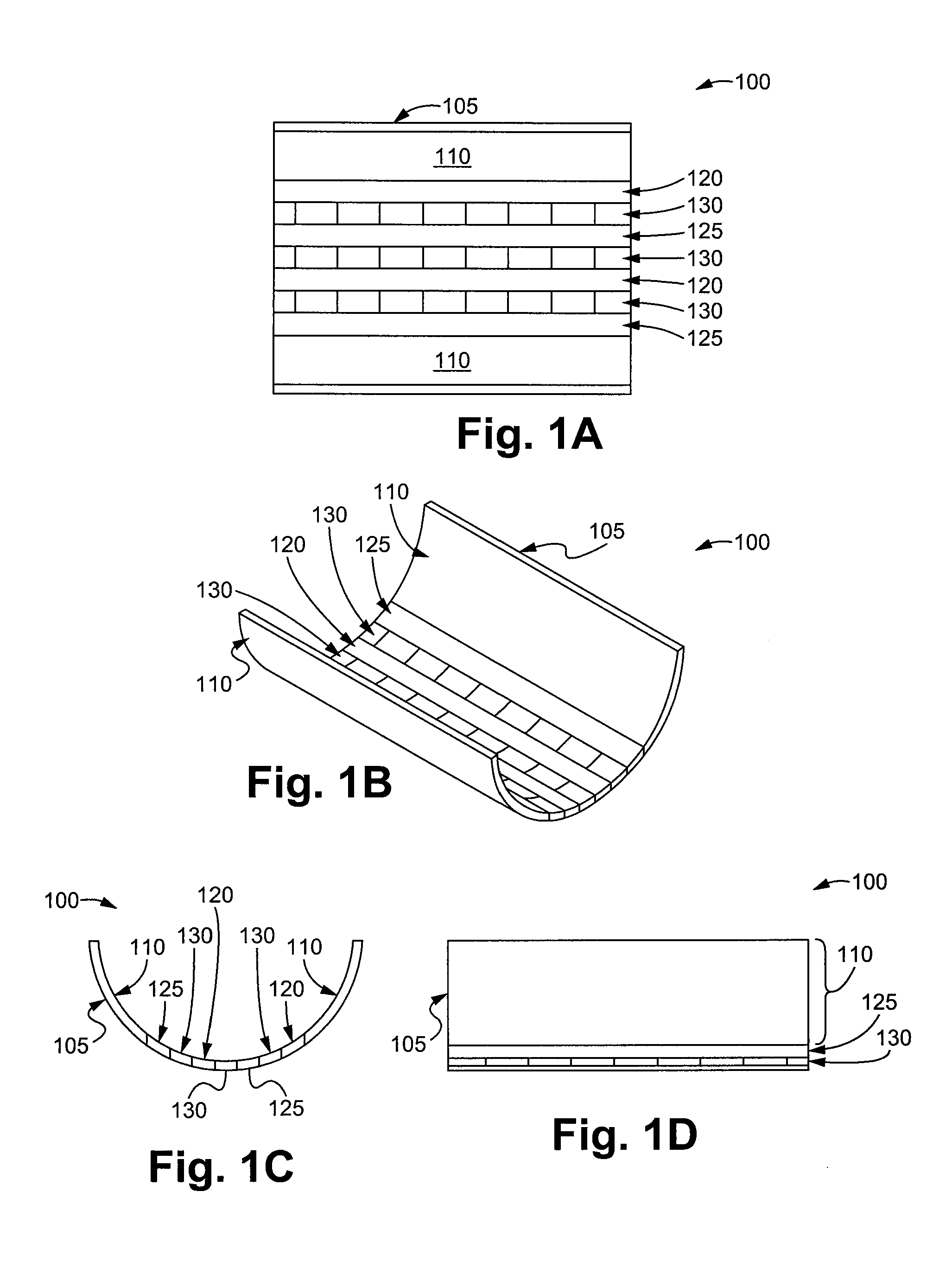
FIG. 1A is a top view schematic diagram of an ion mobility device having a single curved or non-planar surface containing arrays of outer and inner DC electrodes and arrays of RF electrodes of opposite phase on either side of the inner DC electrodes, in accordance with one embodiment of the present invention.
FIG. 1B is a perspective view schematic diagram of an ion mobility device having a single curved or non-planar surface containing arrays of outer and inner DC electrodes and arrays of RF electrodes of opposite phase on either side of the inner DC electrodes, in accordance with one embodiment of the present invention.
FIG. 1C is a front view schematic diagram of an ion mobility device having a single curved or non-planar surface containing arrays of outer and inner DC electrodes and arrays of RF electrodes of opposite phase on either side of the inner DC electrodes, in accordance with one embodiment of the present invention.
FIG. 1D is a side view schematic diagram of an ion mobility device having a single curved or non-planar surface containing arrays of outer and inner DC electrodes and arrays of RF electrodes of opposite phase on either side of the inner DC electrodes, in accordance with one embodiment of the present invention.
FIG. 2A is a top view schematic diagram of an ion mobility device having a single curved or non-planar surface containing arrays of outer DC electrodes and inner RF electrodes with a superimposed DC field on the inner array of RF electrodes, in accordance with one embodiment of the present invention.
FIG. 2B is a perspective view schematic diagram of an ion mobility device having a single curved or non-planar surface containing arrays of outer DC electrodes and inner RF electrodes with a superimposed DC field on the inner array of RF electrodes, in accordance with one embodiment of the present invention.
FIG. 2C is a front view schematic diagram of an ion mobility device having a single curved or non-planar surface containing arrays of outer DC electrodes and inner RF electrodes with a superimposed DC field on the inner array of RF electrodes, in accordance with one embodiment of the present invention.
FIG. 2D is a side view schematic diagram of an ion mobility device having a single curved or non-planar surface containing arrays of outer DC electrodes and inner RF electrodes with a superimposed DC field on the inner array of RF electrodes, in accordance with one embodiment of the present invention.
FIG. 3A is a top view schematic diagram of an ion mobility device having a single curved or non-planar surface containing arrays of outer and inner DC electrodes with different DC fields or a DC gradient applied across the electrodes and arrays of RF electrodes of opposite phase on either side of the inner DC electrodes, in accordance with one embodiment of the present invention.
FIG. 3B is a perspective view schematic diagram of an ion mobility device having a single curved or non-planar surface containing arrays of outer and inner DC electrodes with different DC fields or a DC gradient applied across the electrodes and arrays of RF electrodes of opposite phase on either side of the inner DC electrodes, in accordance with one embodiment of the present invention.
FIG. 3C is a front view schematic diagram of an ion mobility device having a single curved or non-planar surface containing arrays of outer and inner DC electrodes with different DC fields or a DC gradient applied across the electrodes and arrays of RF electrodes of opposite phase on either side of the inner DC electrodes, in accordance with one embodiment of the present invention.
FIG. 3D is a side view schematic diagram of an ion mobility device having a single curved or non-planar surface containing arrays of outer and inner DC electrodes with different DC fields or a DC gradient applied across the electrodes and arrays of RF electrodes of opposite phase on either side of the inner DC electrodes, in accordance with one embodiment of the present invention.
FIG. 4A is a top view schematic diagram of an ion mobility device having a single curved or non-planar surface containing arrays of misaligned or offset outer and inner DC electrodes with different DC fields or a DC gradient applied across the electrodes and arrays of RF electrodes of opposite phase on either side of the inner DC electrodes, in accordance with one embodiment of the present invention.
FIG. 4B is a perspective view schematic diagram of an ion mobility device having a single curved or non-planar surface containing arrays of misaligned or offset outer and inner DC electrodes with different DC fields or a DC gradient applied across the electrodes and arrays of RF electrodes of opposite phase on either side of the inner DC electrodes, in accordance with one embodiment of the present invention.
FIG. 4C is a front view schematic diagram of an ion mobility device having a single curved or non-planar surface containing arrays of misaligned or offset outer and inner DC electrodes with different DC fields or a DC gradient applied across the electrodes and arrays of RF electrodes of opposite phase on either side of the inner DC electrodes, in accordance with one embodiment of the present invention.
FIG. 4D is a side view schematic diagram of an ion mobility device having a single curved or non-planar surface containing arrays of misaligned or offset outer and inner DC electrodes with different DC fields or a DC gradient applied across the electrodes and arrays of RF electrodes of opposite phase on either side of the inner DC electrodes, in accordance with one embodiment of the present invention.
FIG. 5 shows a cross section of the ion mobility device of FIG. 1, with ions moving through the device at a distance from the surface, in accordance with one embodiment of the present invention.
FIG. 6 is a plot of ion counts over arrival time using the embodiment of FIG. 1, showing separation of two ions with different mass-to-charge ratios according to their mobilities.
FIG. 7A is a three-dimensional schematic diagram of the device of FIG. 1, with ions moving through the device at a distance from the surface, in accordance with one embodiment of the present invention.
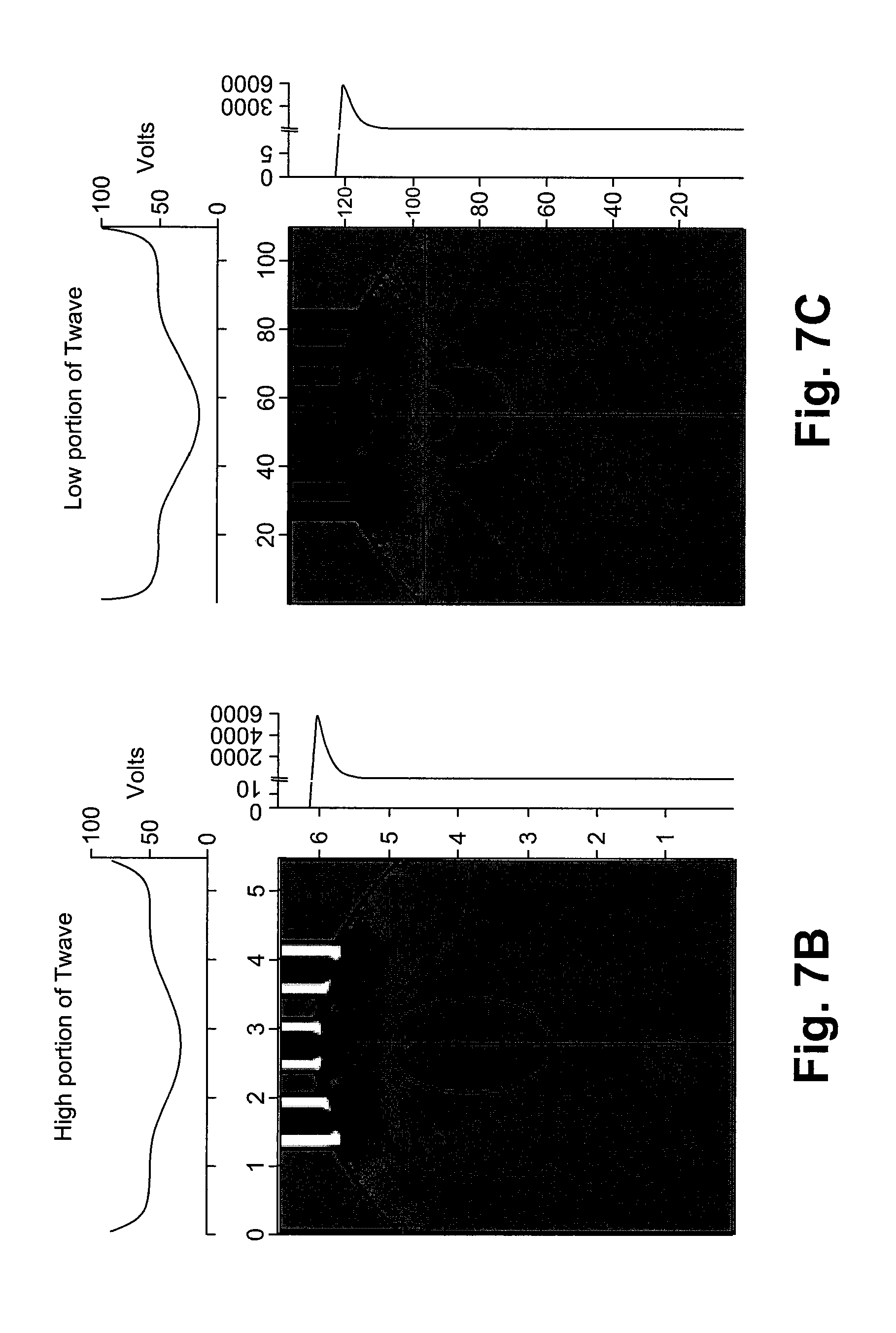
FIG. 7B is a plot showing ion confinement within the device of FIG. 7A at the high portion of a time-dependent electric field.
FIG. 7C is a plot showing ion confinement within the device of FIG. 7A at the low portion of a time-dependent electric field.
FIG. 8 is a plot of ion counts over arrival time of two ions with different mass-to-charge ratios, and separated according to their mobilities, using two different configurations--the embodiment of FIG. 4 or a single board ion mobility separation device and a prior dual board ion mobility separation device.
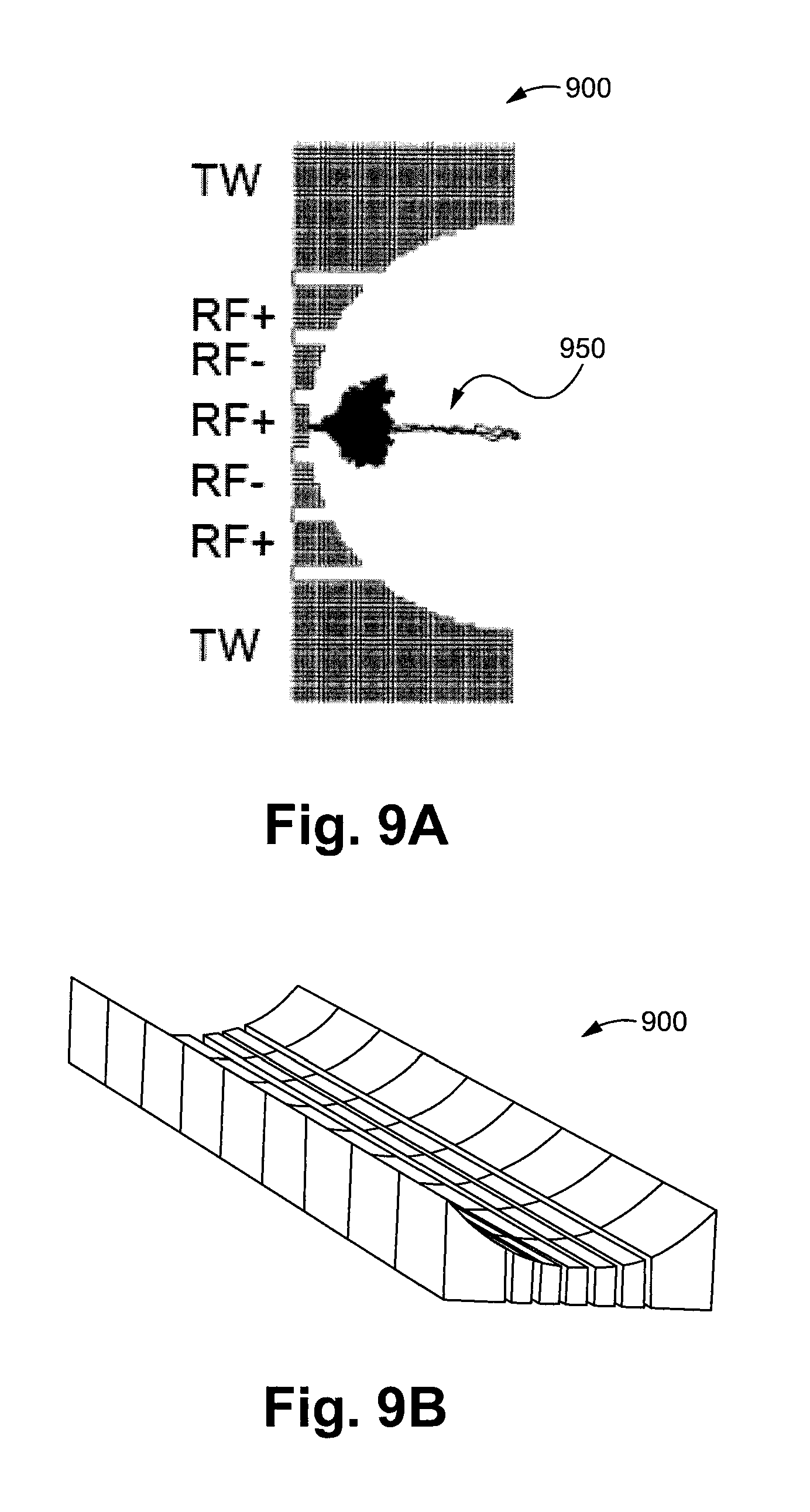
FIGS. 9A and 9B show a cross section and three-dimensional schematic diagram, respectively, of the ion mobility device of FIG. 2, with ions moving through the device at a distance from the surface, with a DC traveling wave field applied to the outside electrodes and opposing phases of RF applied to the inner electrodes, in accordance with one embodiment of the present invention.
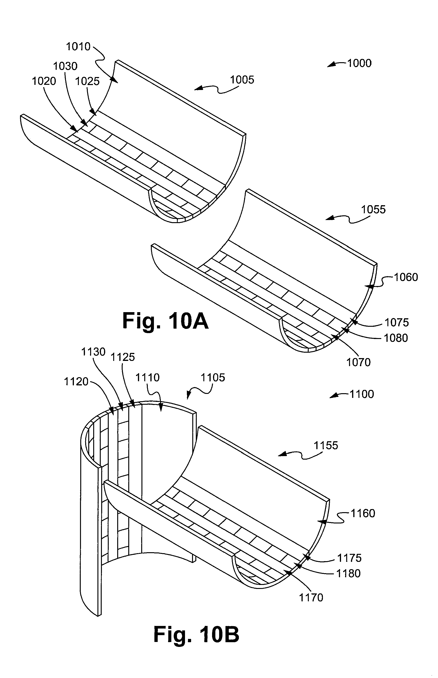
FIG. 10A is a perspective view schematic diagram of two devices, each similar to the embodiment shown in FIGS. 1A-D, with one device above and offset from the other at an angle, to provide a "waterfall" effect of the ions traveling from one device to the other.
FIG. 10B is a perspective view schematic diagram of two devices, each similar to the embodiment shown in FIGS. 1A-D, with the devices positioned orthogonally to one another, to provide a "waterfall" effect of the ions traveling from one device to the other.
DETAILED DESCRIPTION OF THE PREFERRED EMBODIMENTS
The following description includes the preferred best mode of embodiments of the present invention. It will be clear from this description of the invention that the invention is not limited to these illustrated embodiments but that the invention also includes a variety of modifications and embodiments thereto. Therefore the present description should be seen as illustrative and not limiting. While the invention is susceptible of various modifications and alternative constructions, it should be understood, that there is no intention to limit the invention to the specific form disclosed, but, on the contrary, the invention is to cover all modifications, alternative constructions, and equivalents falling within the spirit and scope of the invention as defined in the claims.
Disclosed are methods and devices for ion mobility separations. The device has an open structure and may comprise a drift cell formed by a single surface that is not flat or planar. The single surface is thus open and may be curved or angled to form an ion separation channel and help prevent ion losses, which is in contrast to prior drift cells that have two planar surfaces of electrodes forming the channel.
The single, non-planar surface may be formed by curving a flexible printed circuit board material, by three-dimensional printing, or other means to deposit a conductive material on a non-conductive surface.
A combination of RF and DC fields are applied to arrays of electrodes coupled to the surface to create, along with the shape of the curved surface, confining and driving fields that move ions through the device. Lateral confinement is achievable by a combination of electric fields applied to outer electrodes as well as the curvature of the surface.
In one embodiment, two separate arrays of electrodes positioned closer to the middle of the device confine and drive ions throughout the device.
Ions can be driven through the device either by application of static DC field or time-dependent DC field.
The device allows for ion injection at an angle to the plane of ion motion and construction of, in one example, a helical shaped separation device.
The open, non-planar device, which can be curved, also allows for the following: ion introduction at any location in the device; ion current/mobility/mass measurements, as well as optical measurements, at any location in the device; and the non-planar cross section allows non-rectilinear ion path (e.g. helix) which is not possible with planar devices due to the two top and bottom boards.
The device can also include a cover positioned or disposed on the device. On this cover a voltage can be applied to guard against interfering voltage or potential from, e.g., ground or nearby electronics.
Two or more devices can be combined or coupled together, with one device above and offset from the other at an angle, to provide a "waterfall" effect of the ions traveling from one device to another.
FIGS. 1A-1D show different views of an ion mobility device 100 having a single curved or non-planar surface 105 containing arrays of outer DC electrodes 110 and inner DC electrodes 130. The device 100 also includes arrays of RF electrodes 120 and 125 of opposite phase, RF+ and RF-, on either side of the inner DC electrodes 130, in accordance with one embodiment of the present invention. The arrays are coupled to and extend substantially along the length of the surface 105.
In one embodiment, the DC voltage applied to the outer array DC electrodes 110 is the same. The DC voltages applied to the inner array DC electrodes 130 may be different or may be a DC gradient applied across the inner array 130. The DC voltages or fields may be static DC fields or time-dependent DC fields or waveforms.
As shown in FIG. 1, each inner array of DC electrodes 130 is positioned between an adjacent pair--e.g., adjacent RF arrays 120 and 125 or adjacent RF arrays 125 and 120--of the inner array of RF electrodes. Also, a RF waveform on at least one inner array of RF electrodes 120 and 125 is out of phase with a neighboring or adjacent array of RF electrodes 120 or 125. In one embodiment, an inner RF electrode array 120 or 125 is approximately 180 degrees out of phase or phase shifted with its neighboring inner electrode array 120 or 125 to form a pseudopotential.
The surface 105, which is either curved or non-planar, is a single surface. In one embodiment, the surface 105 is not flat and may be comprised of, but is not limited to, a flexible printed board material.
FIGS. 2A-2D show different views of an ion mobility device 200 having a single curved or non-planar surface 205 containing arrays of outer DC electrodes 210 and arrays of inner RF electrodes 220 and 230 with a superimposed DC field on the inner array of RF electrodes 220 and 230, in accordance with one embodiment of the present invention. The RF field on at least one inner electrode array 220 is out of phase with its neighboring inner electrode 230. For example, the RF waveform phase applied to electrode arrays 220 are positive (+), and the RF waveform phase applied to electrode arrays 230 are negative (-). DC gradient or different voltages are applied to the electrodes 210.
FIGS. 3A-3D show different views of an ion mobility device 300 having a single curved or non-planar surface 305 containing arrays of outer DC electrodes 310 and arrays of inner DC electrodes 330 with different DC fields or a DC gradient applied across the arrays of electrodes 310 and 330. The device 300 also includes arrays of RF electrodes 320 and 325 of opposite phase, RF+ or RF-, on either side of the inner DC electrodes 330, in accordance with one embodiment of the present invention. As such, each inner array of DC electrodes 330 is positioned between an adjacent pair of the inner array of RF electrodes 320 and 325.
The DC field applied to the outer array of DC electrodes 310 is different across the outer array 310 or is a DC gradient. The DC field applied to the inner array of DC electrodes 330 is a DC gradient or is different.
FIGS. 4A-4D show different views of an ion mobility device 400 device having a single curved or non-planar surface 405 containing arrays of inner DC electrodes 430 that are offset or misaligned from the arrays of outer DC electrodes 410. Arrays of RF electrodes 420 and 425 of opposite phase (+ or -) are on either side of the inner DC electrodes 430.
The DC field applied to the outer array of DC electrodes 410 and inner array of DC electrodes 430 is different across the outer and inner DC arrays 410 and 430. In one embodiment, a DC gradient is applied across the outer and inner DC arrays 410 and 430. Each inner array of DC electrodes 430 is positioned between an adjacent pair of the inner array of RF electrodes 420 and 425.
FIG. 5 shows a cross section of the ion mobility device 500 of FIG. 1, with ions 550 moving through the device at a distance from the surface, in accordance with one embodiment of the present invention. The device 500 includes an outer array of DC electrodes 510, an inner array of RF electrodes 520 and 525, and an inner array of DC electrodes 530 positioned between array of RF electrodes 520 and 525 of opposite phase (+ or -).
In the example of FIG. 5, the ions are approximately 0.3 mm from the surface of the device 500. A combination of RF and DC fields applied to the arrays of electrodes 510, 520, 525, and 530, along with the shape of the curved surface, create confining and driving fields that move ions through the device 500. Lateral confinement is achievable by the curved nature of the surface and application of electric fields to the outer electrodes 510. The inner RF and DC electrode arrays 520, 525, and 530 confine and drive ions through the device. The ions can be driven either through a static DC field or a time-dependent DC waveform or field.
FIG. 6 is a plot of ion counts over arrival time using the embodiment of FIG. 1, showing the mobility separation of two ions with different mass-to-charge ratios--m/z 622 and m/z 922.
FIG. 7A is a three-dimensional schematic diagram of the device of FIG. 1, with ions moving through the device at a distance from the surface, in accordance with one embodiment of the present invention.
FIG. 7B is a plot showing ion confinement within the device of FIG. 7A at the high portion of a time-dependent electric field, a dynamic electric field.
FIG. 7C is a plot showing ion confinement within the device of FIG. 7A at the low portion of a time-dependent electric field, a dynamic electric field.
FIG. 8 is a plot of ion counts over arrival time of two ions with different mass-to-charge ratios (m/z 622 and m/z 922) using two different configurations--the embodiment of FIG. 4 or a single board ion mobility separation device and a prior dual board ion mobility separation device. The prior dual boards are straight or planar, while the single board configuration is curved. The length of each device is approximately 76 mm.
FIGS. 9A and 9B show a cross section and three-dimensional schematic diagram, respectively, of the ion mobility device of FIG. 2, with ions moving through the device at a distance from the surface, with a DC traveling wave field applied to the outside electrodes and opposing phases of RF applied to the inner electrodes, in accordance with one embodiment of the present invention.
FIG. 10A is a perspective view schematic diagram of two devices 1005 and 1055 used in combination as an ion mobility separation device or apparatus 1000. Each device 1005 and 1055 is similar to the embodiment shown in FIGS. 1A-D, with one device 1005 above and offset from the other 1055 at an angle, to provide a "waterfall" effect of the ions traveling from one device to the other.
The device 1005 includes outer arrays of DC electrodes 1010, inner arrays of DC electrodes 1030, and arrays of RF electrodes 1020 and 1025. Each inner array of DC electrodes 1030 is positioned between an array of RF electrodes 1020 and 1025 having opposite phases (RF+ or RF-).
The device 1055 includes outer arrays of DC electrodes 1060, inner arrays of DC electrodes 1080, and arrays of RF electrodes 1070 and 1075. Each inner array of DC electrodes 1080 is positioned between an array of RF electrodes 1070 and 1075 having opposite phases (RF+ or RF-).
FIG. 10B is a perspective view schematic diagram of two devices 1105 and 1155 used in combination as an ion mobility separation device or apparatus 1100. Each device 1105 and 1155 is similar to the embodiment shown in FIGS. 1A-D, with the devices 1105 and 1155 positioned orthogonally to one another, to provide a "waterfall" effect of the ions traveling from one device to the other.
The device 1105 includes outer arrays of DC electrodes 1110, inner arrays of DC electrodes 1130, and arrays of RF electrodes 1120 and 1125. Each inner array of DC electrodes 1130 is positioned between an array of RF electrodes 1120 and 1125 having opposite phases (RF+ or RF-).
The device 1155 includes outer arrays of DC electrodes 1160, inner arrays of DC electrodes 1180, and arrays of RF electrodes 1170 and 1175. Each inner array of DC electrodes 1180 is positioned between an array of RF electrodes 1170 and 1175 having opposite phases (RF+ or RF-).
While a number of embodiments of the present invention have been shown and described, it will be apparent to those skilled in the art that many changes and modifications may be made without departing from the invention in its broader aspects. The appended claims, therefore, are intended to cover all such changes and modifications as they fall within the true spirit and scope of the invention.
* * * * *
D00000
D00001
D00002
D00003
D00004
D00005
D00006
D00007
D00008
D00009
D00010
XML
uspto.report is an independent third-party trademark research tool that is not affiliated, endorsed, or sponsored by the United States Patent and Trademark Office (USPTO) or any other governmental organization. The information provided by uspto.report is based on publicly available data at the time of writing and is intended for informational purposes only.
While we strive to provide accurate and up-to-date information, we do not guarantee the accuracy, completeness, reliability, or suitability of the information displayed on this site. The use of this site is at your own risk. Any reliance you place on such information is therefore strictly at your own risk.
All official trademark data, including owner information, should be verified by visiting the official USPTO website at www.uspto.gov. This site is not intended to replace professional legal advice and should not be used as a substitute for consulting with a legal professional who is knowledgeable about trademark law.