Organic electroluminescent materials and devices
Lam , et al. Sept
U.S. patent number 10,418,568 [Application Number 15/147,543] was granted by the patent office on 2019-09-17 for organic electroluminescent materials and devices. This patent grant is currently assigned to Universal Display Corporation. The grantee listed for this patent is Universal Display Corporation. Invention is credited to Raymond Kwong, Siu Tung Lam, Chi Hang Lee, Kit Yee Tsang.


View All Diagrams
| United States Patent | 10,418,568 |
| Lam , et al. | September 17, 2019 |
Organic electroluminescent materials and devices
Abstract
A compound having a structure of Formula I: ##STR00001## is described. In the structure of Formula I, R.sup.A, R.sup.B, and R.sup.C are each independently 5 or 6 membered aryl or heteroaryl rings; R.sup.1, R.sup.2, R.sup.3, and A are selected from a variety of substituents, including being joined or fused to form a ring; A is optionally bonded to at least one benzo or azabenzo ring to form fused rings; X.sup.1 is B, C, N, O, S or Se; and X.sup.2-X.sup.7 are independently B, C or N. Formulations and devices, such as an OLEDs, that include the compound containing a structure of Formula I are also described.
| Inventors: | Lam; Siu Tung (Apleichau, HK), Kwong; Raymond (Fo Tan, HK), Lee; Chi Hang (Chaiwan, HK), Tsang; Kit Yee (Shatin, HK) | ||||||||||
|---|---|---|---|---|---|---|---|---|---|---|---|
| Applicant: |
|
||||||||||
| Assignee: | Universal Display Corporation
(Ewing, NJ) |
||||||||||
| Family ID: | 56137087 | ||||||||||
| Appl. No.: | 15/147,543 | ||||||||||
| Filed: | May 5, 2016 |
Prior Publication Data
| Document Identifier | Publication Date | |
|---|---|---|
| US 20160351811 A1 | Dec 1, 2016 | |
Related U.S. Patent Documents
| Application Number | Filing Date | Patent Number | Issue Date | ||
|---|---|---|---|---|---|
| 62169157 | Jun 1, 2015 | ||||
| Current U.S. Class: | 1/1 |
| Current CPC Class: | C07F 5/022 (20130101); C07F 5/02 (20130101); H01L 51/0071 (20130101); C09K 11/025 (20130101); H01L 51/0085 (20130101); H01L 51/008 (20130101); C09K 11/06 (20130101); H01L 51/0073 (20130101); C07F 5/027 (20130101); C07F 5/05 (20130101); C09K 2211/1007 (20130101); C09K 2211/185 (20130101); C09K 2211/1044 (20130101); H01L 51/5016 (20130101); H01L 51/5012 (20130101) |
| Current International Class: | H01L 51/00 (20060101); C07F 5/02 (20060101); C07F 5/05 (20060101); H01L 51/50 (20060101); C09K 11/02 (20060101); C09K 11/06 (20060101) |
References Cited [Referenced By]
U.S. Patent Documents
| 3392181 | July 1968 | Horn |
| 4769292 | September 1988 | Tang et al. |
| 5061569 | October 1991 | VanSlyke et al. |
| 5247190 | September 1993 | Friend et al. |
| 5703436 | December 1997 | Forrest et al. |
| 5707745 | January 1998 | Forrest et al. |
| 5834893 | November 1998 | Bulovic et al. |
| 5844363 | December 1998 | Gu et al. |
| 6013982 | January 2000 | Thompson et al. |
| 6087196 | July 2000 | Sturm et al. |
| 6091195 | July 2000 | Forrest et al. |
| 6097147 | August 2000 | Baldo et al. |
| 6294398 | September 2001 | Kim et al. |
| 6303238 | October 2001 | Thompson et al. |
| 6337102 | January 2002 | Forrest et al. |
| 6468819 | October 2002 | Kim et al. |
| 6528187 | March 2003 | Okada |
| 6687266 | February 2004 | Ma et al. |
| 6835489 | December 2004 | Kwong et al. |
| 6921915 | July 2005 | Takiguchi et al. |
| 7087321 | August 2006 | Kwong et al. |
| 7090928 | August 2006 | Thompson et al. |
| 7154114 | December 2006 | Brooks et al. |
| 7250226 | July 2007 | Tokito et al. |
| 7279704 | October 2007 | Walters et al. |
| 7332232 | February 2008 | Ma et al. |
| 7338722 | March 2008 | Thompson et al. |
| 7393599 | July 2008 | Thompson et al. |
| 7396596 | July 2008 | Takeuchi et al. |
| 7431968 | October 2008 | Shtein et al. |
| 7445855 | November 2008 | Mackenzie et al. |
| 7534505 | May 2009 | Lin et al. |
| 2002/0034656 | March 2002 | Thompson et al. |
| 2002/0134984 | September 2002 | Igarashi |
| 2002/0158242 | October 2002 | Son et al. |
| 2003/0138657 | July 2003 | Li et al. |
| 2003/0152802 | August 2003 | Tsuboyama et al. |
| 2003/0162053 | August 2003 | Marks et al. |
| 2003/0175553 | September 2003 | Thompson et al. |
| 2003/0230980 | December 2003 | Forrest et al. |
| 2004/0036077 | February 2004 | Ise |
| 2004/0137267 | July 2004 | Igarashi et al. |
| 2004/0137268 | July 2004 | Igarashi et al. |
| 2004/0174116 | September 2004 | Lu et al. |
| 2005/0025993 | February 2005 | Thompson et al. |
| 2005/0112407 | May 2005 | Ogasawara et al. |
| 2005/0238919 | October 2005 | Ogasawara |
| 2005/0244673 | November 2005 | Satoh et al. |
| 2005/0260441 | November 2005 | Thompson et al. |
| 2005/0260447 | November 2005 | Brooks |
| 2005/0260449 | November 2005 | Walters et al. |
| 2006/0008670 | January 2006 | Lin et al. |
| 2006/0202194 | September 2006 | Jeong et al. |
| 2006/0240279 | October 2006 | Adamovich et al. |
| 2006/0251923 | November 2006 | Lin et al. |
| 2006/0263635 | November 2006 | Ise |
| 2006/0280965 | December 2006 | Kwong et al. |
| 2007/0190359 | August 2007 | Knowles et al. |
| 2007/0278938 | December 2007 | Yabunouchi et al. |
| 2008/0015355 | January 2008 | Schafer et al. |
| 2008/0018221 | January 2008 | Egen et al. |
| 2008/0106190 | May 2008 | Yabunouchi et al. |
| 2008/0124572 | May 2008 | Mizuki et al. |
| 2008/0220265 | September 2008 | Xia et al. |
| 2008/0297033 | December 2008 | Knowles et al. |
| 2009/0008605 | January 2009 | Kawamura et al. |
| 2009/0009065 | January 2009 | Nishimura et al. |
| 2009/0017330 | January 2009 | Iwakuma et al. |
| 2009/0030202 | January 2009 | Iwakuma et al. |
| 2009/0039776 | February 2009 | Yamada et al. |
| 2009/0045730 | February 2009 | Nishimura et al. |
| 2009/0045731 | February 2009 | Nishimura et al. |
| 2009/0101870 | April 2009 | Prakash et al. |
| 2009/0108737 | April 2009 | Kwong et al. |
| 2009/0115316 | May 2009 | Zheng et al. |
| 2009/0165846 | July 2009 | Johannes et al. |
| 2009/0167162 | July 2009 | Lin et al. |
| 2009/0179554 | July 2009 | Kuma et al. |
| 2014/0027734 | January 2014 | Kwong |
| 2015/0097162 | April 2015 | Ono |
| 1198372 | Aug 1965 | DE | |||
| 0650955 | May 1995 | EP | |||
| 1725079 | Nov 2006 | EP | |||
| 2034538 | Mar 2009 | EP | |||
| 200511610 | Jan 2005 | JP | |||
| 2007123392 | May 2007 | JP | |||
| 2007254297 | Oct 2007 | JP | |||
| 2008074939 | Apr 2008 | JP | |||
| 01/39234 | May 2001 | WO | |||
| 02/02714 | Jan 2002 | WO | |||
| 02015654 | Feb 2002 | WO | |||
| 03040257 | May 2003 | WO | |||
| 03060956 | Jul 2003 | WO | |||
| 2004093207 | Oct 2004 | WO | |||
| 04107822 | Dec 2004 | WO | |||
| 2005014551 | Feb 2005 | WO | |||
| 2005019373 | Mar 2005 | WO | |||
| 2005030900 | Apr 2005 | WO | |||
| 2005089025 | Sep 2005 | WO | |||
| 2005123873 | Dec 2005 | WO | |||
| 2006009024 | Jan 2006 | WO | |||
| 2006056418 | Jun 2006 | WO | |||
| 2006072002 | Jul 2006 | WO | |||
| 2006082742 | Aug 2006 | WO | |||
| 2006098120 | Sep 2006 | WO | |||
| 2006100298 | Sep 2006 | WO | |||
| 2006103874 | Oct 2006 | WO | |||
| 2006114966 | Nov 2006 | WO | |||
| 2006132173 | Dec 2006 | WO | |||
| 2007002683 | Jan 2007 | WO | |||
| 2007004380 | Jan 2007 | WO | |||
| 2007029798 | Mar 2007 | WO | |||
| 2007063764 | Jun 2007 | WO | |||
| 2007063796 | Jun 2007 | WO | |||
| 2008056746 | May 2008 | WO | |||
| 2008101842 | Aug 2008 | WO | |||
| 2008132085 | Nov 2008 | WO | |||
| 2009000673 | Dec 2008 | WO | |||
| 2009003898 | Jan 2009 | WO | |||
| 2009008311 | Jan 2009 | WO | |||
| 2009018009 | Feb 2009 | WO | |||
| 2009021126 | Feb 2009 | WO | |||
| 2009050290 | Apr 2009 | WO | |||
| 2009062578 | May 2009 | WO | |||
| 2009063833 | May 2009 | WO | |||
| 2009066778 | May 2009 | WO | |||
| 2009066779 | May 2009 | WO | |||
| 2009086028 | Jul 2009 | WO | |||
| 2009100991 | Aug 2009 | WO | |||
| 2012121398 | Sep 2012 | WO | |||
| 2014042197 | Mar 2014 | WO | |||
| 2015053572 | Apr 2015 | WO | |||
Other References
|
Bosdet, Michael J. D. et al., "Blue Fluorescent 4a-Aza-4b-boraphenanthrenes", Organic Letters, 2007, vol. 9, No. 7, pp. 1396-1398. cited by applicant . Demott, Jessica C. et al., "Experimental and computational exploration of the dynamic behavior of (PNP)BF2, a boron compound supported by an amido/bis(phosphine) pincer ligand", Dalton Trans., 2011, 40, pp. 11562-11570. cited by applicant . Hatakeyama, Takuji et al., "Synthess of BN-Fused Polycyclic Aromatics via Tandem Intramolecular Electrophilic Arene Borylation", J. Am. Chem. Soc. 2011, 133, pps. 18614-18617. cited by applicant . Sachdev, Hermann et al., "Structural and Spectroscopic Properties of Aryl Substituted Aminoboranes as Model Compounds and Synthons for B/C/N Materials and New Fluorescent Systems", Z. Anorg. Allg. Chem. 2009, 635, pp. 2112-2119. cited by applicant . Taniguchi, Takuhiro et al., "TICT fluorescence of N-borylated 2,5-diarylpyrroles: a gear like dual motion in the excited state", Dalton Trans., 2013, 42, pp. 620-624. cited by applicant . Wang, Jian et al., "Substituent Effects on Twisted Internal Charge Transfer Excited States of N-Borylated Carbazoles and (Diphenylamino)boranes", J. Phys. Chem. A 2012, 116, pp. 1151-1158. cited by applicant . K. Pilgram and F. Korte, "Uber Die Umsetzung von triarylphosphiten, triarylphosphoniten und triarylboraten mit aromatischen diaminen", Tetrahedron, vol. 19, Issue 1, 1963, pp. 137-141 (English abstract included). cited by applicant . Maya, Leon, "Semiconducting Amorphous Film Containing Carbon Nitrogen and Boron", Journal of The Electrochemical Society, vol. 135, Issue 5, May 1988, pp. 1278-1281. cited by applicant . Extended European Search Report dated Jul. 22, 2016 for corresponding EP Application No. 16171317.7. cited by applicant . Adachi, Chihaya et al., "Organic Electroluminescent Device Having a Hole Conductor as an Emitting Layer," Appl. Phys. Lett., 55(15): 1489-1491 (1989). cited by applicant . Adachi, Chihaya et al., "Nearly 100% Internal Phosphorescence Efficiency in an Organic Light Emitting Device," J. Appl. Phys., 90(10): 5048-5051 (2001). cited by applicant . Adachi, Chihaya et al., "High-Efficierioy Red Electrophosphorescence Devices," Appl. Phys. Lett. 78(11)1622-1624 (2001). cited by applicant . Aonuma, Masaki et al., "Material Design of Hole Transport Materials Capable of Thick-Film Formation in Organic Light Emitting Diodes," Appl. Phys. Lett., Apr. 30, 2007, 90:183503-1-183503-3. cited by applicant . Baldo et al., Highly Efficient Phosphorescent Emission from Organic Electroluminescent Devices, Nature, vol. 395, 151-154, (1998). cited by applicant . Baldo et al., Very high-efficiency green organic light-emitting devices based on electrophosphorescence, Appl. Phys. Lett., vol. 75, No. 1, 4-6 (1999). cited by applicant . Gao, Zhiqiang et al., "Bright-Blue Electroluminescence From a Silyl-Substituted ter-(phenylene-vinylene) derivative," Appl. Phys. Lett., 74(6): 865-867 (1999). cited by applicant . Guo, Tzung-Fang et al., "Highly Efficient Electrophosphorescent Polymer Light-Emitting Devices," Organic Electronics, 1: 15-20 (2000). cited by applicant . Hamada, Yuji et al., "High Luminance in Organic Electroluminescent Devices with Bis(10-hydroxybenzo[h]quinolinato) beryllium as an Emitter," Chem. Lett., 905-906 (1993). cited by applicant . Holmes, R.J. et al., "Blue Organic Electrophosphorescence Using Exothermic Host-Guest Energy Transfer," Appl. Phys. Lett., 82(15):2422-2424 (2003). cited by applicant . Hu, Nan-Xing et al., "Novel High Tg Hole-Transport Molecules Based on Indolo[3,2-b]carbazoles for Organic Light-Emitting Devices," Synthetic Metals, 111-112:421-424 (2000). cited by applicant . Huang, Jinsong et al., "Highly Efficient Red-Emission Polymer Phosphorescent Light-Emitting Diodes Based on Two Novel Tris(1-phenylisoquinolinato-C2,N)iridium(III) Derivatives," Adv. Mater., 19:739-743 (2007). cited by applicant . Huang, Wei-Sheng et al., "Highly Phosphorescent Bis-Cyclometalated Indium Complexes Containing Benzoimidazole-Based Ligands," Chem. Mater., 16(12):2480-2488 (2004). cited by applicant . Hung, L.S. et al., "Anode Modification in Organic Light-Emitting Diodes by Low-Frequency Plasma Polymerization of CHF3," Appl. Phys. Lett., 78(5):673-675 (2001). cited by applicant . Ikai, Masamichi et al., "Highly Efficient Phosphorescence From Organic Light-Emitting Devices with an Exciton-Block Layer," Appl. Phys. Lett., 79(2):156-158 (2001). cited by applicant . Ikeda, Hisao et al., "P-185 Low-Drive-Voltage OLEDs with a Buffer Layer Having Molybdenum Oxide," SID Symposium Digest, 37:923-926 (2006). cited by applicant . Inada, Hiroshi and Shirota, Yasuhiko, "1,3,5-Tris[4-(diphenylamino)phenyl]benzene and its Methylsubstituted Derivatives as a Novel Class of Amorphous Molecular Materials," J. Mater. Chem., 3(3):319-320 (1993). cited by applicant . Kanno, Hiroshi et al., "Highly Efficient and Stable Red Phosphorescent Organic Light-Emitting Device Using bis[2-(2-benzothiazoyl)phenolato]zinc(II) as host material," Appl. Phys. Lett., 90:123509-1-123509-3 (2007). cited by applicant . Kido, Junji et al., 1,2,4-Triazole Derivative as an Electron Transport Layer in Organic Electroluminescent Devices, Jpn. J. Appl. Phys., 32:L917-L920 (1993). cited by applicant . Kuwabara, Yoshiyuki et al., "Thermally Stable Muitilayered Organic Electroluminescent Devices Using Novel Starburst Molecules, 4,4',4''-Tri(N-carbazolyl)triphenylamine (TCTA) and 4,4',4''-Tris(3-methylphenylphenyl-amino) triphenylamine (m-MTDATA), as Hole-Transpont Materials," Adv. Mater., 6(9):677-679 (1994). cited by applicant . Kwong, Raymond C. et al., "High Operational Stability of Electrophospherescent Devices," Appl. Phys. Lett., 81(1) 162-164 (2002). cited by applicant . Lamansky, Sergey et al., "Synthesis and Characterization of Phosphorescent Cyclometalated Iridium Complexes," Inorg. Chem., 40(7):1704-1711 (2001). cited by applicant . Lee, Chang-Lyoul et al., "Polymer Phosphorescent Light-Emitting Devices Doped with Tris(2-phenylpyridine) Iridium as a Triplet Emitter," Appl. Phys. Lett., 77(15):2280-2282 (2000). cited by applicant . Lo, Shih-Chun et al., "Blue Phosphorescence from Iridium(III) Complexes at Room Temperature," Chem. Mater., 18(21)5119-5129 (2006). cited by applicant . Ma, Yuguang et al., "Triplet Luminescent Dinuclear-Gold(l) Complex-Based Light-Emitting Diodes with Low Turn-On voltage," Appl. Phys. Lett. 74(10):1361-1353 (1999). cited by applicant . Mi, Bao-Xiu et al., "Thermally Stable Hole-Transporting Material for Organic Light-Emitting Diode an Isoindole Derivative," Chem. Mater., 15(16):3148-3151 (2003). cited by applicant . Nishida, Jun-ichi et al., "Preparation, Characterization, and Electroluminescence Characteristics of .alpha.-Diimine-type Platinum(II) Complexes with Perfluorinated Phenyl Groups as Ligands," Chem. Lett., 34(4): 592-593 (2005). cited by applicant . Niu, Yu-Hua et al., "Highly Efficient Electrophosphorescent Devices with Saturated Red Emission from a Neutral Osmium Complex," Chem. Mater., 17(13):3532-3536 (2005). cited by applicant . Noda, Tetsuya and Shirota, Yasuhiko, "5,5'-Bis(dimesitylboryl)-2,2'-bithiophene and 5,5'-Bis(dimesitylboryl)-2,2'5',2''-terthiophene as a Novel Family of Electron-Transporting Amorphous Molecular Materials," J. Am. Chem. Soc., 120 (37):9714-9716 (1998). cited by applicant . Okumoto, Kenji et al., "Green Fluorescent Organic Light-Emitting Device with External Quantum Efficiency of Nearly 10%," Appl. Phys. Lett., 89:063504-1-063504-3 (2006). cited by applicant . Palilis, Leonidas C., "High Efflciency Molecular Organic Light-Emitting Diodes Based on Silole Derivatives and Their Exciplexes," Organic Electronics, 4:113-121 (2003). cited by applicant . Paulose, Betty Marie Jennifer S. et al., "First Examples of Alkenyl Pyridines as Organic Ligands for Phosphorescent Iridium Complexes," Adv. Mater., 16(22):2003-2007 (2004). cited by applicant . Ranjan, Sudhir et al., "Realizing Green Phosphorescent Light-Emitting Materials from Rhenium(I) Pyrazolato Diimine Complexes," Inorg. Chem., 42(4):1248-1255 (2003). cited by applicant . Sakamoto, Youichi et al., "Synthesis, Characterization, and Electron-Transport Property of Perfluorinated Phenylene Dendrimers," J. Am. Chem. Soc., 122(8):1832-1833 (2000). cited by applicant . Salbeck J. et al., "Low Molecular Organic Gasses for Blue Electroluminescence," Synthetic Metals, 91: 209-215 (1997). cited by applicant . Shirota, Yasuhiko et al., "Starburst Molecules Based on pi-Electron Systems as Materials for Organic Electroluminescent Devices," Journal of Luminescence, 72-74:985-991 (1997). cited by applicant . Sotoyama, Wataru et al., "Efficient Organic Light-Emitting Diodes with Phosphorescent Platinum Complexes Containing N C N-Coordinating Tridentate Ligand," Appl. Phys. Lett., 86:153505-1-153505-3 (2005). cited by applicant . Sun, Yiru and Forrest, Stephen R., "High-Efficiency White Organic Light Emitting Devices with Three Separate Phosphorescent Emission Layers," Appl. Phys. Lett., 91:263503-1-263503-3 (2007). cited by applicant . T. Osterg{hacek over (a)}rd et al., "Langmuir-Blodgett Light-Emitting Diodes of Poly(3-Hexylthiophene) Electro-Optical Characteristics Related to Structure," Synthetic Metals, 88:171-177 (1997). cited by applicant . Takizawa, Shin-ya et al., "Phosphorescent Iridium Complexes Based on 2-Phenylimidazo[1,2- .alpha.]pyridine Ligands Tuning of Emission Color toward the Blue Region and Application to Polymer Light-Emitting Devices," Inorg. Chem., 46(10):4308-4319 (2007). cited by applicant . Tang, C.W. and VanSlyke, S.A., "Organic Electroluminescent Diodes," Appl. Phys. Lett., 51(12):913-915 (1987). cited by applicant . Tung, Yung-Liang et al., "Organic Light-Emitting Diodes Based on Charge-Neutral Ru II PHosphorescent Emitters," Adv. Mater., 17(8)1059-1064 (2005). cited by applicant . Van Slyke, S. A. et al., "Organic Electroluminescent Devices with Improved Stability," Appl. Phys. Lett., 69(15):2160-2162 (1996). cited by applicant . Wang, Y. et al., "Highly Efficient Electroluminescent Materials Based on Fluorinated Organometallic Iridium Compounds," Appl. Phys. Lett., 79(4):449-451 (2001). cited by applicant . Wong, Keith Man-Chung et al., A Novel Class of Phosphorescent Gold(III) Alkynyl-Based Organic Light-Emitting Devices with Tunable Colour, Chem. Commun., 2906-2908 (2005). cited by applicant . Wong, Wai-Yeung, "Multifunctional Iridium Complexes Based on Carbazole Modules as Highly Efficient Electrophosphors," Agnew. Chem. Int. Ed., 45:7800-7803 (2006). cited by applicant. |
Primary Examiner: Barton; Jeffrey T
Assistant Examiner: Sun; Michael Y
Attorney, Agent or Firm: Duane Morris LLP
Claims
We claim:
1. A compound having a structure of Formula I: ##STR00127## wherein R.sup.A, R.sup.B, and R.sup.C are each independently 5 or 6 membered aryl or heteroaryl rings; wherein R.sup.1, R.sup.2, and R.sup.3 each independently represent no substitutions or up to the maximum available substitutions; wherein R.sup.1, R.sup.2, and R.sup.3 are each independently selected from the group consisting of hydrogen, deuterium, halide, alkyl, cycloalkyl, heteroalkyl, arylalkyl, alkoxy, aryloxy, amino, silyl, alkenyl, cycloalkenyl, heteroalkenyl, alkynyl, aryl, heteroaryl, acyl, carbonyl, carboxylic acids, ester, nitrile, isonitrile, sulfanyl, sulfinyl, sulfonyl, phosphine, a substituent of Formula I, and combinations thereof; wherein any adjacent R.sup.1, R.sup.2, and R.sup.3 are optionally joined or fused to form a ring; wherein A is selected from the group consisting of halide, alkyl, cycloalkyl, heteroalkyl, arylalkyl, alkoxy, aryloxy, amino, silyl, alkenyl, cycloalkenyl, heteroalkenyl, alkynyl, aryl, heteroaryl, acyl, carbonyl, carboxylic acids, ester, nitrile, isonitrile, sulfanyl, sulfinyl, sulfonyl, phosphine, a substituent of Formula I, partially or fully deuterated variants thereof, and combinations thereof; wherein A is optionally bonded to at least one benzo or azabenzo ring to form fused rings; wherein X.sup.1 is B, C, N, O, S or Se; and wherein X.sup.2-X.sup.7 are independently B, C or N.
2. The compound of claim 1, wherein A is aryl or heteroaryl.
3. The compound of claim 1, wherein A is selected from the group consisting of phenyl, carbazole, azacarbazole, dibenzofuran, dibenzothiophene, dibenzoselenophene, azadibenzofuran, azadibenzothiophene, azadibenzoselenophene, triphenylene, azatriphenylene, and combinations thereof; wherein A is optionally further substituted by one or more substituent B; wherein B is selected from the group consisting of hydrogen, deuterium, halide, alkyl, cycloalkyl, heteroalkyl, arylalkyl, alkoxy, aryloxy, amino, silyl, alkenyl, cycloalkenyl, heteroalkenyl, alkynyl, aryl, heteroaryl, acyl, carbonyl, carboxylic acids, ester, nitrile, isonitrile, sulfanyl, sulfinyl, sulfonyl, phosphine, and combinations thereof; and wherein B is optionally bonded to at least one benzo or azabenzo ring to form a fused ring.
4. The compound of claim 3, wherein the compound is selected from the group consisting of: ##STR00128## ##STR00129## ##STR00130## ##STR00131## ##STR00132## ##STR00133## ##STR00134## ##STR00135## ##STR00136## ##STR00137## ##STR00138## ##STR00139## ##STR00140## ##STR00141## ##STR00142## ##STR00143## ##STR00144## ##STR00145## ##STR00146## ##STR00147## ##STR00148## ##STR00149## ##STR00150## ##STR00151## ##STR00152## ##STR00153##
5. The compound of claim 1, wherein X.sup.1 is C or N, A is aryl or heteroaryl and A is connected to X.sup.1 to form a fused ring.
6. The compound of claim 5, wherein the compound is selected from the group consisting of: ##STR00154## ##STR00155## ##STR00156## ##STR00157## ##STR00158## ##STR00159## ##STR00160## ##STR00161## ##STR00162## ##STR00163## ##STR00164## ##STR00165## ##STR00166## ##STR00167## ##STR00168## ##STR00169## ##STR00170## ##STR00171## ##STR00172## ##STR00173## ##STR00174## ##STR00175## ##STR00176## ##STR00177## ##STR00178## ##STR00179## ##STR00180## ##STR00181## ##STR00182##
7. The compound of claim 1, wherein R.sup.A is an aryl ring.
8. The compound of claim 1, wherein R.sup.B is an aryl ring or a heteroaryl ring comprising one hetero-atom selected from the group consisting of N, O, and S.
9. The compound of claim 1, wherein R.sup.C is an aryl ring or a heteroaryl ring comprising one or two nitrogen atoms.
10. The compound of claim 1, wherein: (a) at least one R.sup.1, R.sup.2, or R.sup.3 comprises a substituent selected from the group consisting of carbazole, azacarbazole, dibenzofuran, azadibenzofuran, dibenzothiophene, azadibenzothiophene, dibenzoselenophene, azadibenzoselenophene, triphenylene, azatriphenylene, diphenyl(silyl), triphenyl(silyl), and tetraphenyl(silyl); (b) two adjacent substituents of R.sup.1, R.sup.2, or R.sup.3 form a fused benzo substituent on R.sup.A, R.sup.B, or R.sup.C, respectively; or (c) both option (a) and option (b) are true.
11. The compound of claim 1, wherein at least one R.sup.1, R.sup.2, or R.sup.3 comprises a substituent selected from the group consisting of carbazole, azacarbazole, dibenzofuran, azadibenzofuran, dibenzothiophene, azadibenzothiophene, dibenzoselenophene, azadibenzoselenophene, triphenylene, azatriphenylene, diphenyl(silyl), triphenyl(silyl), and tetraphenyl(silyl); and the remaining substituents R.sup.1, R.sup.2, and R.sup.3 are H.
12. The compound of claim 1, wherein X.sup.1-X.sup.6 are C, and X.sup.7 is C or N.
13. A first organic light-emitting device comprising: an anode; a cathode; and an organic layer, disposed between the anode and the cathode, comprising a compound having a structure of Formula I: ##STR00183## wherein R.sup.A, R.sup.B, and R.sup.C are each independently 5 or 6 membered aryl or heteroaryl rings; wherein R.sup.1, R.sup.2, and R.sup.3 each independently represent no substitutions or up to the maximum available substitutions; wherein R.sup.1, R.sup.2, and R.sup.3 are each independently selected from the group consisting of hydrogen, deuterium, halide, alkyl, cycloalkyl, heteroalkyl, arylalkyl, alkoxy, aryloxy, amino, silyl, alkenyl, cycloalkenyl, heteroalkenyl, alkynyl, aryl, heteroaryl, acyl, carbonyl, carboxylic acids, ester, nitrile, isonitrile, sulfanyl, sulfinyl, sulfonyl, phosphine, a substituent of Formula I, and combinations thereof; wherein any adjacent R.sup.1, R.sup.2, and R.sup.3 are optionally joined or fused to form a ring; wherein A is selected from the group consisting of halide, alkyl, cycloalkyl, heteroalkyl, arylalkyl, alkoxy, aryloxy, amino, silyl, alkenyl, cycloalkenyl, heteroalkenyl, alkynyl, aryl, heteroaryl, acyl, carbonyl, carboxylic acids, ester, nitrile, isonitrile, sulfanyl, sulfinyl, sulfonyl, phosphine, a substituent of Formula I, partially or fully deuterated variations thereof, and combinations thereof; wherein A is optionally bonded to at least one benzo or azabenzo ring to form fused rings; wherein X.sup.1 is B, C, N, O, S or Se; and wherein X.sup.2-X.sup.7 are independently B, C or N.
14. The first device of claim 13, wherein the organic layer is an emissive layer and the compound is a host.
15. The first device of claim 13, wherein the organic layer further comprises an emissive dopant.
16. The first device of claim 15, wherein the emissive dopant is a transition metal complex having at least one ligand or part of the ligand, if the ligand is more than bidentate, selected from the group consisting of: ##STR00184## ##STR00185## wherein each X.sup.1 to X.sup.13 are independently selected from the group consisting of carbon and nitrogen; wherein X is selected from the group consisting of BR', NR', PR', O, S, Se, C.dbd.O, S.dbd.O, SO.sub.2, CR'R'', SiR'R'', and GeR'R''; wherein R' and R'' are optionally fused or joined to form a ring; wherein each R.sub.a, R.sub.b, R.sub.c, and R.sub.d may represent from mono substitution to the possible maximum number of substitutions, or no substitution; wherein R', R'', R.sub.a, R.sub.b, R.sub.c, and R.sub.d are each independently selected from the group consisting of hydrogen, deuterium, halide, alkyl, cycloalkyl, heteroalkyl, arylalkyl, alkoxy, aryloxy, amino, silyl, alkenyl, cycloalkenyl, heteroalkenyl, alkynyl, aryl, heteroaryl, acyl, carbonyl, carboxylic acids, ester, nitrile, isonitrile, sulfanyl, sulfinyl, sulfonyl, phosphino, and combinations thereof; and wherein any two adjacent substituents of R.sub.a, R.sub.b, R.sub.c, and R.sub.d are optionally fused or joined to form a ring or form a multidentate ligand.
17. The first device of claim 13, wherein (i) the organic layer is a charge carrier blocking layer and the compound is a charge carrier blocking material in the organic layer, or (ii) the organic layer is an charge carrier transporting layer and the compound is a charge carrier transporting material in the organic layer.
18. The first device of claim 13, wherein the first device is incorporated into a device selected from the group consisting of a consumer product, an electronic component module, an organic light-emitting device, and a lighting panel.
19. A formulation comprising a compound and one or more components selected from the group consisting of a solvent, a host, a hole injection material, hole transport material, and an electron transport layer material, wherein the compound has a structure of Formula I: ##STR00186## wherein R.sup.A, R.sup.B, and R.sup.C are each independently 5 or 6 membered aryl or heteroaryl rings; wherein R.sup.1, R.sup.2, and R.sup.3 each independently represent no substitutions or up to the maximum available substitutions; wherein R.sup.1, R.sup.2, and R.sup.3 are each independently selected from the group consisting of hydrogen, deuterium, halide, alkyl, cycloalkyl, heteroalkyl, arylalkyl, alkoxy, aryloxy, amino, silyl, alkenyl, cycloalkenyl, heteroalkenyl, alkynyl, aryl, heteroaryl, acyl, carbonyl, carboxylic acids, ester, nitrile, isonitrile, sulfanyl, sulfinyl, sulfonyl, phosphine, a substituent of Formula I, and combinations thereof; wherein any adjacent R.sup.1, R.sup.2, and R.sup.3 are optionally joined or fused to form a ring; wherein A is selected from the group consisting of halide, alkyl, cycloalkyl, heteroalkyl, arylalkyl, alkoxy, aryloxy, amino, silyl, alkenyl, cycloalkenyl, heteroalkenyl, alkynyl, aryl, heteroaryl, acyl, carbonyl, carboxylic acids, ester, nitrile, isonitrile, sulfanyl, sulfinyl, sulfonyl, phosphine, a substituent of Formula I, partially or fully deuterated variations thereof, and combinations thereof; wherein A is optionally bonded to at least one benzo or azabenzo ring to form fused rings; wherein X.sup.1 is B, C, N, O, S or Se; and wherein X.sup.2-X.sup.7 are independently B, C or N.
20. The compound of claim 1, A is not connected to X.sup.1 to form a fused ring.
Description
CROSS-REFERENCE TO RELATED APPLICATIONS
This application is a non-provisional of U.S. Patent Application Ser. No. 62/169,157, filed Jun. 1, 2015, the entire contents of which are incorporated herein by reference.
PARTIES TO A JOINT RESEARCH AGREEMENT
The claimed invention was made by, on behalf of, and/or in connection with one or more of the following parties to a joint university corporation research agreement: The Regents of the University of Michigan, Princeton University, University of Southern California, and the Universal Display Corporation. The agreement was in effect on and before the date the claimed invention was made, and the claimed invention was made as a result of activities undertaken within the scope of the agreement.
FIELD
The present invention relates to compounds for use as electroluminescent materials, such as hosts, and devices, such as organic light emitting diodes, including the same.
BACKGROUND
Opto-electronic devices that make use of organic materials are becoming increasingly desirable for a number of reasons. Many of the materials used to make such devices are relatively inexpensive, so organic opto-electronic devices have the potential for cost advantages over inorganic devices. In addition, the inherent properties of organic materials, such as their flexibility, may make them well suited for particular applications such as fabrication on a flexible substrate. Examples of organic opto-electronic devices include organic light emitting diodes/devices (OLEDs), organic phototransistors, organic photovoltaic cells, and organic photodetectors. For OLEDs, the organic materials may have performance advantages over conventional materials. For example, the wavelength at which an organic emissive layer emits light may generally be readily tuned with appropriate dopants.
OLEDs make use of thin organic films that emit light when voltage is applied across the device. OLEDs are becoming an increasingly interesting technology for use in applications such as flat panel displays, illumination, and backlighting. Several OLED materials and configurations are described in U.S. Pat. Nos. 5,844,363, 6,303,238, and 5,707,745, which are incorporated herein by reference in their entirety.
One application for phosphorescent emissive molecules is a full color display. Industry standards for such a display call for pixels adapted to emit particular colors, referred to as "saturated" colors. In particular, these standards call for saturated red, green, and blue pixels. Alternatively the OLED can be designed to emit white light. In conventional liquid crystal displays emission from a white backlight is filtered using absorption filters to produce red, green and blue emission. The same technique can also be used with OLEDs. The white OLED can be either a single EML device or a stack structure. Color may be measured using CIE coordinates, which are well known to the art.
One example of a green emissive molecule is tris(2-phenylpyridine) iridium, denoted Ir(ppy).sub.3, which has the following structure:
##STR00002##
In this, and later figures herein, we depict the dative bond from nitrogen to metal (here, Ir) as a straight line.
As used herein, the term "organic" includes polymeric materials as well as small molecule organic materials that may be used to fabricate organic opto-electronic devices. "Small molecule" refers to any organic material that is not a polymer, and "small molecules" may actually be quite large. Small molecules may include repeat units in some circumstances. For example, using a long chain alkyl group as a substituent does not remove a molecule from the "small molecule" class. Small molecules may also be incorporated into polymers, for example as a pendent group on a polymer backbone or as a part of the backbone. Small molecules may also serve as the core moiety of a dendrimer, which consists of a series of chemical shells built on the core moiety. The core moiety of a dendrimer may be a fluorescent or phosphorescent small molecule emitter. A dendrimer may be a "small molecule." and it is believed that all dendrimers currently used in the field of OLEDs are small molecules.
As used herein, "top" means furthest away from the substrate, while "bottom" means closest to the substrate. Where a first layer is described as "disposed over" a second layer, the first layer is disposed further away from substrate. There may be other layers between the first and second layer, unless it is specified that the first layer is "in contact with" the second layer. For example, a cathode may be described as "disposed over" an anode, even though there are various organic layers in between.
As used herein, "solution processable" means capable of being dissolved, dispersed, or transported in and/or deposited from a liquid medium, either in solution or suspension form.
A ligand may be referred to as "photoactive" when it is believed that the ligand directly contributes to the photoactive properties of an emissive material. A ligand may be referred to as "ancillary" when it is believed that the ligand does not contribute to the photoactive properties of an emissive material, although an ancillary ligand may alter the properties of a photoactive ligand.
As used herein, and as would be generally understood by one skilled in the art, a first "Highest Occupied Molecular Orbital" (HOMO) or "Lowest Unoccupied Molecular Orbital" (LUMO) energy level is "greater than" or "higher than" a second HOMO or LUMO energy level if the first energy level is closer to the vacuum energy level. Since ionization potentials (IP) are measured as a negative energy relative to a vacuum level, a higher HOMO energy level corresponds to an IP having a smaller absolute value (an IP that is less negative). Similarly, a higher LUMO energy level corresponds to an electron affinity (EA) having a smaller absolute value (an EA that is less negative). On a conventional energy level diagram, with the vacuum level at the top, the LUMO energy level of a material is higher than the HOMO energy level of the same material. A "higher" HOMO or LUMO energy level appears closer to the top of such a diagram than a "lower" HOMO or LUMO energy level.
As used herein, and as would be generally understood by one skilled in the art, a first work function is "greater than" or "higher than" a second work function if the first work function has a higher absolute value. Because work functions are generally measured as negative numbers relative to vacuum level, this means that a "higher" work function is more negative. On a conventional energy level diagram, with the vacuum level at the top, a "higher" work function is illustrated as further away from the vacuum level in the downward direction. Thus, the definitions of HOMO and LUMO energy levels follow a different convention than work functions.
More details on OLEDs, and the definitions described above, can be found in U.S. Pat. No. 7,279,704, which is incorporated herein by reference in its entirety.
SUMMARY
According to an embodiment, a compound is provided that has the structure of Formula I:
##STR00003## is described. In the structure of Formula I:
R.sup.A, R.sup.B, and R.sup.C are each independently 5 or 6 membered aryl or heteroaryl rings;
R.sup.1, R.sup.2, and R.sup.3 each independently represent no substitutions or up to the maximum available substitutions:
R.sup.1, R.sup.2, and R.sup.3 are each independently selected from the group consisting of hydrogen, deuterium, halide, alkyl, cycloalkyl, heteroalkyl, arylalkyl, alkoxy, aryloxy, amino, silyl, alkenyl, cycloalkenyl, heteroalkenyl, alkynyl, aryl, heteroaryl, acyl, carbonyl, carboxylic acids, ester, nitrile, isonitrile, sulfanyl, sulfinyl, sulfonyl, phosphine, a substituent of Formula I, and combinations thereof:
any adjacent R.sup.1, R.sup.2, and R.sup.3 are optionally joined or fused to form a ring;
A is selected from the group consisting of hydrogen, deuterium halide, alkyl, cycloalkyl, heteroalkyl, arylalkyl, alkoxy, aryloxy, amino, silyl, alkenyl, cycloalkenyl, heteroalkenyl, alkynyl, aryl, heteroaryl, acyl, carbonyl, carboxylic acids, ester, nitrile, isonitrile, sulfanyl, sulfinyl, sulfonyl, phosphine, a substituent of Formula I, and combinations thereof;
A is optionally bonded to at least one benzo or azabenzo ring to form fused rings;
X.sup.1 is B, C, N, O, S or Se; and
X.sup.2-X.sup.7 are independently B, C or N.
According to another embodiment, an organic light emitting diode/device (OLED) is also provided. The OLED can include an anode, a cathode, and an organic layer, disposed between the anode and the cathode. The organic layer can include a compound comprising a structure of Formula I. According to yet another embodiment, the organic light emitting device is incorporated into a device selected from a consumer product, an electronic component module, and/or a lighting panel.
According to yet another embodiment, a formulation containing a compound comprising a structure of Formula I is provided.
BRIEF DESCRIPTION OF THE DRAWINGS
FIG. 1 shows an organic light emitting device.
FIG. 2 shows an inverted organic light emitting device that does not have a separate electron transport layer.
DETAILED DESCRIPTION
Generally, an OLED comprises at least one organic layer disposed between and electrically connected to an anode and a cathode. When a current is applied, the anode injects holes and the cathode injects electrons into the organic layer(s). The injected holes and electrons each migrate toward the oppositely charged electrode. When an electron and hole localize on the same molecule, an "exciton," which is a localized electron-hole pair having an excited energy state, is formed. Light is emitted when the exciton relaxes via a photoemissive mechanism. In some cases, the exciton may be localized on an excimer or an exciplex. Non-radiative mechanisms, such as thermal relaxation, may also occur, but are generally considered undesirable.
The initial OLEDs used emissive molecules that emitted light from their singlet states ("fluorescence") as disclosed, for example, in U.S. Pat. No. 4,769,292, which is incorporated by reference in its entirety. Fluorescent emission generally occurs in a time frame of less than 10 nanoseconds.
More recently, OLEDs having emissive materials that emit light from triplet states ("phosphorescence") have been demonstrated. Baldo et al., "Highly Efficient Phosphorescent Emission from Organic Electroluminescent Devices," Nature, vol. 395, 151-154, 1998; ("Baldo-I") and Baldo et al., "Very high-efficiency green organic light-emitting devices based on electrophosphorescence," Appl. Phys. Lett., vol. 75. No. 3, 4-6 (1999) ("Baldo-II"), are incorporated by reference in their entireties. Phosphorescence is described in more detail in U.S. Pat. No. 7,279,704 at cols. 5-6, which are incorporated by reference.
FIG. 1 shows an organic light emitting device 100. The figures are not necessarily drawn to scale. Device 100 may include a substrate 110, an anode 115, a hole injection layer 120, a hole transport layer 125, an electron blocking layer 130, an emissive layer 135, a hole blocking layer 140, an electron transport layer 145, an electron injection layer 150, a protective layer 155, a cathode 160, and a barrier layer 170. Cathode 160 is a compound cathode having a first conductive layer 162 and a second conductive layer 164. Device 100 may be fabricated by depositing the layers described, in order. The properties and functions of these various layers, as well as example materials, are described in more detail in U.S. Pat. No. 7,279,704 at cols. 6-10, which are incorporated by reference.
More examples for each of these layers are available. For example, a flexible and transparent substrate-anode combination is disclosed in U.S. Pat. No. 5,844,363, which is incorporated by reference in its entirety. An example of a p-doped hole transport layer is m-MTDATA doped with F.sub.4-TCNQ at a molar ratio of 50:1, as disclosed in U.S. Patent Application Publication No. 2003/0230980, which is incorporated by reference in its entirety. Examples of emissive and host materials are disclosed in U.S. Pat. No. 6,303,238 to Thompson et al., which is incorporated by reference in its entirety. An example of an n-doped electron transport layer is BPhen doped with Li at a molar ratio of 1:1, as disclosed in U.S. Patent Application Publication No. 2003/0230980, which is incorporated by reference in its entirety. U.S. Pat. Nos. 5,703,436 and 5,707,745, which are incorporated by reference in their entireties, disclose examples of cathodes including compound cathodes having a thin layer of metal such as Mg:Ag with an overlying transparent, electrically-conductive, sputter-deposited ITO layer. The theory and use of blocking layers is described in more detail in U.S. Pat. No. 6,097,147 and U.S. Patent Application Publication No. 2003/0230980, which are incorporated by reference in their entireties. Examples of injection layers are provided in U.S. Patent Application Publication No. 2004/0174116, which is incorporated by reference in its entirety. A description of protective layers may be found in U.S. Patent Application Publication No. 2004/0174116, which is incorporated by reference in its entirety.
FIG. 2 shows an inverted OLED 200. The device includes a substrate 210, a cathode 215, an emissive layer 220, a hole transport layer 225, and an anode 230. Device 200 may be fabricated by depositing the layers described, in order. Because the most common OLED configuration has a cathode disposed over the anode, and device 200 has cathode 215 disposed under anode 230, device 200 may be referred to as an "inverted" OLED. Materials similar to those described with respect to device 100 may be used in the corresponding layers of device 200. FIG. 2 provides one example of how some layers may be omitted from the structure of device 100.
The simple layered structure illustrated in FIGS. 1 and 2 is provided by way of non-limiting example, and it is understood that embodiments of the invention may be used in connection with a wide variety of other structures. The specific materials and structures described are exemplary in nature, and other materials and structures may be used. Functional OLEDs may be achieved by combining the various layers described in different ways, or layers may be omitted entirely, based on design, performance, and cost factors. Other layers not specifically described may also be included. Materials other than those specifically described may be used. Although many of the examples provided herein describe various layers as comprising a single material, it is understood that combinations of materials, such as a mixture of host and dopant, or more generally a mixture, may be used. Also, the layers may have various sublayers. The names given to the various layers herein are not intended to be strictly limiting. For example, in device 200, hole transport layer 225 transports holes and injects holes into emissive layer 220, and may be described as a hole transport layer or a hole injection layer. In one embodiment, an OLED may be described as having an "organic layer" disposed between a cathode and an anode. This organic layer may comprise a single layer, or may further comprise multiple layers of different organic materials as described, for example, with respect to FIGS. 1 and 2.
Structures and materials not specifically described may also be used, such as OLEDs comprised of polymeric materials (PLEDs) such as disclosed in U.S. Pat. No. 5,247,190 to Friend et al., which is incorporated by reference in its entirety. By way of further example, OLEDs having a single organic layer may be used. OLEDs may be stacked, for example as described in U.S. Pat. No. 5,707,745 to Forrest et al, which is incorporated by reference in its entirety. The OLED structure may deviate from the simple layered structure illustrated in FIGS. 1 and 2. For example, the substrate may include an angled reflective surface to improve out-coupling, such as a mesa structure as described in U.S. Pat. No. 6,091,195 to Forrest et al., and/or a pit structure as described in U.S. Pat. No. 5,834,893 to Bulovic et al., which are incorporated by reference in their entireties.
Unless otherwise specified, any of the layers of the various embodiments may be deposited by any suitable method. For the organic layers, preferred methods include thermal evaporation, ink-jet, such as described in U.S. Pat. Nos. 6,013,982 and 6,087,196, which are incorporated by reference in their entireties, organic vapor phase deposition (OVPD), such as described in U.S. Pat. No. 6,337,102 to Forrest et al., which is incorporated by reference in its entirety, and deposition by organic vapor jet printing (OVJP), such as described in U.S. Pat. No. 7,431,968, which is incorporated by reference in its entirety. Other suitable deposition methods include spin coating and other solution based processes. Solution based processes are preferably carried out in nitrogen or an inert atmosphere. For the other layers, preferred methods include thermal evaporation. Preferred patterning methods include deposition through a mask, cold welding such as described in U.S. Pat. Nos. 6,294,398 and 6,468,819, which are incorporated by reference in their entireties, and patterning associated with some of the deposition methods such as ink-jet and OVJD. Other methods may also be used. The materials to be deposited may be modified to make them compatible with a particular deposition method. For example, substituents such as alkyl and aryl groups, branched or unbranched, and preferably containing at least 3 carbons, may be used in small molecules to enhance their ability to undergo solution processing. Substituents having 20 carbons or more may be used, and 3-20 carbons is a preferred range. Materials with asymmetric structures may have better solution processability than those having symmetric structures, because asymmetric materials may have a lower tendency to recrystallize. Dendrimer substituents may be used to enhance the ability of small molecules to undergo solution processing.
Devices fabricated in accordance with embodiments of the present invention may further optionally comprise a barrier layer. One purpose of the barrier layer is to protect the electrodes and organic layers from damaging exposure to harmful species in the environment including moisture, vapor and/or gases, etc. The barrier layer may be deposited over, under or next to a substrate, an electrode, or over any other parts of a device including an edge. The barrier layer may comprise a single layer, or multiple layers. The barrier layer may be formed by various known chemical vapor deposition techniques and may include compositions having a single phase as well as compositions having multiple phases. Any suitable material or combination of materials may be used for the barrier layer. The barrier layer may incorporate an inorganic or an organic compound or both. The preferred barrier layer comprises a mixture of a polymeric material and a non-polymeric material as described in U.S. Pat. No. 7,968,146, PCT Pat. Application Nos. PCT/US2007/023098 and PCT/US2009/042829, which are herein incorporated by reference in their entireties. To be considered a "mixture", the aforesaid polymeric and non-polymeric materials comprising the barrier layer should be deposited under the same reaction conditions and/or at the same time. The weight ratio of polymeric to non-polymeric material may be in the range of 95:5 to 5:95. The polymeric material and the non-polymeric material may be created from the same precursor material. In one example, the mixture of a polymeric material and a non-polymeric material consists essentially of polymeric silicon and inorganic silicon.
Devices fabricated in accordance with embodiments of the invention can be incorporated into a wide variety of electronic component modules (or units) that can be incorporated into a variety of electronic products or intermediate components. Examples of such electronic products or intermediate components include display screens, lighting devices such as discrete light source devices or lighting panels, etc. that can be utilized by the end-user product manufacturers. Such electronic component modules can optionally include the driving electronics and/or power source(s). Devices fabricated in accordance with embodiments of the invention can be incorporated into a wide variety of consumer products that have one or more of the electronic component modules (or units) incorporated therein. Such consumer products would include any kind of products that include one or more light source(s) and/or one or more of some type of visual displays. Some examples of such consumer products include flat panel displays, computer monitors, medical monitors, televisions, billboards, lights for interior or exterior illumination and/or signaling, heads-up displays, fully or partially transparent displays, flexible displays, laser printers, telephones, cell phones, tablets, phablets, personal digital assistants (PDAs), wearable device, laptop computers, digital cameras, camcorders, viewfinders, micro-displays, 3-D displays, vehicles, a large area wall, theater or stadium screen, or a sign. Various control mechanisms may be used to control devices fabricated in accordance with the present invention, including passive matrix and active matrix. Many of the devices are intended for use in a temperature range comfortable to humans, such as 18 degrees C. to 30 degrees C., and more preferably at room temperature (20-25 degrees C.), but could be used outside this temperature range, for example, from -40 degree C. to +80 degree C.
The materials and structures described herein may have applications in devices other than OLEDs. For example, other optoelectronic devices such as organic solar cells and organic photodetectors may employ the materials and structures. More generally, organic devices, such as organic transistors, may employ the materials and structures.
The term "halo," "halogen," or "halide" as used herein includes fluorine, chlorine, bromine, and iodine.
The term "alkyl" as used herein contemplates both straight and branched chain alkyl radicals. Preferred alkyl groups are those containing from one to fifteen carbon atoms and includes methyl, ethyl, propyl, 1-methylethyl, butyl, 1-methylpropyl, 2-methylpropyl, pentyl, 1-methylbutyl, 2-methylbutyl, 3-methylbutyl, 1,1-dimethylpropyl, 1,2-dimethylpropyl, 2,2-dimethylpropyl, and the like. Additionally, the alkyl group may be optionally substituted.
The term "cycloalkyl" as used herein contemplates cyclic alkyl radicals. Preferred cycloalkyl groups are those containing 3 to 10 ring carbon atoms and includes cyclopropyl, cyclopentyl, cyclohexyl, adamantyl, and the like. Additionally, the cycloalkyl group may be optionally substituted.
The term "alkenyl" as used herein contemplates both straight and branched chain alkene radicals. Preferred alkenyl groups are those containing two to fifteen carbon atoms. Additionally, the alkenyl group may be optionally substituted.
The term "alkynyl" as used herein contemplates both straight and branched chain alkyne radicals. Preferred alkynyl groups are those containing two to fifteen carbon atoms. Additionally, the alkynyl group may be optionally substituted.
The terms "aralkyl" or "arylalkyl" as used herein are used interchangeably and contemplate an alkyl group that has as a substituent an aromatic group. Additionally, the aralkyl group may be optionally substituted.
The term "heterocyclic group" as used herein contemplates aromatic and non-aromatic cyclic radicals. Hetero-aromatic cyclic radicals also means heteroaryl. Preferred hetero-non-aromatic cyclic groups are those containing 3 to 7 ring atoms which includes at least one hetero atom, and includes cyclic amines such as morpholino, piperdino, pyrrolidino, and the like, and cyclic ethers, such as tetrahydrofuran, tetrahydropyran, and the like. Additionally, the heterocyclic group may be optionally substituted.
The term "aryl" or "aromatic group" as used herein contemplates single-ring groups and polycyclic ring systems. The polycyclic rings may have two or more rings in which two carbons are common to two adjoining rings (the rings are "fused") wherein at least one of the rings is aromatic. e.g., the other rings can be cycloalkyls, cycloalkenyls, aryl, heterocycles, and/or heteroaryls. Preferred aryl groups are those containing six to thirty carbon atoms, preferably six to twenty carbon atoms, more preferably six to twelve carbon atoms. Especially preferred is an aryl group having six carbons, ten carbons or twelve carbons. Suitable aryl groups include phenyl, biphenyl, triphenyl, triphenylene, tetraphenylene, naphthalene, anthracene, phenalene, phenanthrene, fluorene, pyrene, chrysene, perylene, and azulene, preferably phenyl, biphenyl, triphenyl, triphenylene, fluorene, and naphthalene. Additionally, the aryl group may be optionally substituted.
The term "heteroaryl" as used herein contemplates single-ring hetero-aromatic groups that may include from one to five heteroatoms. The term heteroaryl also includes polycyclic hetero-aromatic systems having two or more rings in which two atoms are common to two adjoining rings (the rings are "fused") wherein at least one of the rings is a heteroaryl, e.g., the other rings can be cycloalkyls, cycloalkenyls, aryl, heterocycles, and/or heteroaryls. Preferred heteroaryl groups are those containing three to thirty carbon atoms, preferably three to twenty carbon atoms, more preferably three to twelve carbon atoms. Suitable heteroaryl groups include dibenzothiophene, dibenzofuran, dibenzoselenophene, furan, thiophene, benzofuran, benzothiophene, benzoselenophene, carbazole, indolocarbazole, pyridylindole, pyrrolodipyridine, pyrazole, imidazole, triazole, oxazole, thiazole, oxadiazole, oxatriazole, dioxazole, thiadiazole, pyridine, pyridazine, pyrimidine, pyrazine, triazine, oxazine, oxathiazine, oxadiazine, indole, benzimidazole, indazole, indoxazine, benzoxazole, benzisoxazole, benzothiazole, quinoline, isoquinoline, cinnoline, quinazoline, quinoxaline, naphthyridine, phthalazine, pteridine, xanthene, acridine, phenazine, phenothiazine, phenoxazine, benzofuropyridine, furodipyridine, benzothienopyridine, thienodipyridine, benzoselenophenopyridine, and selenophenodipyridine, preferably dibenzothiophene, dibenzofuran, dibenzoselenophene, carbazole, indolocarbazole, imidazole, pyridine, triazine, benzimidazole, 1,2-azaborine, 1,3-azaborine, 1,4-azaborine, borazine, and aza-analogs thereof. Additionally, the heteroaryl group may be optionally substituted.
The alkyl, cycloalkyl, alkenyl, alkynyl, aralkyl, heterocyclic group, aryl, and heteroaryl may be optionally substituted with one or more substituents selected from the group consisting of hydrogen, deuterium, halogen, alkyl, cycloalkyl, heteroalkvl, arylalkyl, alkoxy, aryloxy, amino, cyclic amino, silyl, alkenyl, cycloalkenyl, heteroalkenyl, alkynyl, aryl, heteroaryl, acyl, carbonyl, carboxylic acid, ether, ester, nitrile, isonitrile, sulfanyl, sulfinyl, sulfonyl, phosphino, and combinations thereof.
As used herein, "substituted" indicates that a substituent other than H is bonded to the relevant position, such as carbon. Thus, for example, where R.sup.1 is mono-substituted, then one R.sup.1 must be other than H. Similarly, where R.sup.1 is di-substituted, then two of R.sup.1 must be other than H. Similarly, where R.sup.1 is unsubstituted, R.sup.1 is hydrogen for all available positions.
The "aza" designation in the fragments described herein, i.e. aza-dibenzofuran, aza-dibenzothiophene, etc. means that one or more of the C--H groups in the respective fragment can be replaced by a nitrogen atom, for example, and without any limitation, azatriphenylene encompasses both dibenzo[f,h]quinoxaline and dibenzo[f,h]quinoline. One of ordinary skill in the art can readily envision other nitrogen analogs of the aza-derivatives described above, and all such analogs are intended to be encompassed by the terms as set forth herein.
It is to be understood that when a molecular fragment is described as being a substituent or otherwise attached to another moiety, its name may be written as if it were a fragment (e.g. phenyl, phenylene, naphthyl, dibenzofuryl) or as if it were the whole molecule (e.g. benzene, naphthalene, dibenzofuran). As used herein, these different ways of designating a substituent or attached fragment are considered to be equivalent.
High triplet hosts are important to providing good device efficiency for blue and green phosphorescent OLEDs. Azaborine containing hosts may be beneficial since the B--N linkage may increase the triplet energy without losing the aromatic character which is important to stabilization of charge.
According to one embodiment, a compound having a structure of Formula I:
##STR00004## is described. In the structure of Formula I:
R.sup.A, R.sup.B, and R.sup.C are each independently 5 or 6 membered aryl or heteroaryl rings;
R.sup.1, R.sup.2, and R.sup.3 each independently represent no substitutions or up to the maximum available substitutions:
R.sup.1, R.sup.2, and R.sup.3 are each independently selected from the group consisting of hydrogen, deuterium, halide, alkyl, cycloalkyl, heteroalkyl, arylalkyl, alkoxy, aryloxy, amino, silyl, alkenyl, cycloalkenyl, heteroalkenyl, alkynyl, aryl, heteroaryl, acyl, carbonyl, carboxylic acids, ester, nitrile, isonitrile, sulfanyl, sulfinyl, sulfonyl, phosphine, a substituent of Formula I, and combinations thereof:
wherein any adjacent R.sup.1, R.sup.2, and R.sup.3 are optionally joined or fused to form a ring;
A is selected from the group consisting of hydrogen, deuterium, halide, alkyl, cycloalkyl, heteroalkyl, arylalkyl, alkoxy, aryloxy, amino, silyl, alkenyl, cycloalkenyl, heteroalkenyl, alkynyl, aryl, heteroaryl, acyl, carbonyl, carboxylic acids, ester, nitrile, isonitrile, sulfanyl, sulfinyl, sulfonyl, phosphine, a substituent of Formula I, and combinations thereof;
A is optionally bonded to at least one benzo or azabenzo ring to form fused rings;
X.sup.1 is B, C, N, O, S or Se; and
X.sup.2-X.sup.7 are independently B, C or N.
In some embodiments, the compound is a dimer. In some embodiments, any R.sup.1, R.sup.2, and R.sup.3 substituents are optionally joined or fused to form a 5- or 6-membered ring, which may be further substituted based on the definition of R.sup.1, R.sup.2, and R.sup.3.
In some embodiments, X.sup.1-X.sup.6 are C, and X.sup.7 is C or N.
In some embodiments, A is aryl or heteroaryl. In some embodiments, A is selected from the group consisting of phenyl, carbazole, azacarbazole, dibenzofuran, dibenzothiophene, dibenzoselenophene, azadibenzofuran, azadibenzothiophene, azadibenzoselenophene, triphenylene, azatriphenylene, and combinations thereof, and A is optionally further substituted by one or more substituent B. In such embodiments, B is selected from the group consisting of hydrogen, deuterium, halide, alkyl, cycloalkyl, heteroalkyl, arylalkyl, alkoxy, aryloxy, amino, silyl, alkenyl, cycloalkenyl, heteroalkenyl, alkynyl, aryl, heteroaryl, acyl, carbonyl, carboxylic acids, ester, nitrile, isonitrile, sulfanyl, sulfinyl, sulfonyl, phosphine, and combinations thereof; and B is optionally bonded to at least one benzo or azabenzo ring to form a fused ring.
In some embodiments, the compound is selected from the group consisting of:
##STR00005## ##STR00006## ##STR00007## ##STR00008## ##STR00009## ##STR00010## ##STR00011## ##STR00012## ##STR00013## ##STR00014## ##STR00015## ##STR00016## ##STR00017## ##STR00018## ##STR00019## ##STR00020## ##STR00021## ##STR00022## ##STR00023## ##STR00024## ##STR00025## ##STR00026## ##STR00027## ##STR00028##
In some embodiments, X.sup.1 is C or N, A is aryl or heteroaryl and A is connected to X.sup.1 to form a fused ring. In some such embodiments, the compound is selected from the group consisting of:
##STR00029## ##STR00030## ##STR00031## ##STR00032## ##STR00033## ##STR00034## ##STR00035## ##STR00036## ##STR00037## ##STR00038## ##STR00039## ##STR00040## ##STR00041## ##STR00042## ##STR00043## ##STR00044## ##STR00045## ##STR00046## ##STR00047## ##STR00048## ##STR00049## ##STR00050## ##STR00051## ##STR00052## ##STR00053## ##STR00054##
In some embodiments, R.sup.A is an aryl ring. In some embodiments, R.sup.A is benzene.
In some embodiments, R.sup.B is an aryl ring or a heteroaryl ring comprising one hetero-atom selected from the group consisting of N, O, and S. In some embodiments, R.sup.B is selected from the group consisting of benzene, pyridine, furan, thiophene.
In some embodiments, R.sup.C is an aryl ring or a heteroaryl ring comprising one or two nitrogen atoms. In some embodiments, R.sup.C is selected from the group consisting of benzene, pyridine, imidazole.
In some embodiments, (a) at least one R.sup.1, R.sup.2, or R.sup.3 comprises a substituent selected from the group consisting of carbazole, azacarbazole, dibenzofuran, azadibenzofuran, dibenzothiophene, azadibenzothiophene, dibenzoselenophene, azadibenzoselenophene, triphenylene, azatriphenylene, diphenyl(silyl), triphenyl(silyl), and tetraphenyl(silyl); (b) two adjacent substituents of R.sup.1, R.sup.2, or R.sup.3 form a fused benzo substituent on R.sup.A, R.sup.B, or R.sup.C, respectively; or (c) both option (a) and option (b) are true.
In some embodiments, at least one R.sup.1, R.sup.2, or R.sup.3 comprises a substituent selected from the group consisting of carbazole, azacarbazole, dibenzofuran, azadibenzofuran, dibenzothiophene, azadibenzothiophene, dibenzoselenophene, azadibenzoselenophene, triphenylene, azatriphenylene, diphenyl(silyl), triphenyl(silyl), and tetraphenyl(silyl); and the remaining substituents R.sup.1, R.sup.2, and R.sup.3 are H. In some embodiments, exactly one R.sup.1, R.sup.2, or R.sup.3 comprises a substituent selected from the group consisting of carbazole, azacarbazole, dibenzofuran, azadibenzofuran, dibenzothiophene, azadibenzothiophene, dibenzoselenophene, azadibenzoselenophene, triphenylene, azatriphenylene, diphenyl(silyl), triphenyl(silyl), and tetraphenyl(silyl); and the remaining substituents R.sup.1, R.sup.2, and R.sup.3 are H.
In some embodiments, exactly one R.sup.1 comprises a substituent selected from the group consisting of carbazole, azacarbazole, dibenzofuran, azadibenzofuran, dibenzothiophene, azadibenzothiophene, dibenzoselenophene, azadibenzoselenophene, triphenylene, azatriphenylene, diphenyl(silyl), triphenyl(silyl), and tetraphenyl(silyl); and the remaining substituents R.sup.1, R.sup.2, and R.sup.3 are H. In some embodiments, exactly one R.sup.2 comprises a substituent selected from the group consisting of carbazole, azacarbazole, dibenzofuran, azadibenzofuran, dibenzothiophene, azadibenzothiophene, dibenzoselenophene, azadibenzoselenophene, triphenylene, azatriphenylene, diphenyl(silyl), triphenyl(silyl), and tetraphenyl(silyl); and the remaining substituents R.sup.1, R.sup.2, and R.sup.3 are H. In some embodiments, exactly one R.sup.3 comprises a substituent selected from the group consisting of carbazole, azacarbazole, dibenzofuran, azadibenzofuran, dibenzothiophene, azadibenzothiophene, dibenzoselenophene, azadibenzoselenophene, triphenylene, azatriphenylene, diphenyl(silyl), triphenyl(silyl), and tetraphenyl(silyl); and the remaining substituents R.sup.1, R.sup.2, and R.sup.3 are H.
According to another embodiment, an OLED is described. The OLED includes an anode; a cathode; and an organic layer, disposed between the anode and the cathode. In such embodiments, the organic layer includes a compound having a structure of Formula I, and its variations described herein. In some embodiments, the organic layer is an emissive layer and the compound is a host.
In some embodiments, the OLED is incorporated into a device selected from the group consisting of a consumer product, an electronic component module, and a lighting panel.
In some embodiments, the organic layer further comprises an emissive dopant. The emissive dopant can be a phosphorescent dopant and/or a fluorescent dopant. In some such embodiments, the emissive dopant is a transition metal complex having at least one ligand or part of the ligand, if the ligand is more than bidentate, selected from the group consisting of:
##STR00055## ##STR00056## In the emissive dopant ligand structure:
each X.sup.1 to X.sup.13 is independently selected from the group consisting of carbon and nitrogen;
X is selected from the group consisting of BR', NR', PR', O, S, Se, C.dbd.O, S.dbd.O, SO.sub.2, CR'R'', SiR'R'', and GeR'R'';
R' and R'' are optionally fused or joined to form a ring;
each R.sub.a, R.sub.b, R.sub.c, and R.sub.d may represent from mono substitution to the possible maximum number of substitutions, or no substitution;
R', R'', R.sub.a, R.sub.b, R.sub.c, and R.sub.d are each independently selected from the group consisting of hydrogen, deuterium, halide, alkyl, cycloalkyl, heteroalkyl, arylalkyl, alkoxy, aryloxy, amino, silyl, alkenyl, cycloalkenyl, heteroalkenyl, alkynyl, aryl, heteroaryl, acyl, carbonyl, carboxylic acids, ester, nitrile, isonitrile, sulfanyl, sulfinyl, sulfonyl, phosphino, and combinations thereof; and
any two adjacent substituents of R.sub.a, R.sub.b, R.sub.c, and R.sub.d are optionally fused or joined to form a ring or form a multidentate ligand.
In some embodiments, the organic layer is a charge carrier blocking layer and the compound is a charge carrier blocking material in the organic layer. In some embodiments, the organic layer is an charge carrier transporting layer and the compound is a charge carrier transporting material in the organic layer.
In another embodiment, a formulation comprising a compound having a structure of Formula I and its variations described herein is disclosed. The formulation can include one or more components selected from the group consisting of a solvent, a host, a hole injection material, hole transport material, and an electron transport layer material, disclosed herein.
Combination with Other Materials
The materials described herein as useful for a particular layer in an organic light emitting device may be used in combination with a wide variety of other materials present in the device. For example, emissive dopants disclosed herein may be used in conjunction with a wide variety of hosts, transport layers, blocking layers, injection layers, electrodes and other layers that may be present. The materials described or referred to below are non-limiting examples of materials that may be useful in combination with the compounds disclosed herein, and one of skill in the art can readily consult the literature to identify other materials that may be useful in combination.
Conductivity Dopants:
A charge transport layer can be doped with conductivity dopants to substantially alter its density of charge carriers, which will in turn alter its conductivity. The conductivity is increased by generating charge carriers in the matrix material, and depending on the type of dopant, a change in the Fermi level of the semiconductor may also be achieved. Hole-transporting layer can be doped by p-type conductivity dopants and n-type conductivity dopants are used in the electron-transporting layer.
Non-limiting examples of the conductivity dopants that may be used in an OLED in combination with materials disclosed herein are exemplified below together with references that disclose those materials: EP01617493, EP01968131, EP2020694, EP2684932, US20050139810, US20070160905, US20090167167, US2010288362, WO06081780, WO2009003455, WO2009008277, WO2009011327, WO2014009310, US2007252140, US2015060804 and US2012146012.
##STR00057## ##STR00058## ##STR00059## HIL/HTL:
A hole injecting/transporting material to be used in the present invention is not particularly limited, and any compound may be used as long as the compound is typically used as a hole injecting/transporting material. Examples of the material include, but are not limited to: a phthalocyanine or porphyrin derivative; an aromatic amine derivative; an indolocarbazole derivative; a polymer containing fluorohydrocarbon; a polymer with conductivity dopants; a conducting polymer, such as PEDOT/PSS; a self-assembly monomer derived from compounds such as phosphonic acid and silane derivatives; a metal oxide derivative, such as MoO.sub.x; a p-type semiconducting organic compound, such as 1,4,5,8,9,12-Hexaazatriphenylenehexacarbonitrile; a metal complex, and a cross-linkable compounds.
Examples of aromatic amine derivatives used in HIL or HTL include, but are not limited to the following general structures:
##STR00060##
Each of Ar.sup.1 to Ar.sup.9 is selected from the group consisting of aromatic hydrocarbon cyclic compounds such as benzene, biphenyl, triphenyl, triphenylene, naphthalene, anthracene, phenalene, phenanthrene, fluorene, pyrene, chrysene, perylene, and azulene; the group consisting of aromatic heterocyclic compounds such as dibenzothiophene, dibenzofuran, dibenzoselenophene, furan, thiophene, benzofuran, benzothiophene, benzoselenophene, carbazole, indolocarbazole, pyridylindole, pyrrolodipyridine, pyrazole, imidazole, triazole, oxazole, thiazole, oxadiazole, oxatriazole, dioxazole, thiadiazole, pyridine, pyridazine, pyrimidine, pyrazine, triazine, oxazine, oxathiazine, oxadiazine, indole, benzimidazole, indazole, indoxazine, benzoxazole, benzisoxazole, benzothiazole, quinoline, isoquinoline, cinnoline, quinazoline, quinoxaline, naphthyridine, phthalazine, pteridine, xanthene, acridine, phenazine, phenothiazine, phenoxazine, benzofuropyridine, furodipyridine, benzothienopyridine, thienodipyridine, benzoselenophenopyridine, and selenophenodipyridine; and the group consisting of 2 to 10 cyclic structural units which are groups of the same type or different types selected from the aromatic hydrocarbon cyclic group and the aromatic heterocyclic group and are bonded to each other directly or via at least one of oxygen atom, nitrogen atom, sulfur atom, silicon atom, phosphorus atom, boron atom, chain structural unit and the aliphatic cyclic group. Each Ar may be unsubstituted or may be substituted by a substituent selected from the group consisting of deuterium, halide, alkyl, cycloalkyl, heteroalkyl, arylalkyl, alkoxy, aryloxy, amino, silyl, alkenyl, cycloalkenyl, heteroalkenyl, alkynyl, aryl, heteroaryl, acyl, carbonyl, carboxylic acids, ester, nitrile, isonitrile, sulfanyl, sulfinyl, sulfonyl, phosphino, and combinations thereof.
In one aspect, Ar.sup.1 to Ar.sup.9 is independently selected from the group consisting of:
##STR00061## wherein k is an integer from 1 to 20; X.sup.101 to X.sup.108 is C (including CH) or N; Z.sup.101 is NAr.sup.1, O, or S; Ar.sup.1 has the same group defined above.
Examples of metal complexes used in HIL or HTL include, but are not limited to the following general formula:
##STR00062## wherein Met is a metal, which can have an atomic weight greater than 40; (Y.sup.101-Y.sup.102) is a bidentate ligand, Y.sup.101 and Y.sup.102 are independently selected from C, N, O, P, and S; L.sup.101 is an ancillary ligand; k' is an integer value from 1 to the maximum number of ligands that may be attached to the metal; and k'+k'' is the maximum number of ligands that may be attached to the metal.
In one aspect, (Y.sup.101-Y.sup.102) is a 2-phenylpyridine derivative. In another aspect, (Y.sup.101-Y.sup.102) is a carbene ligand. In another aspect, Met is selected from Ir, Pt, Os, and Zn. In a further aspect, the metal complex has a smallest oxidation potential in solution vs. Fc.sup.+/Fc couple less than about 0.6 V.
Non-limiting examples of the HIL and HTL materials that may be used in an OLED in combination with materials disclosed herein are exemplified below together with references that disclose those materials: CN102702075, DE 102012005215, EP01624500, EP01698613, EP01806334, EP01930964, EP01972613, EP01997799, EP02011790. EP02055700, EP02055701, EP1725079, EP2085382, EP2660300, EP650955, JP07-073529, JP2005112765, JP2007091719, JP2008021687, JP2014-009196, KR20110088898, KR20130077473, TW201139402, U.S. Ser. No. 06/517,957, US20020158242, US20030162053, US20050123751, US20060182993, US20060240279, US20070145888, US20070181874, US20070278938, US20080014464, US20080091025, US20080106190. US20080124572, US20080145707, US20080220265, US20080233434, US20080303417, US2008107919. US20090115320, US20090167161, US2009066235, US2011007385, US20110163302, US2011240968, US2011278551. US2012205642, US2013241401, US20140117329, US2014183517, U.S. Pat. Nos. 5,061,569, 5,639,914, WO05075451, WO07125714, WO08023550, WO08023759, WO2009145016, WO2010061824, WO2011075644, WO2012177006, WO2013018530, WO2013039073, WO2013087142, WO2013118812, WO2013120577, WO2013157367, WO2013175747, WO2014002873, WO2014015935, WO2014015937, WO2014030872, WO2014030921, WO2014034791, WO2014104514, WO2014157018.
##STR00063## ##STR00064## ##STR00065## ##STR00066## ##STR00067## ##STR00068## ##STR00069## ##STR00070## ##STR00071## ##STR00072## ##STR00073## ##STR00074## ##STR00075## EBL:
An electron blocking layer (EBL) may be used to reduce the number of electrons and/or excitons that leave the emissive layer. The presence of such a blocking layer in a device may result in substantially higher efficiencies, and or longer lifetime, as compared to a similar device lacking a blocking layer. Also, a blocking layer may be used to confine emission to a desired region of an OLED. In some embodiments, the EBL material has a higher LUMO (closer to the vacuum level) and/or higher triplet energy than the emitter closest to the EBL interface. In some embodiments, the EBL material has a higher LUMO (closer to the vacuum level) and or higher triplet energy than one or more of the hosts closest to the EBL interface. In one aspect, the compound used in EBL contains the same molecule or the same functional groups used as one of the hosts described below.
Additional Hosts:
The light emitting layer of the organic EL device of the present invention preferably contains at least a metal complex as light emitting dopant material, and may contain one or more additional host materials using the metal complex as a dopant material. Examples of the host material are not particularly limited, and any metal complexes or organic compounds may be used as long as the triplet energy of the host is larger than that of the dopant. Any host material may be used with any dopant so long as the triplet criteria is satisfied.
Examples of metal complexes used as host are preferred to have the following general formula:
##STR00076## wherein Met is a metal; (Y.sup.103-Y.sup.104) is a bidentate ligand, Y.sup.103 and Y.sup.104 are independently selected from C, N, O, P, and S; L.sup.101 is an another ligand; k' is an integer value from 1 to the maximum number of ligands that may be attached to the metal; and k'+k'' is the maximum number of ligands that may be attached to the metal.
In one aspect, the metal complexes are:
##STR00077## wherein (O--N) is a bidentate ligand, having metal coordinated to atoms O and N.
In another aspect, Met is selected from Ir and Pt. In a further aspect, (Y.sup.103-Y.sup.104) is a carbene ligand.
Examples of other organic compounds used as additional host are selected from the group consisting of aromatic hydrocarbon cyclic compounds such as benzene, biphenyl, triphenyl, triphenylene, naphthalene, anthracene, phenalene, phenanthrene, fluorene, pyrene, chrysene, perylene, azulene; group consisting aromatic heterocyclic compounds such as dibenzothiophene, dibenzofuran, dibenzoselenophene, furan, thiophene, benzofuran, benzothiophene, benzoselenophene, carbazole, indolocarbazole, pyridylindole, pyrrolodipyridine, pyrazole, imidazole, triazole, oxazole, thiazole, oxadiazole, oxatriazole, dioxazole, thiadiazole, pyridine, pyridazine, pyrimidine, pyrazine, triazine, oxazine, oxathiazine, oxadiazine, indole, benzimidazole, indazole, indoxazine, benzoxazole, benzisoxazole, benzothiazole, quinoline, isoquinoline, cinnoline, quinazoline, quinoxaline, naphthyridine, phthalazine, pteridine, xanthene, acridine, phenazine, phenothiazine, phenoxazine, benzofuropyridine, furodipyridine, benzothienopyridine, thienodipyridine, benzoselenophenopyridine, and selenophenodipyridine; and group consisting 2 to 10 cyclic structural units which are groups of the same type or different types selected from the aromatic hydrocarbon cyclic group and the aromatic heterocyclic group and are bonded to each other directly or via at least one of oxygen atom, nitrogen atom, sulfur atom, silicon atom, phosphorus atom, boron atom, chain structural unit and the aliphatic cyclic group. Wherein each group is further substituted by a substituent selected from the group consisting of hydrogen, deuterium, halide, alkyl, cycloalkyl, heteroalkyl, arylalkyl, alkoxy, arvloxy, amino, silyl, alkenyl, cycloalkenyl, heteroalkenyl, alkynyl, aryl, heteroaryl, acyl, carbonyl, carboxylic acids, ester, nitrile, isonitrile, sulfanyl, sulfinyl, sulfonyl, phosphino, and combinations thereof.
In one aspect, host compound contains at least one of the following groups in the molecule:
##STR00078## ##STR00079## wherein R.sup.101 to R.sup.107 is independently selected from the group consisting of hydrogen, deuterium, halide, alkyl, cycloalkyl, heteroalkyl, arylalkyl, alkoxy, aryloxy, amino, silyl, alkenyl, cycloalkenyl, heteroalkenyl, alkynyl, aryl, heteroaryl, acyl, carbonyl, carboxylic acids, ester, nitrile, isonitrile, sulfanyl, sulfinyl, sulfonyl, phosphino, and combinations thereof, when it is aryl or heteroaryl, it has the similar definition as Ar's mentioned above. k is an integer from 0 to 20 or 1 to 20. k''' is an integer from 0 to 20. X.sup.101 to X.sup.108 is selected from C (including CH) or N. Z.sup.101 and Z.sup.102 is selected from NR.sup.101, O, or S. Non-limiting examples of the additional host materials that may be used in an OLED in combination with the host compound disclosed herein are exemplified below together with references that disclose those materials: EP2034538, EP2034538A, EP2757608, JP2007254297, KR20100079458, KR20120088644, KR20120129733, KR20130115564. TW201329200, US20030175553, US20050238919, US20060280965, US20090017330, US20090030202, US20090167162, US20090302743, US20090309488, US20100012931, US20100084966, US20100187984, US2010187984, US2012075273. US2012126221, US2013009543, US2013105787, US2013175519, US2014001446, US20140183503, US20140225088, US2014034914, U.S. Pat. No. 7,154,114, WO2001039234, WO2004093207. WO2005014551, WO2005089025, WO2006072002, WO2006114966, WO2007063754, WO2008056746, WO2009003898, WO2009021126, WO2009063833, WO2009066778. WO2009066779, WO2009086028, WO2010056066, WO2010107244, WO2011081423, WO2011081431, WO2011086863, WO2012128298, WO2012133644, WO2012133649, WO2013024872, WO2013035275, WO2013081315, WO2013191404, WO2014142472,
##STR00080## ##STR00081## ##STR00082## ##STR00083## ##STR00084## ##STR00085## ##STR00086## ##STR00087## ##STR00088## ##STR00089## Emitter:
An emitter example is not particularly limited, and any compound may be used as long as the compound is typically used as an emitter material. Examples of suitable emitter materials include, but are not limited to, compounds which can produce emissions via phosphorescence, fluorescence, thermally activated delayed fluorescence, i.e., TADF (also referred to as E-type delayed fluorescence), triplet-triplet annihilation, or combinations of these processes.
Non-limiting examples of the emitter materials that may be used in an OLED in combination with materials disclosed herein are exemplified below together with references that disclose those materials: CN103694277, CN1696137, EB01238981, EP01239526, EP01961743, EP1239526, EP1244155, EP1642951, EP1647554, EP1841834, EP1841834B, EP2062907, EP2730583, JP2012074444, JP2013110263, JP4478555, KR1020090133652, KR20120032054, KR20130043460, TW201332980, U.S. Ser. No. 06/699,599, U.S. Ser. No. 06/916,554, US20010019782, US20020034656, US20030068526, US20030072964, US20030138657, US20050123788, US20050244673, US2005123791, US2005260449, US20060008670, US20060065890. US20060127696, US20060134459, US20060134462, US20060202194, US20060251923, US20070034863. US20070087321, US20070103060, US20070111026, US20070190359, US20070231600, US2007034863, US2007104979, US2007104980, US2007138437, US2007224450, US2007278936, US20080020237, US20080233410, US20080261076, US20080297033, US200805851, US2008161567, US2008210930, US20090039776, US20090108737, US20090115322, US20090179555, US2009085476, US2009104472, US20100090591, US20100148663, US20100244004, US20100295032, US2010102716, US2010105902. US2010244004, US2010270916, US20110057559, US20110108822, US20110204333. US2011215710. US2011227049, US2011285275, US2012292601, US20130146848, US2013033172, US2013165653, US2013181190, US2013334521, US20140246656, US2014103305, U.S. Pat. Nos. 6,303,238, 6,413,656, 6,653,654, 6,670,645, 6,687,266, 6,835,469, 6,921,915, 7,279,704, 7,332,232, 7,378,162, 7,534,505, 7,675,228, 7,728,137, 7,740,957, 7,759,489, 7,951,947, 8,067,099, 8,592,586, 8,871,361, WO06081973, WO06121811, WO07018067, WO07108362, WO07115970, WO07115981, WO08035571, WO2002015645, WO2003040257, WO2005019373, WO2006056418, WO2008054584, WO2008078800, WO2008096609. WO2008101842, WO2009000673, WO2009050281, WO2009100991, WO2010028151, WO2010054731, WO2010086089, WO2010118029, WO2011044988, WO2011051404, WO2011107491, WO2012020327, WO2012163471, WO2013094620, WO2013107487. WO2013174471, WO2014007565, WO2014008982, WO2014023377, WO2014024131, WO2014031977, WO2014038456, WO2014112450,
##STR00090## ##STR00091## ##STR00092## ##STR00093## ##STR00094## ##STR00095## ##STR00096## ##STR00097## ##STR00098## ##STR00099## ##STR00100## ##STR00101## ##STR00102## ##STR00103## ##STR00104## ##STR00105## ##STR00106## ##STR00107## ##STR00108##
A hole blocking layer (HBL) may be used to reduce the number of holes and/or excitons that leave the emissive layer. The presence of such a blocking layer in a device may result in substantially higher efficiencies and/or longer lifetime as compared to a similar device lacking a blocking layer. Also, a blocking layer may be used to confine emission to a desired region of an OLED. In some embodiments, the HBL material has a lower HOMO (further from the vacuum level) and or higher triplet energy than the emitter closest to the HBL interface. In some embodiments, the HBL material has a lower HOMO (further from the vacuum level) and or higher triplet energy than one or more of the hosts closest to the HBL interface.
In one aspect, compound used in HBL contains the same molecule or the same functional groups used as host described above.
In another aspect, compound used in HBL contains at least one of the following groups in the molecule:
##STR00109## wherein k is an integer from 1 to 20; L.sup.101 is an another ligand, k' is an integer from 1 to 3. ETL:
Electron transport layer (ETL) may include a material capable of transporting electrons. Electron transport layer may be intrinsic (undoped), or doped. Doping may be used to enhance conductivity. Examples of the ETL material are not particularly limited, and any metal complexes or organic compounds may be used as long as they are typically used to transport electrons.
In one aspect, compound used in ETL contains at least one of the following groups in the molecule:
##STR00110## wherein R.sup.101 is selected from the group consisting of hydrogen, deuterium, halide, alkyl, cycloalkyl, heteroalkyl, arylalkyl, alkoxy, aryloxy, amino, silyl, alkenyl, cycloalkenyl, heteroalkenyl, alkynyl, aryl, heteroaryl, acyl, carbonyl, carboxylic acids, ester, nitrile, isonitrile, sulfanyl, sulfinyl, sulfonyl, phosphino, and combinations thereof, when it is aryl or heteroaryl, it has the similar definition as Ar's mentioned above. Ar.sup.1 to Ar.sup.3 has the similar definition as Ar's mentioned above. k is an integer from 1 to 20. X.sup.101 to X.sup.108 is selected from C (including CH) or N.
In another aspect, the metal complexes used in ETL include, but are not limited to the following general formula:
##STR00111## wherein (O--N) or (N--N) is a bidentate ligand, having metal coordinated to atoms O, N or N, N; L.sup.101 is another ligand; k' is an integer value from 1 to the maximum number of ligands that may be attached to the metal.
Non-limiting examples of the ETL materials that may be used in an OLED in combination with materials disclosed herein are exemplified below together with references that disclose those materials: CN103508940, EP01602648, EP01734038, EP01956007, JP2004-022334, JP2005149918, JP2005-268199. KR0117693, KR20130108183, US20040036077, US20070104977, US2007018155, US20090101870, US20090115316, US20090140637, US20090179554, US2009218940, US2010108990, US2011156017, US2011210320, US2012193612, US2012214993, US2014014925, US2014014927, US20140284580, U.S. Pat. Nos. 6,656,612, 8,415,031, WO2003060956, WO2007111263, WO2009148269, WO2010067894, WO2010072300, WO2011074770, WO2011105373. WO2013079217, WO2013145667, WO2013180376, WO2014104499, WO2014104535,
##STR00112## ##STR00113## ##STR00114## ##STR00115## ##STR00116## ##STR00117## ##STR00118## ##STR00119## ##STR00120## ##STR00121## Charge Generation Layer (CGL)
In tandem or stacked OLEDs, the CGL plays an essential role in the performance, which is composed of an n-doped layer and a p-doped layer for injection of electrons and holes, respectively. Electrons and holes are supplied from the CGL and electrodes. The consumed electrons and holes in the CGL are refilled by the electrons and holes injected from the cathode and anode, respectively; then, the bipolar currents reach a steady state gradually. Typical CGL materials include n and p conductivity dopants used in the transport layers.
In any above-mentioned compounds used in each layer of the OLED device, the hydrogen atoms can be partially or fully deuterated. Thus, any specifically listed substituent, such as, without limitation, methyl, phenyl, pyridyl, etc. encompasses undeuterated, partially deuterated, and fully deuterated versions thereof. Similarly, classes of substituents such as, without limitation, alkyl, aryl, cycloalkyl, heteroaryl, etc. also encompass undeuterated, partially deuterated, and fully deuterated versions thereof.
EXPERIMENTAL
Computational Examples
DFT calculations were carried out for the compounds shown below in TABLE 1 using the Gaussian software package (B3LYP/cep-31g) functional and basis set. TABLE 1 shows the calculated values for the HOMO and the LUMO, as well as singlet and triplet energy. The calculated triplet energy of Compounds 1, 5, 12, 23 and 139 are higher than the triplet energy of triphenylene, a well-studied compound for green PHOLED host construction. Although their triplet energy are lower than that of 1,3-Bis(N-carbazolyl)benzene (mCP), a commonly used host for blue PHOLED, Compounds 1, 5, 12, 23 and 139 offer significantly more it delocalization as indicated by the lower HOMO-LUMO energy gap and lower LUMO due to their polyaromatic nature while maintaining relatively high triplet enery. Such features can improve OLED operation stability. The result indicates these boron nitrogen heterocyles are suitable as hosts for PHOLED.
TABLE-US-00001 Compound HOMO (eV) LUMO (eV) T.sub.1 (nm) 1 -5.59 -1.30 409 5 -5.49 -1.35 410 12 -5.71 -1.43 405 23 -5.72 -1.45 410 139 -5.62 -1.25 420 mCP -5.41 -0.77 390 triphenylene -5.85 -0.93 434
Synthesis Examples
Synthesis of 2-(2'-bromo-[1,1'-biphenyl]-2-yl)-2,3-dihydro-1H-benzo[d][1,3,2]diazaboro- le
##STR00122##
(2'-Bromo-[1,1'-biphenyl]-2-yl)boronic acid (2.77 g, 10 mmol) and 1,2-diaminobenzene (1.10 g, 10 mmol) were added to dry toluene (60 mL). The reaction mixture was refluxed for 2 hours, then water (2 mL) was removed by Dean-Stark distillation. The mixture was cooled to room temperature (.about.22.degree. C.) and concentrated. The residue was purified by column chromatography using dichloromethane (DCM):hexane (1:4, v/v) as the eluent. 3.7 g (99%) of solid was obtained as the product, 2-(2'-bromo-[1,1'-biphenyl]-2-yl)-2,3-dihydro-1H-benzo[d][1,3,2]- diazaborole.
Synthesis of 10H-dibenzo[c,e]benzo[4,5][1,3,2]diazaborolo[1,2-a][1,2]azaborinine
##STR00123##
2-(2'-Bromo-[1,1'-biphenyl-2-yl)-2,3-dihydro-1H-benzo[d]1,3,2]diazaborole (3.5 g, 10.0 mmol) was added to 250 mL of toluene. The solution was bubbled with nitrogen for 15 minutes, then tris(dibenzylideneacetone)dipalladium(0) [Pd.sub.2(dba).sub.3](0.1 g, 0.1 mmol), 2-dicyclohexylphosphino-2',6'-dimethoxybiphenyl (0.2 g, 0.5 mmol), and sodium tert-butoxide (1.5 g, 15 mmol) were added. The mixture was refluxed for 16 hours under nitrogen. After cooling to room temperature (.about.22.degree. C.), the reaction mixture was filtered through silica gel and the filtrate was concentrated under reduced pressure. The residue was purified by column chromatography using DCM:hexane (1:4, v/v) as the eluent. 2.0 g (72%) of white solid was obtained as the product, 10H-dibenzo[c,e]benzo[4,5][1,3,2]diazaborolo[1,2-a][1,2]azaborinine.
Synthesis of Compound 35
##STR00124##
10H-dibenzo[c,e]benzo[4,5][1,3,2]diazaborolo[1,2-a][1,2]azaborinine (2.7 g, 10.0 mmol) and 4-bromodibenzofuran (3.0 g, 12.0 mmol) were added to 250 mL of toluene. The solution was bubbled with nitrogen for 15 min. Then Pd.sub.2(dba).sub.3 (0.1 g, 0.1 mmol), 2-dicyclohexylphosphino-2',6'-dimethoxybiphenyl (0.2 g, 0.5 mmol), and sodium tert-butoxide (1.5 g, 15 mmol) were added. The mixture was refluxed for 16 hours under nitrogen. After cooling to room temperature (.about.22.degree. C.), the reaction mixture was filtered through silica gel and the filtrate was concentrated under reduced pressure. The residue was purified by column chromatography using DCM:hexane (1:10, v/v) as the eluent. 3.5 g (79%) of white solid was obtained as Compound 35.
Synthesis of Compound 37
##STR00125##
10H-dibenzo[c,e]benzo[4,5][1,3,2]diazaborolo[1,2-a][1,2]azaborinine (2.7 g, 10.0 mmol) and 2-bromodibenzofuran (3.0 g, 12.0 mmol) were added to 250 mL of toluene. The solution was bubbled with nitrogen for 15 min. Then. Pd.sub.2(dba).sub.3 (0.1 g, 0.1 mmol), 2-dicyclohexylphosphino-2',6'-dimethoxybiphenyl (0.2 g, 0.5 mmol), and sodium tert-butoxide (1.5 g, 15 mmol) were added to the solution. The reaction mixture refluxed for 16 hours under nitrogen. After cooling to room temperature (.about.22.degree. C.), the reaction mixture was filtered through silica gel and the filtrate was concentrated under reduced pressure. The residue was purified by column chromatography using DCM:hexane (1:10, v/v) as the eluent. 3.4 g (77%) of white solid was obtained as Compound 37.
Device Examples
For the OLED experiment, all device examples were fabricated by high vacuum (<10.sup.-7 Torr) thermal evaporation. The anode electrode was .about.800 .ANG. of indium tin oxide (ITO). The cathode consisted of 5 .ANG. of LiF followed by 1,000 .ANG. of Al. All devices were encapsulated with a glass lid sealed with an epoxy resin in a nitrogen glove box (<1 ppm of H.sub.2O and O.sub.2) and a moisture getter was incorporated inside the package.
In addition to the compounds already disclosed herein, the following compounds were also used in the device examples.
##STR00126##
Device Example 1
The organic stack of the Device Examples in Table 1 consists of sequentially, from the ITO surface, 100 .ANG. of LG101 (purchased from LG Chem. Korea) as the hole injection layer (HIL), 250 .ANG. of Compound A as the hole transporting layer (HTL). 300 .ANG. of Compound 35 doped with 20% of emitter Compound B as the emissive layer (EML), 50 .ANG. of Compound C as electron transport layer 2 (ETL2), and 300 .ANG. of Alq.sub.3 as electron transport layer 1 (ETL1).
Device Example 2 and Device Comparative Example 1 were fabricated in the same way except the host materials were Compound 37 and Compound C, respectively.
Device Example 3
The organic stack of the Device Examples in Table 1 consists of sequentially, from the ITO surface, 100 .ANG. of LG101 (purchased from LG Chem. Korea) as the hole injection layer (HIL), 250 .ANG. of Compound A as the hole transporting layer (HTL), 50 .ANG. of Compound D as the blocking layer (BL), 300 .ANG. of Compound 35 doped with 20% of emitter Compound B as the emissive layer (EML), 50 .ANG. of Compound C as ETL2, and 300 .ANG. of Alq.sub.3 as ETL1.
Device Example 4 and Device Comparative Example 2 were fabricated in the same way except the host materials were Compound 37 and Compound C, respectively.
The device data is summarized in Table 2, below.
TABLE-US-00002 At 1,000 cd/m.sup.2 1931 CIE Em.sub.max Voltage LE EQE PE Device Host x y [nm] [V] [cd/A] [%] [lm/W] Example 1 Cmpd 35 0.172 0.386 474 5.2 46.9 21.2 28.2 Example 2 Cmpd 37 0.173 0.378 474 5.3 44.1 20.2 26.3 Comparative Cmpd C 0.171 0.383 474 5.2 45.8 20.9 27.5 Example 1 Example 3 Cmpd 35 0.174 0.395 474 5.2 59.2 26.3 36.1 Example 4 Cmpd 37 0.173 0.385 474 5.2 54.1 24.5 32.8 Comparative Cmpd C 0.173 0.393 474 5.2 54.8 24.5 32.8 Example 2
The results in Table 2 indicate that the Compounds of Formula I have similar or better performance for OLED application, especially as hosts, when they are compared with the state of the art blue host, Compound C.
It is understood that the various embodiments described herein are by way of example only, and are not intended to limit the scope of the invention. For example, many of the materials and structures described herein may be substituted with other materials and structures without deviating from the spirit of the invention. The present invention as claimed may therefore include variations from the particular examples and preferred embodiments described herein, as will be apparent to one of skill in the art. It is understood that various theories as to why the invention works are not intended to be limiting.
* * * * *
C00001
C00002
C00003
C00004
C00005
C00006
C00007
C00008
C00009
C00010
C00011
C00012
C00013

C00014

C00015
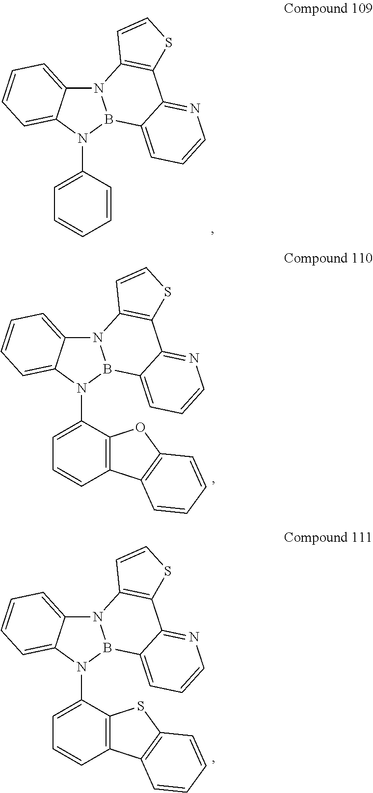
C00016

C00017
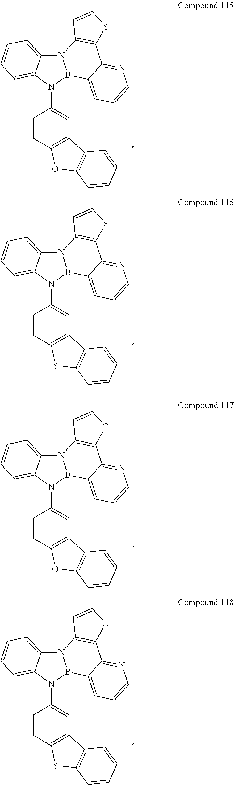
C00018
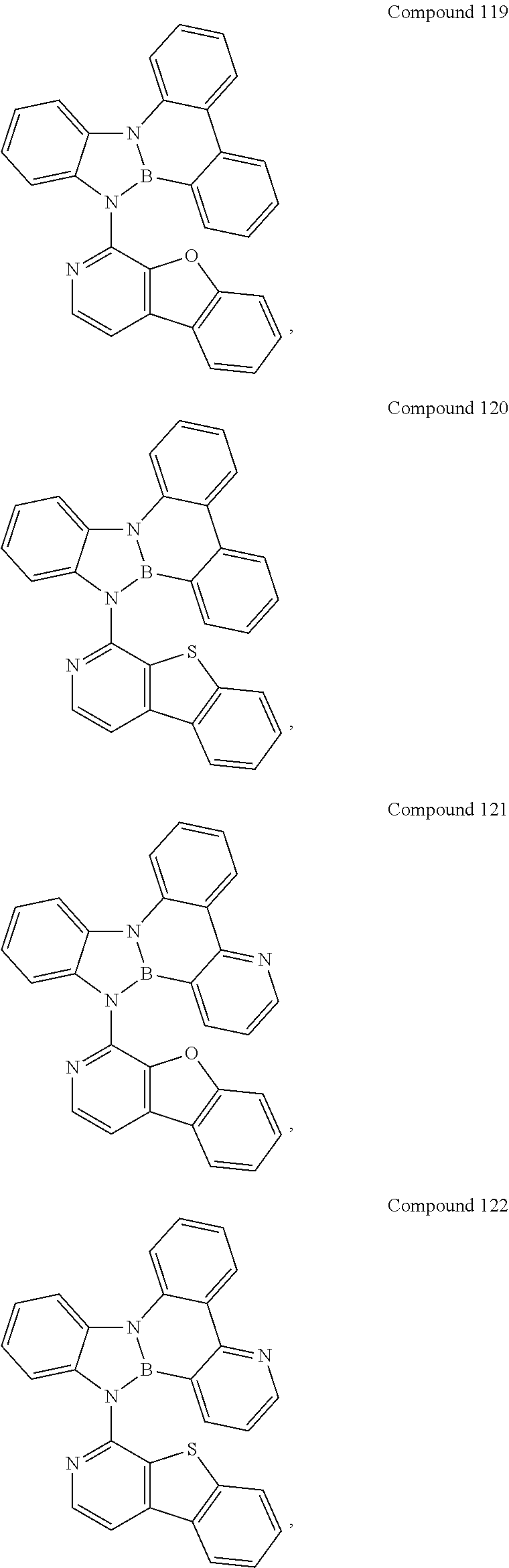
C00019

C00020

C00021

C00022

C00023
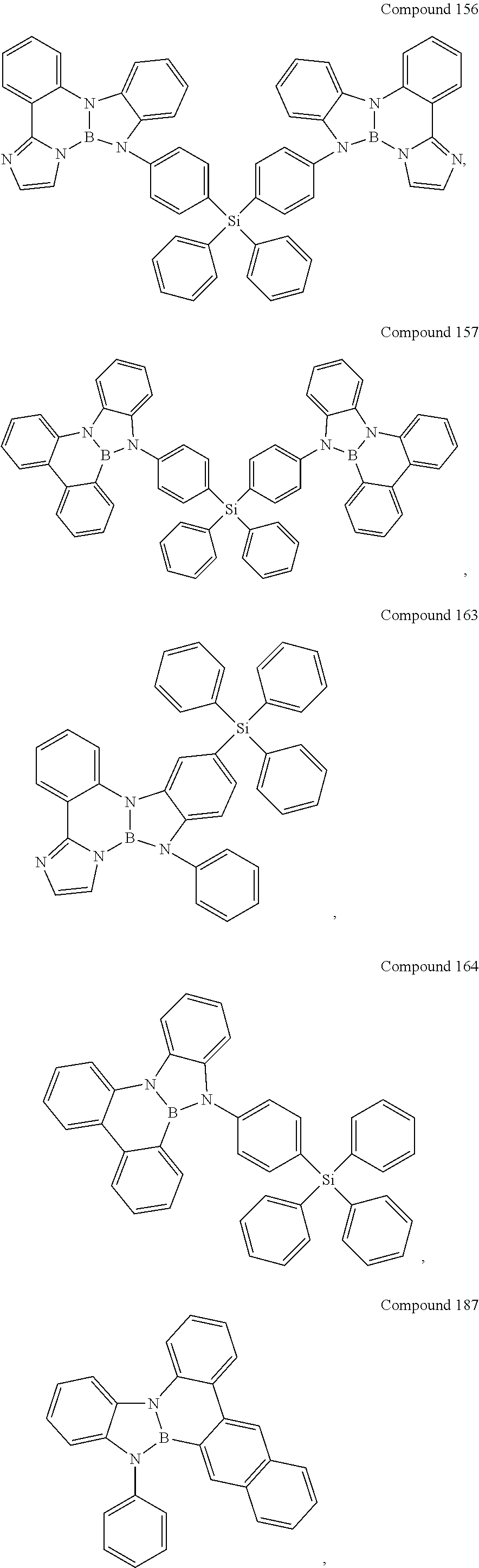
C00024
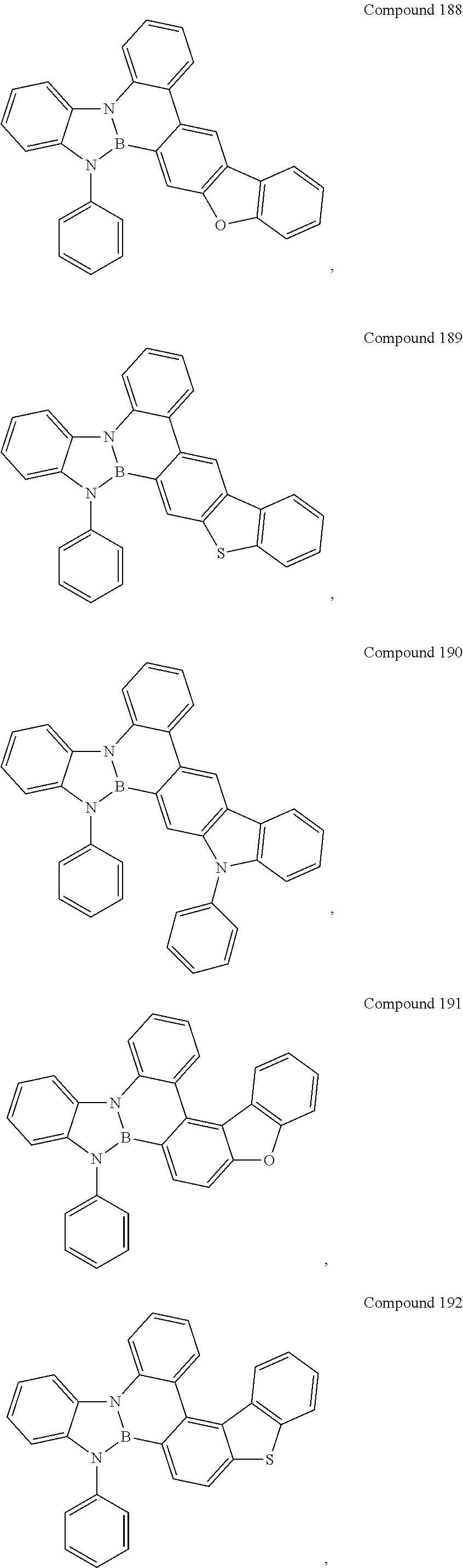
C00025

C00026
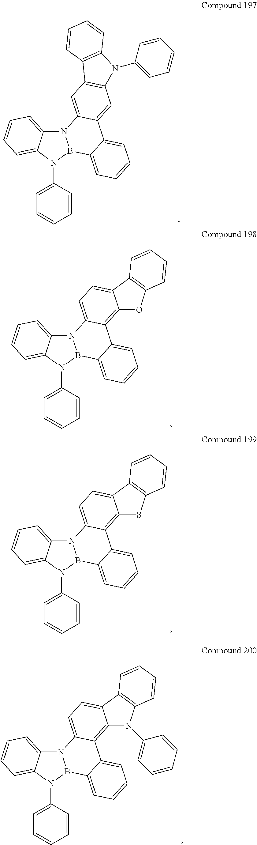
C00027
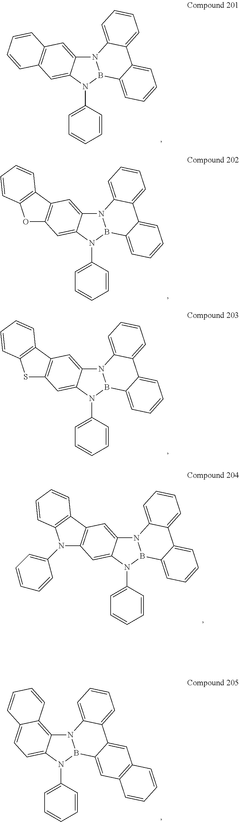
C00028
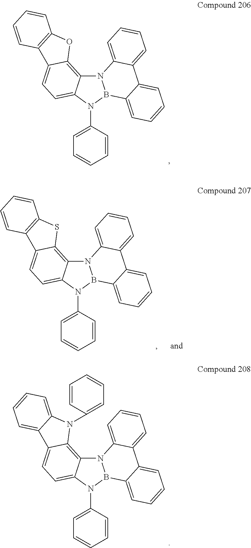
C00029

C00030
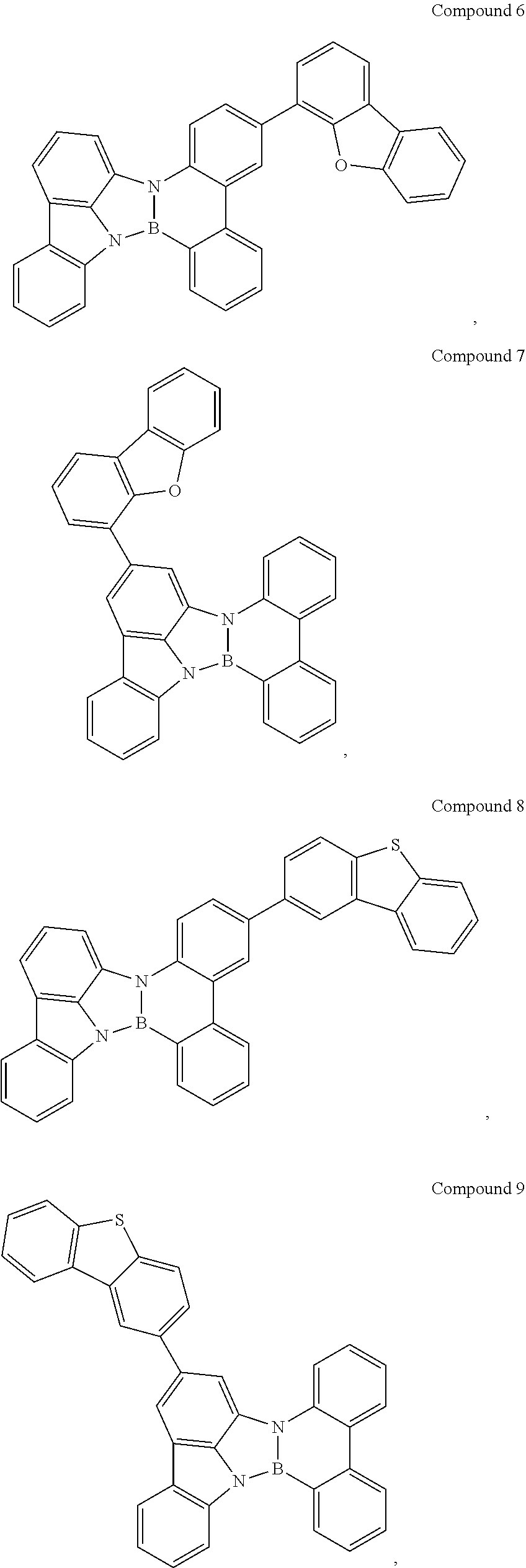
C00031

C00032
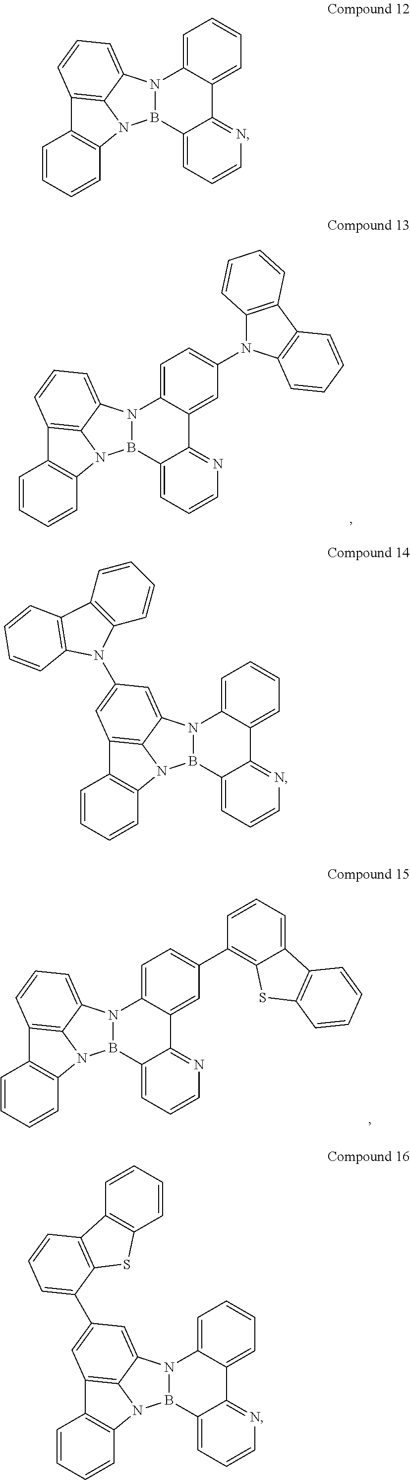
C00033

C00034

C00035
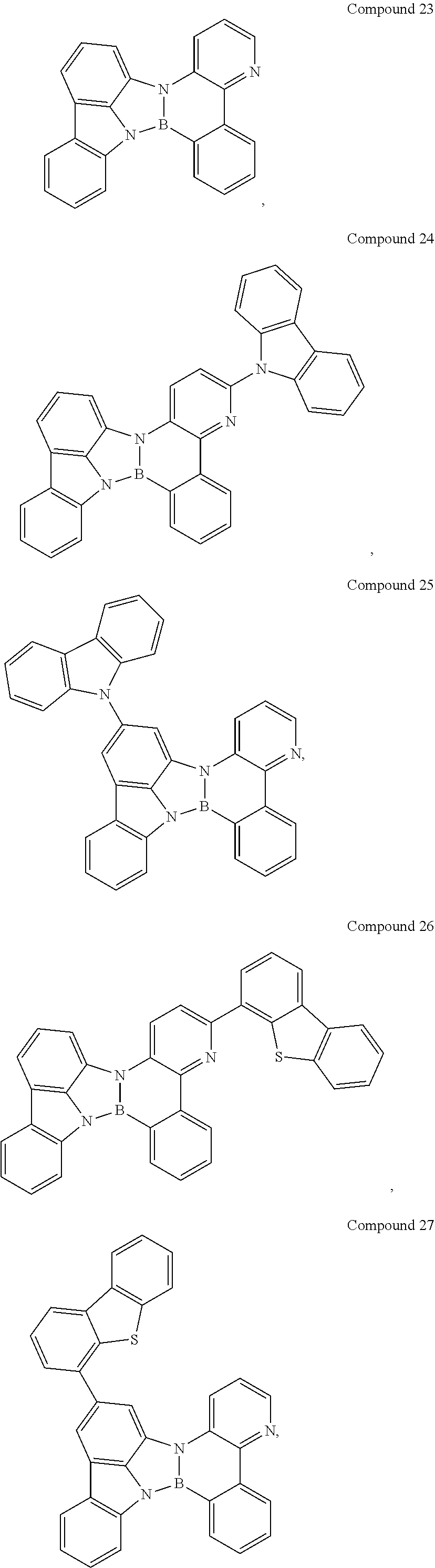
C00036
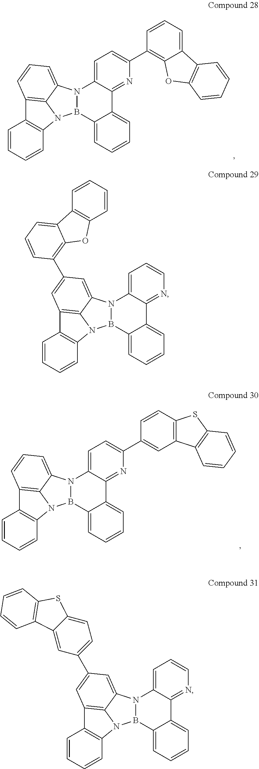
C00037
C00038
C00039

C00040

C00041
C00042
C00043
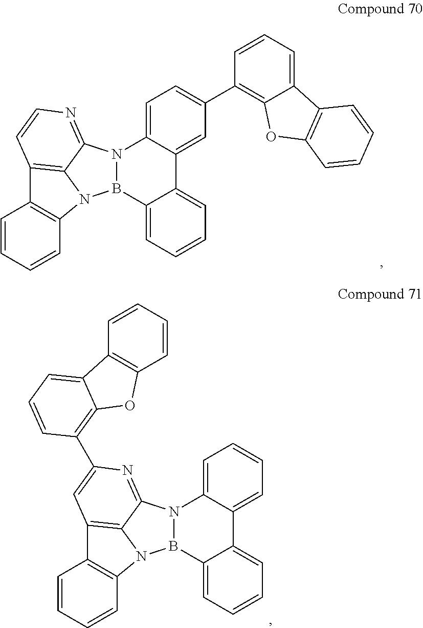
C00044

C00045

C00046
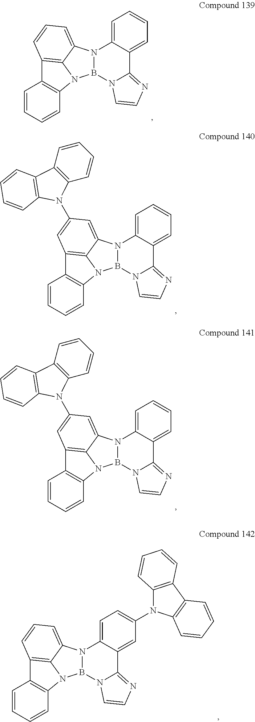
C00047

C00048
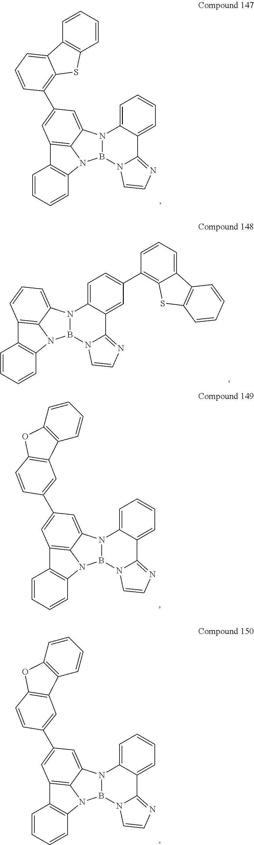
C00049
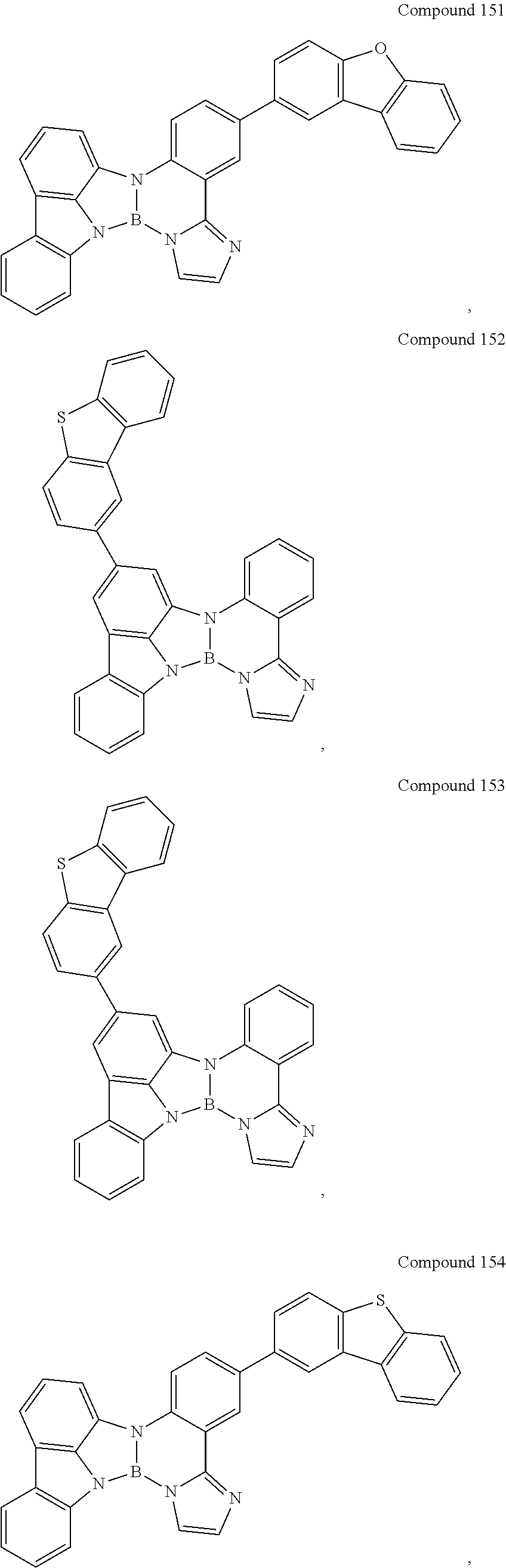
C00050
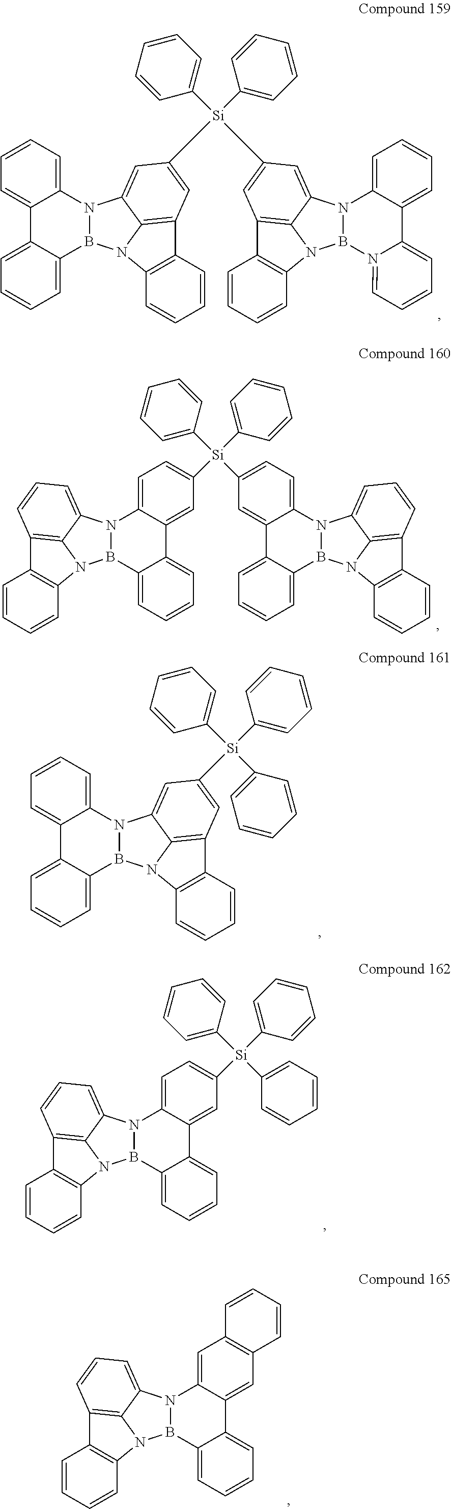
C00051
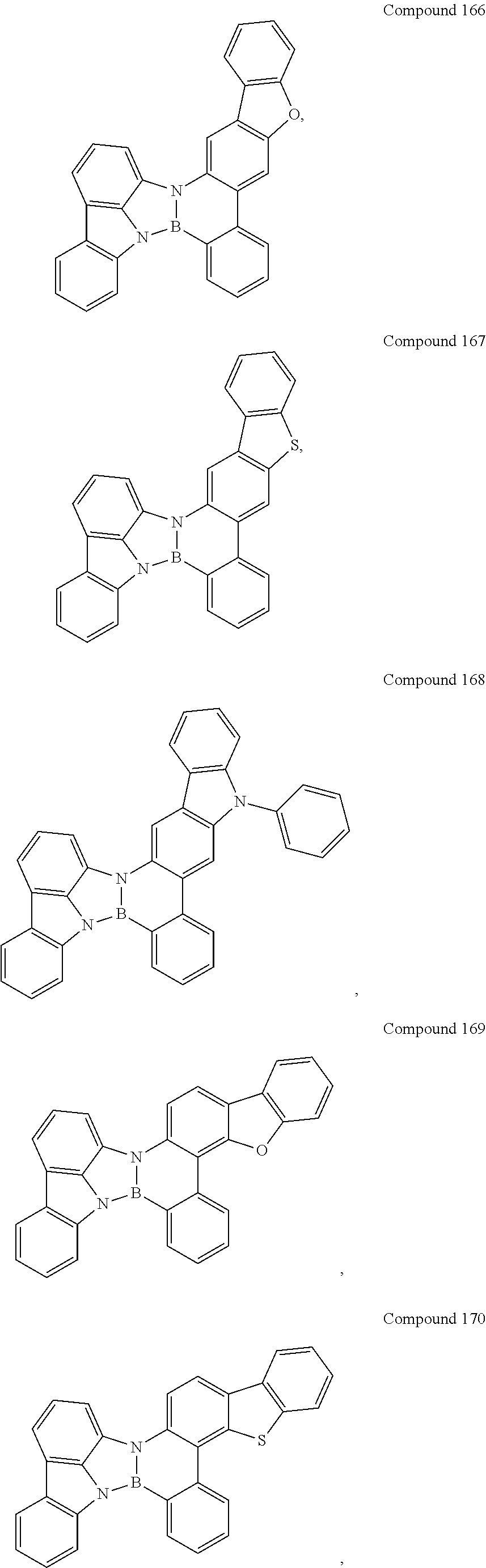
C00052

C00053
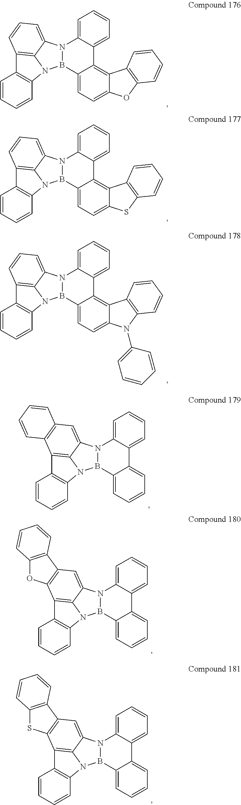
C00054
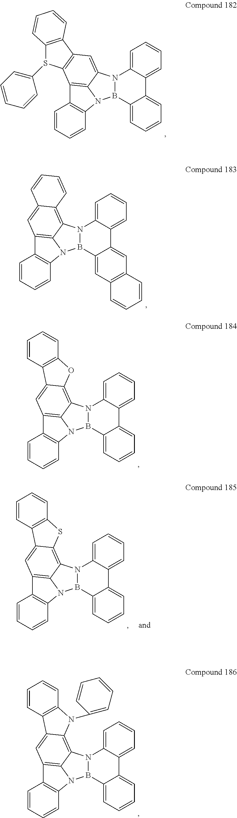
C00055
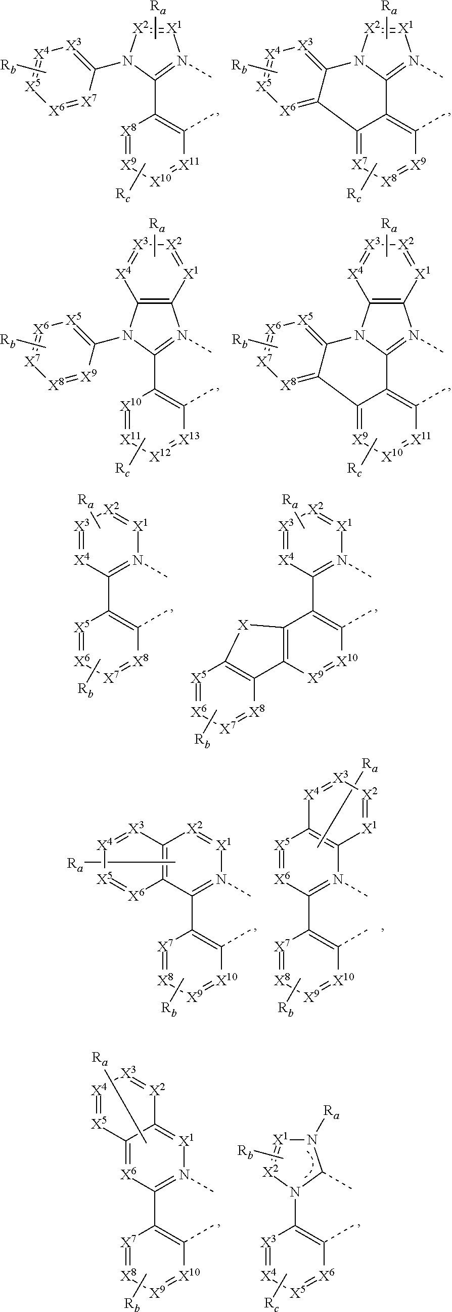
C00056
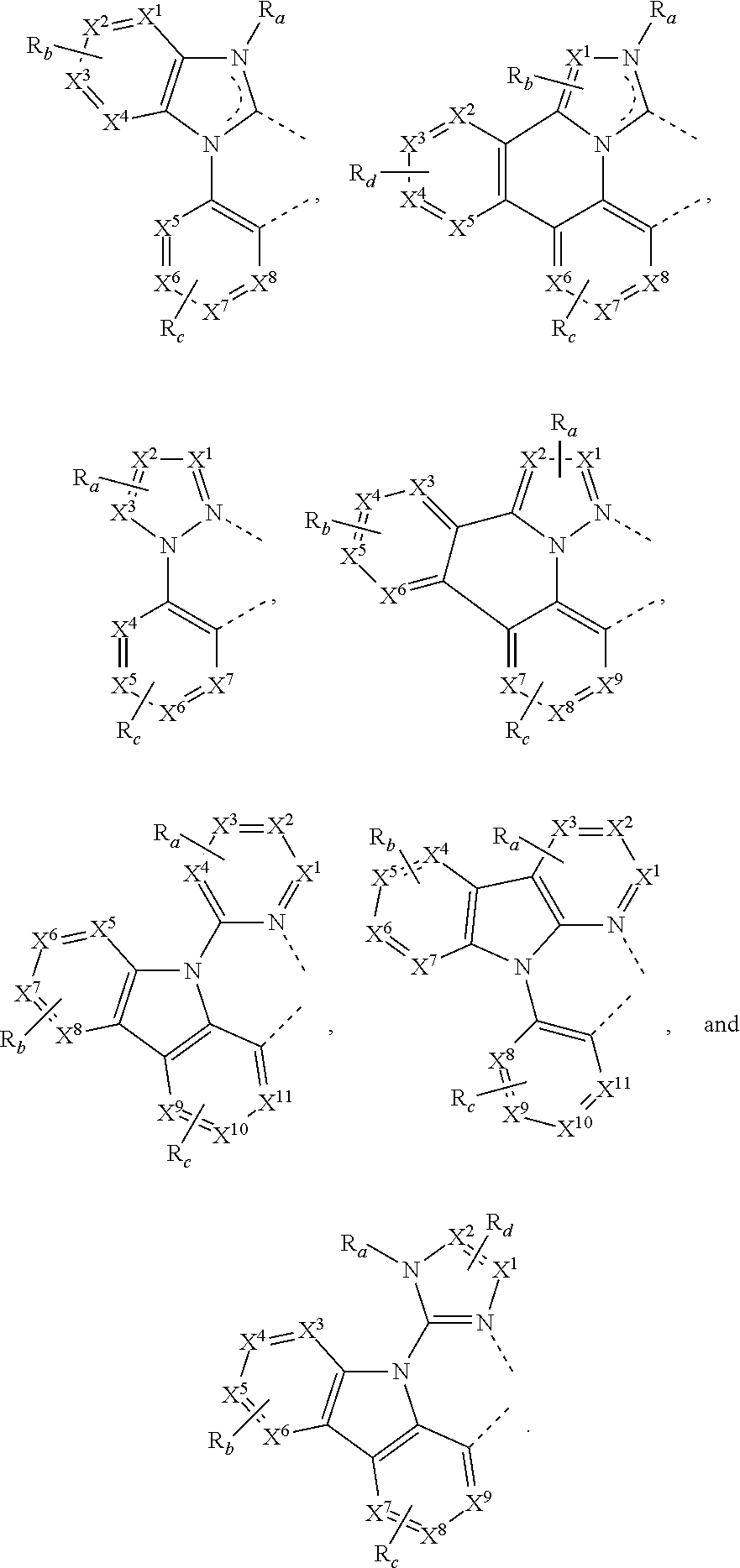
C00057
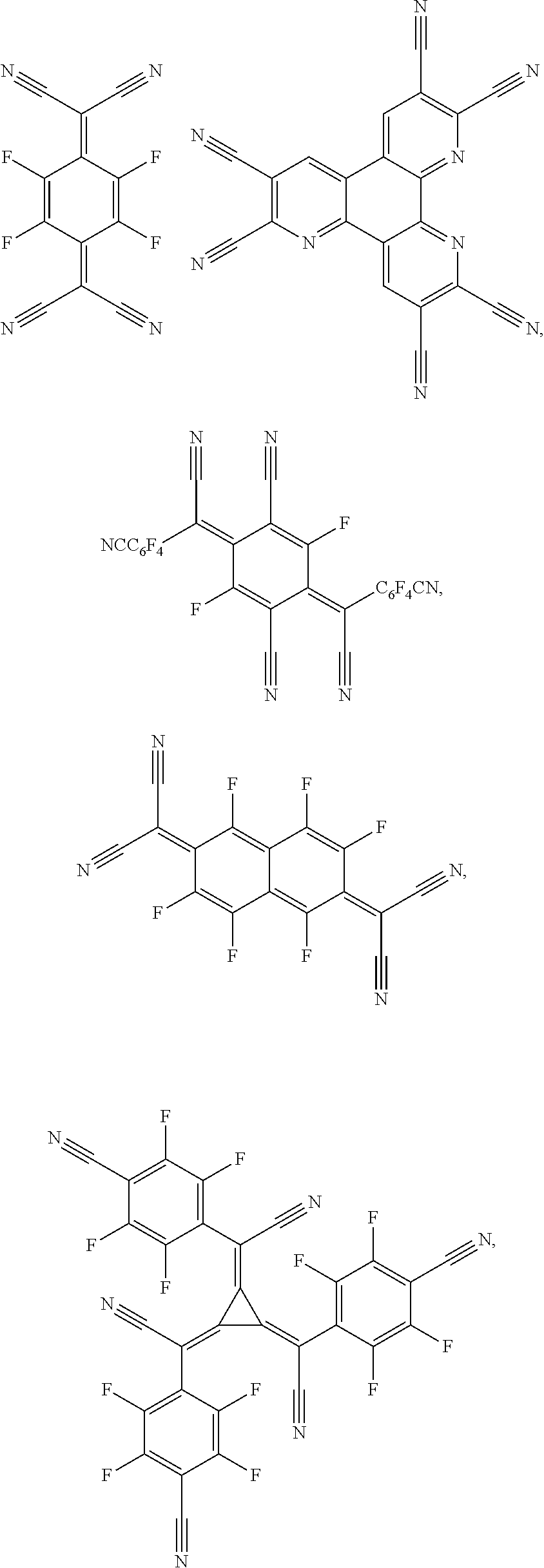
C00058
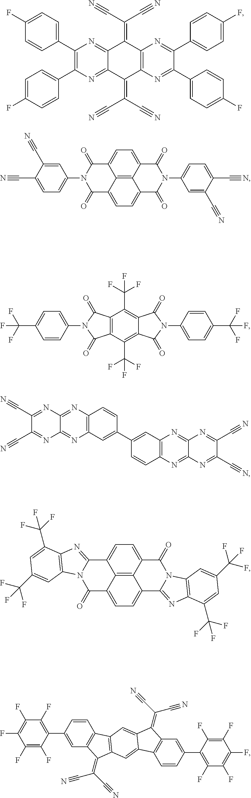
C00059
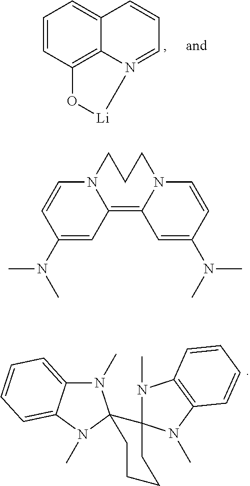
C00060
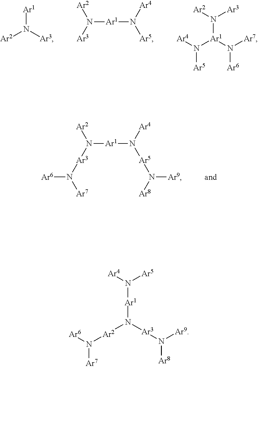
C00061
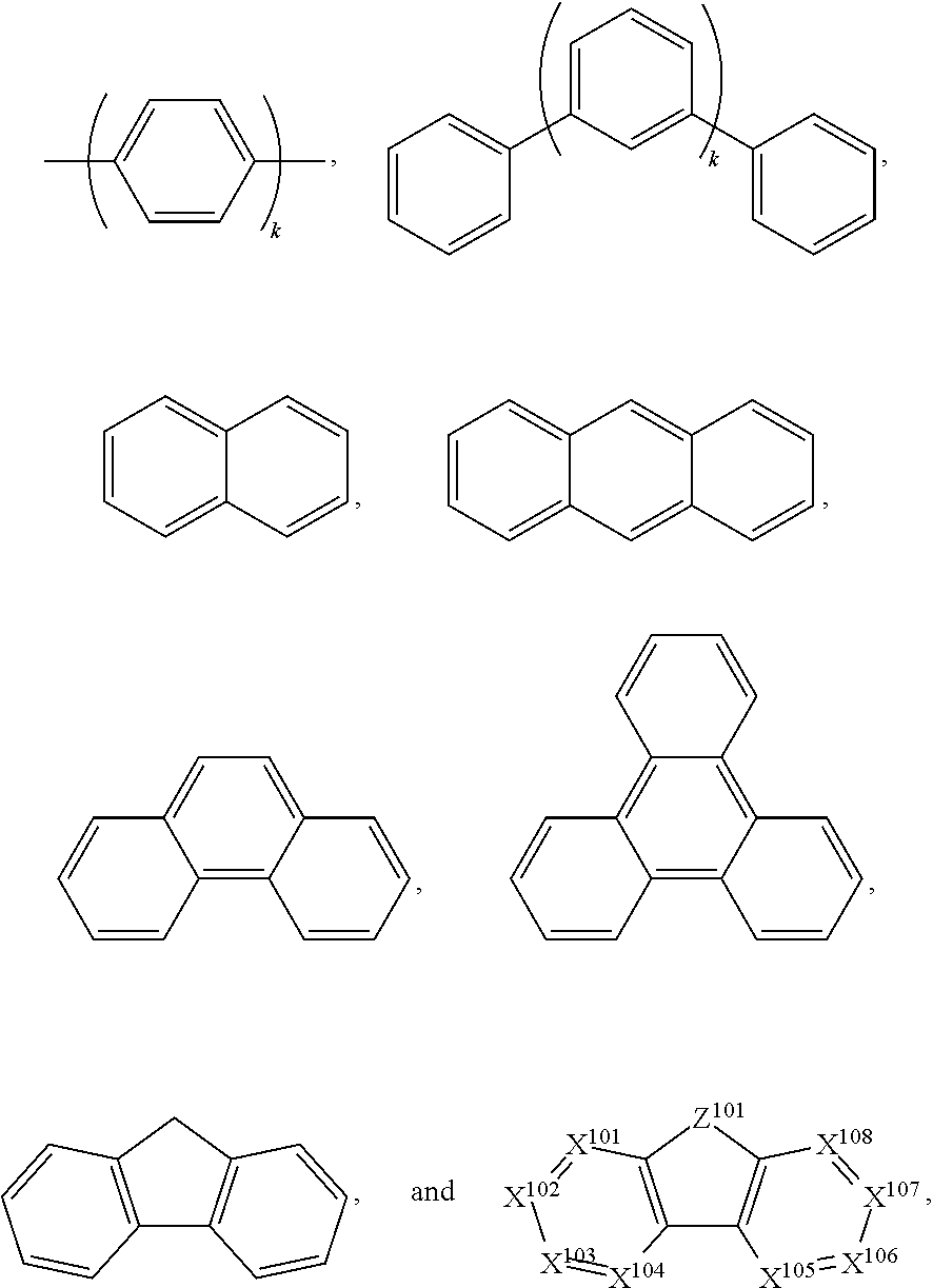
C00062
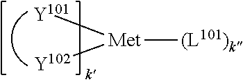
C00063
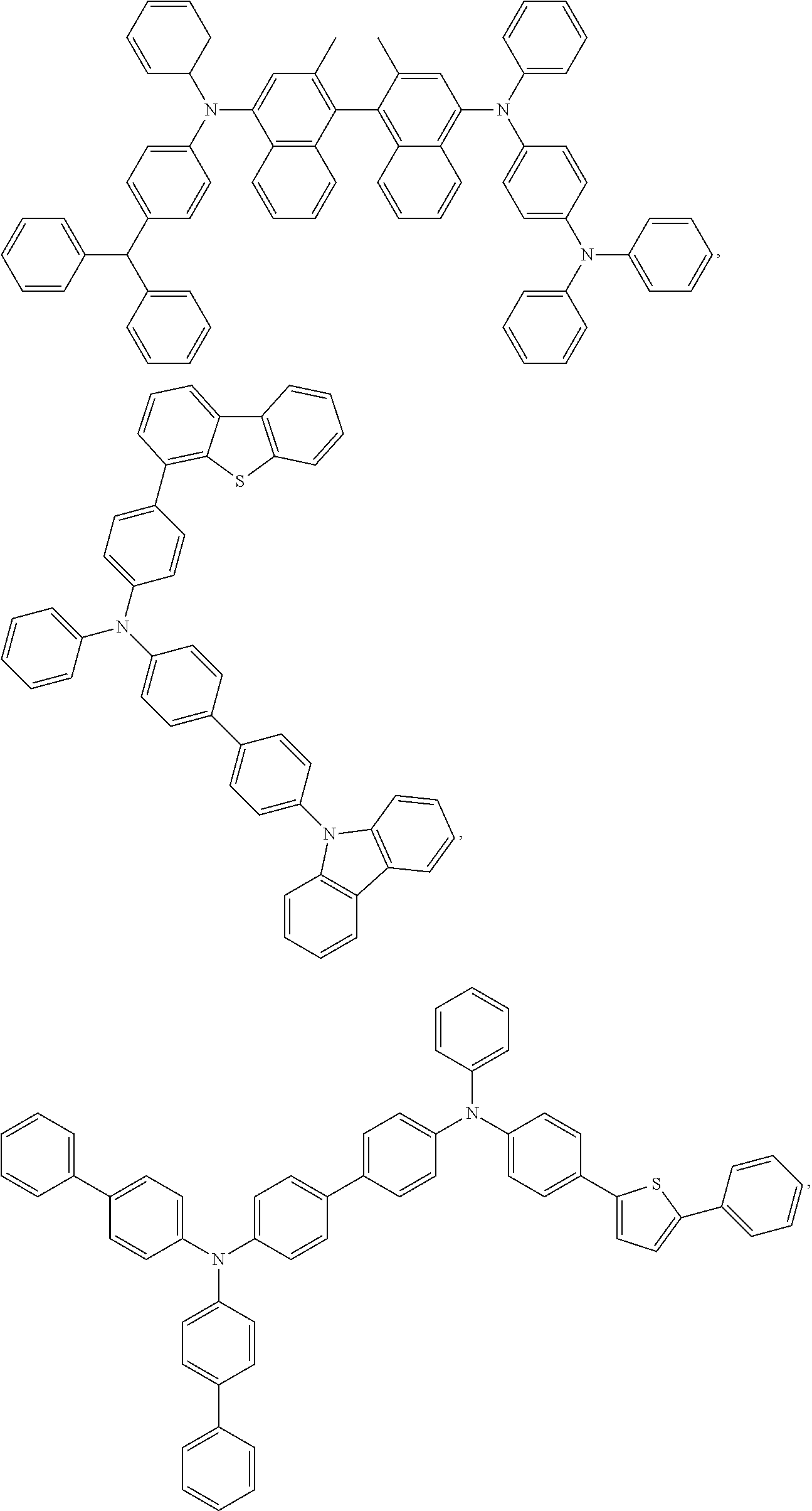
C00064
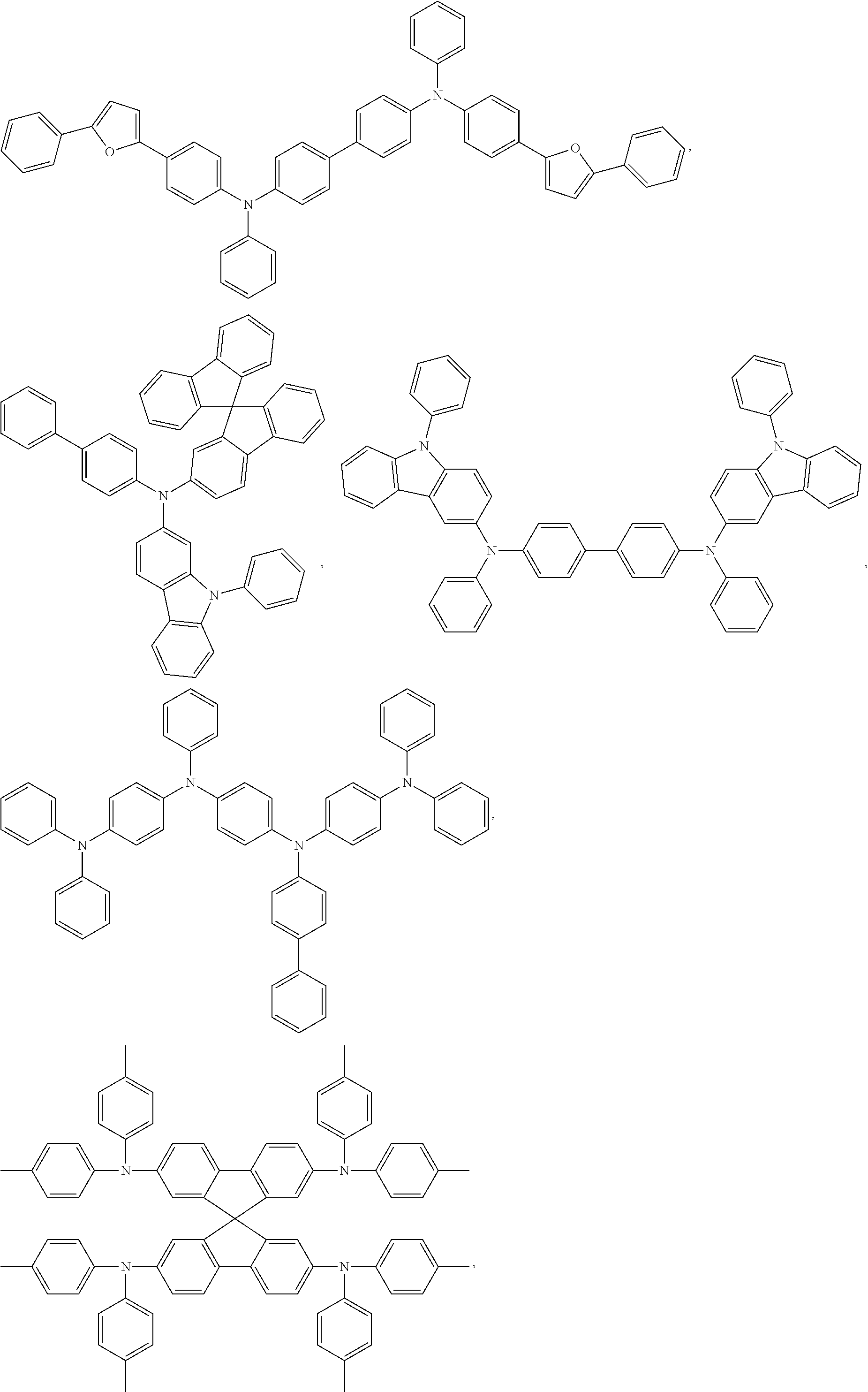
C00065
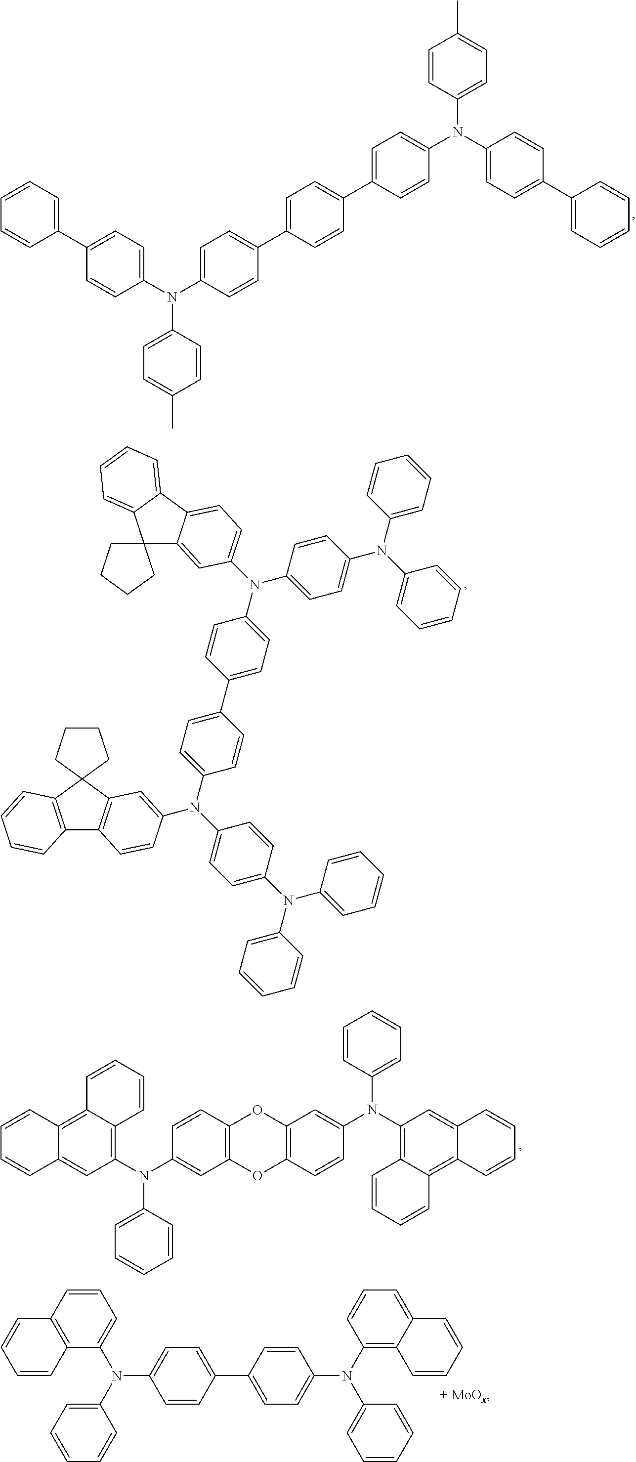
C00066
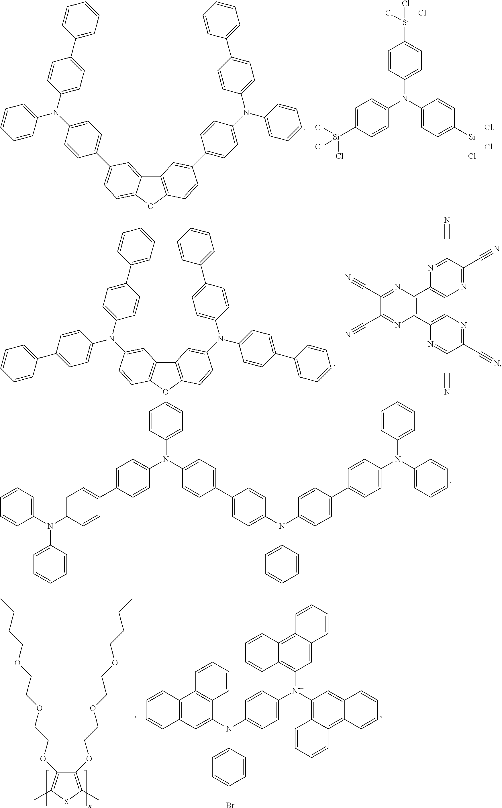
C00067

C00068
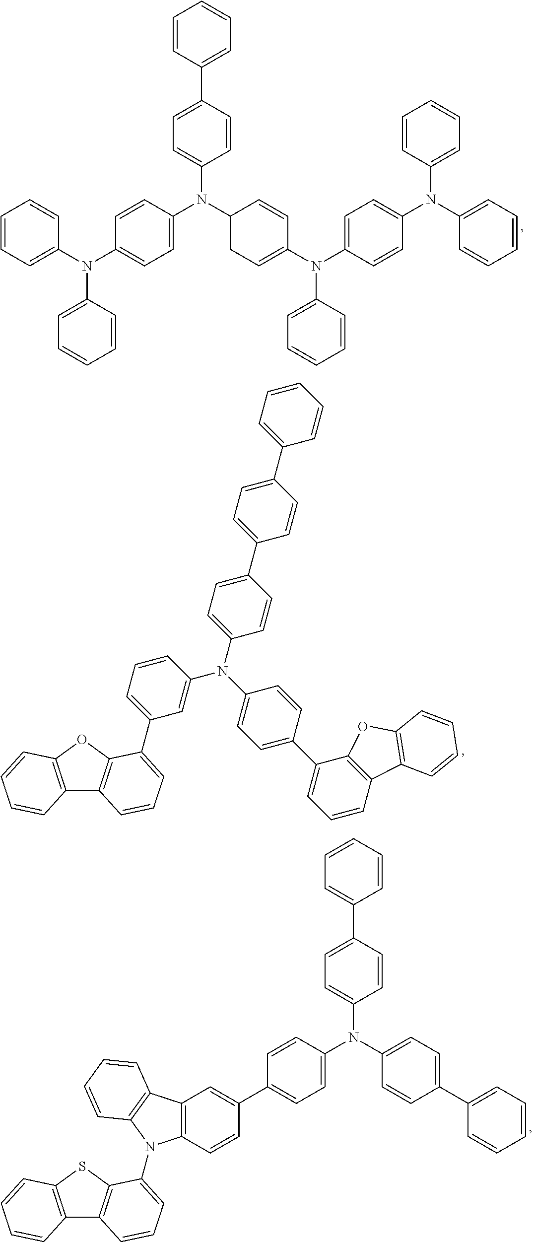
C00069
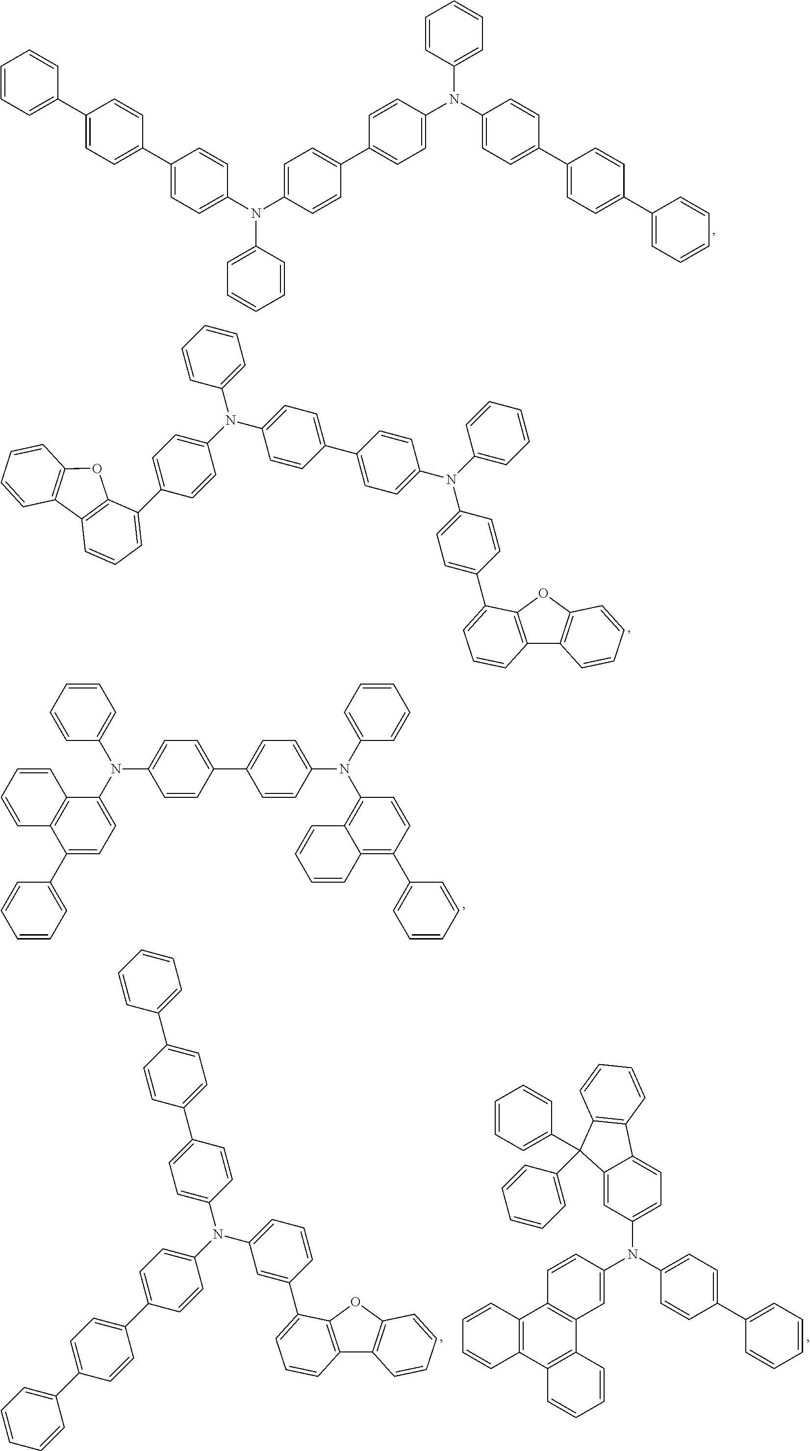
C00070
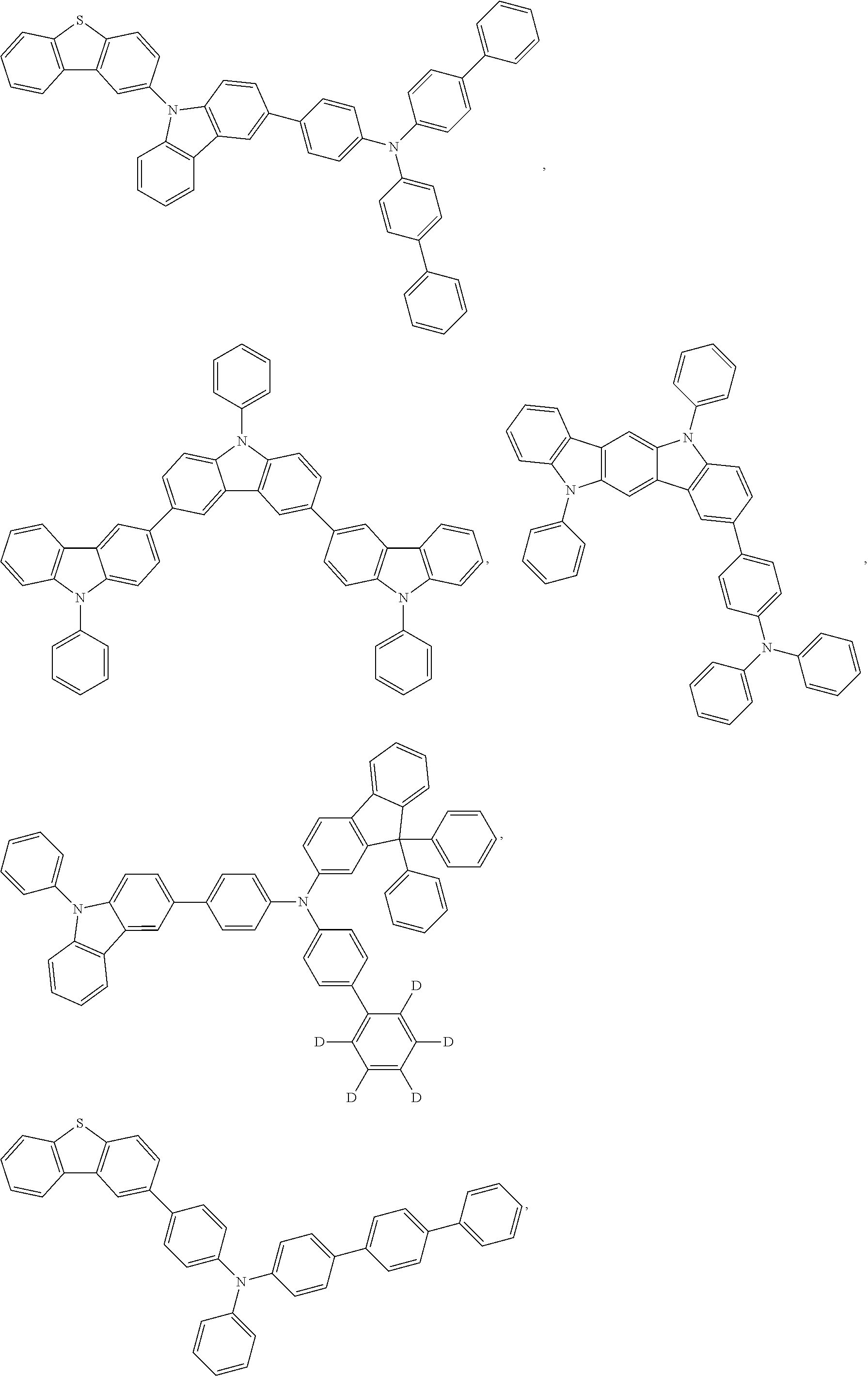
C00071
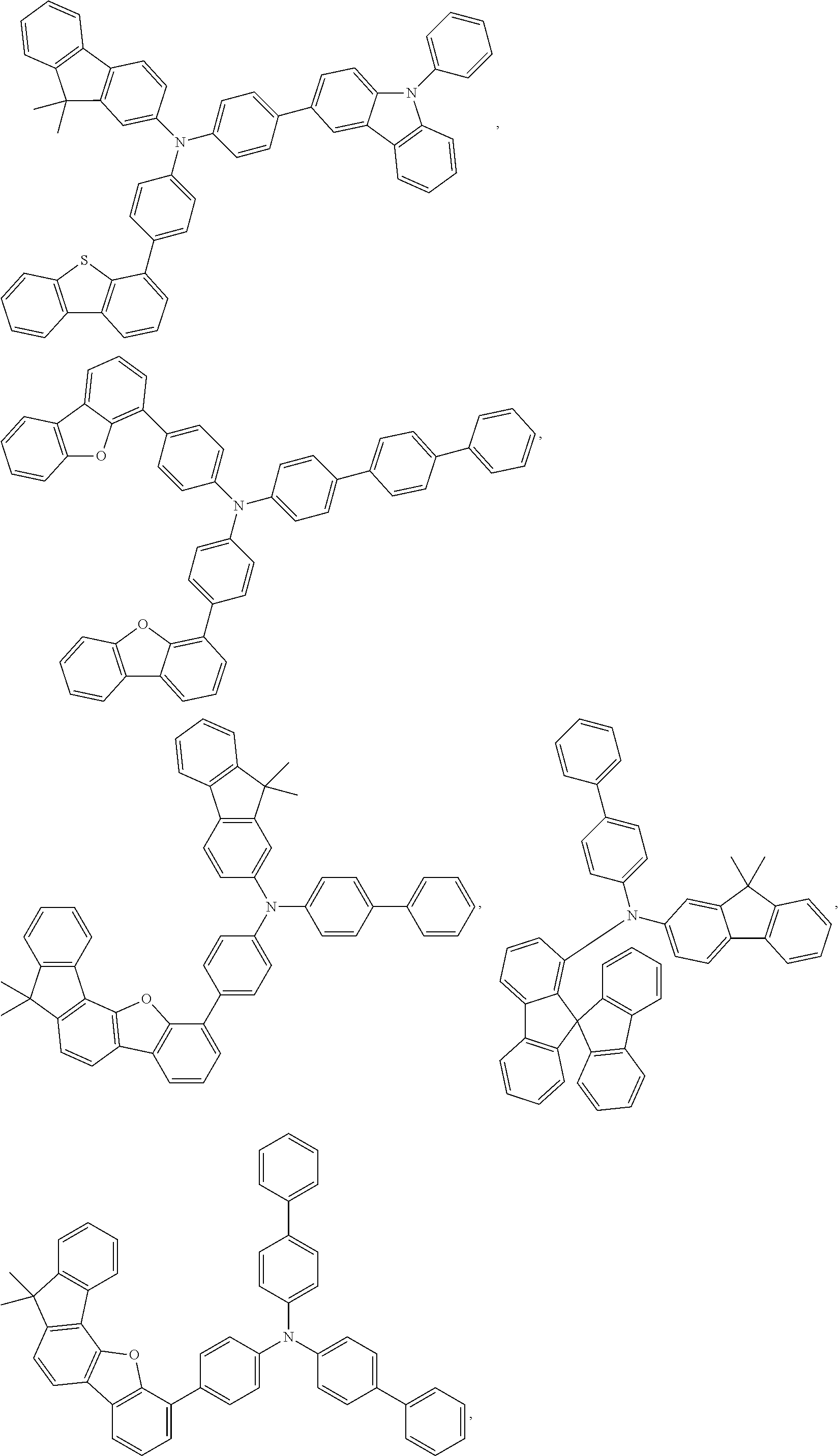
C00072
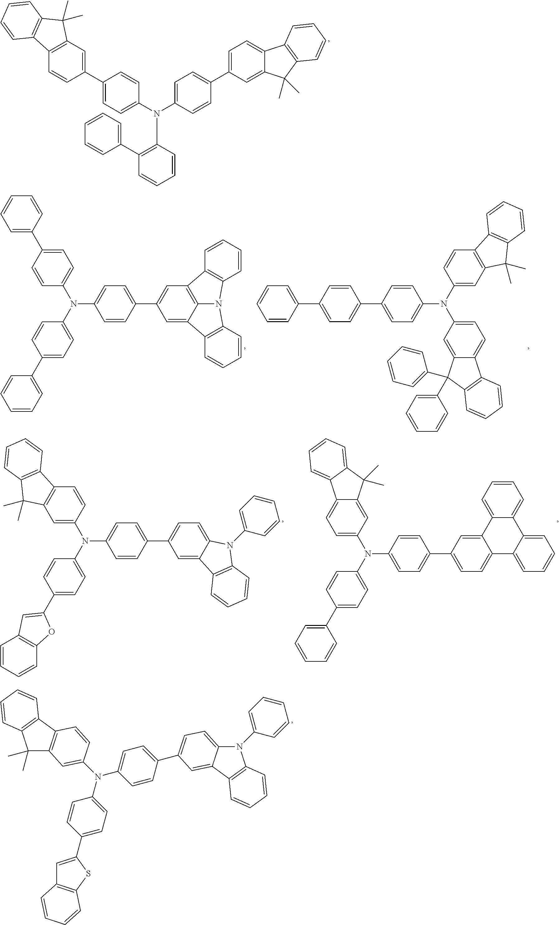
C00073
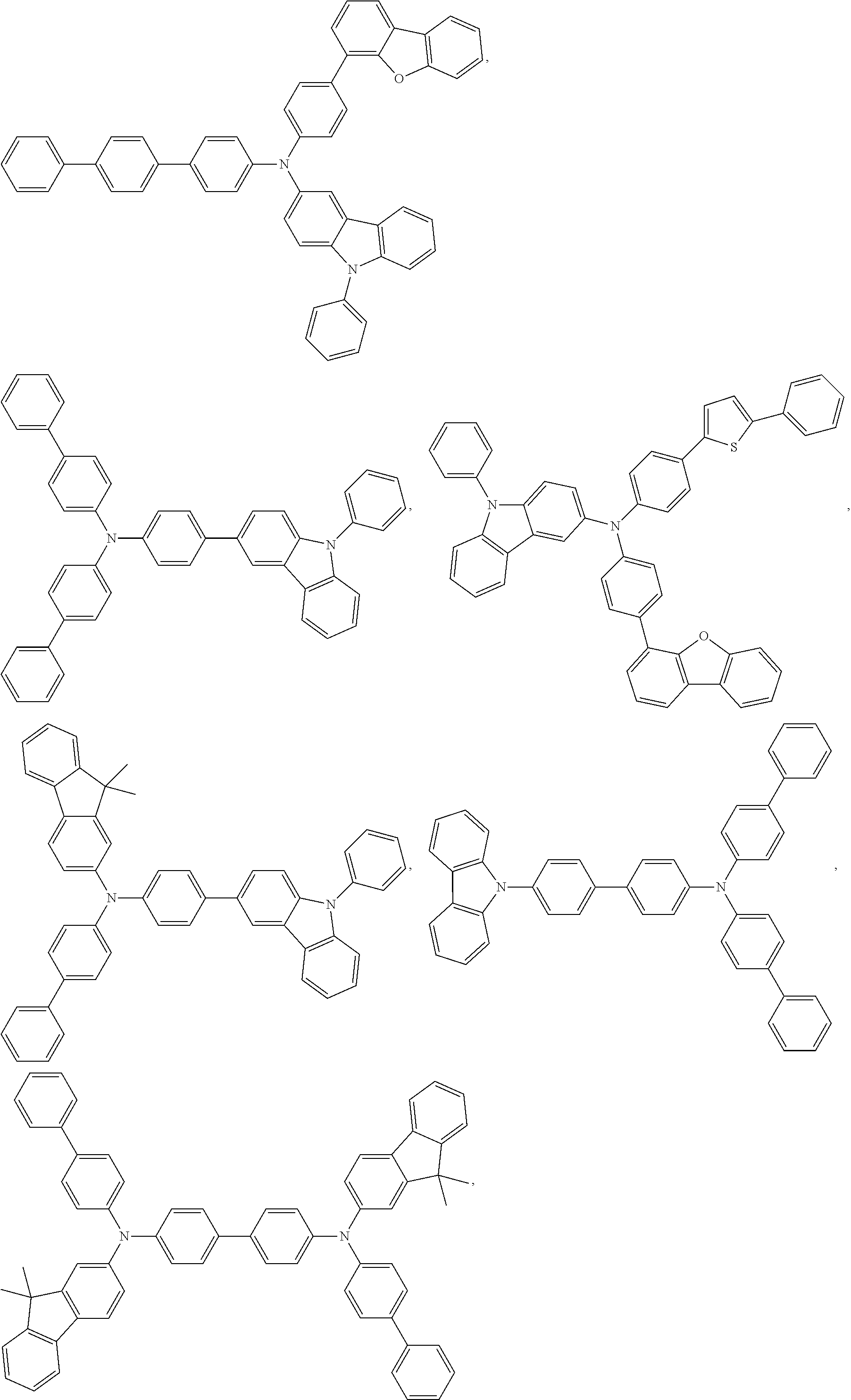
C00074
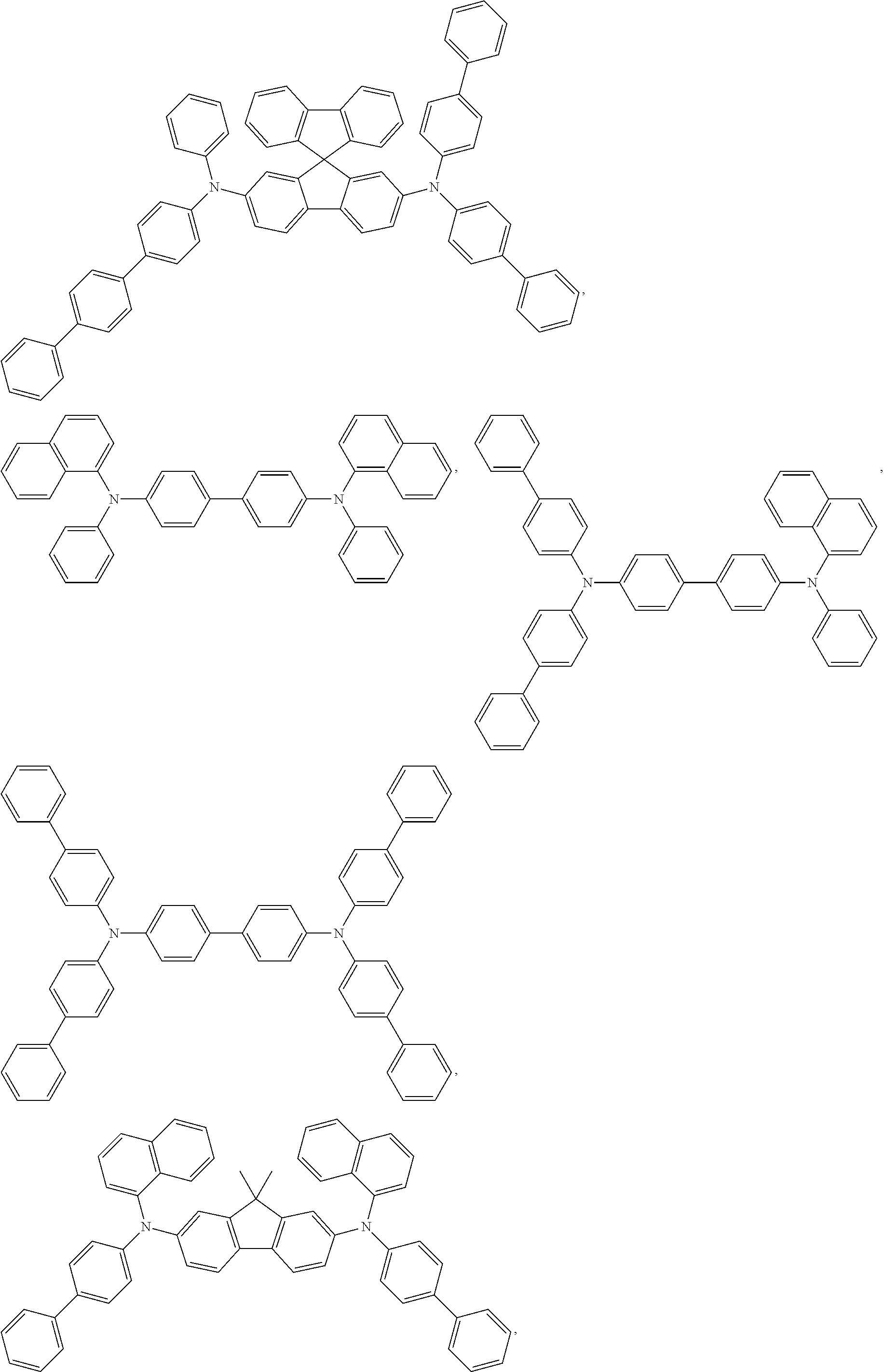
C00075

C00076
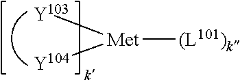
C00077
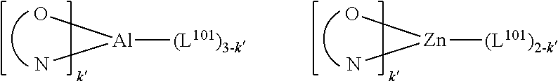
C00078
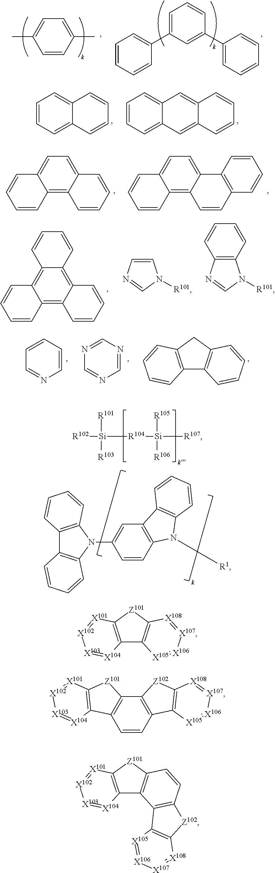
C00079
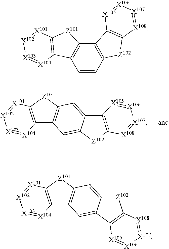
C00080

C00081

C00082
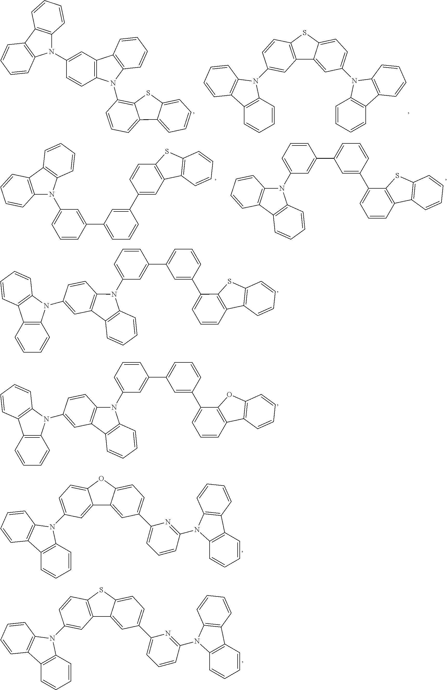
C00083

C00084
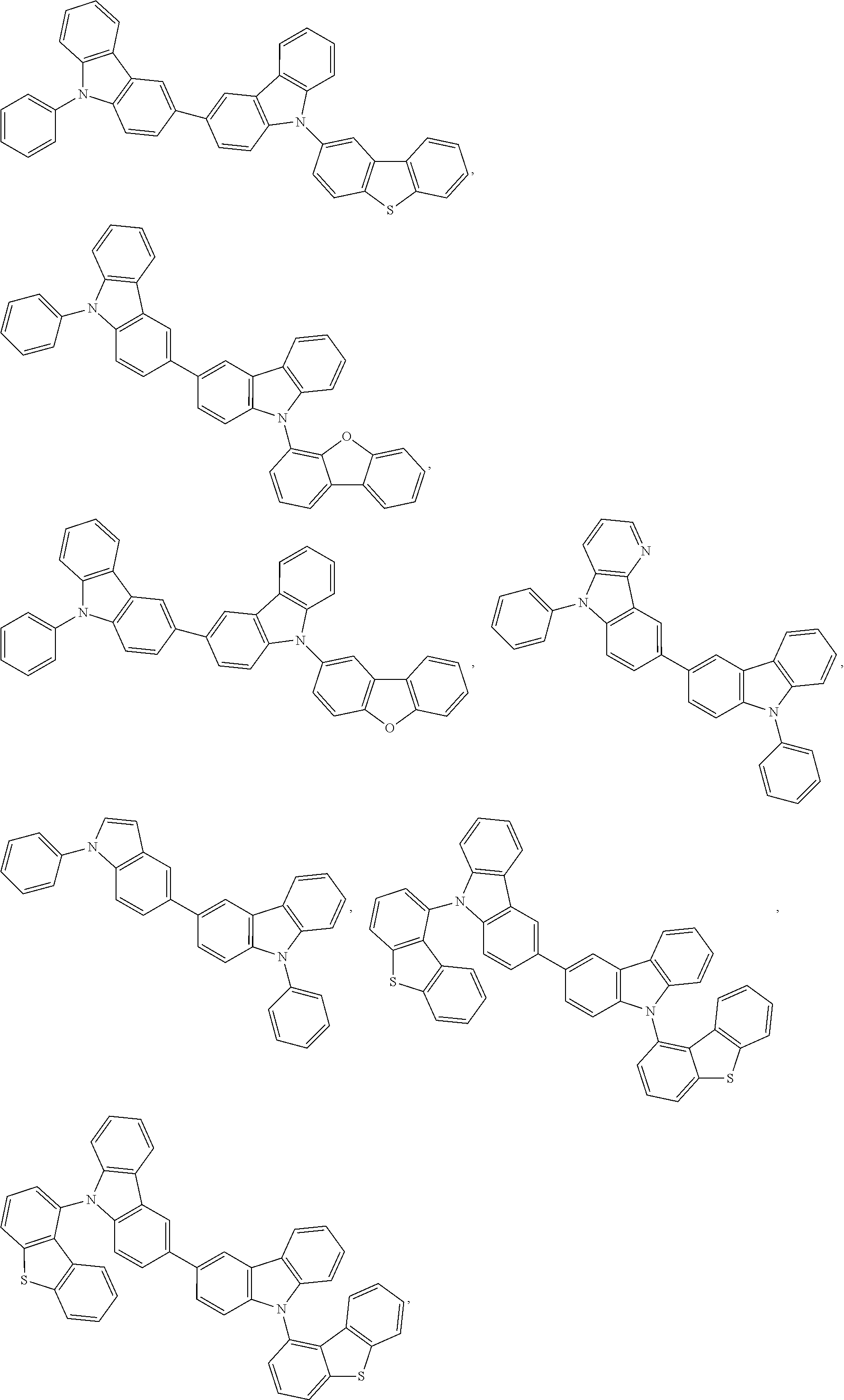
C00085
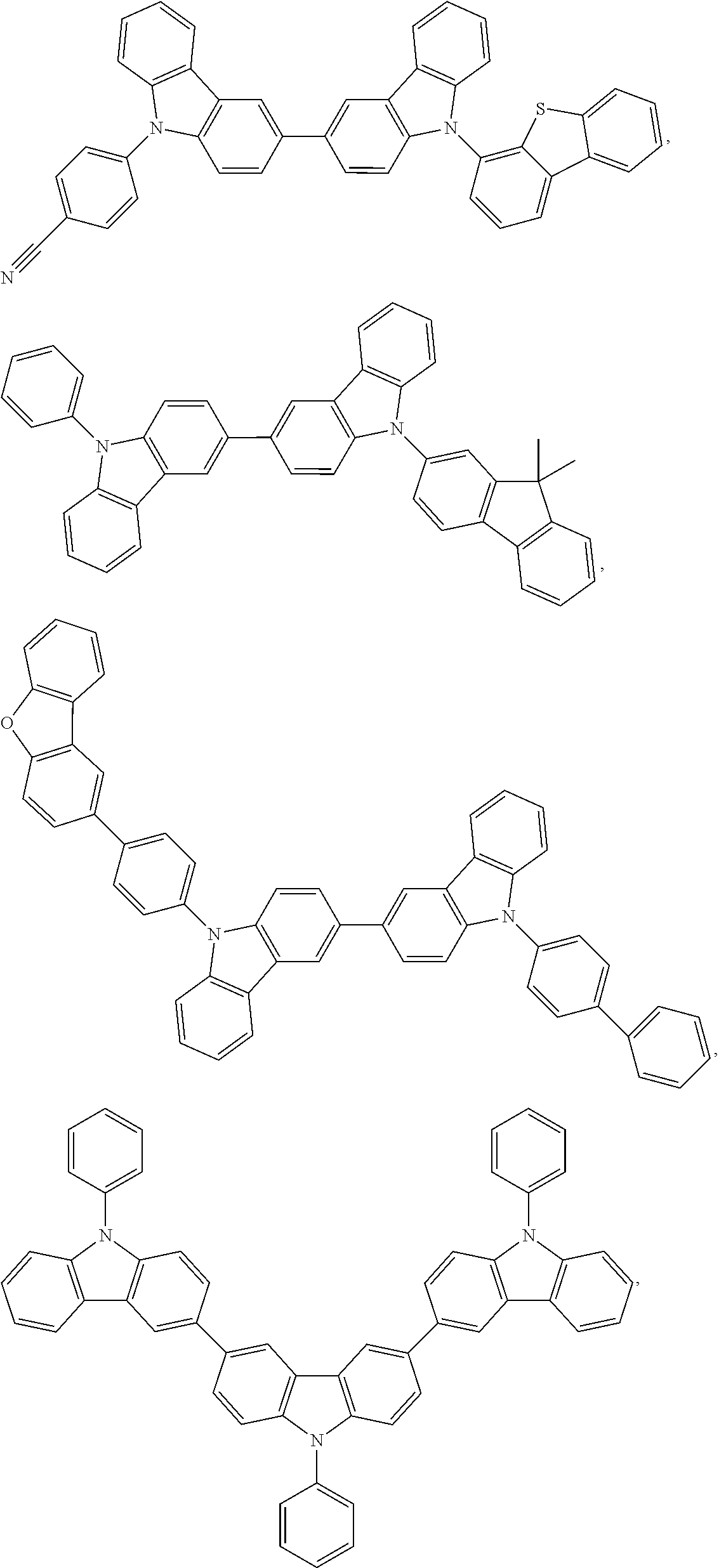
C00086
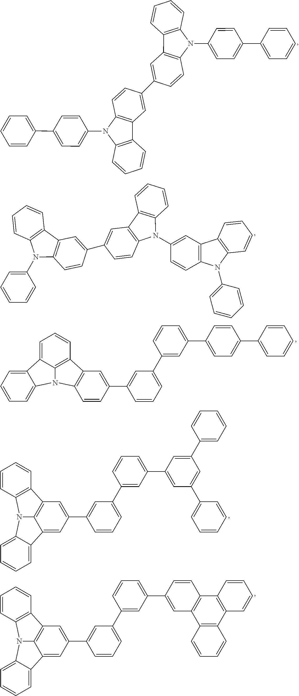
C00087

C00088
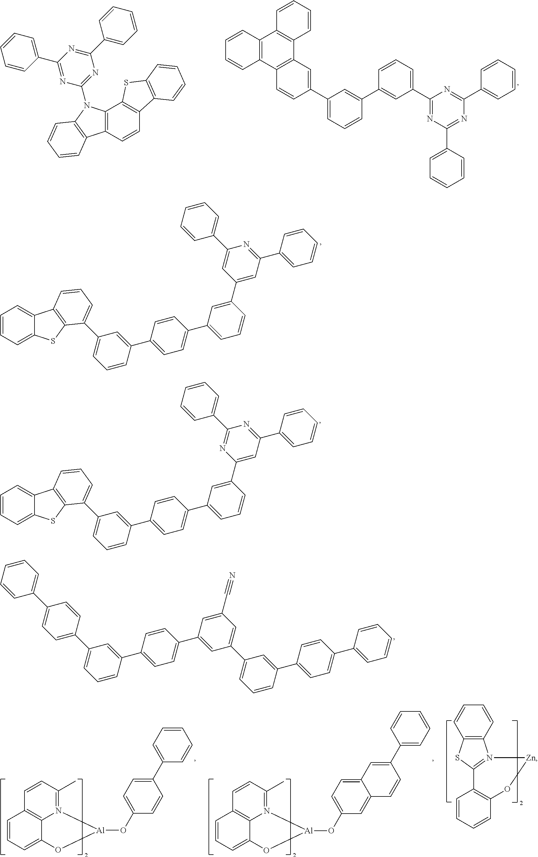
C00089

C00090

C00091
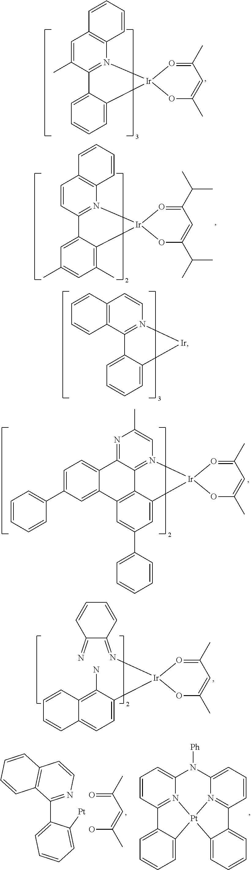
C00092

C00093

C00094
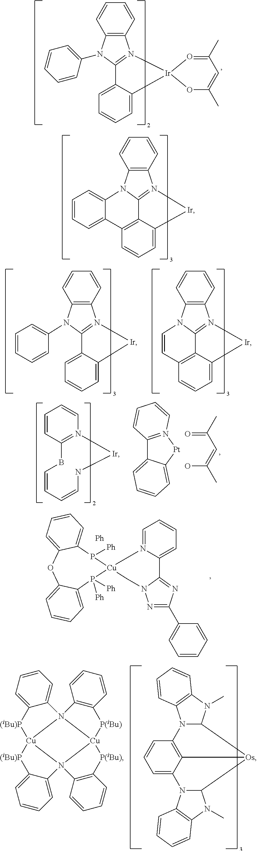
C00095
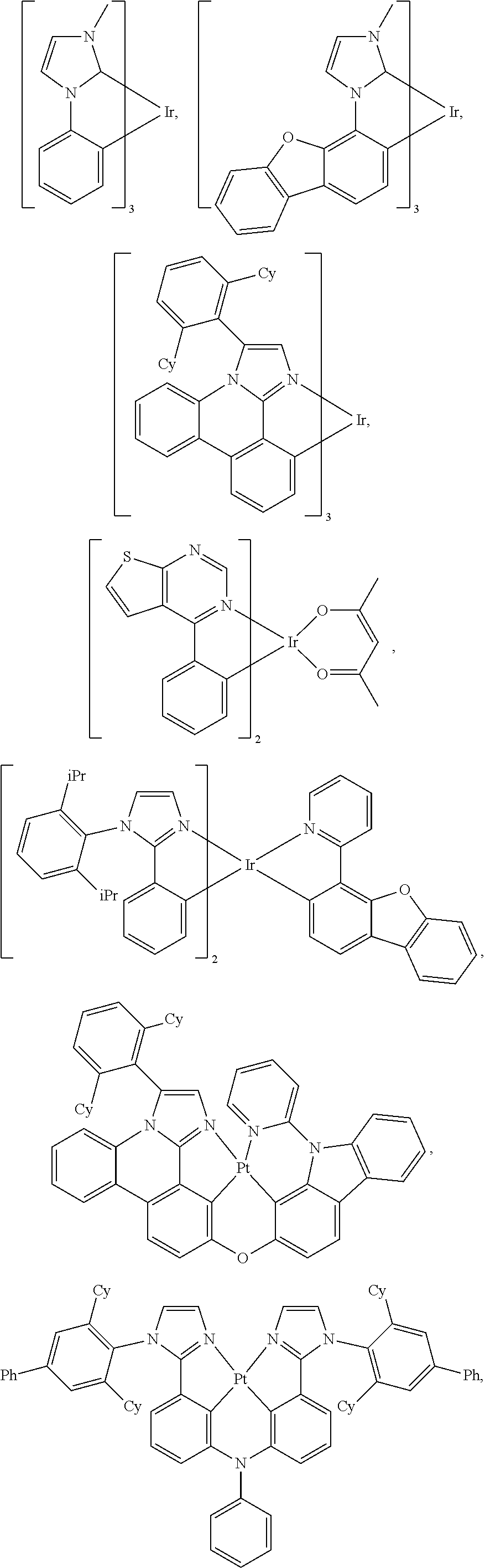
C00096
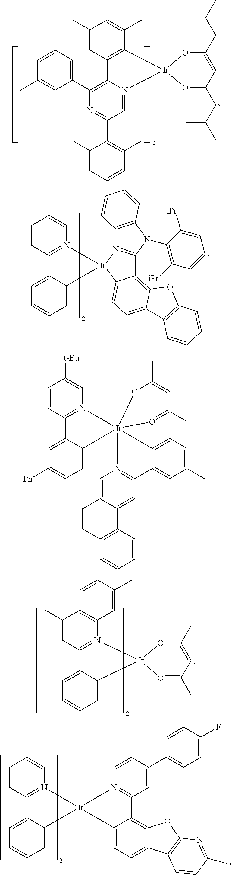
C00097
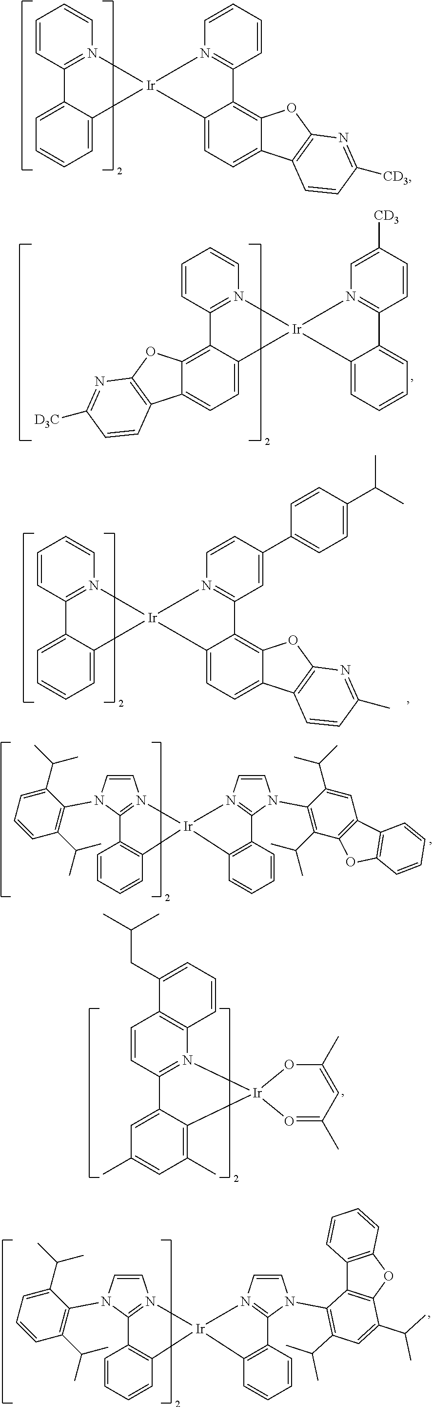
C00098
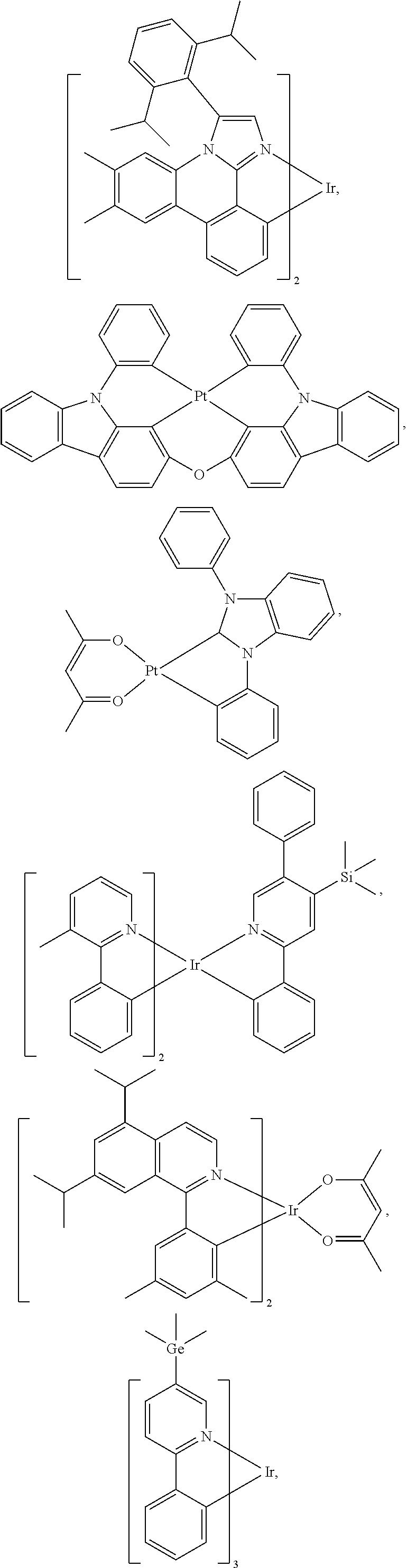
C00099
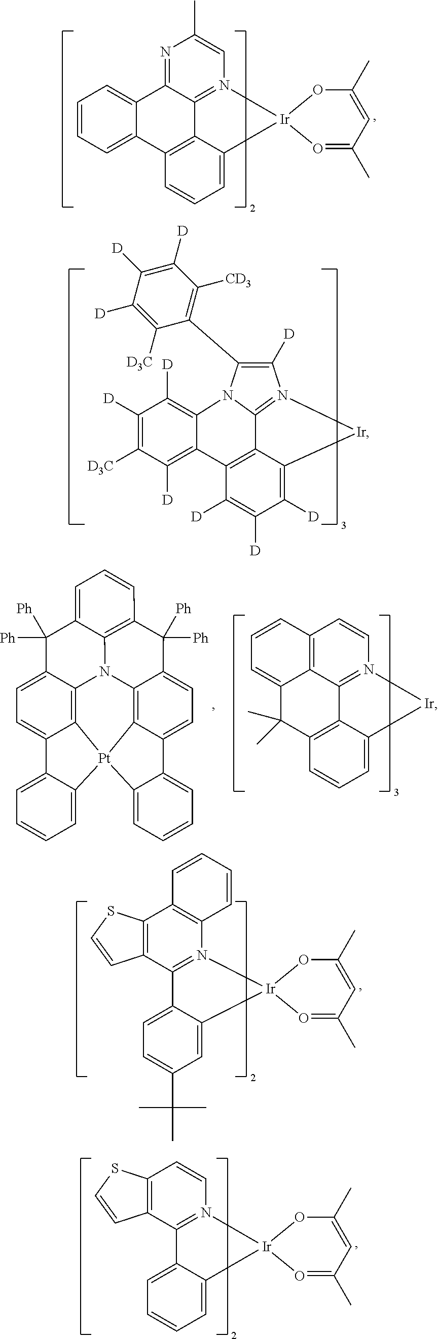
C00100
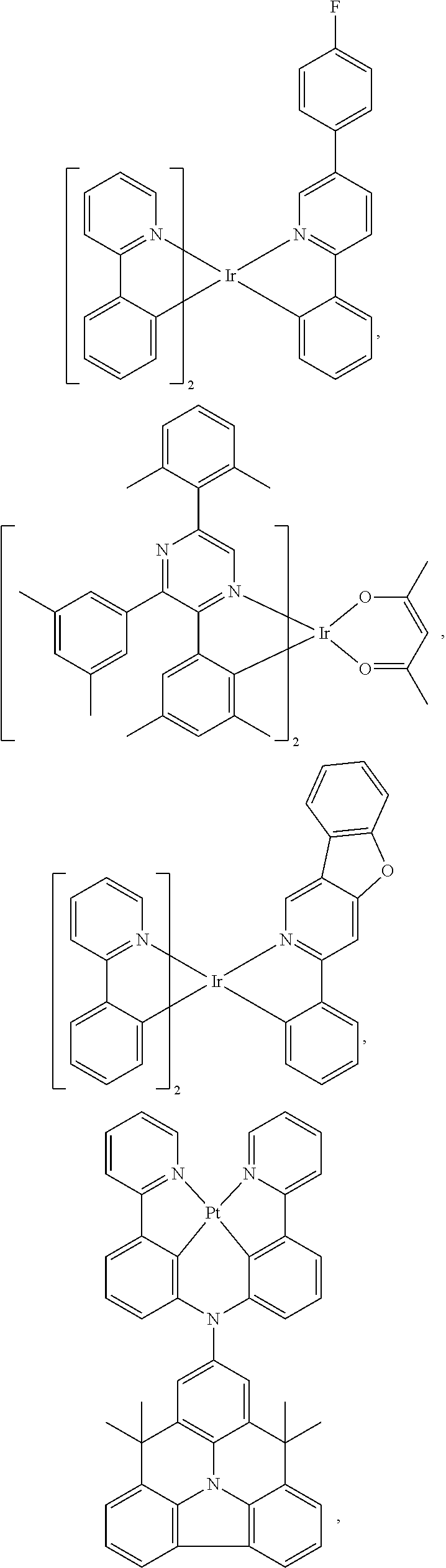
C00101
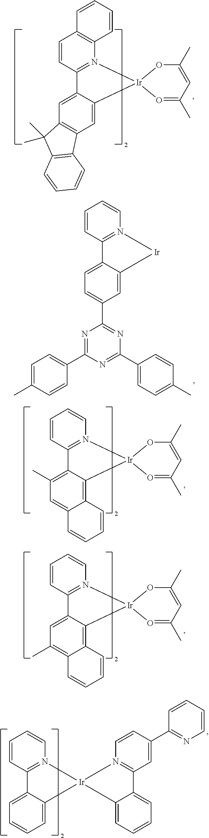
C00102
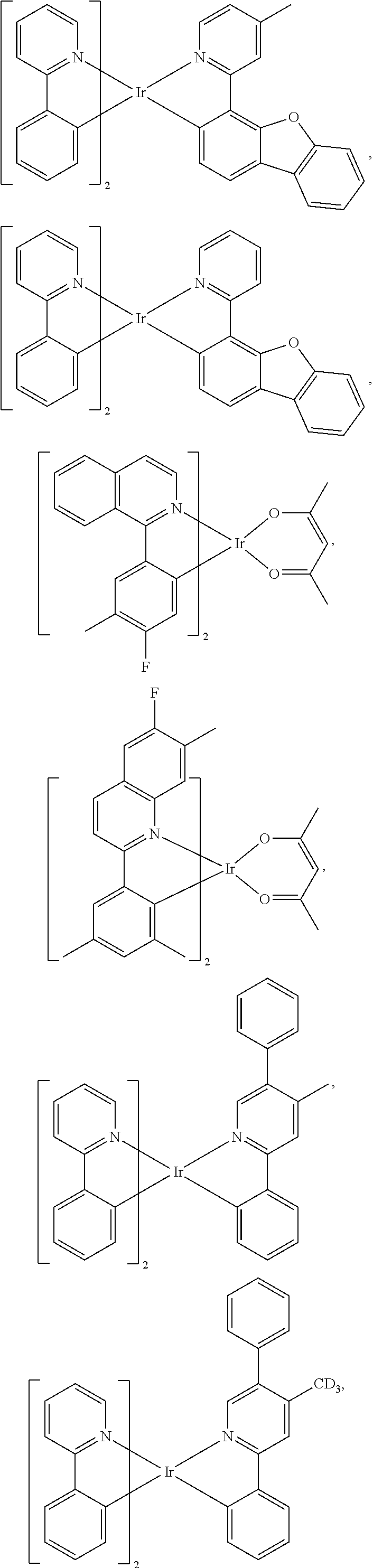
C00103
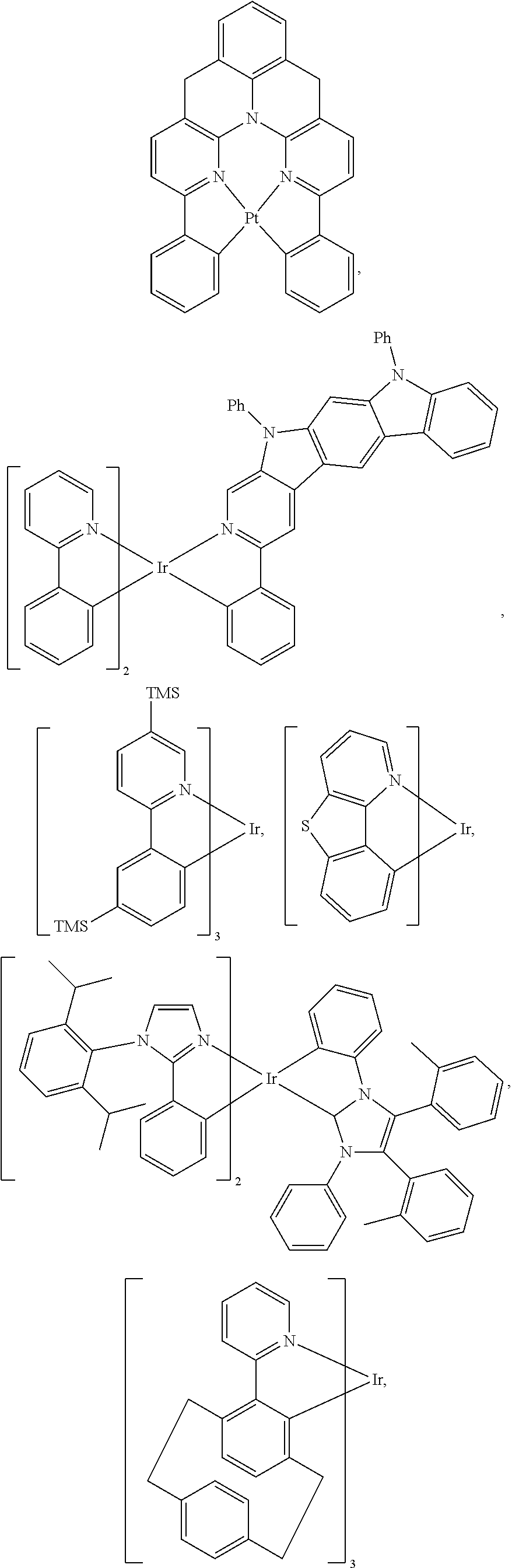
C00104
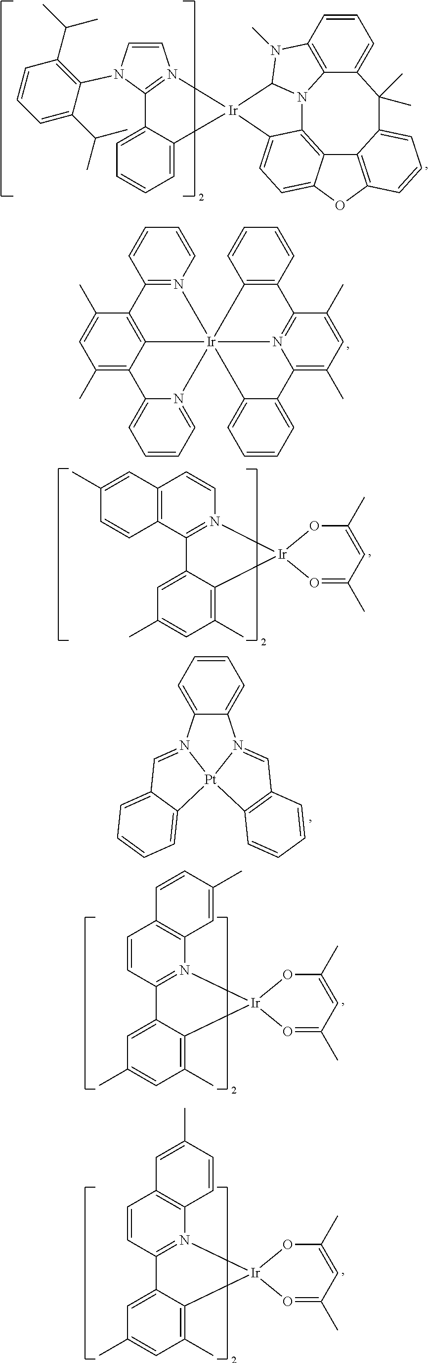
C00105

C00106

C00107
C00108
C00109
C00110
C00111
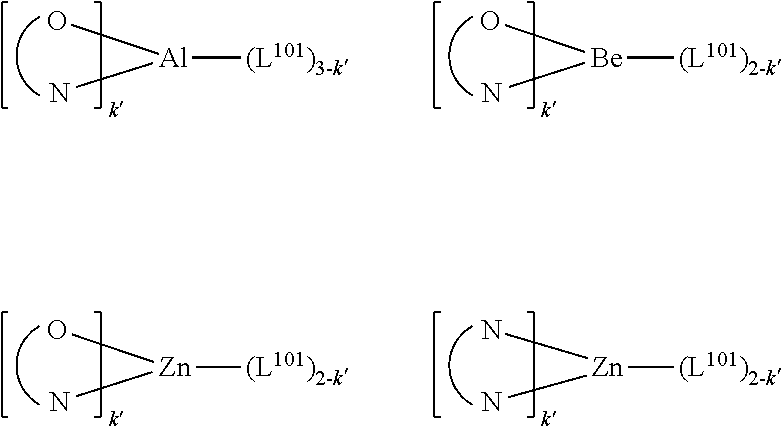
C00112

C00113
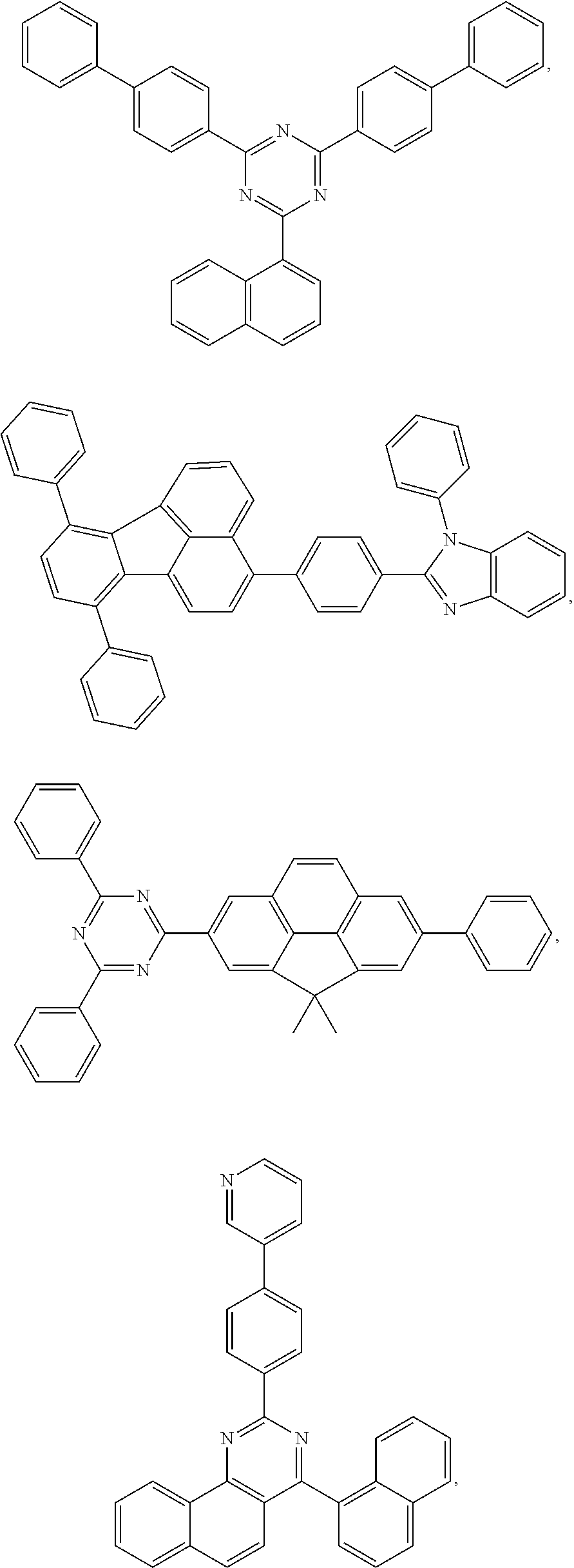
C00114
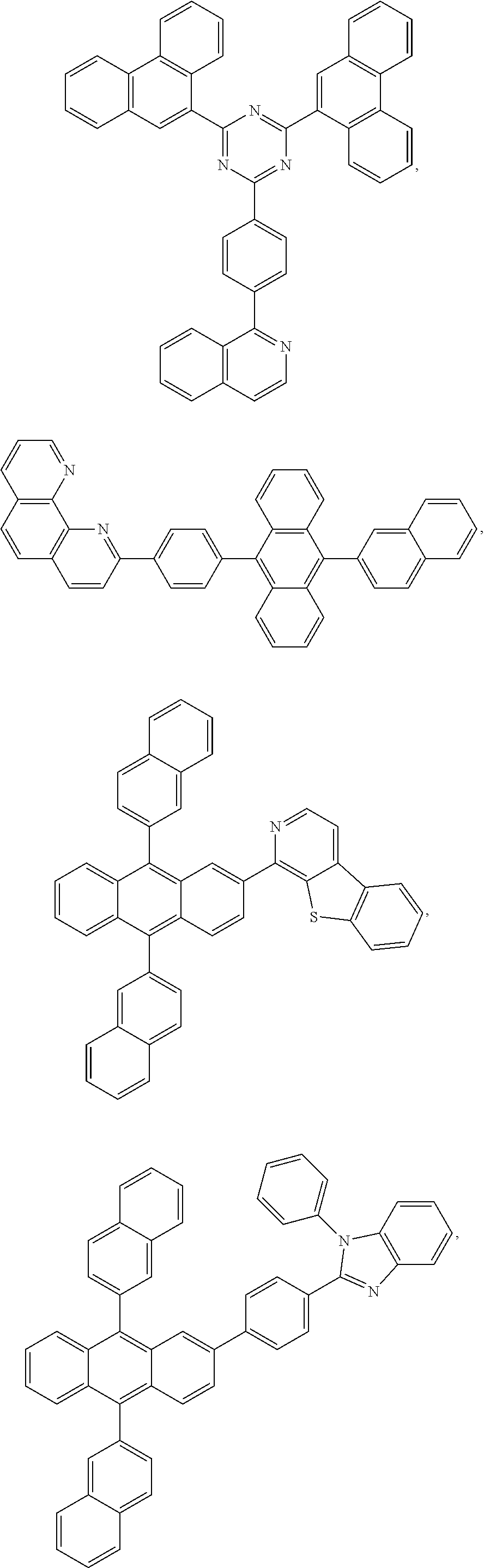
C00115
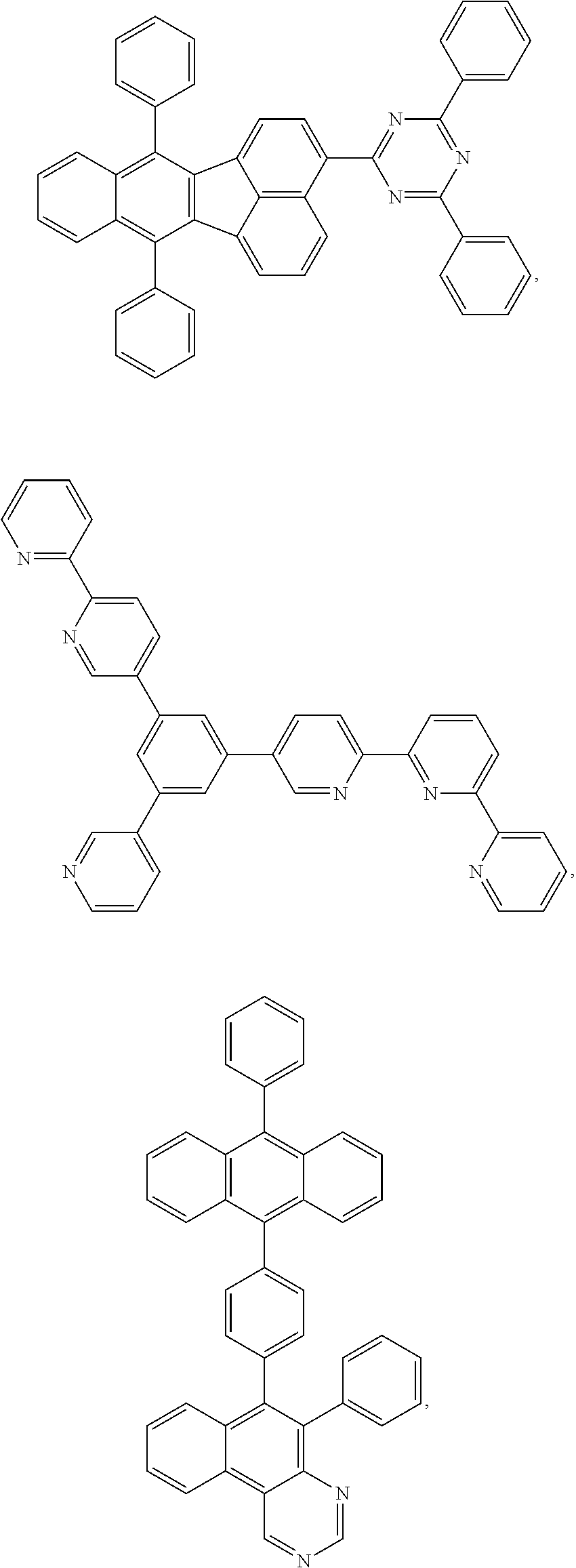
C00116
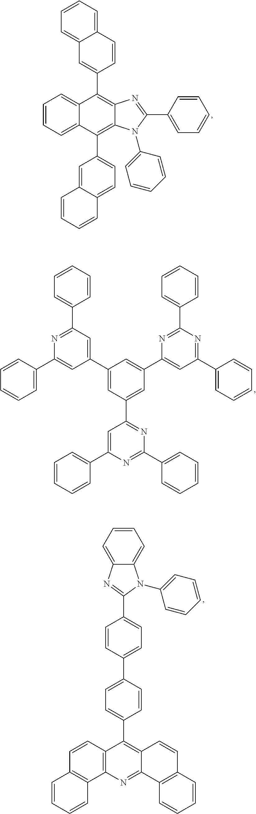
C00117
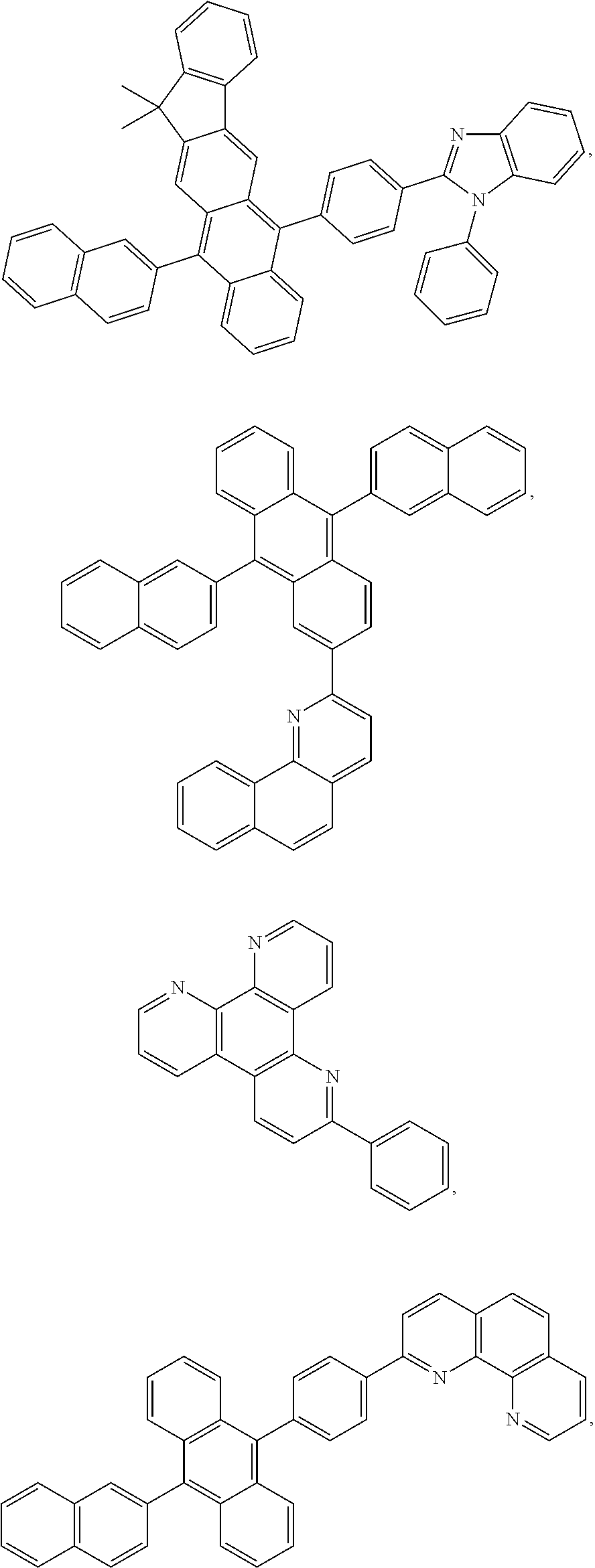
C00118
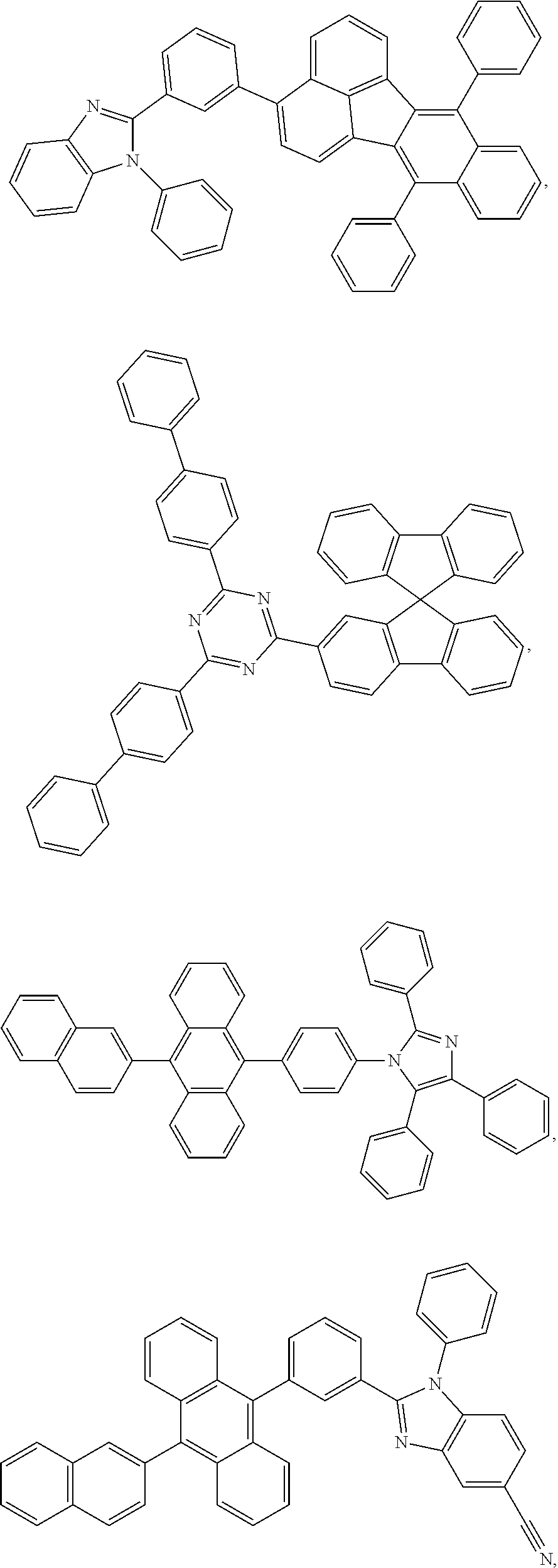
C00119

C00120
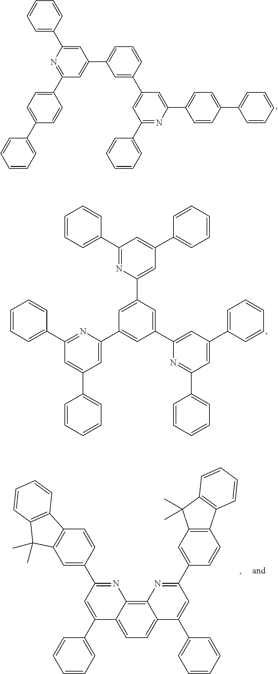
C00121

C00122

C00123
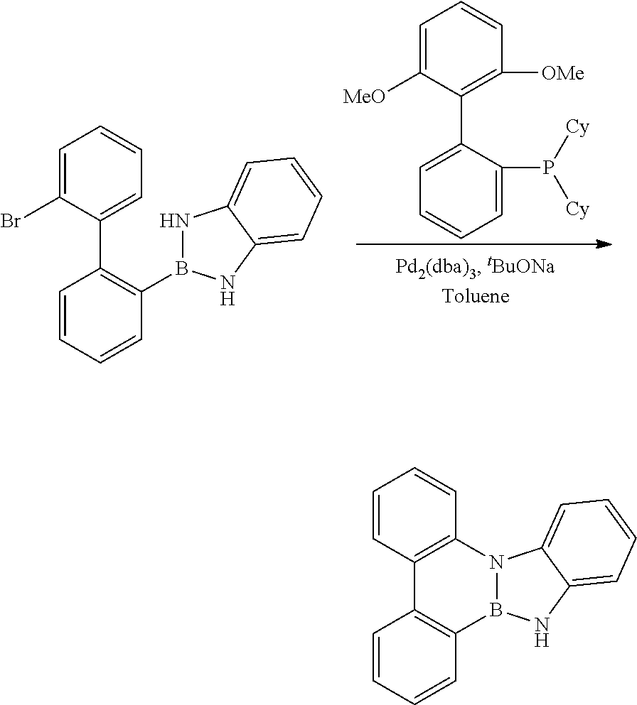
C00124
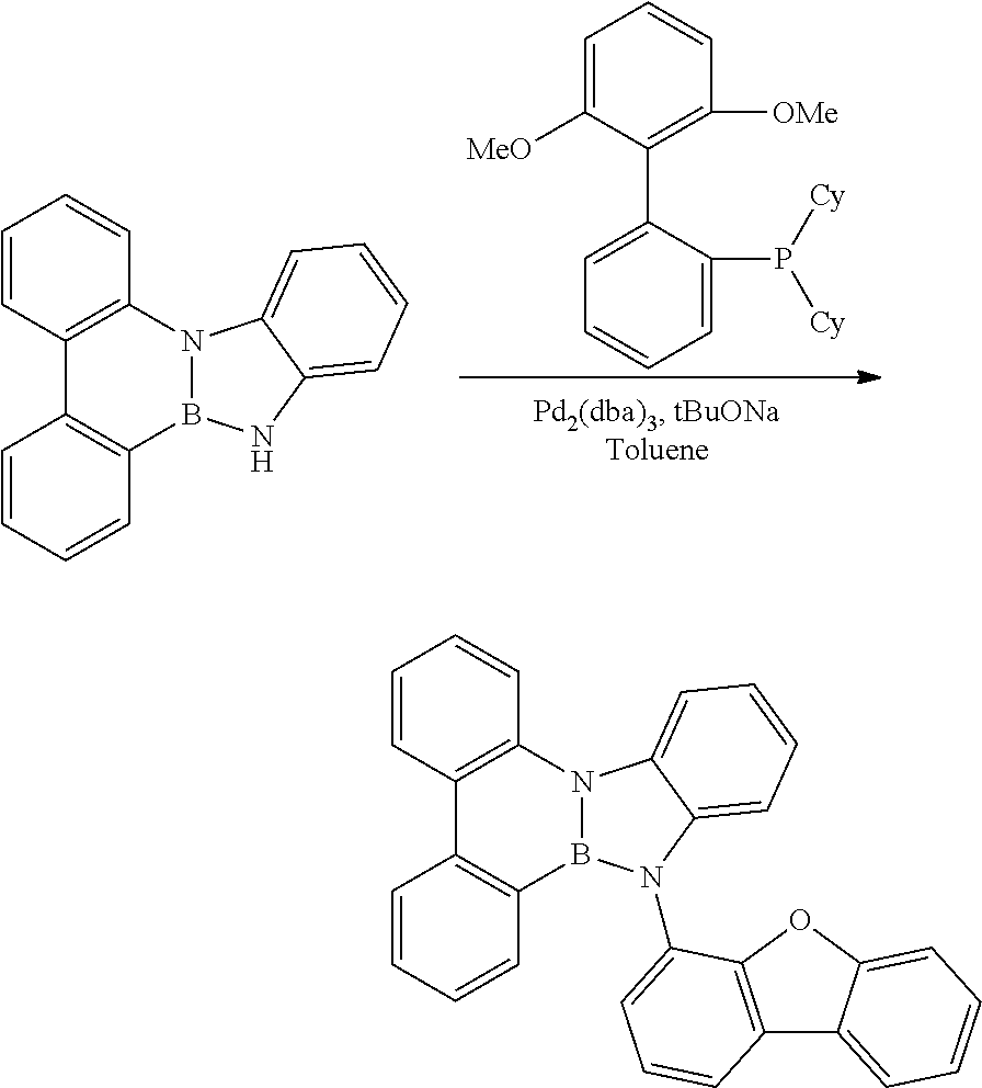
C00125

C00126

C00127

C00128
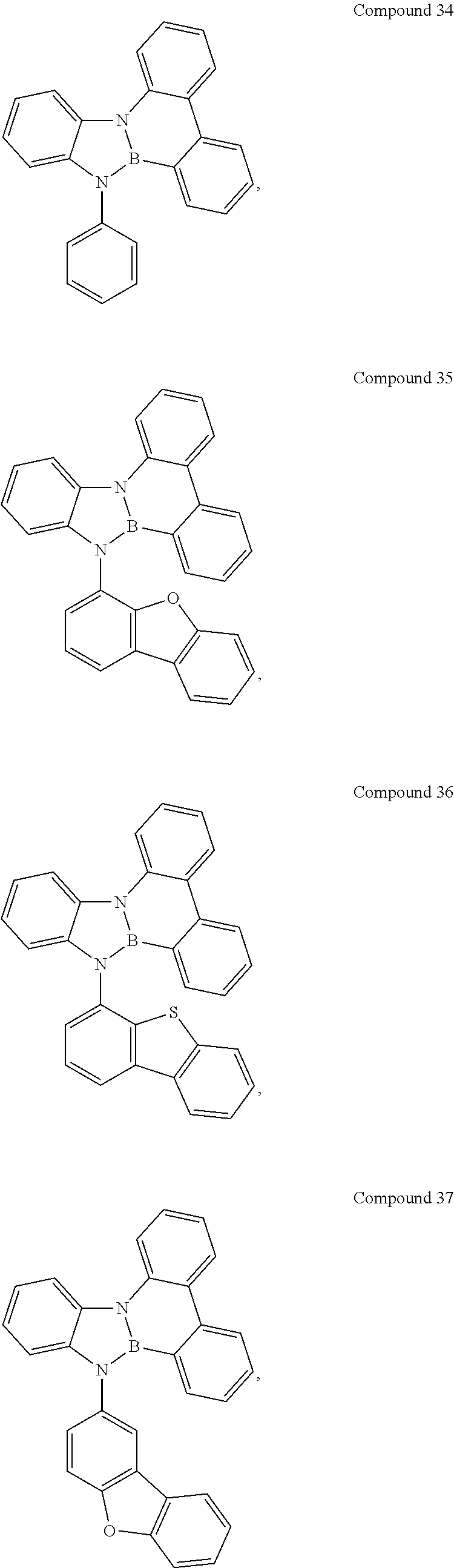
C00129
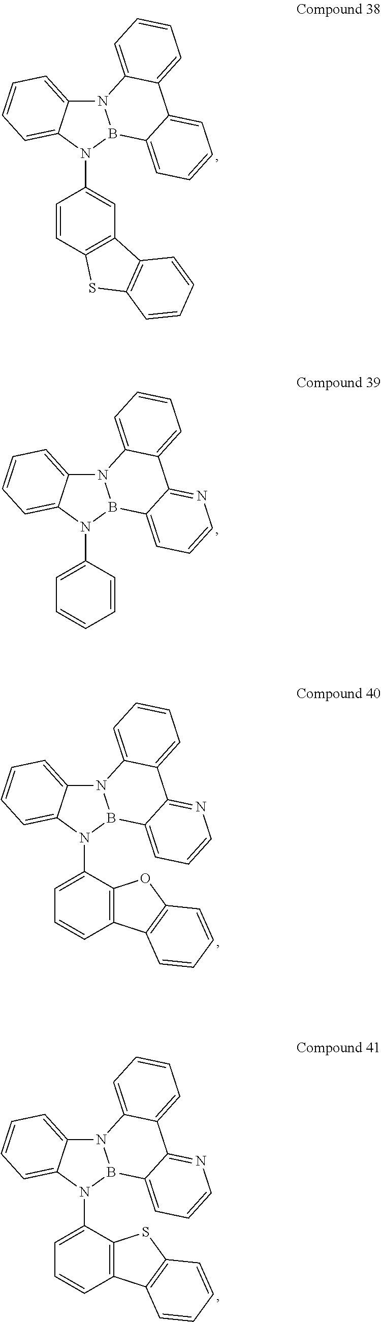
C00130
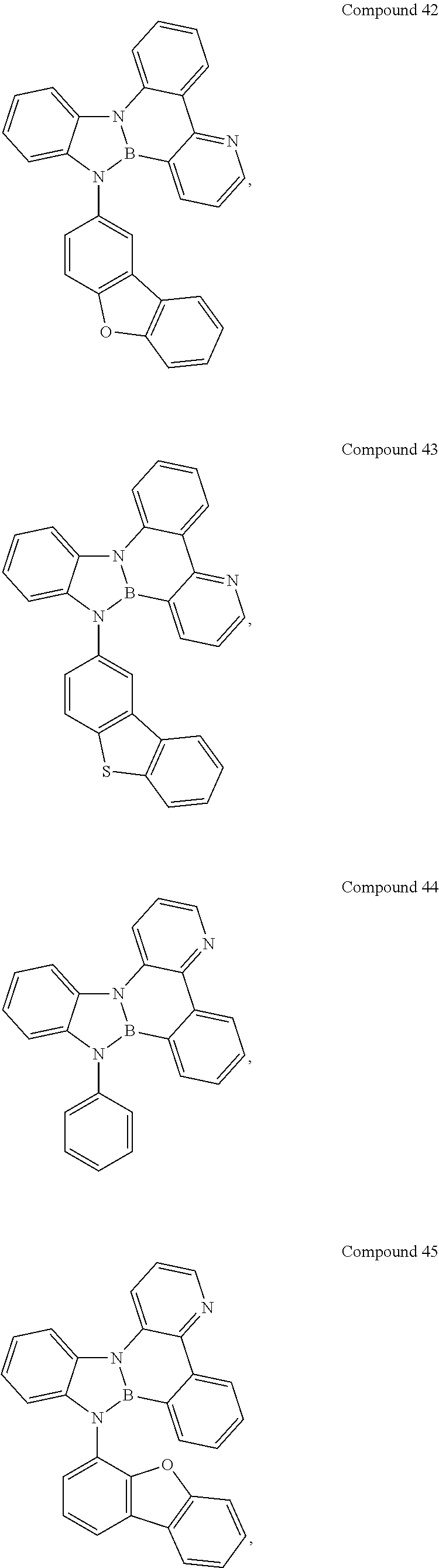
C00131
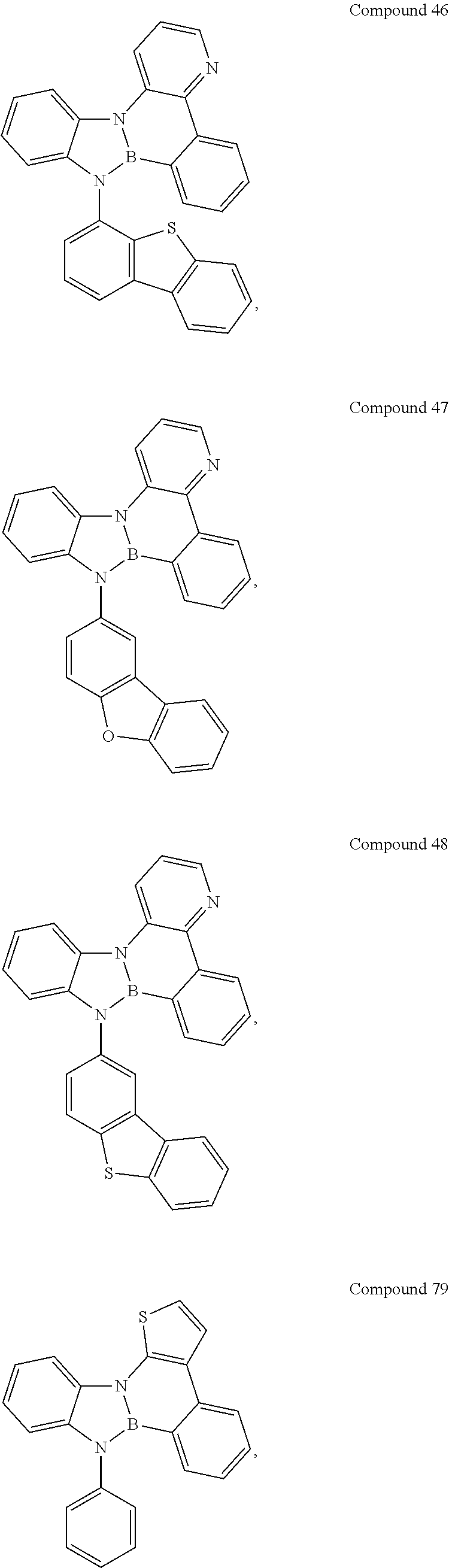
C00132
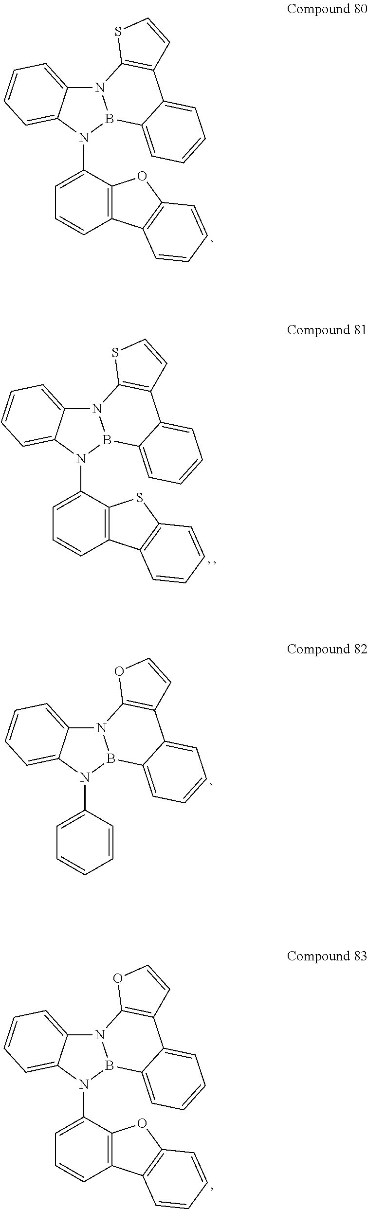
C00133
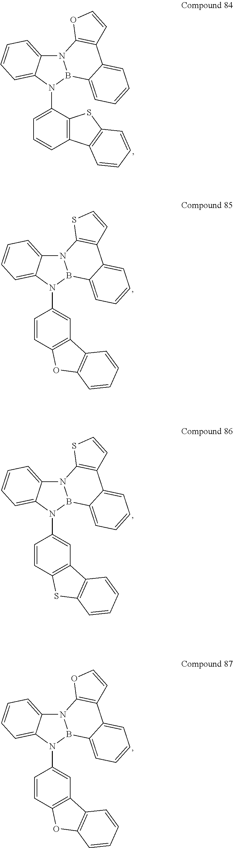
C00134

C00135
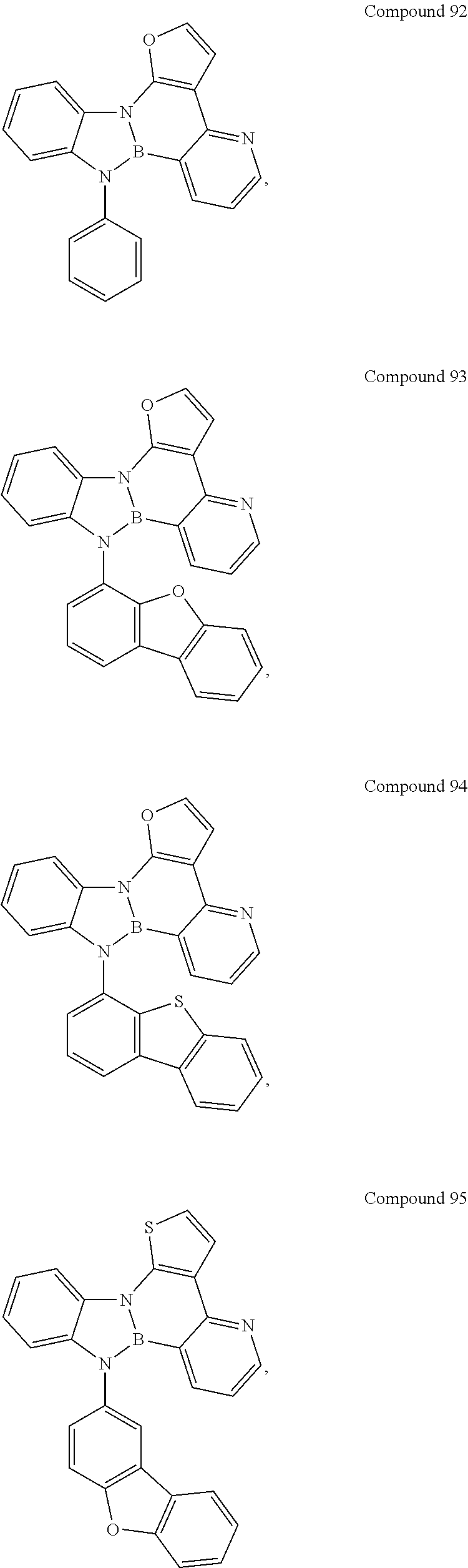
C00136
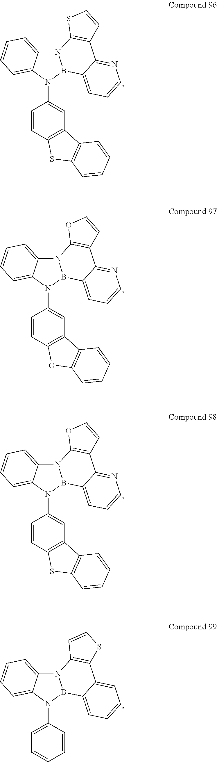
C00137
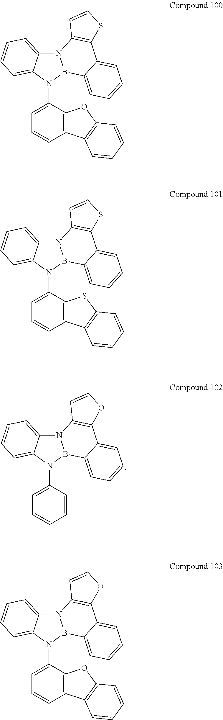
C00138
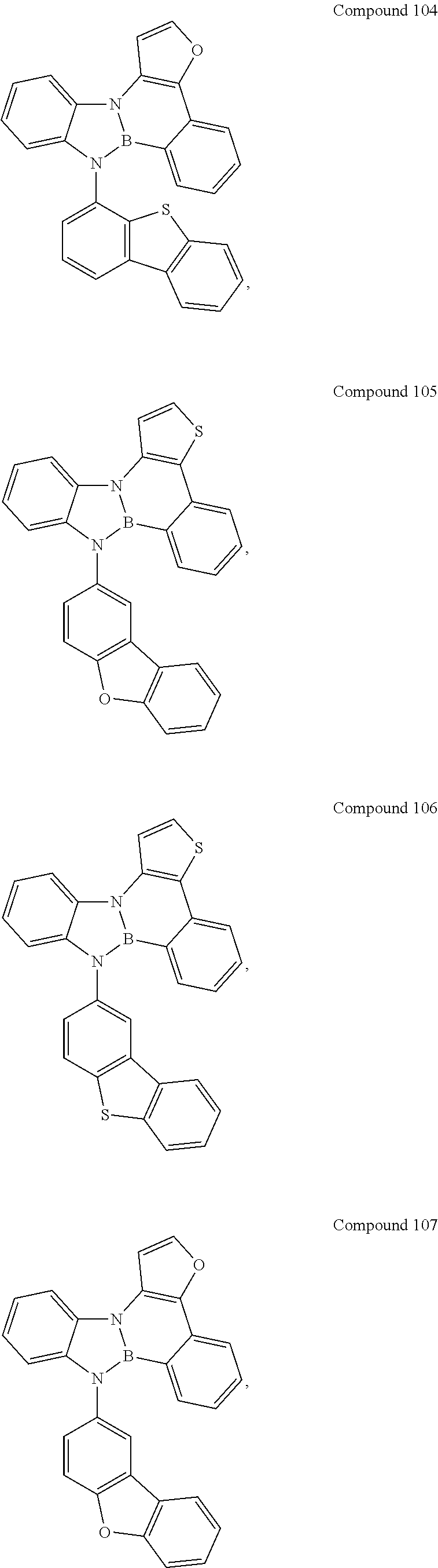
C00139
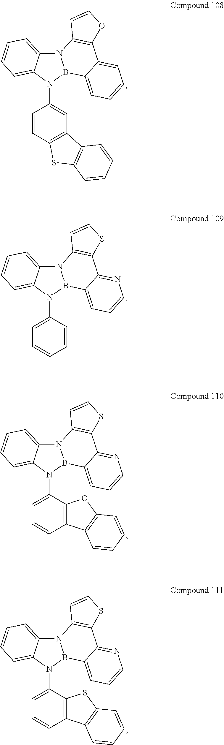
C00140
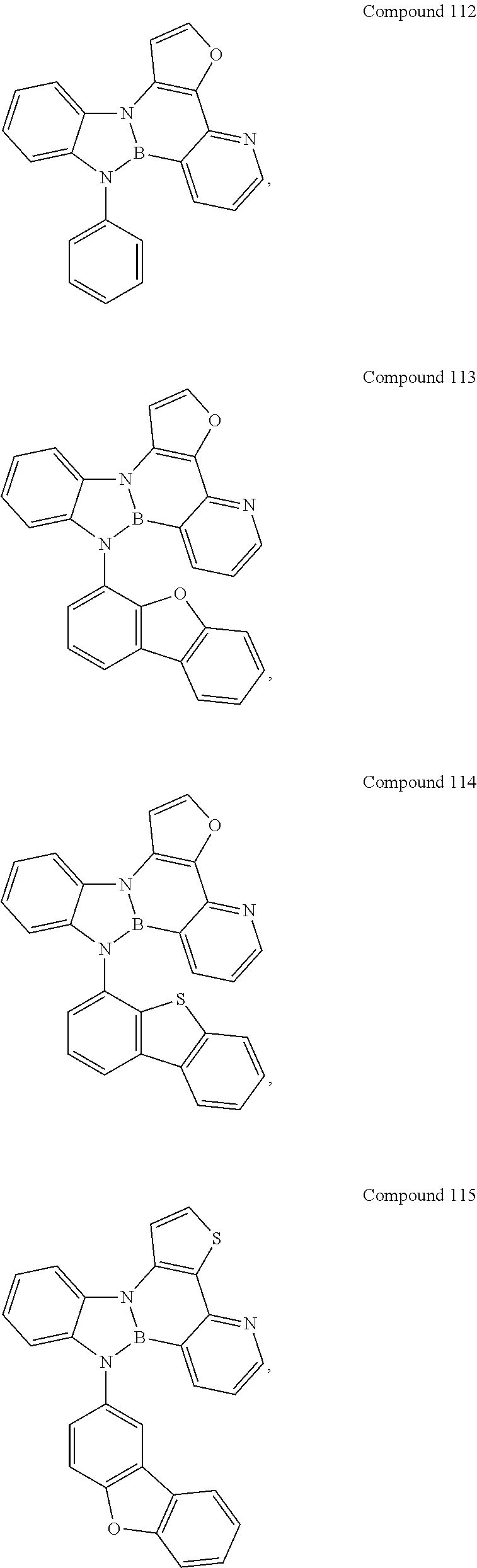
C00141
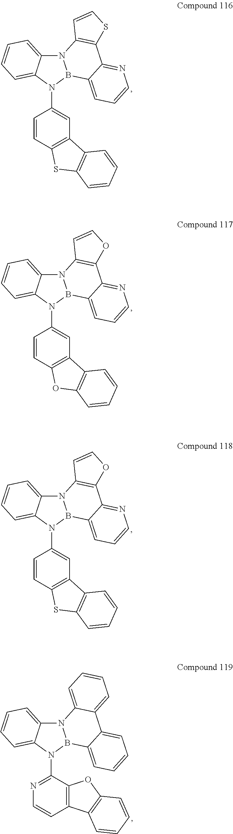
C00142
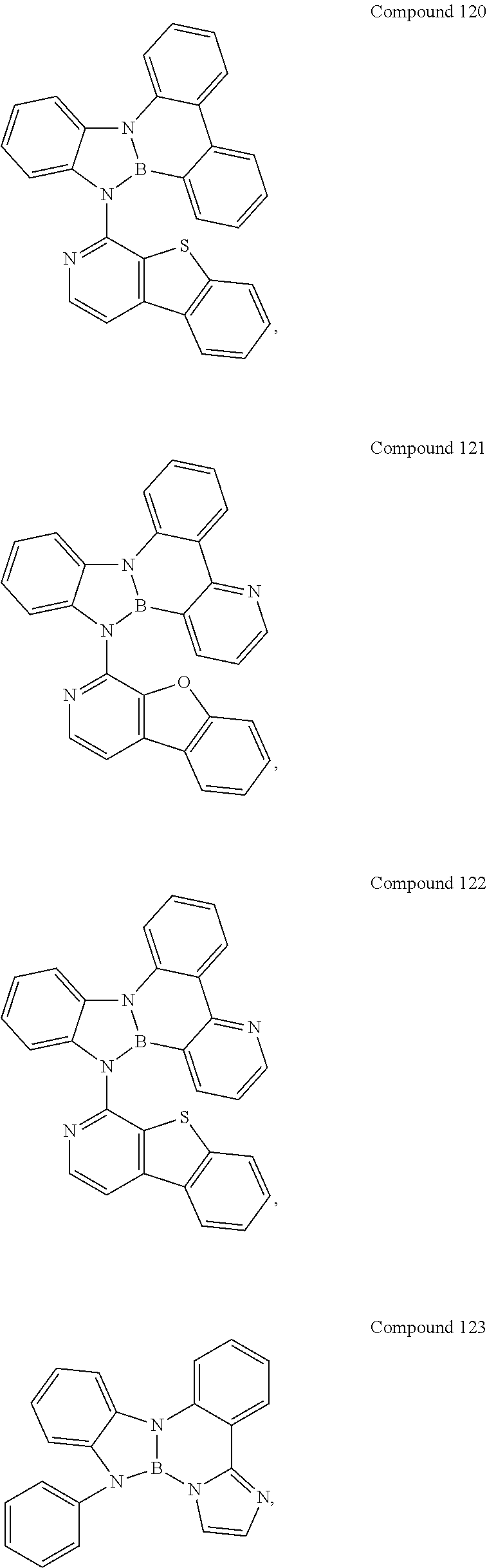
C00143
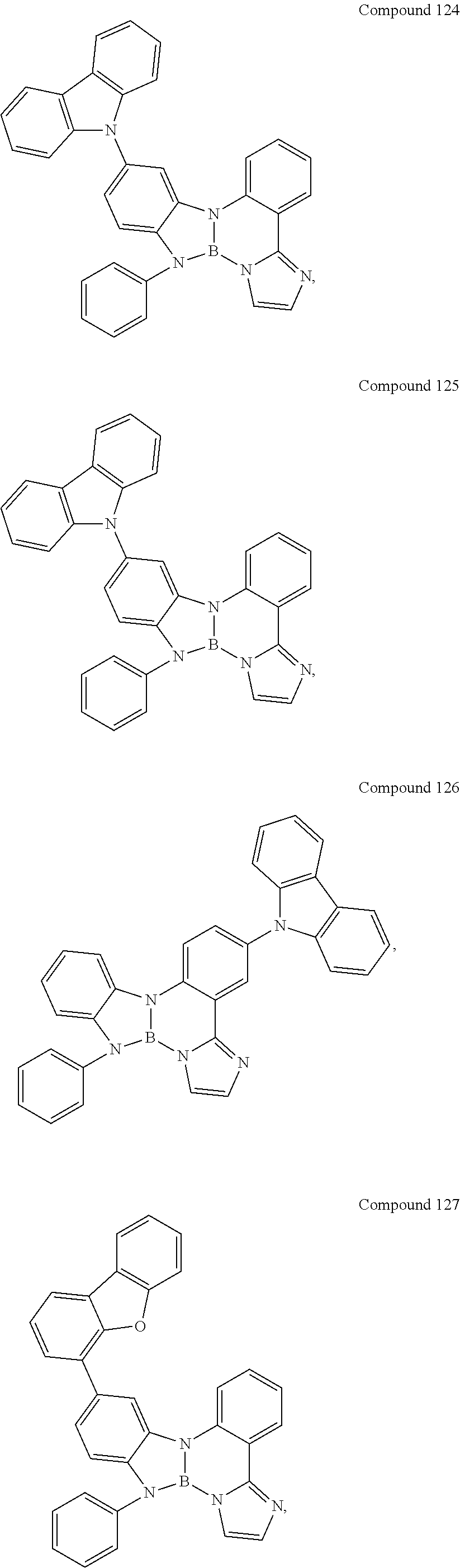
C00144
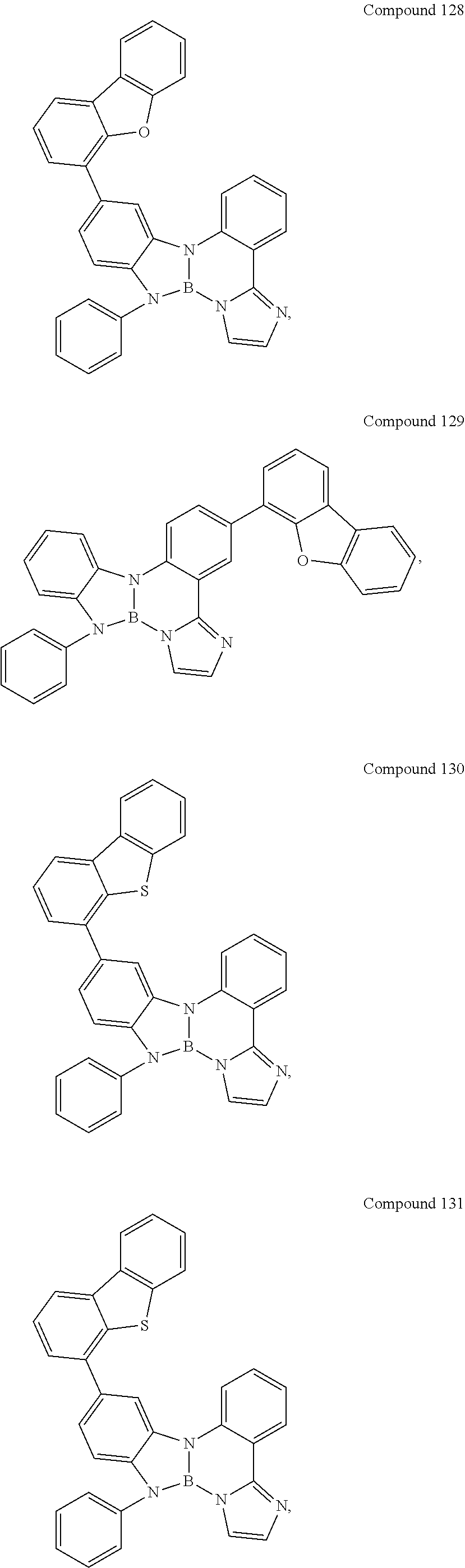
C00145
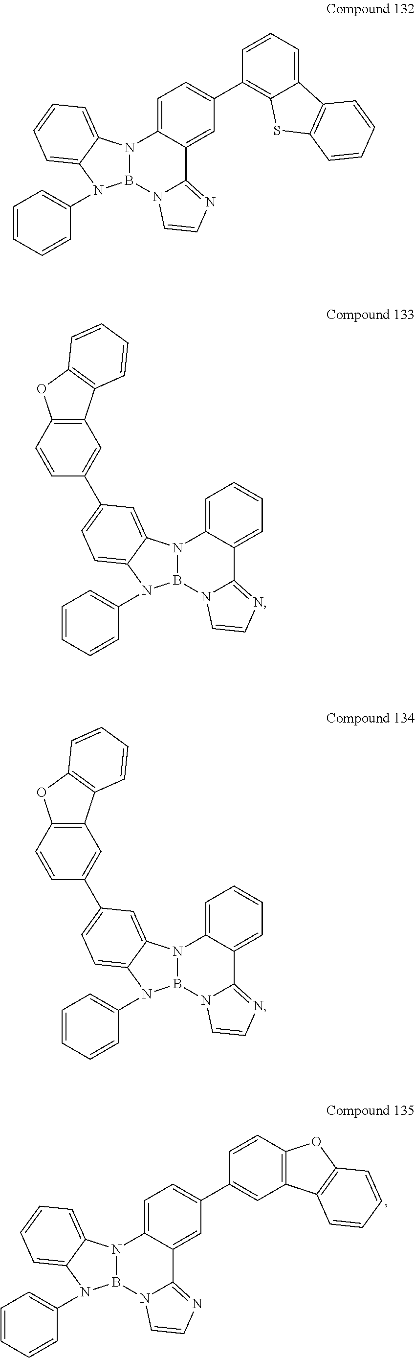
C00146
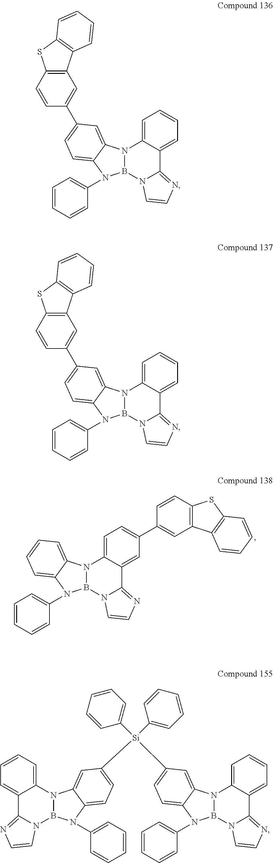
C00147
C00148
C00149
C00150
C00151
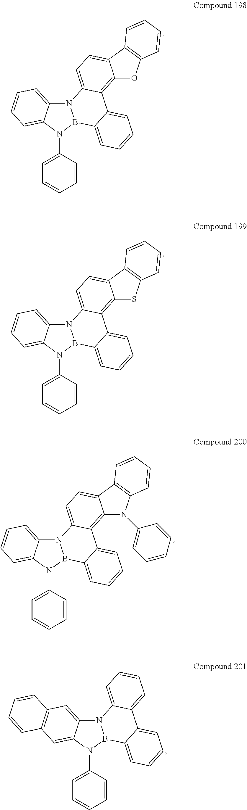
C00152
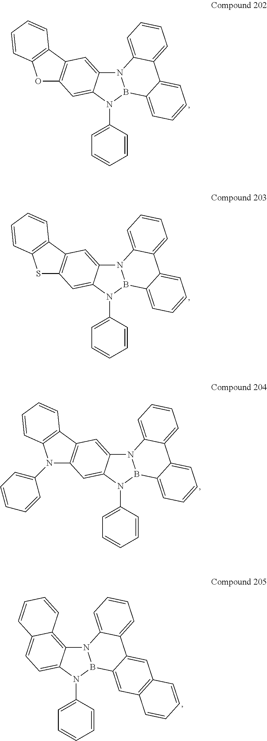
C00153
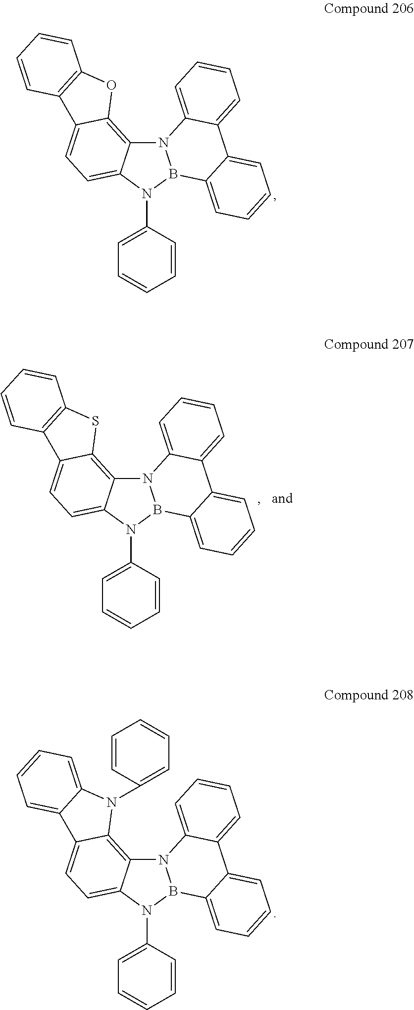
C00154
C00155

C00156
C00157

C00158

C00159

C00160
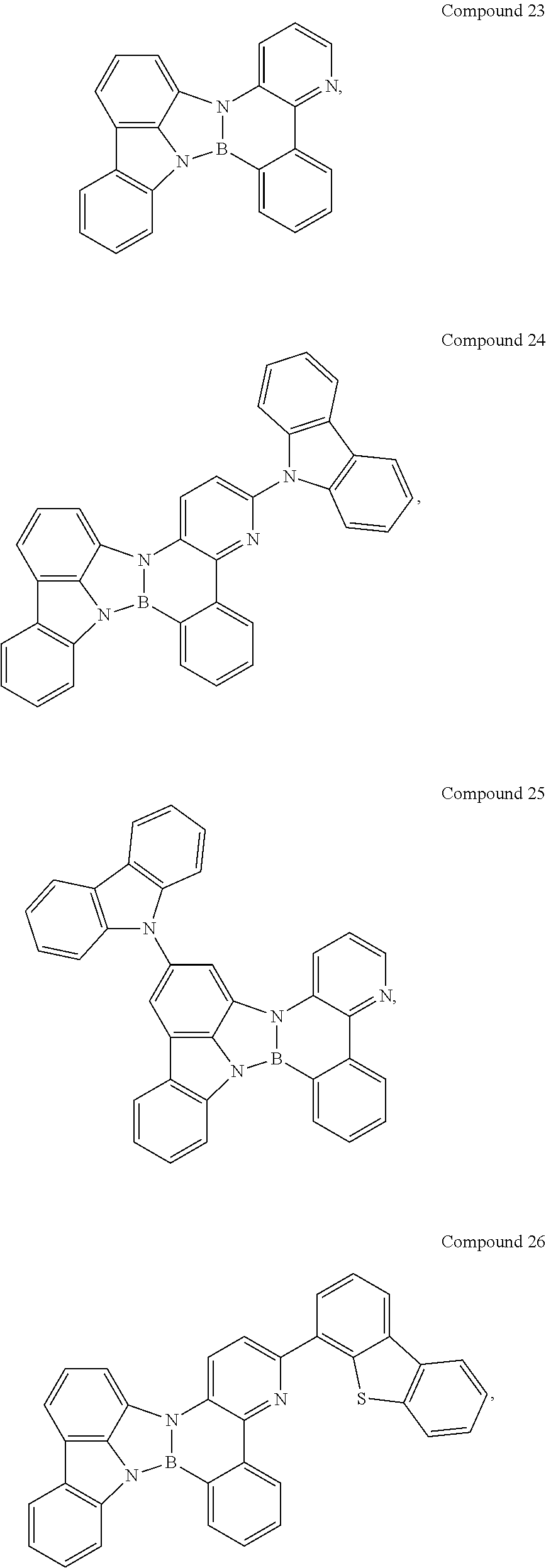
C00161
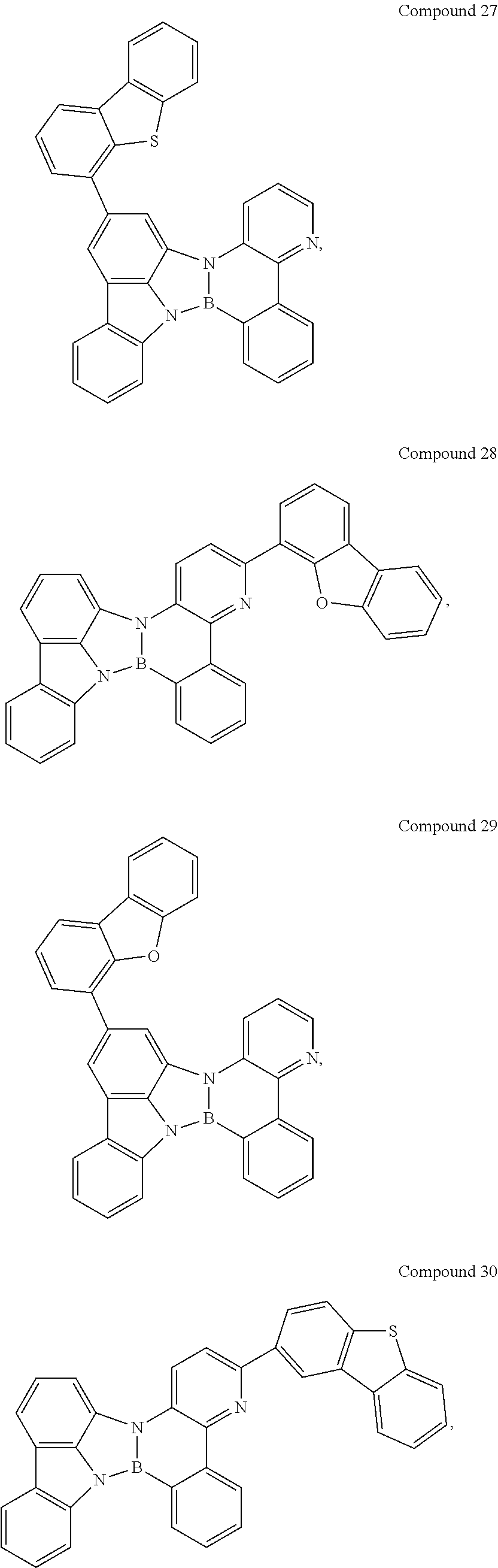
C00162
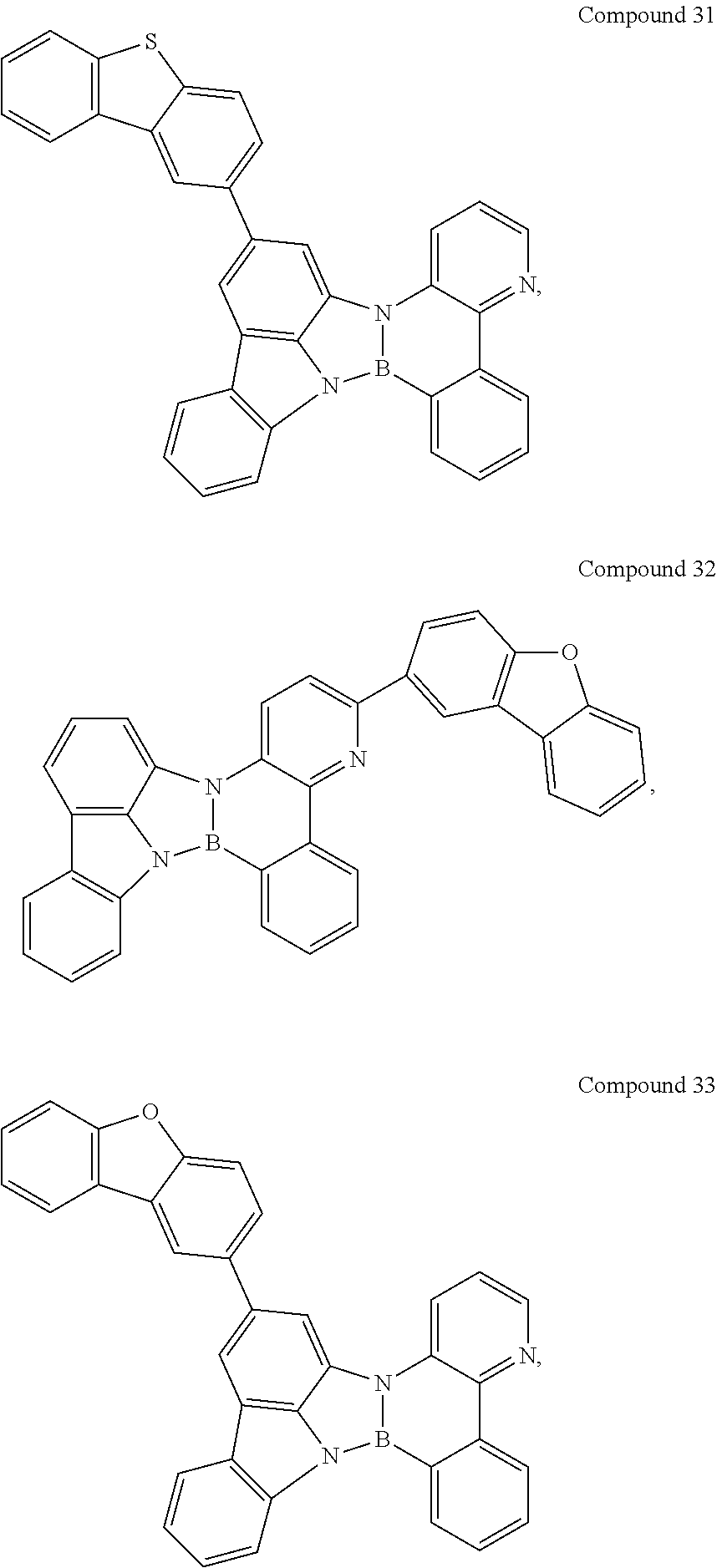
C00163
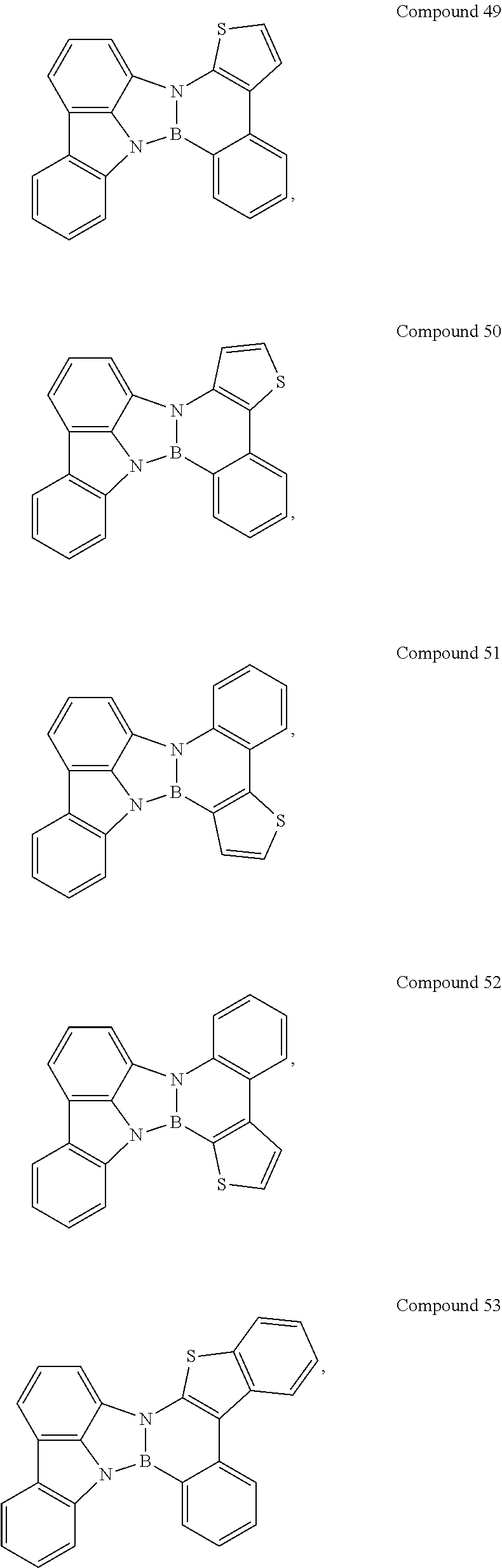
C00164

C00165
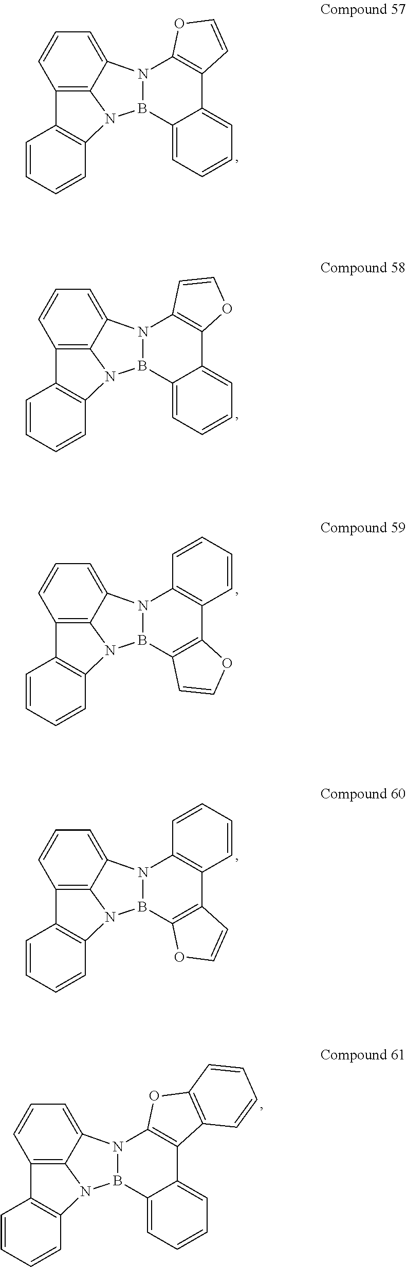
C00166
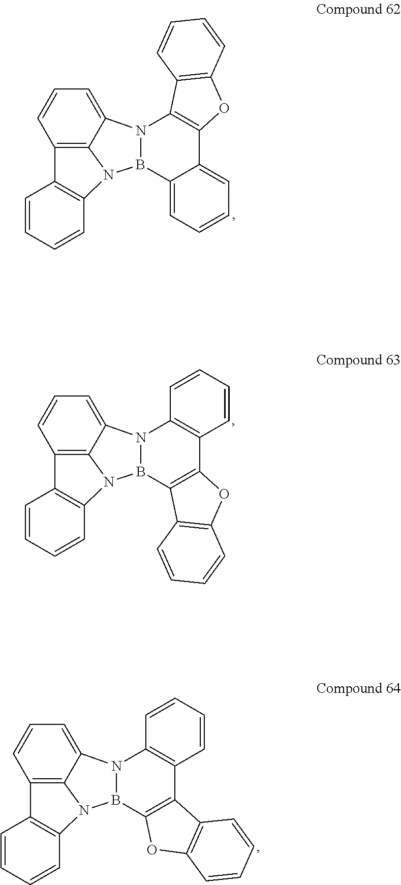
C00167
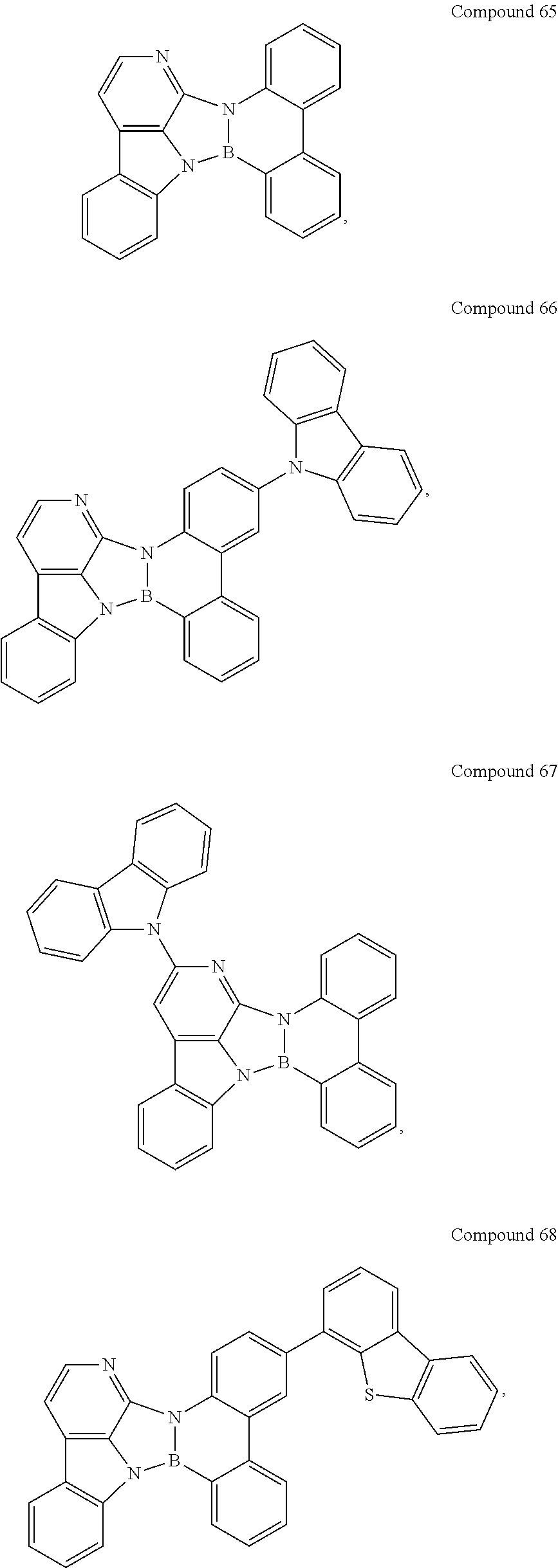
C00168
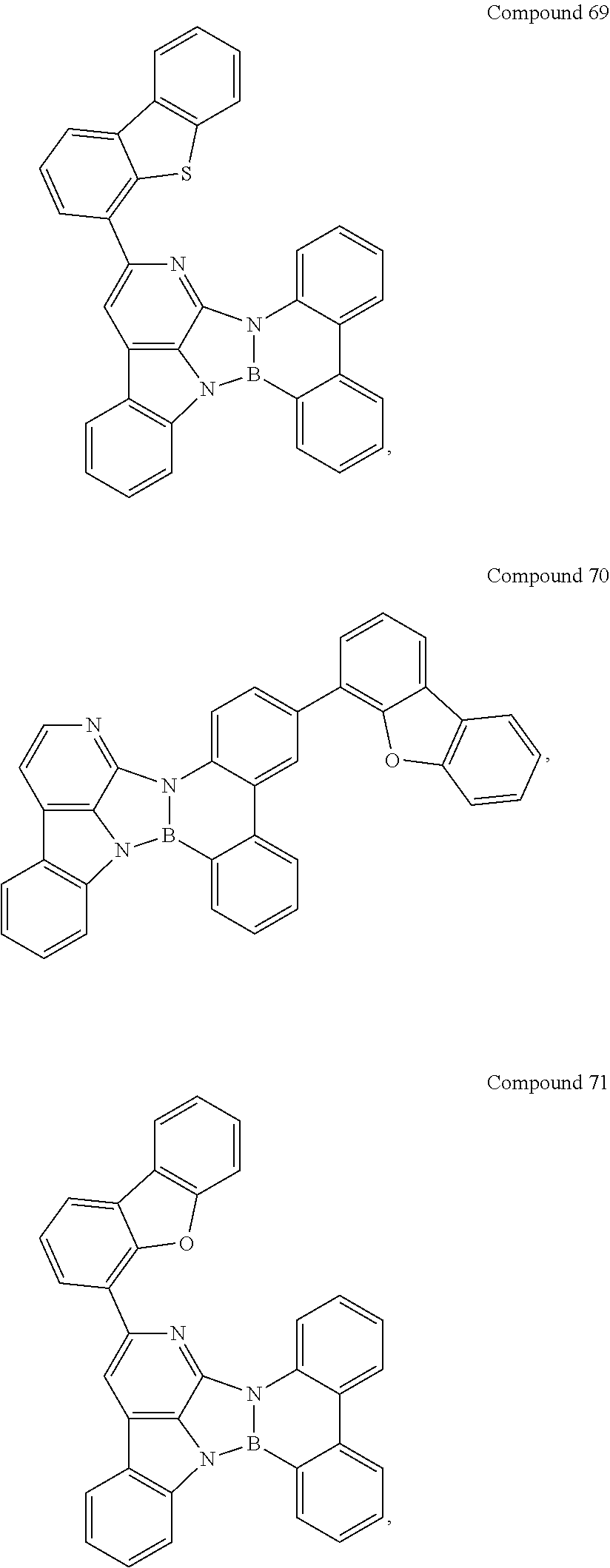
C00169
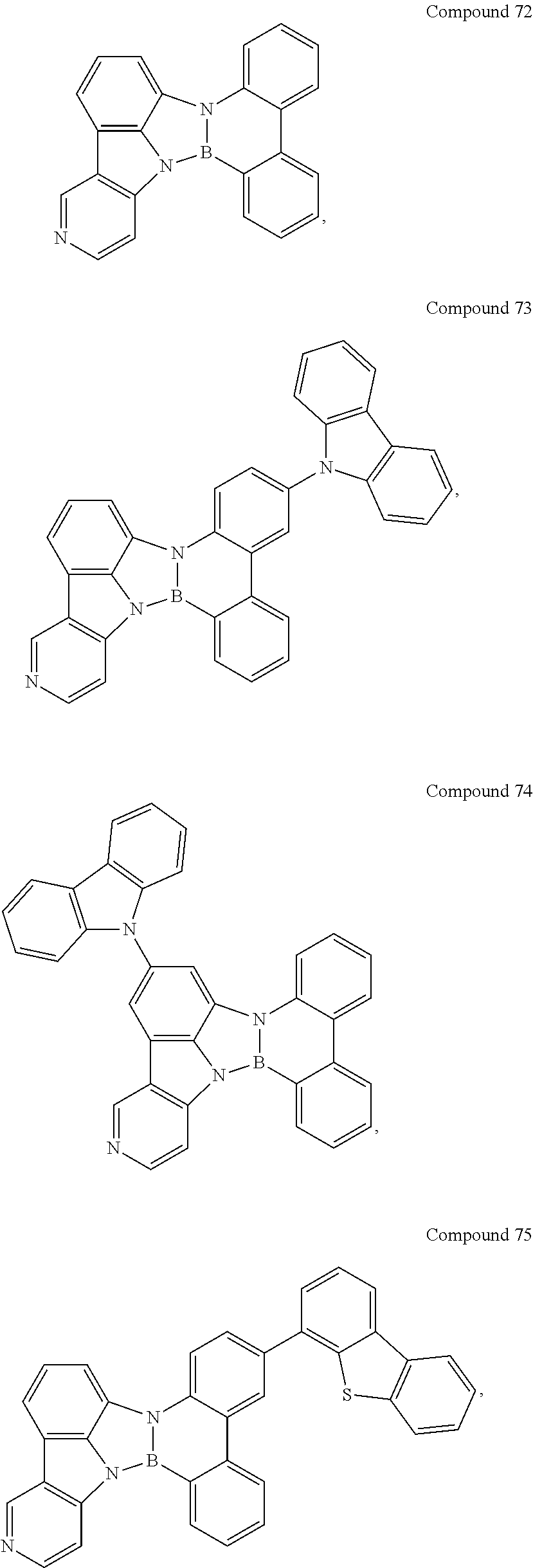
C00170

C00171
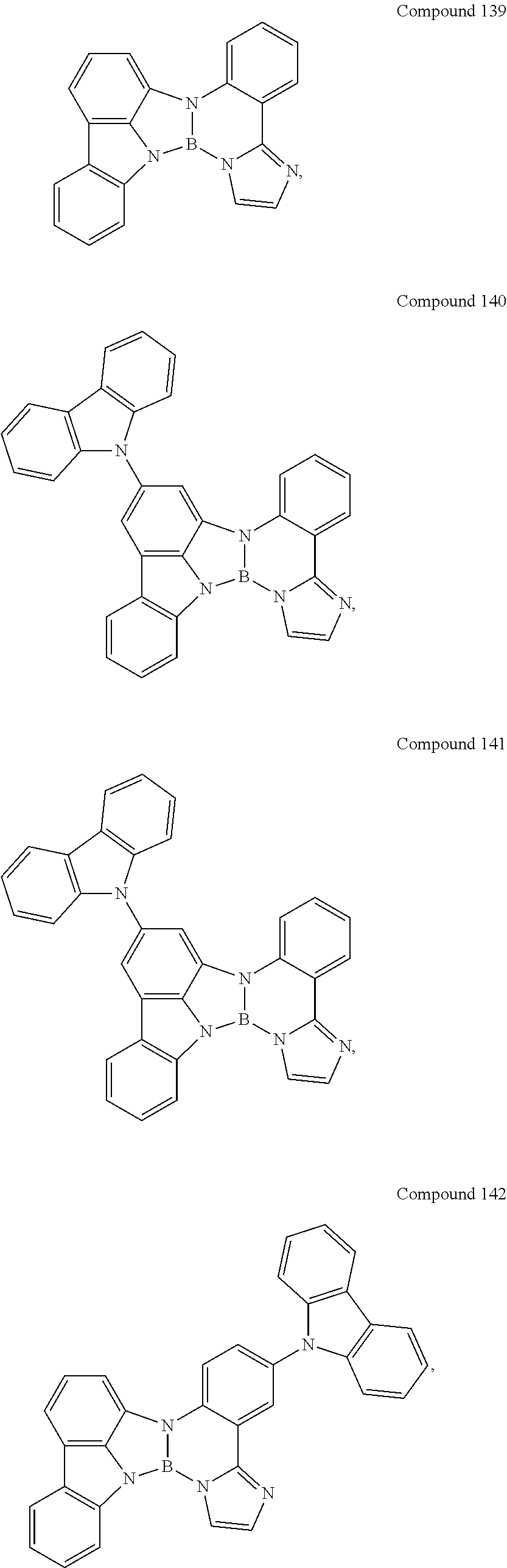
C00172

C00173

C00174

C00175

C00176
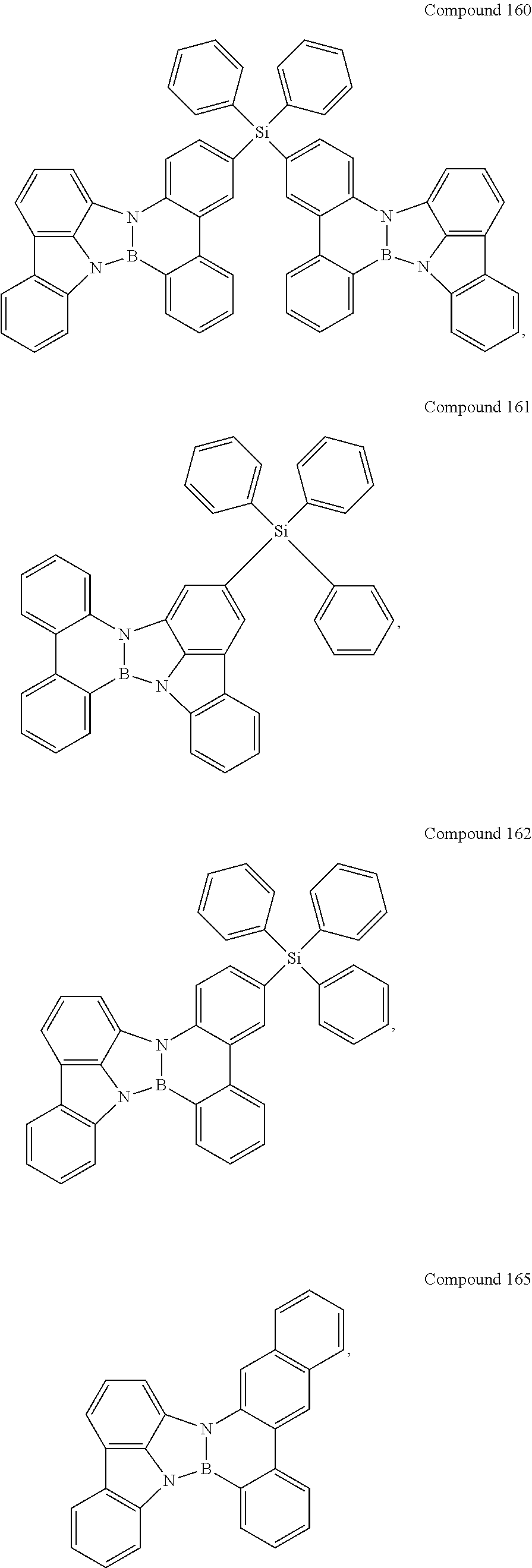
C00177
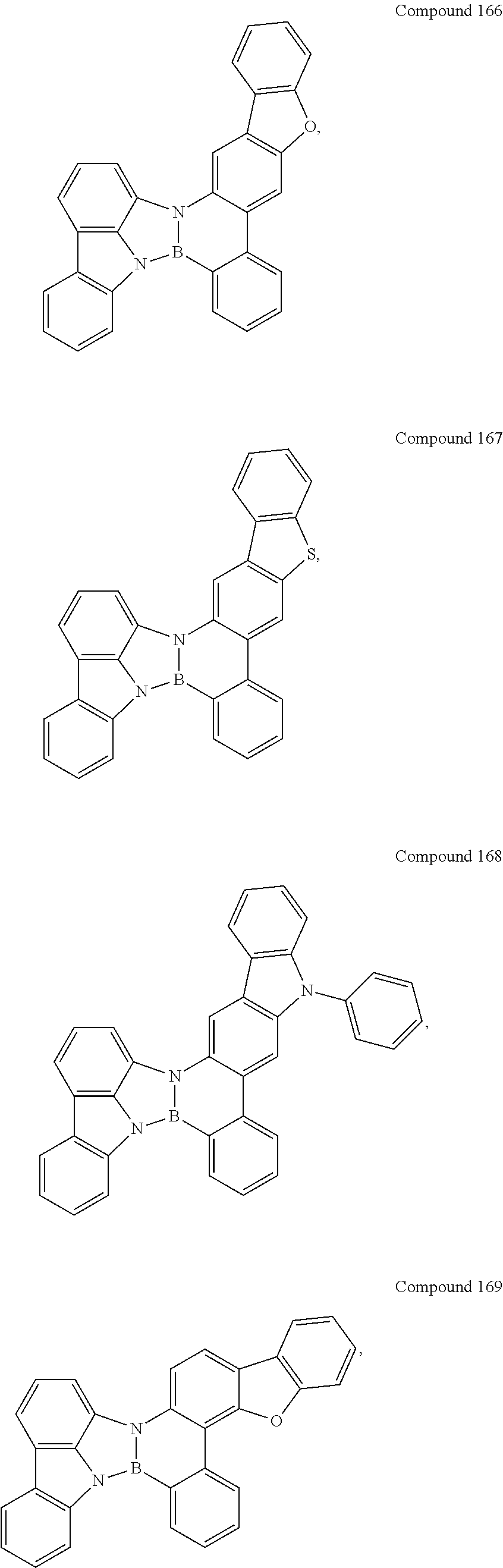
C00178
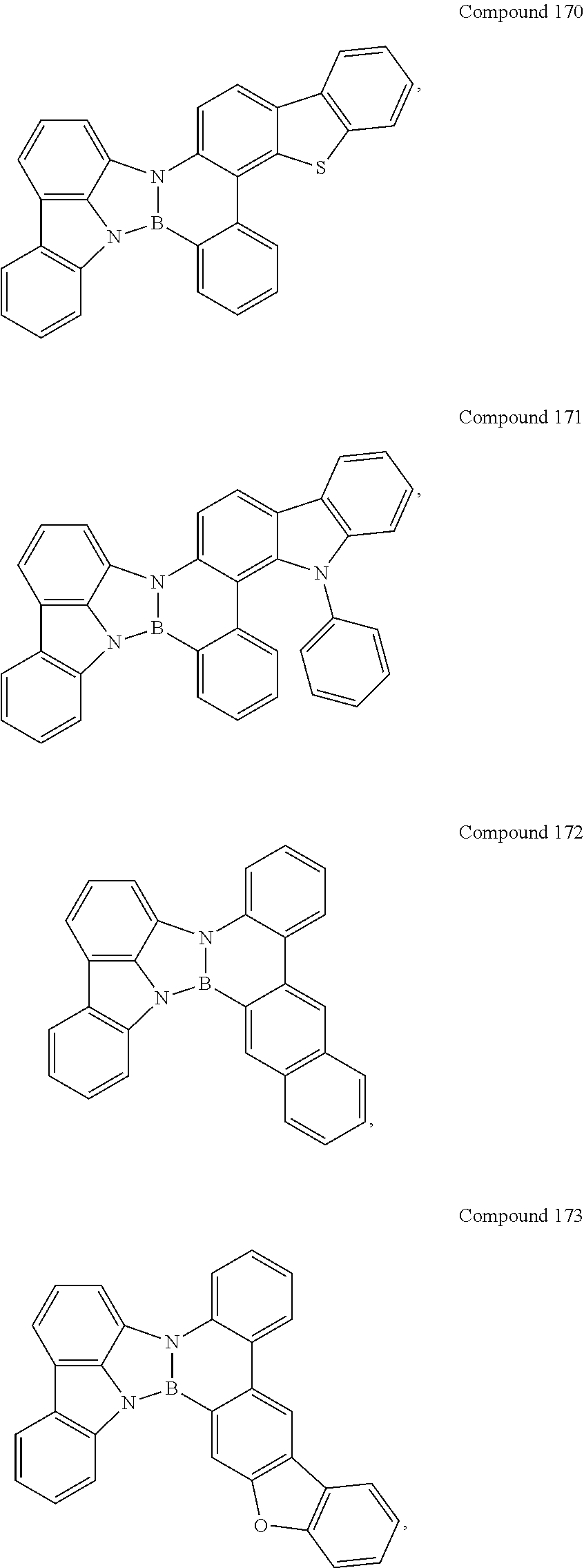
C00179
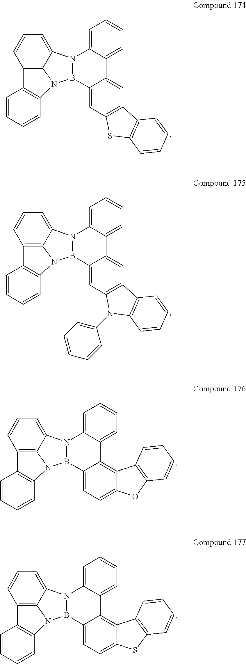
C00180
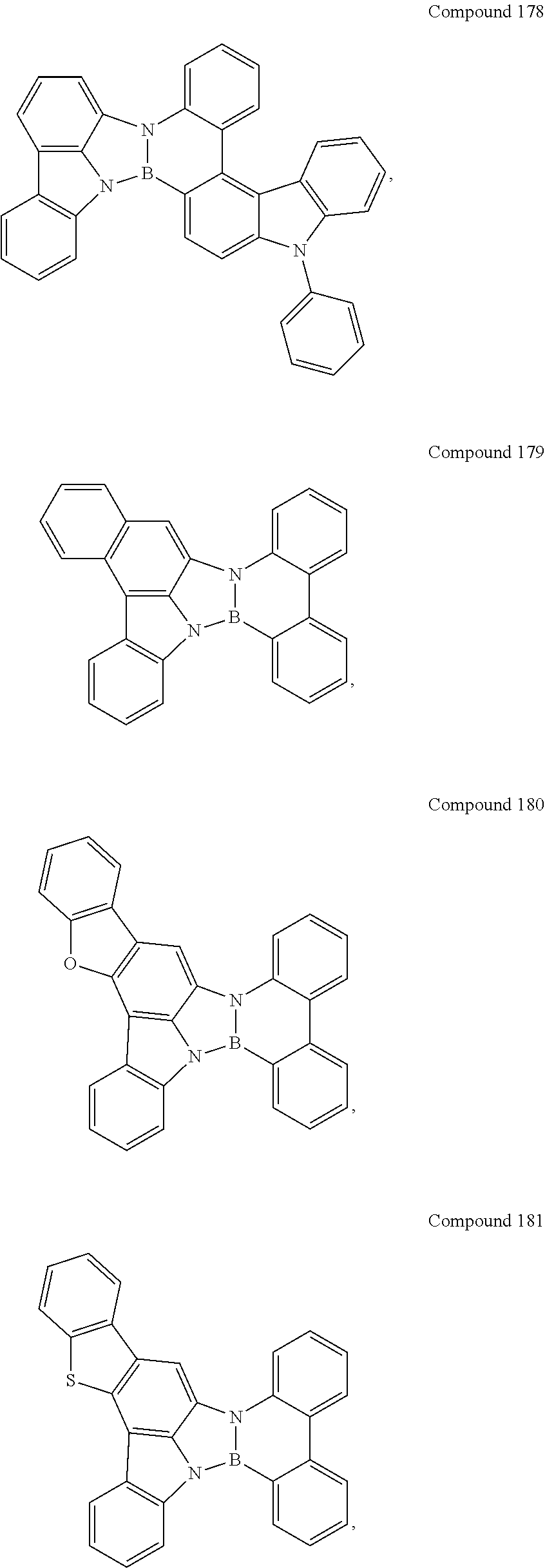
C00181

C00182
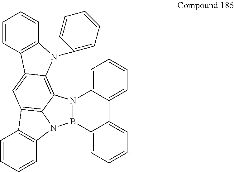
C00183
C00184

C00185
C00186

D00000
D00001
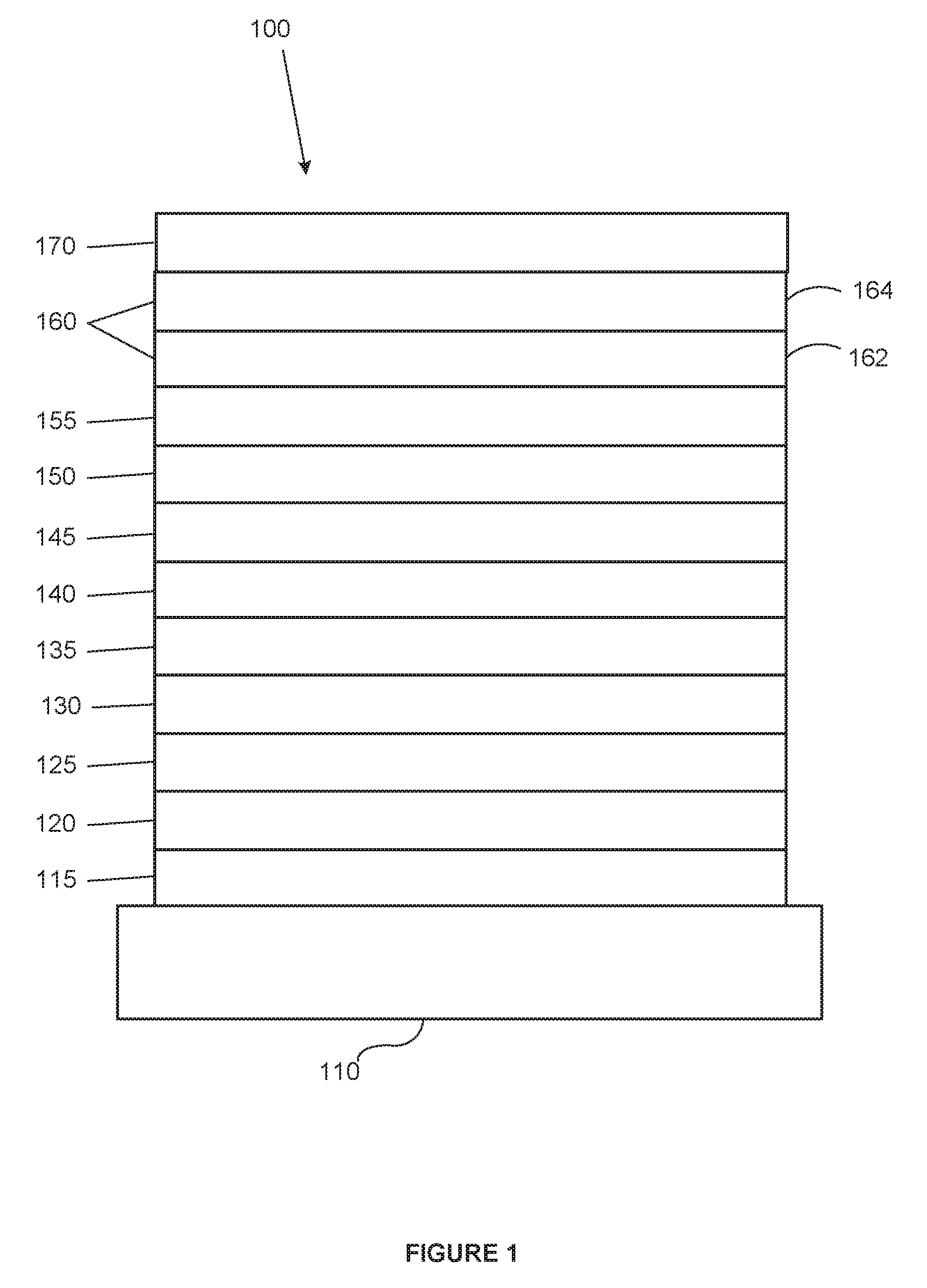
D00002
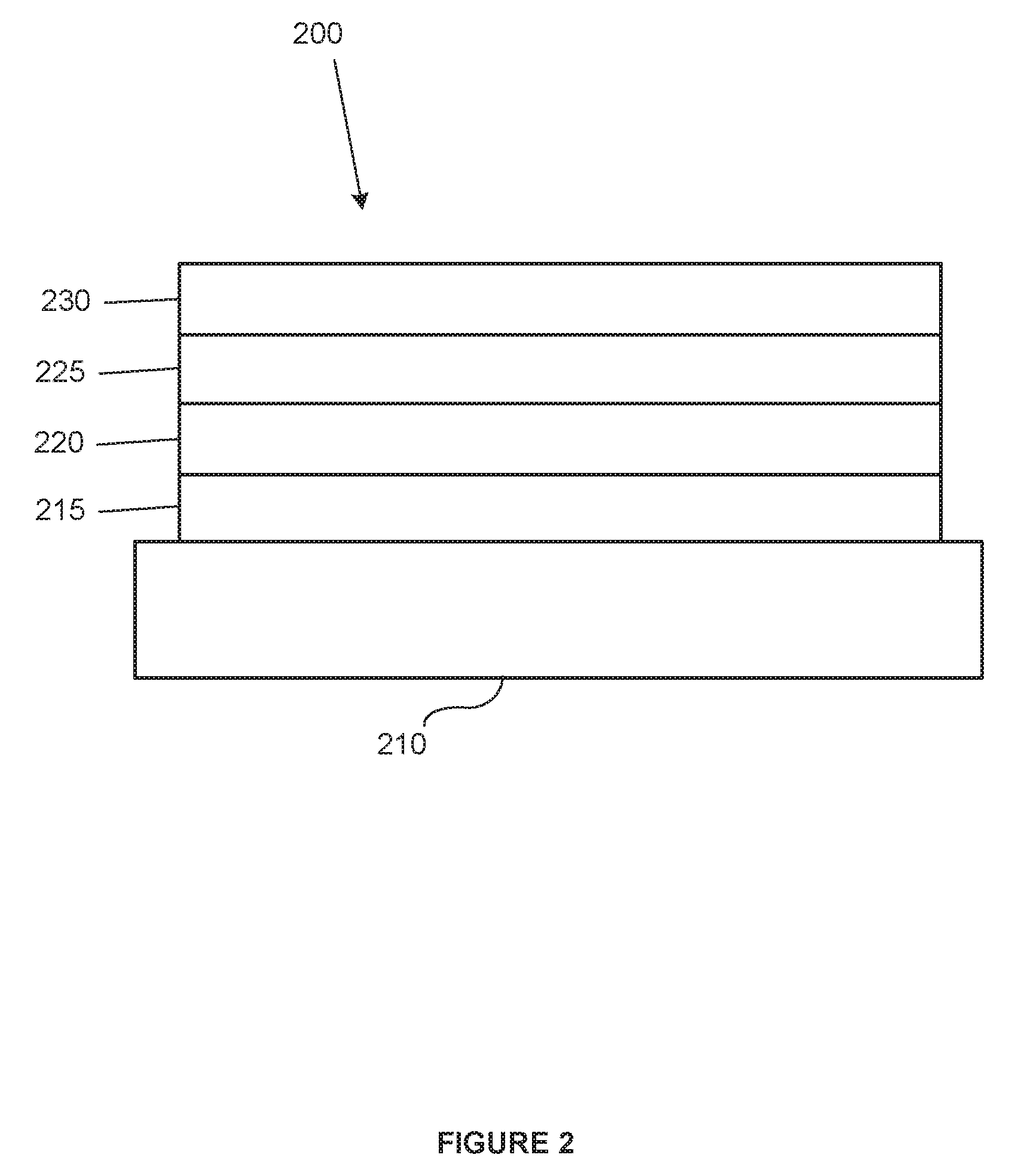
XML
uspto.report is an independent third-party trademark research tool that is not affiliated, endorsed, or sponsored by the United States Patent and Trademark Office (USPTO) or any other governmental organization. The information provided by uspto.report is based on publicly available data at the time of writing and is intended for informational purposes only.
While we strive to provide accurate and up-to-date information, we do not guarantee the accuracy, completeness, reliability, or suitability of the information displayed on this site. The use of this site is at your own risk. Any reliance you place on such information is therefore strictly at your own risk.
All official trademark data, including owner information, should be verified by visiting the official USPTO website at www.uspto.gov. This site is not intended to replace professional legal advice and should not be used as a substitute for consulting with a legal professional who is knowledgeable about trademark law.