Sense electrode design
Yilmaz
U.S. patent number 10,338,759 [Application Number 16/277,636] was granted by the patent office on 2019-07-02 for sense electrode design. This patent grant is currently assigned to NEODRON LIMITED. The grantee listed for this patent is Neodron Limited. Invention is credited to Esat Yilmaz.


| United States Patent | 10,338,759 |
| Yilmaz | July 2, 2019 |
Sense electrode design
Abstract
A touch sensitive device includes a plurality of sense electrodes arranged in a pattern to receive charge from drive electrodes. The pattern of sense electrodes has extreme portions having worst case charge transfer times, wherein the worst case charge transfer time at multiple extreme portions is substantially equal.
| Inventors: | Yilmaz; Esat (Santa Cruz, CA) | ||||||||||
|---|---|---|---|---|---|---|---|---|---|---|---|
| Applicant: |
|
||||||||||
| Assignee: | NEODRON LIMITED (Dublin,
IE) |
||||||||||
| Family ID: | 43897999 | ||||||||||
| Appl. No.: | 16/277,636 | ||||||||||
| Filed: | February 15, 2019 |
Related U.S. Patent Documents
| Application Number | Filing Date | Patent Number | Issue Date | ||
|---|---|---|---|---|---|
| 15915726 | Mar 8, 2018 | 10228808 | |||
| 12605779 | Mar 13, 2018 | 9916045 | |||
| Current U.S. Class: | 1/1 |
| Current CPC Class: | G06F 3/0443 (20190501); G06F 3/044 (20130101); G06F 3/0446 (20190501); Y10T 29/49002 (20150115) |
| Current International Class: | G06F 3/044 (20060101) |
References Cited [Referenced By]
U.S. Patent Documents
| 5083118 | January 1992 | Kazama |
| 6297811 | October 2001 | Kent et al. |
| 6522047 | February 2003 | Toda |
| 7129935 | October 2006 | Mackey |
| 7151528 | December 2006 | Taylor |
| 7382139 | June 2008 | Mackey |
| 7548073 | June 2009 | Mackey |
| 7589713 | September 2009 | Sato |
| 7663607 | February 2010 | Hotelling et al. |
| 7808255 | October 2010 | Hristov et al. |
| 7864160 | January 2011 | Geaghan |
| 7864503 | January 2011 | Chang |
| 7875814 | January 2011 | Chen et al. |
| 7920129 | April 2011 | Hotelling et al. |
| 8004499 | August 2011 | Geaghan |
| 8031094 | October 2011 | Hotelling et al. |
| 8031174 | October 2011 | Hamblin et al. |
| 8040326 | October 2011 | Hotelling et al. |
| 8049732 | November 2011 | Hotelling et al. |
| 8179381 | May 2012 | Frey et al. |
| 8217902 | July 2012 | Chang et al. |
| 8502796 | August 2013 | Yilmaz |
| 8593425 | November 2013 | Hong et al. |
| 8599150 | December 2013 | Philipp |
| 8638112 | January 2014 | Day |
| 8665236 | March 2014 | Myers |
| 8692799 | April 2014 | Landry et al. |
| 8786572 | July 2014 | Yilmaz |
| 8797290 | August 2014 | Yilmaz |
| 8823653 | September 2014 | Matsuo |
| 8830180 | September 2014 | Yilmaz et al. |
| 8860690 | October 2014 | Trend et al. |
| 8901944 | December 2014 | Chai |
| 8970523 | March 2015 | Lin et al. |
| 9116582 | August 2015 | Mohindra et al. |
| 9372579 | June 2016 | Philipp |
| 9425790 | August 2016 | Stone |
| 9436324 | September 2016 | Singh et al. |
| 9436328 | September 2016 | Trend et al. |
| 9626045 | April 2017 | Yilmaz |
| 9632628 | April 2017 | Philipp et al. |
| 9760207 | September 2017 | Trend |
| 9817533 | November 2017 | Bulea et al. |
| 9829523 | November 2017 | Peterson |
| 9869706 | January 2018 | Lock et al. |
| 9904429 | February 2018 | Lee et al. |
| 9916045 | March 2018 | Yilmaz |
| 10228808 | March 2019 | Yilmaz |
| 2002/0075132 | June 2002 | Toda |
| 2002/0101408 | August 2002 | Sano |
| 2002/0171635 | November 2002 | Takahashi |
| 2003/0076308 | April 2003 | Sano et al. |
| 2005/0270039 | December 2005 | Mackey |
| 2006/0038791 | February 2006 | Mackey |
| 2006/0097991 | May 2006 | Hotelling et al. |
| 2006/0250376 | November 2006 | Takahashi |
| 2007/0074914 | April 2007 | Geaghan |
| 2007/0176608 | August 2007 | Mackey |
| 2007/0247443 | October 2007 | Philipp et al. |
| 2007/0257894 | November 2007 | Philipp |
| 2007/0279395 | December 2007 | Philipp |
| 2008/0074398 | March 2008 | Wright |
| 2008/0158178 | July 2008 | Hotelling et al. |
| 2008/0246496 | October 2008 | Hristov et al. |
| 2008/0309635 | December 2008 | Matsuo |
| 2009/0159344 | June 2009 | Hotelling |
| 2009/0166100 | July 2009 | Matsubara |
| 2009/0194344 | August 2009 | Harley |
| 2009/0267914 | October 2009 | Dews |
| 2009/0277696 | November 2009 | Reynolds |
| 2009/0315854 | December 2009 | Matsuo |
| 2010/0007628 | January 2010 | Eriguchi et al. |
| 2010/0026655 | February 2010 | Harley |
| 2010/0044122 | February 2010 | Sleeman et al. |
| 2010/0045614 | February 2010 | Gray |
| 2010/0045615 | February 2010 | Gray et al. |
| 2010/0045632 | February 2010 | Yilmaz et al. |
| 2010/0085326 | April 2010 | Anno |
| 2010/0252335 | October 2010 | Orsley et al. |
| 2010/0271330 | October 2010 | Philipp |
| 2010/0309162 | December 2010 | Nakanishi |
| 2010/0328255 | December 2010 | Ishizaki |
| 2011/0018557 | January 2011 | Badaye et al. |
| 2011/0062971 | March 2011 | Badaye |
| 2011/0095990 | April 2011 | Philipp et al. |
| 2011/0095997 | April 2011 | Philipp |
| 2011/0096015 | April 2011 | Yilmaz |
| 2011/0096016 | April 2011 | Yilmaz et al. |
| 2012/0044171 | February 2012 | Lee |
| 2012/0046887 | February 2012 | XiaoPing |
| 2012/0113014 | May 2012 | Yilmaz |
| 2012/0227259 | September 2012 | Badaye |
| 2012/0242588 | September 2012 | Myers et al. |
| 2012/0242592 | September 2012 | Rothkopf et al. |
| 2012/0243151 | September 2012 | Lynch |
| 2012/0243719 | September 2012 | Franklin et al. |
| 2012/0256877 | October 2012 | Lin et al. |
| 2013/0076612 | March 2013 | Myers |
| 2013/0154995 | June 2013 | Trend et al. |
| 2013/0181943 | July 2013 | Bulea |
| 2013/0207924 | August 2013 | Mohindra |
| 2013/0265244 | October 2013 | Kim et al. |
| 2015/0028894 | January 2015 | Sleeman et al. |
| 2016/0334910 | November 2016 | Ono |
| 2017/0010714 | January 2017 | Lee |
| 2017/0010715 | January 2017 | Lee |
| 2017/0097703 | April 2017 | Lee |
| 2017/0097727 | April 2017 | Wu |
| 2018/0113532 | April 2018 | Shinoda |
| 2018/0113533 | April 2018 | Shinoda |
| 2019/0087051 | March 2019 | Yao |
| 2012129247 | Sep 2012 | WO | |||
Other References
|
Trend et al., U.S. Appl. No. 13/327,381, Applicant-Initiated Interview Summary, dated Apr. 16, 2014. cited by applicant . Trend et al., U.S. Appl. No. 13/327,381, Non-Final Office Action, dated Jan. 16, 2014. cited by applicant . Trend et al., U.S. Appl. No. 13/327,381, Notice of Allowance, dated Jun. 11, 2014. cited by applicant . Trend et al., U.S. Appl. No. 13/327,381, Response to Non-Final Office Action, dated Apr. 14, 2014. cited by applicant . U.S. Appl. No. 61/454,894, filed Mar. 21, 2011, Rothkopf. cited by applicant . U.S. Appl. No. 61/454,936, filed Mar. 21, 2011, Myers. cited by applicant . U.S. Appl. No. 61/454,950, filed Mar. 21, 2011, Lynch. cited by applicant . Decision, Entered in Ex Parte Esat Yilmaz, Appeal 2015-001941 (P.T.A.B.), Entered Sep. 1, 2016. cited by applicant. |
Primary Examiner: Nguyen; Chanh D
Assistant Examiner: Kiyabu; Karin
Attorney, Agent or Firm: Shami Messinger PLLC
Parent Case Text
RELATED APPLICATION
This non-provisional application is a continuation under 35 U.S.C. .sctn. 120 of U.S. application Ser. No. 15/915,726 filed Mar. 8, 2018, which is a continuation of U.S. application Ser. No. 12/605,779 filed Oct. 26, 2009 entitled "Sense Electrode Design," each of which is incorporated herein by reference.
Claims
The invention claimed is:
1. An apparatus, comprising: a touchscreen display comprising: a layer containing a plurality of substantially transparent longitudinal drive electrodes separated from each other by a gap; a layer containing a plurality of substantially transparent sense electrodes formed in the shape of spines running transverse to the drive electrodes; wherein each sense electrode spine comprises an end to couple to drive lines and a plurality of crossbars that generally run in the same direction as the drive electrodes; a first plurality of conductive drive lines electrically connected to the plurality of drive electrodes; a second plurality of conductive drive lines electrically connected to the plurality of sense electrodes; a dielectric layer separating the layer of drive electrodes from the layer of sense electrodes; and an underlying display configured to produce an image; wherein the plurality of sense electrodes comprises at least two sense electrode spines wherein a first sense electrode spine is connected to drive lines at a first end of the first sense electrode spine, and a second sense electrode spine is connected to drive lines at a second end of the second sense electrode spine; wherein the first end and second end are on opposite sides; wherein the first sense electrode spine and the second sense electrode spine are adjacent to each other; wherein the plurality of crossbars generally increase in width; wherein the crossbar of the first sense electrode spine that has the largest width runs adjacent to the crossbar of the second sense electrode spine that has the smallest width, and the crossbar of the first sense electrode spine that has the smallest width runs adjacent to the crossbar of the second sense electrode spine that has the largest width; wherein the crossbar that has the smallest width is located closest to the end to couple to sense circuitry and the crossbar that has the largest width is located furthest away from the end to couple to sense circuitry; and sense circuitry connected to the first and second plurality of conductive drive lines; the sense circuitry configured to detect and process the change in capacitance at one or more touch-sensor nodes to determine the presence and location of a touch input.
2. The apparatus of claim 1, wherein the drive and sense electrodes comprise indium tin oxide.
3. The apparatus of claim 2, wherein each crossbar has at least one tip that is furthest from the spine; wherein a worst case charge transfer time from the tip to the end of the spine to couple to drive lines does not exceed a predetermined threshold.
4. The apparatus of claim 3, wherein the worst case charge transfer time to each tip is substantially equal.
5. The apparatus of claim 4, wherein the lengths of each crossbar for at least one spine are substantially the same.
6. The apparatus of claim 3, wherein the widths of two adjacent crossbars of at least one spine are substantially the same.
7. The apparatus of claim 1, wherein the drive and sense electrodes comprise transparent conductive polymers.
8. A touchscreen display comprising: a layer containing a plurality of substantially transparent longitudinal drive electrodes separated from each other by a gap; a layer containing a plurality of substantially transparent sense electrodes formed in the shape of spines running transverse to the drive electrodes; wherein each sense electrode spine comprises an end to couple to drive lines and a plurality of crossbars that generally run in the same direction as the drive electrodes; a first plurality of conductive drive lines electrically connected to the plurality of drive electrodes; a second plurality of conductive drive lines electrically connected to the plurality of sense electrodes; a dielectric layer separating the layer of drive electrodes from the layer of sense electrodes; and an underlying display configured to produce an image; wherein the plurality of sense electrodes comprises at least two sense electrode spines wherein a first sense electrode spine is connected to drive lines at a first end of the first sense electrode spine, and a second sense electrode spine is connected to drive lines at a second end of the second sense electrode spine; wherein the first end and second end are on opposite sides; wherein the first sense electrode spine and the second sense electrode spine are adjacent to each other; wherein the plurality of crossbars generally increase in width wherein the crossbar that has the smallest width is located closest to the end to couple to sense circuitry and the crossbar that has the largest width is located furthest away from the end to couple to sense circuitry; wherein the crossbar of the first sense electrode spine that has the largest width runs adjacent to the crossbar of the second sense electrode spine that has the smallest width, and the crossbar of the first sense electrode spine that has the smallest width runs adjacent to the crossbar of the second sense electrode spine that has the largest width.
9. The touchscreen display of claim 8, wherein the drive and sense electrodes comprise indium tin oxide.
10. The touchscreen display of claim 9, wherein each crossbar has at least one tip that is furthest from the spine; wherein a worst case charge transfer time from the tip to the end of the spine to couple to drive lines does not exceed a predetermined threshold.
11. The touchscreen display of claim 10, wherein the worst case charge transfer time to each tip is substantially equal.
12. The touchscreen display of claim 11, wherein the lengths of each crossbar for at least one spine are substantially the same.
13. The touchscreen display of claim 10, wherein the widths of two adjacent crossbars of at least one spine are substantially the same.
14. The touchscreen display of claim 8, wherein the drive and sense electrodes comprise transparent conductive polymers.
15. A touchscreen display comprising: a layer containing a plurality of substantially transparent longitudinal drive electrodes separated from each other by a gap; a layer containing a plurality of substantially transparent sense electrodes formed in the shape of spines running transverse to the drive electrodes; wherein each sense electrode spine comprises an end to couple to drive lines and a plurality of crossbars that generally run in the same direction as the drive electrodes; a first plurality of conductive drive lines electrically connected to the plurality of drive electrodes; a second plurality of conductive drive lines electrically connected to the plurality of sense electrodes; a dielectric layer separating the layer of drive electrodes from the layer of sense electrodes; and an underlying display configured to produce an image; wherein the plurality of sense electrodes comprises at least two sense electrode spines wherein a first sense electrode spine is connected to drive lines at a first end of the first sense electrode spine, and a second sense electrode spine is connected to drive lines at a second end of the second sense electrode spine; wherein the first sense electrode spine and the second sense electrode spine are adjacent to each other; wherein the plurality of crossbars generally increase in width wherein the crossbar that has the smallest width is located closest to the end to couple to sense circuitry and the crossbar that has the largest width is located furthest away from the end to couple to sense circuitry; wherein the crossbar of the first sense electrode spine that has the largest width runs adjacent to the crossbar of the second sense electrode spine that has the smallest width, and the crossbar of the first sense electrode spine that has the smallest width runs adjacent to the crossbar of the second sense electrode spine that has the largest width.
16. The touchscreen display of claim 15, wherein the drive and sense electrodes comprise indium tin oxide.
17. The touchscreen display of claim 16, wherein each crossbar has at least one tip that is furthest from the spine; wherein a worst case charge transfer time from the tip to the end of the spine to couple to drive lines does not exceed a predetermined threshold; wherein the worst case charge transfer time to each tip is substantially equal.
18. The touchscreen display of claim 17, wherein the lengths of each crossbar for at least one spine are substantially the same.
19. The touchscreen display of claim 17, wherein the widths of two adjacent crossbars of at least one spine are substantially the same.
20. The touchscreen display of claim 15, wherein the first end of the first sense electrode spine and the second end of the second sense electrode spine are on the same side.
Description
BACKGROUND
Touchscreen displays are able to detect a touch such as by a finger or stylus within an active or display area. Use of a touchscreen as part of a display enables a user to interact with an electronic application by touching the touchscreen. The display may present images to the user. Such images may include user interface constructs such as different buttons, images, or other regions that can be selected, manipulated, or actuated by touch. Touchscreens can therefore provide an effective user interface for cell phones, GPS devices, personal digital assistants (PDAs), computers, ATM machines, appliances and other devices.
Touchscreens use various technologies to sense touch from a finger or stylus, such as resistive, capacitive, infrared, and acoustic sensors. Capacitive touchscreens often use one or more layers of transverse electrodes, drive electrodes and sense electrodes. In one type of capacitive sensor based touchscreen, a touch changes a capacitance at a node in an array of electrodes overlaying the display device. A node is typically thought of as the area where a drive electrode and a receive electrode overlap or otherwise run adjacent.
Transparent electrodes such as indium tin oxide (ITO) or transparent conductive polymers may be used to form the electrodes. Some layouts of electrodes utilize a flooded type pattern of drive electrodes to shield the sense electrodes from electric field interference from an underlying display such as a liquid crystal display (LCD). The flooded type pattern may use solid fill drive electrode patterns formed in a layer between the sense electrodes and display.
In some prior touchscreen devices, the layer of electrodes closest to the display, are the drive electrodes, and run in a first direction. The sense electrodes include spines that run transverse to the drive electrodes, and may also include crossbars that run in the same direction as the drive electrodes. In such prior devices, the resistance to connection lines from portions of the crossbar electrode farthest from connection lines on the touchscreen is greater than the resistance to connection lines from portions of the crossbars closer to the connection lines. The electronics may contain sense circuitry having a sense capacitor. The sense circuitry operate to accommodate a worst case charge transfer time, having resistive and capacitive components, to allow sufficient charge to transfer from the drive electrodes through the sense electrodes to the sense capacitor. Long charge transfer times could significantly slow down the operation of the touchscreen.
BRIEF DESCRIPTION OF THE DRAWINGS
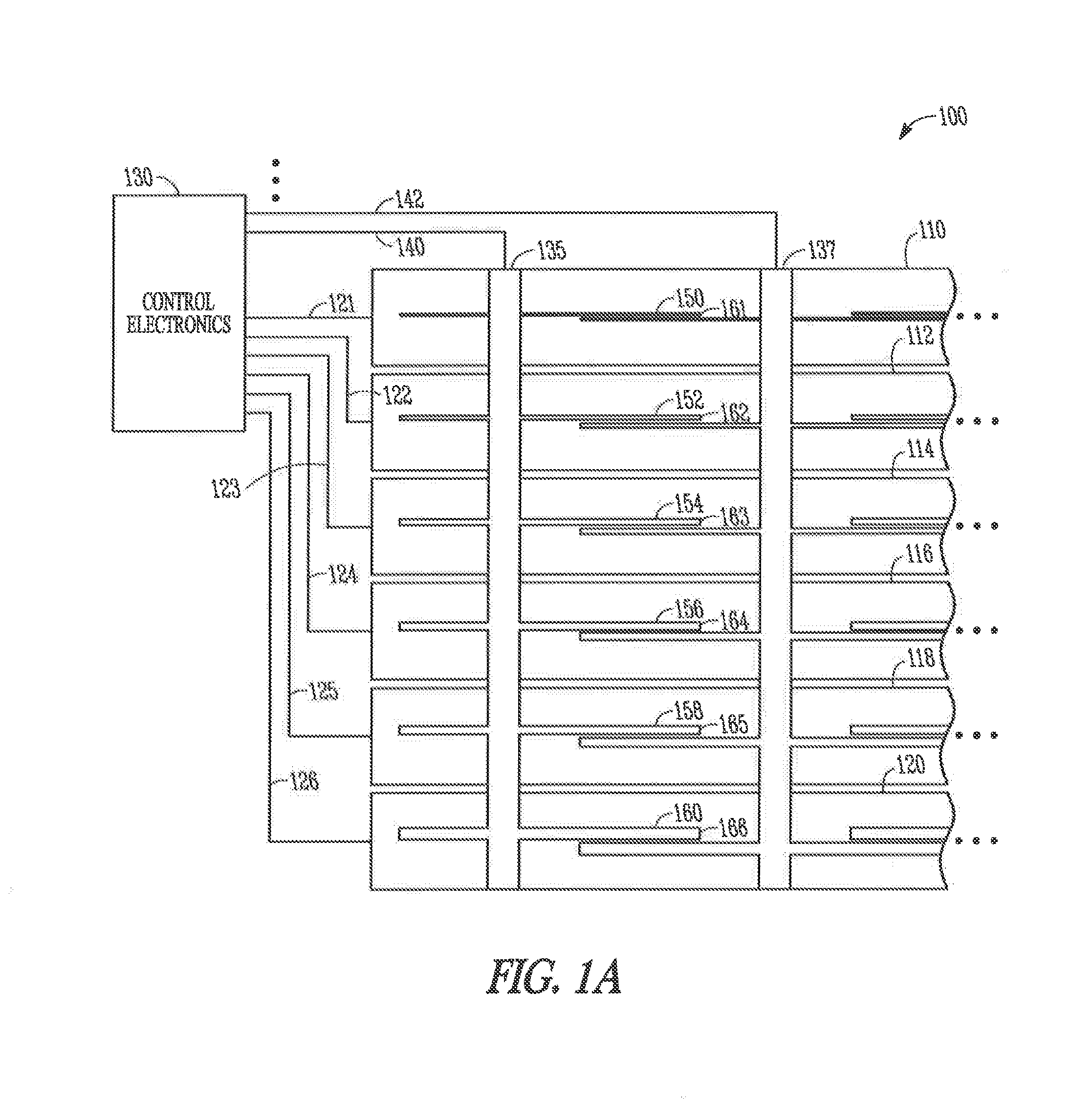
FIG. 1A is a schematic representation of an electrode layout for a touch sensitive device according to an example embodiment.
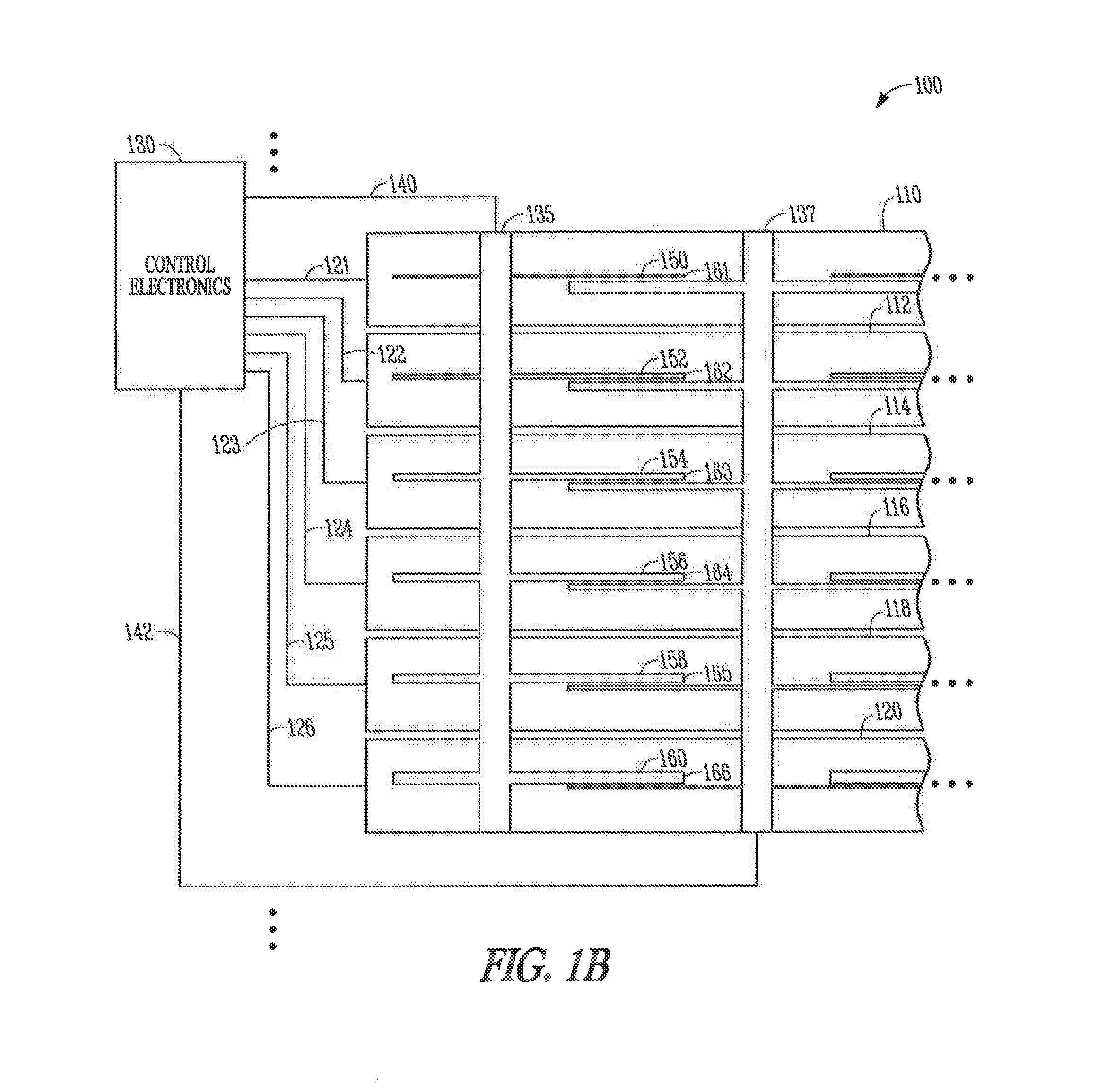
FIG. 1B is a schematic representation of an alternative electrode layout for a touch sensitive device according to an example embodiment.
FIG. 2 is a schematic representation of an alternative sense electrode layout according to an example embodiment.
FIG. 3 is a schematic representation of a further alternative sense electrode layout according to an example embodiment.
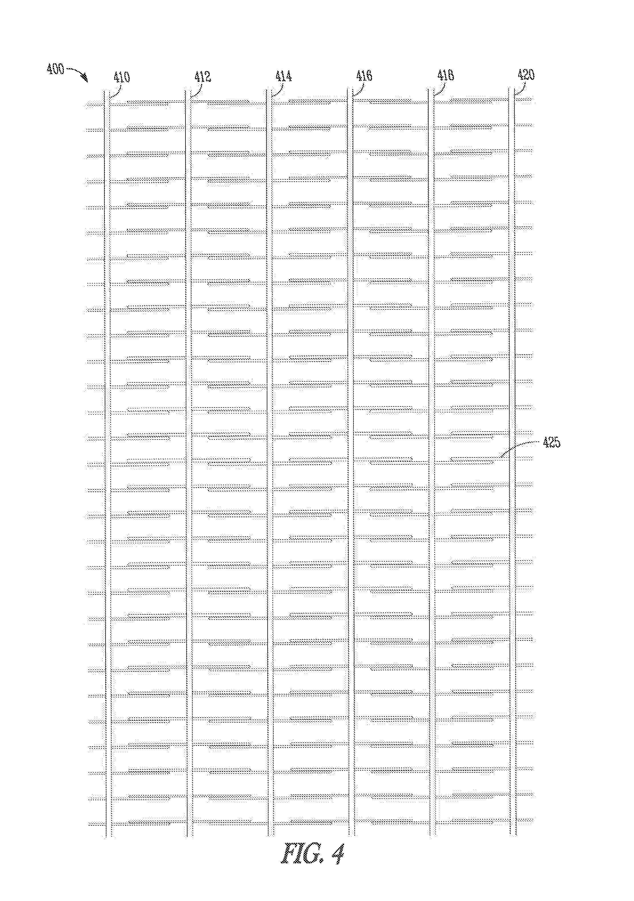
FIG. 4 is a schematic representation of a further alternative sense electrode layout for a touch sensitive device according to an example embodiment.
DETAILED DESCRIPTION
FIGS. 1A and 1B are schematic representations of an electrode layout for an example touch sensitive device 100 such as a touchscreen. In one embodiment, a plurality of longitudinal drive electrodes 110, 112, 114, 116, 118, and 120 are formed in one layer. The drive electrodes may also be referred to as X electrodes. In the example shown, the drive electrodes are bar shaped, and completely filled in to help create a shield from electric field interference from an underlying display device, such as a liquid crystal display (LCD). This type of drive electrode layout may be referred to as a flooded X pattern. The distance between the drive electrodes may be minimized in one embodiment to provide better shielding. The dimensions shown in the drawings may not be to scale and are not meant to be an accurate representation of the dimensions that may be used in various embodiments, but rather may be exaggerated to more clearly illustrate the concepts described herein.
In further embodiments, the drive electrodes 110, 112, 114, 116, 118, and 120 may be other than rectangular in shape, and may have more of a zig-zag pattern to minimize their visibility.
The drive electrodes 110, 112, 114, 116, 118, and 120 may be coupled via drive lines 121, 122, 123, 124, 125, and 126 to electronics 130 to drive the drive electrodes during operation of the touch sensitive device 100. In addition to the drive electrodes, one or more sense electrodes 135, 137 may run transverse to the drive electrodes. In one embodiment, the sense electrodes 135, 137 may be formed of a conductive transparent material such as indium tin oxide (ITO) or transparent conductive polymers. Such materials, which while conductive, have a resistance. The resistance of electrodes made of such materials may change depending on the width of the electrode.
The sense electrodes 135, 137 may be coupled to electronics 130 via connection lines 140 and 142 respectively. In one embodiment, the connection lines 140 and 142 may be highly conductive and formed of metal. The sense electrodes are single connected in one embodiment, in that only one end of the sense electrodes is coupled to the electronics 130. In one embodiment, sense electrodes 135 and 137 include a spine that runs transverse to the drive electrodes, and may also include crossbars transverse to the spine of sense electrode 135 and having different widths as indicated at 150, 152, 154, 156, 158, and 160. The crossbars run in the same direction as corresponding drive electrodes and are positioned over the respective drive electrodes 110, 112, 114, 116, 118, and 120.
In one embodiment, the crossbars extend from both sides of the spines, and have tips indicated on one end of the crossbars at 161, 162, 163, 164, 165, and 166 that are the furthest distance from the spine 135. The other ends of the crossbars may be the same distance from the spine 135 in various embodiments. The width of the crossbars in one embodiment increases with distance from the end of the spines coupled to the connection lines 140, 142. The increase in width decreases the resistance of the crossbars while increasing their capacitance to the drive electrodes. In one embodiment, the increase in width keeps the charge transfer time of each crossbar at or under a desired threshold. The charge transfer time is the time it takes to transfer sufficient charge from the drive electrodes through the sense electrodes to the sense capacitor. In a further embodiment, the charge transfer time of each crossbar is substantially equal, taking into account process tolerances.
Thus, it can be observed that the width of crossbar 150 is fairly narrow. The width increases with successive crossbars 152-160 such that the widest crossbar 160 is furthest from the connection line 140. In one example embodiment, the width of the spine of sense electrode 135 may be approximately 1 mm, and the width of the crossbars may progress from 0.2 mm to 0.5 mm or wider, including wider than the spine in some embodiments. Note that spine 137 has corresponding crossbars, as would additional spines as represented by the dots. The crossbars from adjacent spines may run adjacent to each other in further embodiments. In one embodiment, the crossbars extend about 75 percent of the distance between the spines, and thus run adjacent together for about 50 percent of their length as shown. The amount of adjacent run may vary in further embodiments. The spines may be narrower or wider than 1 mm in various embodiments consistent with desired charge transfer time and visibility constraints.
In one embodiment, the widths of the crossbars may be determined by starting with the worst case charge transfer time. In FIGS. 1A and 1B, the worst case charge transfer time would be the longest path from tip 166 of crossbar 160, along the spine of sense electrode 135 to connection line 140. After determining the width of crossbar 160 in accordance with a desired charge transfer time, the remaining crossbar widths are chosen to obtain charge transfer times equal to or less than the desired charge transfer time. The charge transfer time is generally a function of a resistance and a capacitance, where the resistance is the resistance from crossbar tip to the connection line of the sense electrode, and the capacitance is the capacitance between the drive electrodes and the sense electrode. The capacitance is affected by touch proximate the intersection of a sense electrode and a drive electrode. The worst case charge transfer time, T, may be calculated and used as a threshold or design parameter for ensuring that the charge transfer time at the tips of each crossbar is less than the worst case T, or equal to it. This results in the illustrated pattern of crossbar widths increasing with increased distance from the connection line.
Since some crossbars may be narrower, the capacitance may be reduced over the length of the sense electrodes. Sense electrodes may be increased in width to reduce the worst case charge transfer time. The use of wider crossbars for selected crossbars allows a reduction in the worst case charge transfer time. Narrower crossbars for selected crossbars reduces the capacitive coupling between the sense electrodes and the drive electrodes and hence allows a reduction in overall thickness of sensing portions of touch sensitive devices. This reduction in sense electrode layer thickness may result in a reduced overall touch sensitive device thickness, and may further reduce drive electrode to sense electrode separation.
In some embodiments, the worst case charge transfer time may be reduced by making some of the crossbars wider, while others already having a shorter charge transfer time may be made narrower.
In one embodiment, a sense electrode design may be optimized by making a worst case charge transfer time equal at all extremes of the electrode design. Such designs may or may not include crossbars, and the extremes of the design may or may not have electrode structures with equal widths. The charge transfer times of such sense electrodes should be substantially equal such that the charge transfer time does not adversely impact operation of a touch sensitive device. In one embodiment, the extremes of the design may correspond to portions of the electrode design that are furthest from a connection line that has a relatively higher conductivity than that of the electrode. In further embodiments, the extremes of the electrode design may additionally correspond to portions of the electrode design that have smaller widths than other portions of the design, and may not directly correspond to portions of the design that are furthest from higher conductivity connection lines. In some embodiments, there may be a mixture of such extremes, including remote portions and narrow portions of the electrodes. In one embodiment, the width of such portions may be modified to ensure that the sense electrodes have a charge transfer time that is equal to or better than a desired worst case charge transfer time.
The layout of FIG. 1B shows sense electrodes with varying crossbar widths as described above. In FIG. 1B, adjacent sense electrodes are arranged to be coupled to connection lines on alternate opposite ends. This results in the width of electrodes progressing along the spines from alternate opposite ends. The adjacent crossbars from adjacent spines are arranged such that the widest crossbars runs adjacent to the narrowest crossbars, while crossbars of medium width run adjacent to each other. Thus the combined width of the adjacent crossbars may be fairly equal in some embodiments over the length of the spines.
FIG. 2 is a schematic representation of an alternative sense electrode layout 200 according to an example embodiment. Layout 200 shows one sense electrode 210 having a spine 215 with multiple transverse crossbars 220, 221, 222, 223, 224, 225, and 226. Sense electrode 210 in one embodiment is double connected, meaning that both ends of the sense electrode 210 are coupled to connection lines as indicated by connection lines 230 and 235. For each electrode, the corresponding connection lines 230 and 235 are coupled together for coupling to a controller to individually sense signals from the electrodes. Since sense electrode 210 is connected on both ends, the crossbar being furthest from a connection line is actually the middle crossbar 223. Crossbar 223 would be the crossbar exhibiting the worst case charge transfer time, but as shown, it has been widened to obtain a desired charge transfer time. The crossbars continue to decrease in width in both directions from crossbar 223 toward respective connection lines 230 and 235.
In one embodiment, with an odd number of crossbars, crossbars 222 and 224 may be equal in width, crossbars 221 and 225 may be equal in width, and crossbars 220 and 226 may also be equal in width. With an even number of crossbars, there may be two middle crossbars with equal width, rather than one. Both may be the same distance from a connection line, and thus, the worst case charge transfer time from their tips to the connection lines may be the same. The rest of the crossbars may be successively narrower, as there is no need to make them as wide as the widest crossbar. In fact, in one embodiment, it is desired that the charge transfer time from the tip of each crossbar to the nearest connection line be equal, meaning that the width is decreased as the distance to the nearest connection line decreases. Additional sense electrodes that have the varying width crossbar arrangement may be provided as indicated by the additional sense electrode with crossbars running adjacent crossbars 220, 221, 222, 223, 224, 225, and 226, and dots indicating a repeating pattern of sense electrodes. It is understood that the dimensions of FIG. 2, as well as the other drawings, may not be to scale and are not meant to be an accurate representation of the dimensions that may be used in various embodiments, but rather, the dimensions may be exaggerated to more clearly illustrate the concepts described herein.
FIG. 3 is a schematic representation of a further alternative sense electrode layout 300 according to an example embodiment. Layout 300 includes a sense electrode 310 having different widths 312, 314, 316, and 318 along its spine. Several transverse crossbars 320, 322, 324, and 326 are shown coupled to the sense electrode 310. As shown, the width of the spine increases with increasing distance from a single connected connection line 330. With each increase of spine width in one embodiment, a crossbar is coupled to the sense electrode. The crossbars may be connected at other points on the sense electrode where the sense electrode does not transition in width. In further embodiments, the width of the sense electrode may continuously vary, or may vary in a stepwise manner, with multiple crossbars coupled to each section of constant width. Various embodiments may include adjacent sense electrodes arranged to be coupled to connection lines on alternate opposite ends as illustrated in FIG. 1B.
The crossbars 320, 322, 324 and 326 are also shown as varying in their width. As previously described, the worst case charge transfer time from a tip of the crossbar farthest from the connection line 330 may be used. In this case, that would be crossbar 326. The charge transfer time again is the total charge transfer time from the tip of the crossbar 326 to the connection line 330. In this case, the charge transfer time may be reduced by the fact that the spine is increasing in width. Thus, the width of crossbar 326 may not be as wide as in previous embodiments to meet a desired worst case charge transfer time. The same reduction in width for succeeding crossbars closer to connection line 330 may also be obtained. As with previous electrode patterns, additional spines with crossbars may be provided in various patterns to obtain a pattern having a desired area.
FIG. 4 is a schematic representation of a further alternative sense electrode layout 400 for a touch screen. Six spines 410, 412, 414, 416, 418 and 420 are shown and representative of sense electrodes for an entire touchscreen in one embodiment. Each of the spines may be double connected such that both ends may be coupled to sense circuitry. Similar to FIG. 2, each spine has multiple transverse crossbars. Twenty nine crossbars per spine are illustrated. Since the spines are connected on both ends, the crossbar being furthest from a low resistance connection (not shown) to the sense circuitry is actually the middle crossbar 425, which is the 15th crossbar from either end of the spines. Crossbar 425 is thus the crossbar exhibiting the worst case charge transfer time until it is widened as shown to obtain a desired charge transfer time. The crossbars continue to decrease in width in both directions from crossbar 425 toward respective connections to sense circuitry.
* * * * *
D00000
D00001
D00002
D00003
D00004
D00005
XML
uspto.report is an independent third-party trademark research tool that is not affiliated, endorsed, or sponsored by the United States Patent and Trademark Office (USPTO) or any other governmental organization. The information provided by uspto.report is based on publicly available data at the time of writing and is intended for informational purposes only.
While we strive to provide accurate and up-to-date information, we do not guarantee the accuracy, completeness, reliability, or suitability of the information displayed on this site. The use of this site is at your own risk. Any reliance you place on such information is therefore strictly at your own risk.
All official trademark data, including owner information, should be verified by visiting the official USPTO website at www.uspto.gov. This site is not intended to replace professional legal advice and should not be used as a substitute for consulting with a legal professional who is knowledgeable about trademark law.