Compound semiconductor film structure
Yang
U.S. patent number 10,229,976 [Application Number 15/262,306] was granted by the patent office on 2019-03-12 for compound semiconductor film structure. This patent grant is currently assigned to LEXTAR ELECTRONICS CORPORATION. The grantee listed for this patent is Lextar Electronics Corporation. Invention is credited to Chung-Chieh Yang.


| United States Patent | 10,229,976 |
| Yang | March 12, 2019 |
Compound semiconductor film structure
Abstract
A compound semiconductor film structure includes a substrate, a first compound semiconductor epitaxial layer and a second compound semiconductor epitaxial layer. The substrate has a top surface. The first compound semiconductor epitaxial layer is formed on the top surface and has an epitaxial interface and at least one recess, wherein the epitaxial interface is disposed on one side of the first compound semiconductor epitaxial layer opposite to the side of the first compound semiconductor epitaxial layer facing the top surface, and the at least one recess is formed in the first compound semiconductor epitaxial layer. The second compound semiconductor epitaxial layer formed on the epitaxial interface. The top surface and the bottom of recess are separated by a distance substantially ranging between 0.8 .mu.m and 1.3 .mu.m.
| Inventors: | Yang; Chung-Chieh (Taiching, TW) | ||||||||||
|---|---|---|---|---|---|---|---|---|---|---|---|
| Applicant: |
|
||||||||||
| Assignee: | LEXTAR ELECTRONICS CORPORATION
(Hsinchu, TW) |
||||||||||
| Family ID: | 57189850 | ||||||||||
| Appl. No.: | 15/262,306 | ||||||||||
| Filed: | September 12, 2016 |
Prior Publication Data
| Document Identifier | Publication Date | |
|---|---|---|
| US 20170117368 A1 | Apr 27, 2017 | |
Foreign Application Priority Data
| Oct 22, 2015 [TW] | 104134646 A | |||
| Current U.S. Class: | 1/1 |
| Current CPC Class: | H01L 21/0243 (20130101); H01L 21/02494 (20130101); H01L 29/0692 (20130101); H01L 21/02502 (20130101); H01L 29/2003 (20130101); H01L 21/02647 (20130101); H01L 21/30612 (20130101); H01L 21/02458 (20130101); H01L 29/205 (20130101); H01L 21/0254 (20130101); H01L 21/0242 (20130101); H01L 21/0265 (20130101) |
| Current International Class: | H01L 29/20 (20060101); H01L 21/306 (20060101); H01L 21/02 (20060101); H01L 29/06 (20060101); H01L 29/205 (20060101) |
References Cited [Referenced By]
U.S. Patent Documents
| 7491984 | February 2009 | Koike et al. |
| 8659031 | February 2014 | Kim |
| 9034739 | May 2015 | Wang |
| 2010/0099213 | April 2010 | Wu et al. |
| 2011/0204378 | August 2011 | Su |
| 2012/0258286 | October 2012 | Amano |
| 2014/0264415 | September 2014 | Okuno |
| 2015/0280058 | October 2015 | Kappers et al. |
| 2488587 | Sep 2012 | GB | |||
| 2002293698 | Oct 2002 | JP | |||
| 2011-134948 | Jul 2011 | JP | |||
| 2001-345281 | Dec 2011 | JP | |||
| 2014-509781 | Apr 2014 | JP | |||
| 201203322 | Jan 2012 | TW | |||
Other References
|
TW Office Action dated May 12, 2016 in corresponding Taiwan application (No. 104134646). cited by applicant . Hirayama, et al.: "Milliwatt power 270 nm-band AlGaN deep-UV LEDs fabricated on ELO-AIN templates"; hys. Status Solidi C 6, No. S2, S474-S477 (2009) / DOI 10.1002/pssc.200880959; pp. 1-4. cited by applicant . EP Search Report dated Feb. 24, 2017 in European application (No. 16194832.8-1552). cited by applicant . JPO Office Action dated Mar. 6, 2018 in JP application (No. 2016196308). cited by applicant . Japanese language office action dated Sep. 29, 2017, issued in application No. JP 2016-196308, and its English language translation. cited by applicant. |
Primary Examiner: Hossain; Moazzam
Assistant Examiner: Isaac; Stanetta D
Attorney, Agent or Firm: McClure, Qualey & Rodack, LLP
Claims
What is claimed is:
1. A compound semiconductor film structure, comprising: a substrate having a top surface without patterned holes or protrusions; a first compound semiconductor epitaxial layer formed on the top surface, wherein an epitaxial interface is disposed one side of the first compound semiconductor epitaxial layer opposite to one side of the first compound semiconductor epitaxial layer facing the top surface, and at least one recess is formed in the first compound semiconductor epitaxial layer; and a second compound semiconductor epitaxial layer formed on the epitaxial interface to cover the at least one recess but not completely fill up the at least one recess; wherein the top surface and a bottom of the recess are separated by a distance substantially ranging between 0.8 and 1.3 micrometers (.mu.m).
2. The compound semiconductor film structure according to claim 1, wherein the recess has a cross-sectional profile which is wider at the top but narrower at the bottom.
3. The compound semiconductor film structure according to claim 1, wherein the first compound semiconductor epitaxial layer further has a plurality of irregularly arranged recesses.
4. The compound semiconductor film structure according to claim 1, wherein the first compound semiconductor epitaxial layer and the second compound semiconductor epitaxial layer both comprise an aluminum containing semiconductor material.
5. The compound semiconductor film structure according to claim 4, wherein the aluminum containing semiconductor material is selected from a group consisting of aluminum nitride (AlN), aluminum gallium nitride (AlGaN), aluminum indium gallium nitride (AlInGaN) and arbitrary combinations thereof.
6. The compound semiconductor film structure according to claim 1, wherein the substrate is an AlN precursor layer disposed on a base board.
7. The compound semiconductor film structure according to claim 1, wherein the first compound semiconductor epitaxial layer has a thickness substantially ranging between 1 .mu.m and 1.5 .mu.m.
8. The compound semiconductor film structure according to claim 1, wherein the first compound semiconductor epitaxial layer has a honeycomb shaped profile in a plan view.
9. The compound semiconductor film structure according to claim 1, wherein the first compound semiconductor epitaxial layer has a plurality of irregularly arranged island structures, and each of the island structures has a diameter substantially ranging between 2 .mu.m and 4 .mu.m.
10. The compound semiconductor film structure according to claim 1, wherein the recess has an opening width substantially ranging between 0.1 .mu.m and 0.5 .mu.m.
11. A compound semiconductor film structure, comprising: a substrate having a top surface; a first compound semiconductor epitaxial layer formed on the top surface, wherein an epitaxial interface is disposed one side of the first compound semiconductor epitaxial layer opposite to one side of the first compound semiconductor epitaxial layer facing the top surface, and at least one recess is formed in the first compound semiconductor epitaxial layer; and a second compound semiconductor epitaxial layer formed on the epitaxial interface to cover the at least one recess but not completely fill up the at least one recess; wherein the top surface and a bottom of the recess are separated by a distance substantially ranging between 0.8 and 1.3 micrometers (.mu.m); the first compound semiconductor epitaxial layer and the second compound semiconductor epitaxial layer are formed in situ.
Description
This application claims the benefit of Taiwan application Serial No. 104134646, filed Oct. 22, 2015, the disclosure of which is incorporated by reference herein in its entirety.
TECHNICAL FIELD
The disclosure relates in general to a semiconductor film structure, and more particularly to a compound semiconductor film structure.
BACKGROUND
The III-V nitride-based compound semiconductor composed of 3B elements containing aluminum (Al), gallium (Ga) or indium (In) and 5B elements containing nitrogen (N) has a wide energy gap and can be used for manufacturing electronic components such as semiconductor laser diodes (LD), light emitting diodes (LED), detectors, and high frequency and high power transistors.
Currently, other than sapphire substrates and silicon substrates, a substrate more suitable for epitaxy growth of the III-V nitride-based compound semiconductor layer is still not available, a large lattice mismatch may occur between the III-V nitride-based compound semiconductor layer and the sapphire substrate or the silicon substrate, and this may cause dislocation to the epitaxial layer and deteriorate the performance of device using the semiconductor film structure. To improve the quality of the semiconductor film structure and decrease dislocation density there between, various technologies for improving the quality of epitaxial growth, such as low temperature buffer layer technology, layer insertion technology, and epitaxial laterally overgrowth (ELO) technology, are provided.
The conventional low temperature buffer layer technology and layer insertion technology both are characterized by the following steps. Firstly, a low temperature epitaxy growth is performed to form a low temperature buffer layer which is subsequently annealed at a high temperature, such that the low temperature buffer layer can have a lower nucleation density. Then, a second stage of high temperature epitaxy growth is performed on the annealed buffer layer. Although the nucleation density of the epitaxial layer can be largely reduced by these approaches, the epitaxial structure of the epitaxial layer still has a large dislocation density. As for the ELO technology, regular holes or protrusions should be firstly formed on the epitaxial growth surface using by etching process in order to block the lattice defects extending upwards during the subsequent epitaxy growth process. Relatively complicated manufacturing process is required. Furthermore, the critical dimension and the process window of the mask used in the ELO technology are micrometer scaled. Besides the ELO technology requires longer manufacturing time and higher manufacturing cost. Therefore the applying the ELO technology to form an epitaxial structure with a large area can be rather costly.
Therefore, it has become a prominent task to provide an advanced compound semiconductor film structure to resolve the problems encountered in prior art.
SUMMARY
According to one embodiment, a compound semiconductor film structure is provided. The compound semiconductor film structure includes a substrate, a first compound semiconductor epitaxial layer and a second compound semiconductor epitaxial layer. The substrate has a top surface. The first compound semiconductor epitaxial layer is formed on the top surface and has an epitaxial interface and at least one recess, wherein the epitaxial interface is disposed on one side of the first compound semiconductor epitaxial layer opposite to the side of the first compound semiconductor epitaxial layer facing the top surface, and the at least one recess is formed in the first compound semiconductor epitaxial layer. The second compound semiconductor epitaxial layer formed on the epitaxial interface. The top surface and the bottom of recess are separated by a distance substantially ranging between 0.8 micrometers (.mu.m) and 1.3 .mu.m.
According to the above embodiment of the present disclosure, a compound semiconductor film structure is provided. A first compound semiconductor film whose thickness substantially ranges between 1 .mu.m and 1.5 .mu.m is formed on a top surface of a substrate by an epitaxial growth technology, wherein the compound semiconductor film has a plurality of regularly arranged island structures separated by a plurality of recesses. Then, a second compound semiconductor film is formed on the island structures and covers the recess to form a compound semiconductor film structure having a plurality of irregularly arranged gaps (recesses), wherein the top surface of the substrate and the bottom of the recesses are separated by a distance substantially ranging between 0.8 .mu.m and 1.3 .mu.m.
Because the gaps (recesses) can block the lattice defects extending upwards in the epitaxy process, the dislocation density of the second compound semiconductor epitaxial layer thus can be reduced and the quality of the compound semiconductor film structure can be improved. In addition, a self-assembled compound semiconductor film structure can be formed on the substrate by merely using an epitaxial growth process, additional etching process used to form regular holes or protrusions on the substrate required by the ELO technology can be omitted, the process for fabricating the compound semiconductor film structure can be simplified and the manufacturing cost can be reduced accordingly.
The above and other aspects of the present disclosure will become better understood with regard to the following detailed description of the preferred but non-limiting embodiment(s). The following description is made with reference to the accompanying drawings.
BRIEF DESCRIPTION OF THE DRAWINGS
FIGS. 1A to 1C are cross-sectional views illustrating the process structures for forming a compound semiconductor film structure according to an embodiment of the present disclosure;
FIG. 2 is an electron microscopy image of the first compound semiconductor epitaxial layer as depicted in FIG. 1B, wherein the image is captured using a scanning electron microscope (SEM); and
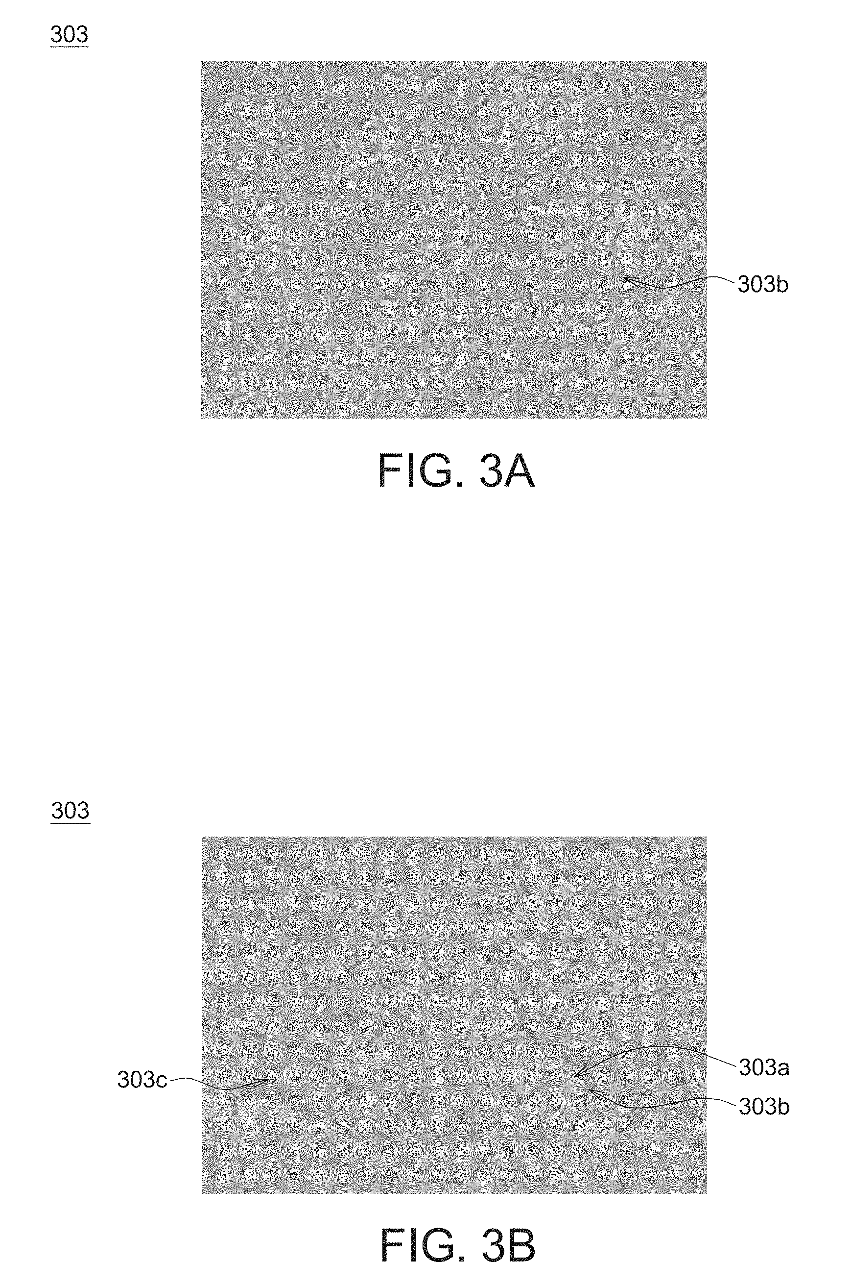
FIGS. 3A and 3B are electron microscopy images of a first compound semiconductor epitaxial layer respectively taken at the time while the growth thickness is substantially smaller than 1 .mu.m and greater than 1.5 .mu.m, wherein the images are captured using an SEM.
DETAILED DESCRIPTION
The disclosure provides a compound semiconductor film structure capable of resolving the problems resulted from high dislocation density and lattice defects of the conventional III-V nitride-based compound semiconductor epitaxy film and at the same time simplifying the manufacturing process and reducing the manufacturing cost. For the object, technical features and advantages of the present invention to be more easily understood by anyone ordinary skilled in the technology field, a number of exemplary embodiments based on the compound semiconductor film structure and the manufacturing method thereof are disclosed below with detailed descriptions and accompanying drawings.
It should be noted that these embodiments are for exemplification purpose only, not for limiting the scope of protection of the invention. The invention can be implemented by using other features, elements, methods and parameters. The preferred embodiments are merely for illustrating the technical features of the invention, not for limiting the scope of protection of. Anyone skilled in the technology field of the invention will be able to make suitable modifications or changes based on the specification disclosed below without breaching the spirit of the invention. Designations common to the accompanying drawings are used to indicate identical or similar elements.
FIGS. 1A to 1C are sectional views illustrating the process structures for forming a compound semiconductor film structure 100 according to an embodiment of the present disclosure. The method for manufacturing the compound semiconductor film structure 100 includes following steps: Firstly, a substrate 101 is provided (as indicated in FIG. 1A). In some embodiments of the present disclosure, the substrate 101 can be realized by a sapphire substrate, a semiconductor substrate, a ceramic substrate or a plastic substrate. In some other embodiments of the present disclosure, the substrate 101 can be realized by a semiconductor precursor layer 101b disposed on a base board, such as a sapphire substrate, a semiconductor the substrate, a ceramic substrate or a plastic substrate. In the present embodiment, the substrate 101 can be realized by an aluminum nitride (AlN) precursor layer 101b disposed on the sapphire substrate 101a.
Then, a first epitaxial growth process 102 is performed on the top surface 101c of the substrate 101 (the AlN precursor layer 101b) to form a first compound semiconductor epitaxial layer 103 (as indicated in FIG. 1B).
In some embodiments of the present disclosure, the first compound semiconductor epitaxial layer 103 includes an aluminum containing semiconductor material selected from a group consisting of aluminum nitride (AlN), aluminum gallium nitride (AlGaN), aluminum indium gallium nitride (AlInGaN) and the arbitrary combinations thereof. In the present embodiment, the first compound semiconductor epitaxial layer 103 preferably is realized by an AlN epitaxial layer.
Referring to FIG. 2, FIG. 2 is an electron microscopy image of the first compound semiconductor epitaxial layer 103 as depicted in FIG. 1B, wherein the image is captured using an SEM. The AlN epitaxial layer (the first compound semiconductor epitaxial layer 103) formed by the first epitaxial growth process 102 has a plurality of regularly arranged hexagonal island structures 103a. Each island structure 103a has a diameter R substantially ranging between 2 .mu.m and 4 .mu.m. As indicated in FIG. 2, the first compound semiconductor epitaxial layer 103 has a honeycomb shaped profile taken from the top view of the electron microscopy image.
In details, the first compound semiconductor epitaxial layer 103 has a plurality of recesses 103b used to divide the first compound semiconductor epitaxial layer 103 into a plurality of regularly arranged hexagonal island structures 103a. Each recess 103b has a cross-sectional profile wider at the top but narrower at the bottom and an opening width W1 substantially ranging between 0.1 .mu.m and 0.5 .mu.m. The recesses 103b can be put together to form a pattern and the first compound semiconductor epitaxial layer 103 can be divided into a plurality of regularly arranged hexagonal conical island structures 103a by the pattern (as indicated in FIG. 1B).
Furthermore, each island structure 103a of the first compound semiconductor epitaxial layer 103 has a substantially flat top 103c. In the present embodiment, the top 103c of each island structure 103a is a surface substantially parallel to a c-plane of the AlN epitaxial layer. It should be noted that, the context that each island structure 103a of the first compound semiconductor epitaxial layer 103 has a substantially flat top 103c only when the thickness H of the first compound semiconductor epitaxial layer 103 is satisfied certain conditions. In some embodiments of the present disclosure, the thickness H of the first compound semiconductor epitaxial layer 103 must be restricted within the range between 1 .mu.m and 1.5 .mu.m. If the thickness H of the first compound semiconductor epitaxial layer 103 is too large or too small, each island structure 103a cannot have a substantially flat top 103c.
Referring to FIG. 3A and FIG. 3B, FIG. 3A and FIG. 3B are electron microscopy images of a first compound semiconductor epitaxial layer 303 respectively taken at the time while the growth thickness is substantially smaller than 1 .mu.m and greater than 1.5 .mu.m, wherein the images are captured using an SEM. As indicated in FIG. 3A, when the growth thickness of the first compound semiconductor epitaxial layer 303 is substantially smaller than 1 .mu.m, the recess 303b formed in the first compound semiconductor epitaxial layer 303 are still irregular cracks that cannot put together to form a pattern to divide the first compound semiconductor epitaxial layer 303 into a plurality of regularly arranged hexagonal conical island structures (as indicated in FIG. 2).
As indicated in FIG. 3B, when the growth thickness of the first compound semiconductor epitaxial layer 303 is substantially greater than 1.5 .mu.m, it can be determined that the top 303c of the hexagonal conical island structure 303a of the first compound semiconductor epitaxial layer 303 has irregularly distributed shadows. In other words, each top 303c of the hexagonal conical island structures 303a is no more a flat surface parallel to the same lattice direction of the AlN epitaxial layer; and the fact can be proved by the measurement of the X-ray reflectance of the top 303c of the hexagonal conical island structures 303a.
Then, a second epitaxial growth process 104 is performed to form a second compound semiconductor epitaxial layer 105 on the first compound semiconductor epitaxial layer 103, such that the compound semiconductor film structure 100 as shown in FIG. 1C can be formed. The second epitaxial growth process 104 continues with the first epitaxial growth process 102, but has a higher temperature for epitaxial growth. The thickness of the second epitaxial growth process 104 substantially ranges between 0.5 .mu.m and 1 .mu.m, and preferably is equivalent to 0.8 .mu.m.
During the second epitaxial growth process 104, the compound semiconductor material formed by epitaxy does not completely fill up the recess 103b, but is randomly inserted into the recess 103b formed in the first compound semiconductor epitaxial layer 103, whereby a plurality of irregularly arranged recesses 103b' (gaps) are gradually formed. The second compound semiconductor epitaxial layer 105 covers the recess 103b' and directly contacts the top 103c of the hexagonal conical island structure 103a of the first compound semiconductor epitaxial layer 103, and an epitaxial interface 106 is formed between the second compound semiconductor epitaxial layer 105 and the first compound semiconductor epitaxial layer 103. In details, the epitaxial interface 106 is disposed on one side of the first compound semiconductor epitaxial layer 103 opposite to the side of the first compound semiconductor epitaxial layer facing the top surface 101c of the substrate 101. Besides, the top surface 101c of the substrate 101 and the bottom of the recess 103b' are separated by a distance D substantially ranging between 0.8 .mu.m and 1.3 .mu.m.
In the present embodiment, the top 103c of each island structure 103a of the first compound semiconductor epitaxial layer 103 has a surface substantially parallel to a c-plane direction of the AlN epitaxial layer and can provide a substantially flat surface allowing the second epitaxial growth process 104a performed thereon. Furthermore, the recess 103b' can block the lattice defects extending upwards in the epitaxy growth process, and therefore reduce the dislocation density of the second compound semiconductor epitaxial layer 105 and increase the quality of the compound semiconductor film structure 100.
In some embodiments of the present disclosure, the first epitaxial growth process 102 and the second epitaxial growth process 104 can be performed in the same reaction chamber to form a self-assembled compound semiconductor film structure 100 in situ, additional etching process used to form regular holes or protrusions on the substrate required by the ELO technology is no more necessary, such that the objects of simplifying the manufacturing process and reducing the manufacturing cost can be achieved.
According to the above embodiment of the present disclosure, a compound semiconductor film structure is provided. A first compound semiconductor film whose thickness substantially ranges between 1 .mu.m and 1.5 .mu.m is formed on a top surface of a substrate by an epitaxial growth technology, wherein the compound semiconductor film has a plurality of regularly arranged island structures separated by a plurality of recesses. Then, a second compound semiconductor film is formed on the island structures and covers the recess to form a compound semiconductor film structure having a plurality of irregularly arranged gaps (recesses), wherein the top surface of the substrate and the bottom of the recesses are separated by a distance substantially ranging between 0.8 .mu.m and 1.3 .mu.m.
Because the gaps (recesses) can block the lattice defects extending upwards in the epitaxy process, the dislocation density of the second compound semiconductor epitaxial layer thus can be reduced and the quality of the compound semiconductor film structure can be improved. In addition, a self-assembled compound semiconductor film structure can be formed on the substrate by merely using an epitaxial growth process, additional etching process used to form regular holes or protrusions on the substrate required by the ELO technology can be omitted, the process for fabricating the compound semiconductor film structure can be simplified and the manufacturing cost can be reduced accordingly.
It will be apparent to those skilled in the art that various modifications and variations can be made to the disclosed embodiments. It is intended that the specification and examples be considered as exemplary only, with a true scope of the disclosure being indicated by the following claims and their equivalents.
* * * * *
D00000
D00001
D00002
D00003
XML
uspto.report is an independent third-party trademark research tool that is not affiliated, endorsed, or sponsored by the United States Patent and Trademark Office (USPTO) or any other governmental organization. The information provided by uspto.report is based on publicly available data at the time of writing and is intended for informational purposes only.
While we strive to provide accurate and up-to-date information, we do not guarantee the accuracy, completeness, reliability, or suitability of the information displayed on this site. The use of this site is at your own risk. Any reliance you place on such information is therefore strictly at your own risk.
All official trademark data, including owner information, should be verified by visiting the official USPTO website at www.uspto.gov. This site is not intended to replace professional legal advice and should not be used as a substitute for consulting with a legal professional who is knowledgeable about trademark law.