Placement method for circuit carrier and circuit carrier
Karch Feb
U.S. patent number 10,217,675 [Application Number 14/836,049] was granted by the patent office on 2019-02-26 for placement method for circuit carrier and circuit carrier. This patent grant is currently assigned to A.B. MIKROELEKTRONIK GESELLSCHAFT MIT BESCHRAENKTER HAFTUNG. The grantee listed for this patent is A.B. Mikroelektronik Gesellschaft mit beschraenkter Haftung. Invention is credited to Andreas Karch.


| United States Patent | 10,217,675 |
| Karch | February 26, 2019 |
Placement method for circuit carrier and circuit carrier
Abstract
The invention concerns a process for the production of a circuit carrier (1) equipped with at least one surface-mount LED (SMD-LED), wherein the at least one SMD-LED (2) is positioned in oriented relationship to one or more reference points (3) of the circuit carrier (1) on the circuit carrier (1), wherein the position of a light-emitting region (4) of the at least one SMD-LED (2) is optically detected in the SMD-LED (2) and the at least one SMD-LED (2) is mounted to the circuit carrier (1) in dependence on the detected position of the light-emitting region (4) of the at least one SMD-LED (2), and such a circuit carrier (1).
| Inventors: | Karch; Andreas (Uebersee, DE) | ||||||||||
|---|---|---|---|---|---|---|---|---|---|---|---|
| Applicant: |
|
||||||||||
| Assignee: | A.B. MIKROELEKTRONIK GESELLSCHAFT
MIT BESCHRAENKTER HAFTUNG (Salzburg, AT) |
||||||||||
| Family ID: | 50239345 | ||||||||||
| Appl. No.: | 14/836,049 | ||||||||||
| Filed: | August 26, 2015 |
Prior Publication Data
| Document Identifier | Publication Date | |
|---|---|---|
| US 20150364384 A1 | Dec 17, 2015 | |
Related U.S. Patent Documents
| Application Number | Filing Date | Patent Number | Issue Date | ||
|---|---|---|---|---|---|
| PCT/AT2014/000027 | Feb 7, 2014 | ||||
Foreign Application Priority Data
| Feb 28, 2013 [AT] | A 155/2013 | |||
| Current U.S. Class: | 1/1 |
| Current CPC Class: | H05K 13/0812 (20180801); H01L 24/75 (20130101); H05K 13/046 (20130101); H05K 13/0815 (20180801); H01L 24/83 (20130101); H05K 1/0269 (20130101); H05K 3/303 (20130101); H01L 22/12 (20130101); H01L 33/62 (20130101); H01L 2224/293 (20130101); H01L 2224/83101 (20130101); H01L 2224/83862 (20130101); Y02P 70/50 (20151101); H01L 33/486 (20130101); H01L 2224/83192 (20130101); H05K 3/321 (20130101); H05K 2203/166 (20130101); H01L 24/29 (20130101); H01L 25/13 (20130101); Y02P 70/613 (20151101); H01L 2224/831 (20130101); H01L 2224/83122 (20130101); H01L 2224/83874 (20130101); H01L 2924/12041 (20130101); H01L 2224/83815 (20130101); H01L 24/32 (20130101); H01L 2224/2732 (20130101); H01L 24/27 (20130101); H01L 2224/83905 (20130101); H05K 2201/10106 (20130101); H01L 2224/32227 (20130101); H01L 2224/75745 (20130101); H01L 2224/29339 (20130101); H01L 2224/8384 (20130101); H01L 2224/83885 (20130101); H05K 3/341 (20130101); H01L 2224/29294 (20130101); H01L 2224/29339 (20130101); H01L 2924/00014 (20130101); H01L 2224/831 (20130101); H01L 2924/00012 (20130101); H01L 2224/83101 (20130101); H01L 2924/00012 (20130101); H01L 2224/2732 (20130101); H01L 2924/00014 (20130101); H01L 2224/83885 (20130101); H01L 2224/83874 (20130101); H01L 2224/83862 (20130101); H01L 2224/83862 (20130101); H01L 2224/83885 (20130101); H01L 2224/83874 (20130101); H01L 2224/83905 (20130101); H01L 2224/83815 (20130101); H01L 2224/83874 (20130101); H01L 2224/83905 (20130101); H01L 2224/83815 (20130101); H01L 2224/83862 (20130101); H01L 2224/83905 (20130101); H01L 2224/83815 (20130101); H01L 2224/83862 (20130101); H01L 2224/83874 (20130101); H01L 2224/83905 (20130101); H01L 2224/83815 (20130101); H01L 2224/83874 (20130101); H01L 2224/83862 (20130101); H01L 2224/29294 (20130101); H01L 2924/00014 (20130101); H01L 2224/293 (20130101); H01L 2924/014 (20130101) |
| Current International Class: | H01L 23/00 (20060101); H05K 13/04 (20060101); H05K 13/08 (20060101); H05K 3/30 (20060101); H05K 1/02 (20060101); H01L 21/66 (20060101); H01L 25/00 (20060101); H05K 3/34 (20060101); H05K 3/32 (20060101) |
| Field of Search: | ;438/4 |
References Cited [Referenced By]
U.S. Patent Documents
| 4208005 | June 1980 | Nate |
| 4615093 | October 1986 | Tews et al. |
| 4916805 | April 1990 | Ellrich |
| 4980971 | January 1991 | Bartschat et al. |
| 5173759 | December 1992 | Murano |
| 5290986 | March 1994 | Colon |
| 5559727 | September 1996 | Deley et al. |
| 5758942 | June 1998 | Fogal et al. |
| 5854087 | December 1998 | Kurata |
| 5857767 | January 1999 | Hochstein |
| 5893511 | April 1999 | Schwarzbauer |
| 5917200 | June 1999 | Kurata |
| 5943586 | August 1999 | Koizuma et al. |
| 6023104 | February 2000 | Koizuma et al. |
| 6040895 | March 2000 | Haas |
| 6208419 | March 2001 | Yamamoto |
| 6266891 | July 2001 | Yamamoto |
| 6285782 | September 2001 | Inoue et al. |
| 6312624 | November 2001 | Kropp |
| 6359694 | March 2002 | Stredele et al. |
| 6369884 | April 2002 | Yamamoto |
| 6480223 | November 2002 | Grasmueller |
| 6542238 | April 2003 | Tsuboi et al. |
| 6693293 | February 2004 | Oomori et al. |
| 6956879 | October 2005 | Tatsuta |
| 7084353 | August 2006 | Downes |
| 7638814 | December 2009 | Wall, Jr. et al. |
| 7660336 | February 2010 | Knotz |
| 8015696 | September 2011 | Fukunaga |
| 8860045 | October 2014 | Lin |
| 2002/0187571 | December 2002 | Collins, III |
| 2002/0196639 | December 2002 | Weidel |
| 2003/0159279 | August 2003 | Bachthaler et al. |
| 2003/0206650 | November 2003 | Gladnick |
| 2004/0033679 | February 2004 | Jacobson |
| 2004/0076739 | April 2004 | Yokono et al. |
| 2004/0179209 | September 2004 | Besch |
| 2004/0239952 | December 2004 | Mueller |
| 2005/0014311 | January 2005 | Hayasaka |
| 2005/0093146 | May 2005 | Sakano |
| 2005/0105301 | May 2005 | Takeda et al. |
| 2006/0187982 | August 2006 | Knotz |
| 2006/0209910 | September 2006 | Fukunaga |
| 2006/0211240 | September 2006 | Chi |
| 2006/0231952 | October 2006 | Kim |
| 2006/0244117 | November 2006 | Karnezos |
| 2007/0187818 | August 2007 | Lyne |
| 2008/0023711 | January 2008 | Tarsa |
| 2008/0137106 | June 2008 | Ono |
| 2008/0156398 | July 2008 | Yasuda et al. |
| 2008/0160183 | July 2008 | Ide et al. |
| 2008/0186725 | August 2008 | Schlager et al. |
| 2008/0284311 | November 2008 | Schug |
| 2008/0315214 | December 2008 | Wall, Jr. et al. |
| 2009/0021141 | January 2009 | Emoto |
| 2009/0056111 | March 2009 | Muren |
| 2009/0090002 | April 2009 | Motomuro |
| 2009/0189949 | July 2009 | Wu |
| 2009/0251918 | October 2009 | Engl et al. |
| 2009/0269704 | October 2009 | Hodono |
| 2009/0272971 | November 2009 | Lee |
| 2009/0291296 | November 2009 | McConnelee |
| 2009/0321750 | December 2009 | Namioka |
| 2010/0023929 | January 2010 | Jones et al. |
| 2010/0053929 | March 2010 | Bisberg |
| 2010/0132187 | June 2010 | Nishino et al. |
| 2010/0164367 | July 2010 | Shioi |
| 2010/0237767 | September 2010 | Emoto |
| 2010/0246936 | September 2010 | Ji et al. |
| 2010/0284198 | November 2010 | Willwohl et al. |
| 2011/0032722 | February 2011 | Ishida et al. |
| 2011/0049541 | March 2011 | Katsuno |
| 2011/0309384 | December 2011 | Ito et al. |
| 2012/0063157 | March 2012 | Nakazato et al. |
| 2012/0081618 | April 2012 | Matsui |
| 2012/0217531 | August 2012 | Katsuno |
| 2012/0230011 | September 2012 | Harada |
| 2012/0249779 | October 2012 | Ji et al. |
| 2012/0262567 | October 2012 | Tsuboi et al. |
| 2012/0313207 | December 2012 | Oganesian |
| 2012/0317802 | December 2012 | Yamamoto et al. |
| 2013/0063918 | March 2013 | Haba |
| 2013/0245988 | September 2013 | Lai |
| 2014/0169014 | June 2014 | Jungwirth et al. |
| 2015/0041974 | February 2015 | Kobayashi |
| 2015/0069435 | March 2015 | Chen |
| 2015/0255419 | September 2015 | Nishimoto |
| 2016/0040857 | February 2016 | Inoue |
| 2016/0155693 | June 2016 | Smith |
| 2016/0291233 | October 2016 | Trutna |
| 2017/0051884 | February 2017 | Raring |
| 1275307 | Nov 2000 | CN | |||
| 1819761 | Aug 2006 | CN | |||
| 1853320 | Oct 2006 | CN | |||
| 201629347 | Nov 2010 | CN | |||
| 103079392 | May 2013 | CN | |||
| 34 45 625 | Jun 1986 | DE | |||
| 38 27 151 | Jul 1989 | DE | |||
| 197 11 138 | Sep 1998 | DE | |||
| 101 28 476 | Jan 2003 | DE | |||
| 101 62 270 | Jul 2003 | DE | |||
| 10 2005 005 896 | Jan 2011 | DE | |||
| 10 2009 028 499 | Feb 2011 | DE | |||
| 10 2010 031 939 | Jan 2012 | DE | |||
| 10 2011 109 226 | Feb 2013 | DE | |||
| 0269337 | Jun 1988 | EP | |||
| 0 622 837 | Nov 1994 | EP | |||
| 0 781 660 | Jul 1997 | EP | |||
| 0 829 192 | Mar 1998 | EP | |||
| 1 003 212 | May 2000 | EP | |||
| 1 003 212 | May 2000 | EP | |||
| 1 020 106 | Jul 2000 | EP | |||
| 1 057 389 | Dec 2000 | EP | |||
| 1 675 453 | Jun 2006 | EP | |||
| 1 693 935 | Aug 2006 | EP | |||
| 1 925 876 | May 2008 | EP | |||
| 2 112 534 | Oct 2009 | EP | |||
| 55-100514 | Jul 1980 | JP | |||
| 60-12786 | Jan 1985 | JP | |||
| H01209578 | Aug 1989 | JP | |||
| H05259627 | Oct 1993 | JP | |||
| 6-24040 | Feb 1994 | JP | |||
| A-6-24040 | Feb 1994 | JP | |||
| 6-349892 | Dec 1994 | JP | |||
| 7-94786 | Apr 1995 | JP | |||
| 2000022396 | Jan 2000 | JP | |||
| 2000-150970 | May 2000 | JP | |||
| 2000-164626 | Jun 2000 | JP | |||
| 2000-183404 | Jun 2000 | JP | |||
| 2002-365019 | Dec 2002 | JP | |||
| 2003-110245 | Apr 2003 | JP | |||
| 2003298294 | Oct 2003 | JP | |||
| 2004079750 | Mar 2004 | JP | |||
| 2004-207655 | Jul 2004 | JP | |||
| 2004-325146 | Nov 2004 | JP | |||
| 2005-64303 | Mar 2005 | JP | |||
| 2006-138679 | Jun 2006 | JP | |||
| 2006-229224 | Aug 2006 | JP | |||
| 3844009 | Aug 2006 | JP | |||
| 2006-310653 | Nov 2006 | JP | |||
| 2007-87608 | Apr 2007 | JP | |||
| 2009083127 | Apr 2009 | JP | |||
| 4357168 | Aug 2009 | JP | |||
| 2012-238410 | Dec 2012 | JP | |||
| 2012-238411 | Dec 2012 | JP | |||
| 2012-248708 | Dec 2012 | JP | |||
| 2012238410 | Dec 2012 | JP | |||
| 10-2010-0108969 | Oct 2010 | KR | |||
| 10-2011-0060868 | Jun 2011 | KR | |||
| 10-2011-006197 | Jan 2013 | KR | |||
| 10-2013-0006895 | Jan 2013 | KR | |||
| M324300 | Dec 2007 | TW | |||
| 201222899 | Jun 2012 | TW | |||
| 201230268 | Jul 2012 | TW | |||
| 99/20093 | Apr 1999 | WO | |||
| 2008/155700 | Dec 2008 | WO | |||
| 2009/031903 | Mar 2009 | WO | |||
| 2009/037634 | Mar 2009 | WO | |||
| 2010/146902 | Dec 2010 | WO | |||
| WO2011/003948 | Jan 2011 | WO | |||
| 2012/057038 | May 2012 | WO | |||
| 2012/128094 | Sep 2012 | WO | |||
| 2013/020155 | Feb 2013 | WO | |||
Other References
|
"Prozess und Systemlosungen fur die SMT-Montage optischer Bauelemente auf Substrate mit integrierten Lichwellenleitern", Daniel Craiovan, Dec. 2011, with English language abstract. cited by applicant . International Search Report (ISR) dated May 12, 2014 in International (PCT) Application No. PCT/AT2014/000027. cited by applicant . Austrian Patent Office Search Report (ASR) dated May 12, 2013 in Austrian Patent Application No. A 155/2013. cited by applicant . Siemens publication, "Retrofitting Instructions PCB Camera Multicolor", HS-50/HSC-60, 2004 Edition. cited by applicant . Chinese Search Report dated Aug. 15, 2016 in corresponding Chinese Application No. 201480001918.6. cited by applicant . Kayaba, Masao, "Printed Board Lesson VI: Mounting Guide 2," Japan Electronic Circuit Industry Association, Tokyo, May 31, 2006 (with English translation). cited by applicant . Chinese Search Report dated Dec. 30, 2015 in corresponding Chinese Application No. 201480001918.6. cited by applicant . SIPLACE SMT--Insights Vision Technology, ASM Assembly Systems, 2011. cited by applicant . Cyril Buttay et al., Die Attach of Power Devices Using Silver Sintering--Bonding Process Optimization and Characterization, IMAPS, High Temperature Electronics Network (HiTEN), Jul. 2011, pp. 1-7. cited by applicant . Extract from Wikipedia--Laser Diode. cited by applicant . A Practical Guide to Machine Vision Lighting, Midwest Sales and Support Manager Advanced Illumination, Feb. 2012. cited by applicant . Communication dated Aug. 17, 2017 in Taiwanese Application No. 103105400, with attached concise explanation of relevance. cited by applicant . Electronic Specifier, SIPLACE X-Series: Maximum efficiency in LED placement; Apr. 8, 2010, retrieved on Oct. 27, 2017: https://www.electronicspecifier.com/pending/siplace-x-series-maximum-effi- ciency-in-led-placement--1 page. cited by applicant . MIRTEC Press Release, Sep. 11, 2015, retrieved on Oct. 24, 2017, http://mirteceurope.com/press_release.php?id=74--3 pages. cited by applicant . MIRTEC PowerPoint Presentation: http://cherbsloeh.pl/gfx/docs/gitem_7819/prezentacja-mirtec.pdf--71 pages. cited by applicant . Kurdthongmee et al., "An Automatic System for Non-Uniform Brightness Compensation of LED Arrays: Image Processing Routines to Locate LED Centers," Walailak J Sci & Tech 2008; 5(2), pp. 203-216. cited by applicant . Strauss, SMT Soldering Handbook, Butterworth-Heinemann, Oxford, Second edition 1998, [excerpt] Wavesoldering 4.8, pp. 141-143, 7 pages. cited by applicant. |
Primary Examiner: Maruf; Sheikh
Attorney, Agent or Firm: Dority & Manning, P.A.
Claims
The invention claimed is:
1. A process for the production of a circuit carrier equipped with at least one surface-mount LED (SMD-LED) for a motor vehicle, wherein the at least one SMD-LED is positioned in oriented relationship to one or more reference points of the circuit carrier on the circuit carrier, wherein a position of a light-emitting region of the at least one SMD-LED is optically detected in the SMD-LED by illuminating the SMD-LED with a light source that is separate from the SMD-LED, and wherein the at least one SMD-LED is mounted to the circuit carrier in dependence on the detected position of the light-emitting region of the at least one SMD-LED.
2. A process according to claim 1, wherein the position of the light-emitting region is determined in all three dimensions (X, Y, Z) and an angular position is determined relative to an axis of rotation at a right angle to a plane of the SMD-LED.
3. A process according to claim 1, wherein mounting of the at least one SMD-LED to the circuit carrier is affected in dependence on the position of a centre point of the light-emitting region of the at least one SMD-LED.
4. A process according to claim 1, wherein at least one of the one or more reference points is used for positioning an optical system for the at least one SMD-LED.
5. A process according to claim 1, wherein a wavelength of the light source ranges from 400 nm to 500 nm.
6. A process according to claim 1, wherein for mounting the at least one SMD-LED to the circuit carrier, silver sintering material is arranged at the at least one SMD-LED after orientation has been affected, and the at least one SMD-LED is sintered on to the circuit earner.
7. A process according to claim 6, wherein the silver sintering material has a particle size of less than about 100 nm.
8. A process according to claim 7, wherein the silver sintering material is selected with a particle size in a range of about 20 nm to about 40 nm.
9. A process according to claim 1, wherein mounting the at least one SMD-LED to the circuit carrier comprises: applying solder paste to the circuit carrier: applying an adhesive to the circuit carrier; partially hardening the adhesive after positioning the at least one SMD-LED on the circuit carrier; and reflow soldering the solder paste.
10. A process according to claim 4, wherein the at least one of the one or more reference points is used for fixing the optical system for the at least one SMD-LED.
11. A process according to claim 6, wherein for the mounting the at least one SMD-LED to the circuit carrier, the silver sintering material is arranged at the at least one SMD-LED after the orientation has been affected, and the at least one SMD-LED is sintered upon and/or by pressing the at least one SMD-LED on to the circuit carrier.
12. A process according to claim 7, wherein the particle size of the silver sintering material is less than about 60 nm.
13. A process according to claim 9, wherein the solder paste is applied to the circuit carrier by printing thereon, and the adhesive is applied to the circuit carrier in dependence on the detected position of the light-emitting region of the at least one SMD-LED.
14. A process according to claim 1, wherein a wavelength of the light source ranges from 420 nm to 490 nm.
Description
BACKGROUND
The present invention concerns a process for the production of a circuit carrier fitted with at least one surface-mount LED (SMD-LED), having the features described below, and a circuit carrier having the features described below.
To implement light-optical applications based on surface-mount LED components (SMD-LED), highly precise mounting of the SMD-LED components on a circuit carrier is required. Examples are front headlights, daytime running lights, flashing indicators, active bending lights on motor vehicles, the light sources of which are LEDs.
In that respect the SMD-LEDs are to be mounted in position in relation to one or more defined reference points on the circuit carrier, then an optical system (for example attachment lenses) can be oriented in relation to those reference points.
Hitherto SMD-LED components have been placed on the circuit carriers using the so-called "Pick & Place" process and then soldered in the "Reflow" process. In that case the final position of the light-emitting region of the LED is determined by the following factors: the tolerances in the LED component (for example the position of the light-emitting region relative to the outside contour of the LED or relative to the position of the LED terminal pad), the tolerances in the circuit carrier which determine the position of the soldering pad (for example position of the conductor track relative to the contour of the circuit carrier and/or a through hole, position of the solder mask relative to a conductor track position), and the movement of the SMD-LED in the Reflow soldering process, caused by "slumping" of the solder paste in the pre-heating zone and the wetting forces of the solder upon melting in the peak zone (floating lift).
The final levels of positioning accuracy which can be achieved with that process in respect of the light-emitting region of SMD-LED components are already more than +/-110 .mu.m solely when considering the tolerances of the SMD-LED and the circuit carrier (still without taking account of the action of the Reflow soldering process).
The effects of the Reflow soldering process produce additional positioning inaccuracies, in particular in the area of angular and tilting positional truth in respect of the SMD-LED components.
Mounting of the SMD-LED by means of current silver sintering processes is out of the question as those processes are linked to unacceptably long processing times of more than 10 seconds.
SUMMARY
The object of the invention is to provide a process of the general kind set forth, in which the inevitably present tolerances in the SMD-LEDs and the circuit carriers can be compensated, in particular a higher degree of accuracy in positioning and mounting of SMD-LEDs on circuit carriers can be achieved and the provision of a correspondingly equipped circuit carrier.
That object is attained by a process having the features described below and a circuit carrier having the features described below.
By mounting the at least one SMD-LED to the circuit carrier in dependence on the position of the light-emitting region in the SMD-LED it is possible to eliminate those accuracies which are due to tolerances in the LED component and in the circuit carrier. In that way it is possible to achieve tolerances of below +/-100 .mu.m in positioning of the SMD-LED on the circuit carrier. The applicant's tests have shown that it is even possible to achieve tolerances of less than or equal to +/-50 .mu.m.
In other words it is possible with the process according to the invention to substantially or even completely eliminate the component-inherent tolerances of the SMD-LED and the circuit carrier. In other words the tolerances which can be achieved with the process according to the invention are substantially now only limited by the precision of the detection process used for the light-emitting region of the SMD-LED. Depending on the project demands it is accordingly possible to select a sufficiently precise detection process, independently of the structure of the SMD-LED and the circuit carrier, and thereby achieve implementation of the tolerances prescribed in the project. In other words the greater tolerances of cheaper or simpler components can be compensated by the use of a more precise detection process. A more precise detection process can be achieved by using a more accurate optical camera and/or using a more accurate "Pick & Place" apparatus.
Detection of the light-emitting region of the at least one SMD-LED can be effected for example by the use of an optical camera which detects the characteristic contour of the light-emitting region.
Advantageous embodiments of the invention are described below.
The invention can be used for example in relation to circuit carriers which are employed for front headlights, daytime running lights, flashing indicators, adaptive bending lights on motor vehicles, the light sources of which are LEDs.
The reference point or points can be for example in the form of holes (round holes or elongate holes). Additionally or alternatively it is possible to use etched or printed structures.
For example it can be provided that mounting of the SMD-LED to the circuit carrier is effected in dependence on the position of the centre point of the light-emitting region of the SMD-LED. That is particularly advantageous for the reason that the orientation of an optical system which is usually arranged in the beam path of the SMD-LED is effected in relation to the centre point of the light-emitting region of the SMD-LED.
It is particularly preferably provided that at least one of the reference points is used for positioning and--preferably for fixing--an optical system for the at least one SMD-LED. In the state of the art the circuit carrier equipped with the SMD-LEDs must be oriented relative to the optical system in a dedicated process step in the mounting procedure. That can be dispensed with in the preferred embodiment described, as the use of at least one of the reference points for positioning of the optical system means that the system is already correctly oriented. If the at least one reference point is used not only for positioning the optical system but also for fixing the optical system to the circuit carrier (in this case the at least one reference point is for example in the form of a mounting hole for the optical system), that affords the highest level of accuracy. In many applications it may be acceptable to provide separate fixing locations for the optical system, which are oriented in relation to the at least one reference point.
To be able to orient the at least one SMD-LED in relation to the reference point or points of the circuit carrier at a later time, it is necessary to detect the position of the reference points of the circuit carrier. That can be effected for example in such a way that an optical camera passes over existing reference points and ascertains the respective deviation relative to the target position which arises out of the tolerance inherent in the component. Preferably the position of those reference points which are also later used for position an optical system for the SMD-LED is used.
Usually SMD-LEDs are provided in a feed belt from which they are removed from pockets arranged in the feed belt by means of a "Pick & Place" system corresponding to the state of the art, for example by means of a sucker (vacuum pipette). In the state of the art the contours of the SMD-LED or the position of the terminal pads is detected from the underside after removal from the feed belt. That is not possible in the case of the invention as here the position of the light-emitting region which is at the top side of the SMD-LED is crucial. When using a vacuum pipette system therefore detection of the light-emitting region must be effected prior to contacting by the sucker. In the case of SMD-LEDs which are provided in another fashion that requirement does not necessarily have to arise.
When using a vacuum pipette system the invention can be carried out as follows:
The position of the light-emitting region of the SMD-LED to be taken from the belt is detected by means of a camera which is so positioned or which is moveable into such a position that it can look into the individual pockets of the feed belt. Preferably the detected position is compared to a target position of the SMD-LED in the pocket, in which the SMD-LED would be arranged centrally in the pocket in oriented relationship with the direction of movement of the feed belt (Y-direction, X-direction=direction at a right angle to the Y-direction in the plane of the feed belt). Deviations in respect of the detected position of the light-emitting region relative to the target position in relation to the X- and Y-direction of the centre point of the light-emitting region and the angular position of the light-emitting region are calculated. In other words the random position of the SMD-LED in the pocket of the feed belt is ascertained and compared to the target position.
Detection of the position of the light-emitting region can become more robust by the SMD-LED being illuminated with a light source having a wavelength adapted to the LED spectrum. It is possible in that way to increase the contrast between the light-emitting region and the remaining region of the SMD-LED. The adapted wavelength can be for example in a range of 400 to 500 nm, preferably in a range of 420 to 490 nm.
That random position is no longer to be altered upon removal from the pocket by the vacuum pipette. To ensure that it may be advantageous to also ascertain the Z-position (Z-direction=at a right angle to the X- and Y-direction) of the light-emitting region or the SMD-LED as then contacting by the vacuum pipette can be effected gently in such a way that no change in position of the SMD-LED in the pocket occurs upon contacting.
As the position of the circuit carrier is known by ascertaining the position of the reference points it is possible, by means of the ascertained deviation of the light-emitting region of the SMD-LED, for the vacuum pipette to be actuated in such a way that it corrects the existing deviation in the X- and Y-direction and also by a rotation about an axis at a right angle to the SMD-LED and thus orients the SMD-LED in relation to the light-emitting region in the correct position. Tilting of the SMD-LED does not have to be taken in consideration as fixing to the vacuum pipette means that it cannot involve any angle relative to the axis of the vacuum pipette.
Described hereinafter are two alternative processes with which SMD-LEDs oriented in the correct position can be mounted to the circuit carrier in the correct position.
In the first process for mounting the at least one SMD-LED to the circuit carrier, silver sintering material is arranged at the at least one SMD-LED after orientation thereof has been effected and at least one SMD-LED is silver-sintered.
Preferably the circuit carrier to be equipped and/or the SMD-LED is raised to a temperature at which, upon and by pressing of the SMD-LED which is provided with sintering material, the sintering material is sintered.
To permit a sufficiently short process time the particle size of the silver sintering material should be less than about 100 nm, preferably less than about 60 nm. In that way, sintering is achieved within a contact time of less than 1 to 5 seconds after beginning the pressing procedure. For example a sintering material of a particle size in a range of about 20 nm to about 40 nm can be used. Silver sintering material of the desired particle size can be acquired from various suppliers.
Arranging the silver sintering material on the SMD-LED can be effected for example by applying a paste of silver sintering material and a suitable organic separating agent to the SMD-LED.
The paste can be applied for example without changing the position of the SMD-LED relative to the vacuum pipette by immersing the terminal pad in a prepared supplied deposit of paste.
Alternatively the silver sintering material can be applied to the SMD-LED by a "Die Transfer Film" (DTF) process. In that case the silver sintering material is in film form. Films of that kind can be commercially acquired.
No subsequent change in the correctly positioned orientation of the SMD-LED can occur due to the sintering operation as the SMD-LED can be held fast by the vacuum pipette until the sintering operation is concluded. Tilting of the SMD-LED cannot occur as it is pressed against the surface of the circuit carrier by the vacuum pipette.
The second process for mounting the at least one SMD-LED to the circuit carrier is based on a Reflow soldering process.
In that case the solder paste is applied to the circuit carrier--preferably by being printed thereon. Then an adhesive is applied to the circuit carrier--preferably in dependence on the detected position of the light-emitting region of the at least one SMD-LED. The SMD-LED is placed on the circuit carrier. The adhesive is then at least partially hardened. Reflow soldering of the solder paste can then be effected.
The use of the adhesive makes it possible to avoid the SMD-LED floating in the Reflow soldering operation.
Particularly preferably the adhesive used is a UV-hardenable adhesive. In that case at least partial hardening of the adhesive can be effected by exposure to UV light. Quite particularly preferably a hybrid adhesive is used, which is UV- and temperature-hardenable. That can subsequently harden in the soldering operation in the furnace.
Either individual illumination of each individual SMD-LED can be effected, but preferably simultaneous illumination of all SMD-LEDs is effected to reduce the cycle time.
Further advantages and details of the invention will be apparent from the Figures and the related specific description. The same references are used for identical components in all Figures.
BRIEF DESCRIPTION OF THE DRAWINGS
FIG. 1 shows a test layout which serves to check the positional accuracy of each individual SMD-LED.
FIG. 2 shows a test layout which serves to check the positional accuracy of each individual SMD-LED.
FIG. 3 shows a test layout which serves to check the positional accuracy of each individual SMD-LED.
FIG. 4a shows a process according to the invention.
FIG. 4b shows a process according to the invention.
FIG. 4c shows a process according to the invention.
DETAILED DESCRIPTION
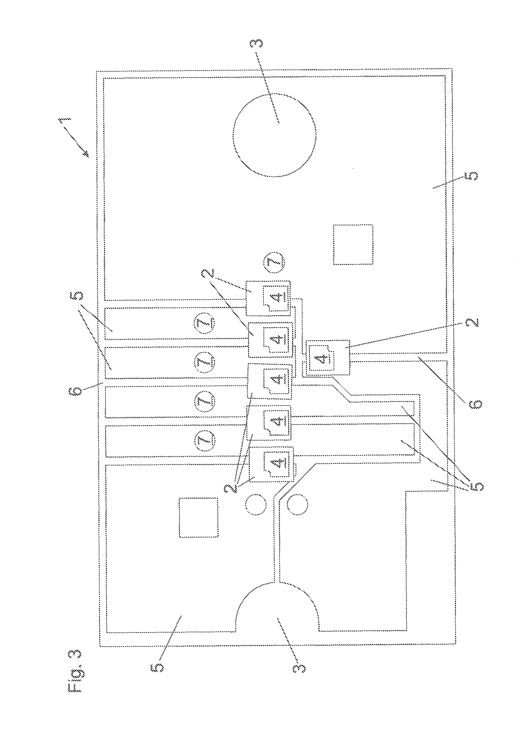
FIGS. 1 to 3 show test layouts which serve to check the positional accuracy of each individual SMD-LED 2. The circuit carrier 1 has electrically conductive surfaces 5 which are insulated from each other by insulating regions 6. The conductive surfaces 5 can be supplied with electric power by way of terminals 7.
FIG. 1 shows a circuit carrier 1 equipped with six SMD-LEDs 2. It is possible to see two reference points 3 which on the one hand serve to ascertain the deviation of the target positions for the SMD-LEDs 2 on the circuit carrier 1 and which on the other hand can also be used for fixing an optical system (not shown) for the SMD-LEDs 2. The optical system is oriented by way of separate reference points which are not shown in this Figure.
In FIG. 1 the mounting operation was effected with a "Pick & Place" and Reflow soldering process in accordance with the state of the art. In themselves the SMD-LEDs 2 are oriented by means of their outside contours relative to the reference points 3. The Reflow soldering process involves blurring of the position of the SMD-LEDs 2 so that the situation no longer involves an ordered orientation of the outside contours of the SMD-LEDs 2. Orientation in relation to the light-emitting regions 4 of the SMD-LEDs 2 has not occurred at all.
FIG. 2 shows a circuit carrier 1 equipped with six SMD-LEDs 2, the difference in relation to FIG. 1 being that the SMD-LEDs 2 are mounted on the circuit carrier 1 in the correct position in relation to the outside contour, but no mounting is effected in dependence on the light-emitting regions 4 of the SMD-LEDs 2. This circuit carrier 1 also does not meet the requirements in regard to positioning accuracy of the light-emitting regions 4.
FIG. 3 in contrast shows an embodiment by way of example of the invention in which the SMD-LEDs 2 are mounted in the correct position relative to the reference points 3 of the circuit carrier 1, on the circuit carrier 1, in regard to their light-emitting regions 4. This circuit carrier 1 meets the requirements in regard to positioning accuracy of the light-emitting regions 4.
FIGS. 4a, 4b and 4c show a process according to the invention including the steps: ascertaining the deviation in relation to the target position in the X-direction and the Y-direction of the reference point 3 i for all reference points 3 i (FIG. 4a), ascertaining the deviation in relation to the target position in the X,Y-direction and an angular position of the light-emitting region 4 of the SMD-LED 2 to be removed and in the Z-direction of the SMD-LED 2 to be removed (FIG. 4b), and mounting of the SMD-LED 2 to the circuit carrier 1 in the correct position relative to the reference points 3 i of the circuit carrier 1 (FIG. 4c).
* * * * *
References
D00000
D00001
D00002
D00003
D00004
D00005
D00006
XML
uspto.report is an independent third-party trademark research tool that is not affiliated, endorsed, or sponsored by the United States Patent and Trademark Office (USPTO) or any other governmental organization. The information provided by uspto.report is based on publicly available data at the time of writing and is intended for informational purposes only.
While we strive to provide accurate and up-to-date information, we do not guarantee the accuracy, completeness, reliability, or suitability of the information displayed on this site. The use of this site is at your own risk. Any reliance you place on such information is therefore strictly at your own risk.
All official trademark data, including owner information, should be verified by visiting the official USPTO website at www.uspto.gov. This site is not intended to replace professional legal advice and should not be used as a substitute for consulting with a legal professional who is knowledgeable about trademark law.