Method and apparatus for improved color filter saturation
Whitehead Feb
U.S. patent number 10,203,436 [Application Number 14/891,783] was granted by the patent office on 2019-02-12 for method and apparatus for improved color filter saturation. This patent grant is currently assigned to CLEARink Displays, Inc.. The grantee listed for this patent is CLEARink Displays LLC. Invention is credited to Lorne A. Whitehead.


| United States Patent | 10,203,436 |
| Whitehead | February 12, 2019 |
Method and apparatus for improved color filter saturation
Abstract
A reflective image display comprising of a reflection enhancing layer comprising of a plurality of approximately spherical indentations is placed adjacent a sheet comprising of a plurality of hemispherical protrusions. The radii of curvature of the spherical indentations substantially coincides with the center of curvature of the adjacently located hemispheres to enhance the white paper-like appearance of the display while efficiently enabling optional color filters to yield saturated color.
| Inventors: | Whitehead; Lorne A. (Vancouver, CA) | ||||||||||
|---|---|---|---|---|---|---|---|---|---|---|---|
| Applicant: |
|
||||||||||
| Assignee: | CLEARink Displays, Inc.
(Fremont, CA) |
||||||||||
| Family ID: | 51933984 | ||||||||||
| Appl. No.: | 14/891,783 | ||||||||||
| Filed: | May 15, 2014 | ||||||||||
| PCT Filed: | May 15, 2014 | ||||||||||
| PCT No.: | PCT/US2014/038091 | ||||||||||
| 371(c)(1),(2),(4) Date: | February 05, 2016 | ||||||||||
| PCT Pub. No.: | WO2014/189751 | ||||||||||
| PCT Pub. Date: | November 27, 2014 |
Prior Publication Data
| Document Identifier | Publication Date | |
|---|---|---|
| US 20160231475 A1 | Aug 11, 2016 | |
Related U.S. Patent Documents
| Application Number | Filing Date | Patent Number | Issue Date | ||
|---|---|---|---|---|---|
| 61826236 | May 22, 2013 | ||||
| Current U.S. Class: | 1/1 |
| Current CPC Class: | G02B 26/02 (20130101); G02F 1/167 (20130101); G02F 1/133553 (20130101); G02B 5/13 (20130101); G02F 1/1677 (20190101); G02F 1/133526 (20130101); G02B 5/136 (20130101); G09G 3/344 (20130101); G02B 5/201 (20130101); G02B 26/005 (20130101); G02B 26/026 (20130101); G02F 2001/1678 (20130101); G02B 5/128 (20130101) |
| Current International Class: | G02F 1/167 (20060101); G02B 5/20 (20060101); G02B 5/13 (20060101); G02B 5/136 (20060101); G02F 1/1335 (20060101); G02B 26/02 (20060101); G02B 26/00 (20060101); G02B 5/128 (20060101); G09G 3/34 (20060101) |
| Field of Search: | ;359/230 |
References Cited [Referenced By]
U.S. Patent Documents
| 3792308 | February 1974 | Ota et al. |
| 3919031 | November 1975 | White |
| 4025674 | May 1977 | Mizuochi |
| 4071430 | January 1978 | Liebert |
| 4203106 | May 1980 | Dalisa et al. |
| 4648956 | March 1987 | Marhsall et al. |
| 4821092 | April 1989 | Noguchi |
| 5019748 | May 1991 | Appelberg |
| 5319491 | June 1994 | Selbrede |
| 5359346 | October 1994 | DiSanto |
| 5396350 | March 1995 | Beeson et al. |
| 5596671 | January 1997 | Rockwell, III |
| 5871653 | February 1999 | Ling |
| 5959777 | September 1999 | Whitehead |
| 5999307 | December 1999 | Whitehead et al. |
| 6064784 | May 2000 | Whitehead et al. |
| 6215920 | April 2001 | Whitehead et al. |
| 6304365 | October 2001 | Whitehead et al. |
| 6376828 | April 2002 | Comiskey |
| 6377383 | April 2002 | Whitehead et al. |
| 6384979 | May 2002 | Whitehead et al. |
| 6437921 | August 2002 | Whitehead |
| 6452734 | September 2002 | Whitehead et al. |
| 6574025 | June 2003 | Whitehead et al. |
| 6751008 | June 2004 | Liang et al. |
| 6787976 | September 2004 | Minoura et al. |
| 6822783 | November 2004 | Matsuda et al. |
| 6842279 | January 2005 | Amundson |
| 6865011 | March 2005 | Whitehead et al. |
| 6885496 | April 2005 | Whitehead et al. |
| 6891658 | May 2005 | Whitehead et al. |
| 7046439 | May 2006 | Kaminsky et al. |
| 7093968 | August 2006 | Hsueh et al. |
| 7164536 | January 2007 | Whitehead |
| 7170670 | January 2007 | Webber |
| 7259744 | August 2007 | Arango |
| 7286280 | October 2007 | Whitehead et al. |
| 7324263 | January 2008 | Johnson et al. |
| 7422964 | September 2008 | Akiyama |
| 7439948 | October 2008 | Johnson et al. |
| 7454103 | November 2008 | Parriaux |
| 7463398 | December 2008 | Feenstra |
| 7507012 | March 2009 | Aylward et al. |
| 7515326 | April 2009 | Ibrede et al. |
| 7564614 | July 2009 | Chen et al. |
| 7660509 | February 2010 | Bryan et al. |
| 7740387 | June 2010 | Schultz et al. |
| 7760417 | July 2010 | Whitehead |
| 7775700 | August 2010 | Lee |
| 7852430 | December 2010 | Gettmey |
| 7940457 | May 2011 | Jain et al. |
| 8022615 | September 2011 | Bai et al. |
| 8040591 | October 2011 | Whitehead |
| 8094364 | January 2012 | Park |
| 8179034 | May 2012 | Potts et al. |
| 8384659 | February 2013 | Yeo et al. |
| 8587512 | November 2013 | Hiji et al. |
| 8690408 | April 2014 | Li |
| 9360696 | June 2016 | Ghali |
| 9377574 | June 2016 | Li |
| 9612501 | April 2017 | Whitehead |
| 2002/0063963 | May 2002 | Whitehead et al. |
| 2002/0089735 | July 2002 | Albert et al. |
| 2002/0171910 | November 2002 | Pullen et al. |
| 2003/0038755 | February 2003 | Amundson et al. |
| 2003/0067666 | April 2003 | Kawai |
| 2003/0165016 | September 2003 | Whitehead et al. |
| 2003/0179327 | September 2003 | Nonaka et al. |
| 2003/0214697 | November 2003 | Duthaler et al. |
| 2004/0136047 | July 2004 | Whitehead et al. |
| 2004/0174584 | September 2004 | Whitehead et al. |
| 2004/0177237 | September 2004 | Huppenthal et al. |
| 2004/0179145 | September 2004 | Jacobsen et al. |
| 2004/0239613 | December 2004 | Kishi |
| 2005/0007000 | January 2005 | Chou et al. |
| 2005/0068287 | March 2005 | Lin et al. |
| 2005/0270439 | December 2005 | Weber et al. |
| 2006/0056009 | March 2006 | Kombrekke et al. |
| 2006/0148262 | July 2006 | Lee et al. |
| 2006/0170330 | August 2006 | Disanto et al. |
| 2006/0209418 | September 2006 | Whitehead |
| 2006/0291034 | December 2006 | Patry et al. |
| 2007/0008739 | January 2007 | Kim et al. |
| 2007/0019434 | January 2007 | Lee |
| 2007/0046623 | March 2007 | Song |
| 2007/0047003 | March 2007 | Suwabe |
| 2007/0091434 | April 2007 | Garner et al. |
| 2007/0195231 | August 2007 | Kuribayashi et al. |
| 2007/0195391 | September 2007 | Nishikawa et al. |
| 2007/0263137 | November 2007 | Shigeta et al. |
| 2007/0263291 | November 2007 | Whitehead |
| 2008/0002247 | January 2008 | Nagato et al. |
| 2008/0024432 | January 2008 | Lee et al. |
| 2008/0030661 | February 2008 | Tung et al. |
| 2008/0043184 | February 2008 | Tung et al. |
| 2008/0174852 | July 2008 | Hirai et al. |
| 2008/0203910 | August 2008 | Reynolds |
| 2008/0204854 | August 2008 | Whitehead et al. |
| 2008/0218845 | September 2008 | Murakami |
| 2008/0219024 | September 2008 | Mi et al. |
| 2008/0231960 | September 2008 | Van Gorkom et al. |
| 2008/0266245 | October 2008 | Wilcox |
| 2008/0266646 | October 2008 | Wilcox et al. |
| 2008/0285282 | November 2008 | Karman et al. |
| 2008/0297496 | December 2008 | Watson et al. |
| 2008/0303994 | December 2008 | Jeng et al. |
| 2008/0304134 | December 2008 | Ban |
| 2009/0096745 | April 2009 | Sprague et al. |
| 2009/0109172 | April 2009 | Lee et al. |
| 2009/0141221 | June 2009 | Taguchi et al. |
| 2009/0201565 | August 2009 | Bita et al. |
| 2009/0201570 | August 2009 | Frazier et al. |
| 2009/0207476 | August 2009 | Yanagisawa et al. |
| 2009/0225398 | September 2009 | Duthaler et al. |
| 2009/0231714 | September 2009 | Zhao et al. |
| 2009/0244935 | October 2009 | Hsieh et al. |
| 2009/0256810 | October 2009 | Pasquariello |
| 2009/0262083 | October 2009 | Parekh |
| 2009/0262414 | October 2009 | Whitehead |
| 2009/0273746 | November 2009 | Uehara et al. |
| 2009/0322669 | December 2009 | Bryning et al. |
| 2010/0079843 | April 2010 | Derichs et al. |
| 2010/0085627 | April 2010 | Whitehead |
| 2010/0091224 | April 2010 | Cho et al. |
| 2010/0118383 | May 2010 | Van Abeelen et al. |
| 2010/0148385 | June 2010 | Balko et al. |
| 2010/0172016 | July 2010 | Park |
| 2010/0225575 | September 2010 | Ishii et al. |
| 2010/0245375 | September 2010 | Rhodes |
| 2010/0253711 | October 2010 | Muroi |
| 2011/0007381 | January 2011 | Paolini, Jr. et al. |
| 2011/0032460 | February 2011 | Lee et al. |
| 2011/0043435 | February 2011 | Hebenstreit et al. |
| 2011/0051054 | March 2011 | Wang et al. |
| 2011/0085116 | April 2011 | Kim |
| 2011/0085232 | April 2011 | Werner et al. |
| 2011/0273906 | October 2011 | Nichol et al. |
| 2011/0279442 | November 2011 | Hage et al. |
| 2011/0299014 | December 2011 | Jang et al. |
| 2011/0304902 | December 2011 | Yeo et al. |
| 2011/0310465 | December 2011 | Takanashi |
| 2011/0316764 | December 2011 | Parry-Jones et al. |
| 2012/0008203 | January 2012 | Ijzerman et al. |
| 2012/0019896 | January 2012 | Yoshida et al. |
| 2012/0019899 | January 2012 | Yeo |
| 2012/0026576 | February 2012 | Bita et al. |
| 2012/0062981 | March 2012 | Komatsu et al. |
| 2012/0069064 | March 2012 | Yamakita |
| 2012/0081777 | April 2012 | Heikenfeld et al. |
| 2012/0113367 | May 2012 | Kitson et al. |
| 2012/0113499 | May 2012 | Komatsu |
| 2012/0262496 | October 2012 | Swic |
| 2012/0287380 | November 2012 | Hagiwara et al. |
| 2012/0293857 | November 2012 | Kwon et al. |
| 2013/0050806 | February 2013 | Yasui et al. |
| 2013/0077284 | March 2013 | Chang et al. |
| 2013/0135320 | May 2013 | Govil |
| 2013/0155723 | June 2013 | Coleman |
| 2013/0182311 | July 2013 | Mochizuki et al. |
| 2013/0278995 | October 2013 | Drzaic et al. |
| 2013/0334972 | December 2013 | Atkins |
| 2014/0049448 | February 2014 | Christensen |
| 2014/0063586 | March 2014 | Jung et al. |
| 2014/0160185 | June 2014 | Okuno et al. |
| 2014/0333989 | November 2014 | Whitehead |
| 2014/0340376 | November 2014 | Itagaki et al. |
| 2015/0146273 | May 2015 | Whitehead |
| 2015/0234250 | August 2015 | Lin et al. |
| 2016/0026061 | January 2016 | O'Keeffe |
| 2016/0097961 | April 2016 | Whitehead |
| 2016/0116815 | April 2016 | Whitehead |
| 2016/0139478 | May 2016 | Whitehead et al. |
| 2016/0147128 | May 2016 | Loxley et al. |
| 2016/0155399 | June 2016 | Tripathi et al. |
| 2016/0216561 | July 2016 | Lee et al. |
| 2016/0246155 | August 2016 | Loxley et al. |
| 2016/0274435 | September 2016 | Whitehead |
| 2016/0349592 | December 2016 | Goulding et al. |
| 2016/0363811 | December 2016 | Zhong et al. |
| 2016/0377950 | December 2016 | Zhang |
| 2017/0068145 | March 2017 | Nakamura et al. |
| 2017/0075184 | March 2017 | Low et al. |
| 2017/0160444 | June 2017 | Sadlik |
| 2017/0160448 | June 2017 | Whitehead |
| 2017/0160620 | June 2017 | Whitehead |
| 2017/0287406 | October 2017 | Whitehead |
| 2017/0299935 | October 2017 | Whitehead |
| 2018/0017838 | January 2018 | Thomas |
| 2018/0031941 | February 2018 | Goulding |
| 2018/0157144 | June 2018 | Sadlik |
| 2018/0173074 | June 2018 | Zhang |
| 333109 | Aug 2006 | AT | |||
| 2292441 | Jul 2002 | CA | |||
| 2371138 | Jul 2005 | CA | |||
| 2410955 | Jan 2007 | CA | |||
| 2474384 | Aug 2010 | CA | |||
| 2643808 | Aug 2013 | CA | |||
| 1308734 | Aug 2001 | CN | |||
| 1173208 | Oct 2004 | CN | |||
| 1639625 | Jul 2005 | CN | |||
| 101160547 | Apr 2008 | CN | |||
| 1454327 | Sep 2008 | CN | |||
| 102955318 | Mar 2013 | CN | |||
| 103207495 | Jul 2013 | CN | |||
| 69825894 | Sep 2005 | DE | |||
| 1118039 | Feb 2003 | EP | |||
| 0988573 | Aug 2004 | EP | |||
| 1290486 | Oct 2004 | EP | |||
| 1368700 | Jul 2006 | EP | |||
| 2004085635 | Mar 2004 | JP | |||
| 2007505330 | Mar 2007 | JP | |||
| 3965115 | Jun 2007 | JP | |||
| 2007279641 | Oct 2007 | JP | |||
| 4113843 | Apr 2008 | JP | |||
| 2009251215 | Oct 2009 | JP | |||
| 4956610 | Mar 2012 | JP | |||
| 2005519329 | Jun 2017 | JP | |||
| 100949412 | Mar 2010 | KR | |||
| 201024886 | Jul 2010 | TW | |||
| 2003075085 | Sep 2003 | WO | |||
| 2005010604 | Feb 2005 | WO | |||
| 2006108285 | Oct 2006 | WO | |||
| 2006114743 | Nov 2006 | WO | |||
| 2008103554 | Aug 2008 | WO | |||
| 2012021121 | Feb 2012 | WO | |||
| 2014092729 | Jun 2014 | WO | |||
| 2014146937 | Sep 2014 | WO | |||
| 2014160552 | Oct 2014 | WO | |||
| 2014189751 | Nov 2014 | WO | |||
| 2015005899 | Jan 2015 | WO | |||
| 2015061538 | Apr 2015 | WO | |||
| 2015116913 | Aug 2015 | WO | |||
| 2015175518 | Nov 2015 | WO | |||
| 2016057613 | Apr 2016 | WO | |||
| 2016085835 | Jun 2016 | WO | |||
| 2016109273 | Jul 2016 | WO | |||
| 2016130720 | Aug 2016 | WO | |||
| 2007072355 | Jun 2017 | WO | |||
| 2017100157 | Jun 2017 | WO | |||
| 2017105443 | Jun 2017 | WO | |||
| 2017147449 | Aug 2017 | WO | |||
| 2017205312 | Nov 2017 | WO | |||
| 2017040628 | Mar 2018 | WO | |||
Other References
|
International Search Report and Written Opinion dated Apr. 13, 2016 for PCT Application No. PCT/US2015/066980. cited by applicant . International Search Report and Written Opinion dated Apr. 21, 2016 for PCT Application No. PCT/US2016/017416. cited by applicant . International Search Report and Written Opinion dated Mar. 1, 2016 for PCT Application No. PCT/US2015/013725. cited by applicant . International Search Report and Written Opinion dated Jan. 27, 2016 for PCT Application No. PCT/US2015/054385. cited by applicant . International Search Report and Written Opinion dated Mar. 2, 2016 for PCT Application No. PCT/US2015/062075. cited by applicant . Mossman, M. A. et al., "A Novel Reflective Image Display Using Total Internal Reflection" Displays Devices, Dempa Publications, Tokyo JP vol. 25, No. 5 Dec. 1, 2004 pp. 215-221. cited by applicant . European Patent Search Report dated Dec. 5, 2016 for EP Application No. 14800994.7. cited by applicant . International Search Report and Written Opinion dated Jul. 8, 2014 for PCT Application No. PCT/US2013/049606. cited by applicant . International Search Report and Written Opinion dated Dec. 30, 2014 for PCT Application No. PCT/US2014/058118. cited by applicant . International Search Report and Written Opinion dated Aug. 11, 2014 for PCT Application No. PCT/US2014/030966. cited by applicant . International Search Report and Written Opinion dated Sep. 19, 2014 for PCT Application No. PCT/US2014/038091. cited by applicant . International Search Report and Written Opinion dated Oct. 1, 2015 for PCT Application No. PCT/US2015/030349. cited by applicant . International Search Report and Written Opinion dated Apr. 3, 2015 for PCT Application No. PCT/US2014/061911. cited by applicant . International Search Report and Written Opinion dated Mar. 28, 2016 for PCT Application No. PCT/US2015/0066150. cited by applicant . Gou, S. et al., "Transparent Superhydrophobic Surfaces for Applications of Controlled Reflectance" Applied Optics vol. 51, Issue No. 11, Apr. 10, 2012, pp. 1645-1653. cited by applicant . Whitehead, L. et al., "The Many Roles of Illumination in Information Display" Society for Information Display Symposium (Invited Paper), Issue No. 0097-966X/06/3701-0000, May 2010. cited by applicant . Wong, R. et al., "Electrochemical Threshold Conditions During Electro-Optical Switching of Ionic Electrophorectic Optical Devices" Applied Optics vol. 48, Issue No. 6, Feb. 20, 2009, pp. 1062-1072. cited by applicant . Whitehead, L. et al., "Reflections on Total Internal Reflection" Optics and Photonics News Feb. 2009, pp. 28-34. cited by applicant . Mossman, M. et al., "Observations of Total Internal Reflection at a Natural Super-Hydrophobic Surface" Physics in Canada vol. 64, Issue No. 1, Mar. 2008, pp. 7-11. cited by applicant . Hrudey, P. et al., "Application of Transparent Nanostructured Electrodes for Modulation of Total Internal Reflection" SPIE 2007 Conference Paper No. 6647 Aug. 2007, pp. 1-12. cited by applicant . Hrudey, P. et al., "Variable Diffraction Gratings Using Nanoporous Electrodes and Electrophoresis of Dye Ions" SPIE 2007 Conference Paper No. 6645 Aug. 2007, pp. 1-12. cited by applicant . Webster, A. et al., "Control of Reflection at an Optical Interface in the Absence of Total Internal Reflection for a Retroreflective Display Application" Applied Optics vol. 45, Issue No. 6, Feb. 20, 2006, pp. 1169-1176. cited by applicant . Mossman, M. et al., "Off the Beaten Path with Total Internal Reflection" International Optical Design Conference (Invited Paper), Jun. 2006, pp. 1-12. cited by applicant . Whitehead, L. et al., "Total Internal Reflection for Illumination and Displays" SPIE Newsroom Sep. 7-8, 2006. cited by applicant . Mossman, M. et al., "Controlled Frustration of TIR by Electrophoresis of Pigment Particles" Applied Optics vol. 44, Issue No. 9, Mar. 20, 2005, pp. 1601-1609. cited by applicant . Kwong, V. et al., "Control of Reflectance of Liquid Droplets by Means of Electrowetting" Applied Optics vol. 43, Issue No. 4, Feb. 1, 2004, pp. 808-813. cited by applicant . Mossman, M. et al. "A High Reflectance, Wide Viewing Angle Reflective Display Using Total Internal Reflection in Mirco-Hemispheres" International Display Research Conference, Issue No. 1083-1312/00/2003-0233, Sep. 2003, pp. 233-236. cited by applicant . Mossman, M. et al., "Grey Scale Control of Total Internal Reflection Using Electrophoresis of Sub-Optical Pigment Particles" International Conference of the Society for Information Display, Boston, MA Issue No. 2-0966X/02/3301-0522, May 2002, pp. 522-525. cited by applicant . Coope, R. et al., "Modulation of Retroreflection by Controlled Frustration of Total Internal Reflection" Applied Optics vol. 41, Issue No. 25, Sep. 1, 2002, pp. 5357-5361. cited by applicant . Mossman, M. et al., "New Method for Maintaining Long Term Image Quality in a TIR Based Electrophoretic Display" International Display Research Conference, Nice, France, Eurodisplay Oct. 2002, pp. 851-854. cited by applicant . Mossman, M. et al., "New Reflective Color Display Technique Based on Total Internal Reflection and Subtractive Color Filtering" International Conference of the Society for Information Display, San Jose, CA Issue No. 1-0966X/01/3201-1054, Jun. 2001, pp. 1054-1057. cited by applicant . Whitehead, L. et al., "Visual Applications of Total Internal Reflection in Prismatic Microstructures" Physics in Canada Nov./Dec. 2001, pp. 329-335. cited by applicant . Mossman, M. et al., "A New Reflective Display Based on Total Internal Reflection in Prismatic Microstructures" Proceedings of the 2000 Society for Information Display, International Display Research Conference, Issue No. 1083-1312/00/2001-0311, Oct. 2000, pp. 311-314. cited by applicant . Mossman et al. "Brightness Enhancement in TIR-Modulated Electrophoretic Reflective Image Displays", (Biblio). cited by applicant . Atsuhito et al. "Electrophoresis Device, Method of Manufacturing the Electrophoresis Device, Display, Display Substrate, and Electronic Unit", (Abstract). cited by applicant . Kambe, N. et al., "Refractive Index Engineering of nano-Polymer Composites," Symposium, Apr. 20, 2001, 6 pages, Materials Research Society Symposium Proceedings, Pittsburgh, PA. cited by applicant . Robben, B. et al., "Electrodynamics of Electronic Paper Based on Total Internal Reflection," Journal, Sep. 20, 2018, pp. 034041-1-034041-11, DOI 10.1103/PhysRevApplied.10.034041, America Physical Society. cited by applicant. |
Primary Examiner: Beatty; Collin X
Attorney, Agent or Firm: Salehi; Dianoosh
Parent Case Text
RELATED APPLICATIONS
This application claims priority to Application No. PCT/US14/38091, filed May 15, 2014, under 35 U.S.C. .sctn. 371 (U.S. National Stage) which claimed the filing date benefit of U.S. Provisional Application No. 61/826,236, filed on May 22, 2013. The disclosure of each application is incorporated herein in its entirety.
Claims
What is claimed is:
1. A totally internally reflective display with a brightness enhancing structure, the display comprising: a first optically transparent sheet; at least one electrode layer; a second optically transparent sheet having a surface further comprising of a plurality of convex or hemi-spherical protrusions, each of the convex or hemi-spherical protrusions having a dark pupil region; a reflection enhancing layer that substantially semi-retro-reflects an incoming ray of light that passes through the dark pupil regions of the convex or hemi-spherical protrusions; at least one optical modulation layer wherein light is prevented or allowed to pass, the optical modulation layer including a cavity having one or more electrophoretic particles suspended in a medium; and a voltage source to controllably modulate the optical layer; wherein the outgoing light ray is substantially parallel to the incoming light ray.
2. A reflective display according to claim 1, wherein the voltage source is switchable to: apply a voltage across the optical modulation layer of one polarity to allow light to pass; and apply a voltage across the optical modulation layer of a second polarity to prevent light from passing.
3. The reflective display according to claim 2, wherein the reflection enhancing layer comprises an array of approximately spherical indentations, whereby each spherical indentation further comprises a radius of curvature that substantially coincides with the center of curvature of the convex or hemi-spherical protrusion located substantially above the array of approximately spherical indentations.
4. The reflective display according to claim 3, wherein the ratio of the radius of curvature of a spherical indentation to the radius of curvature of a hemi-spherical protrusion is about 0.5 to 5.
5. The reflective display according to claim 3, wherein the ratio of the radius of curvature of a spherical indentation to the radius of curvature of a hemi-spherical protrusion is about 1 to 3.
6. The reflective display according to claim 3, wherein the ratio of the radius of curvature of a spherical indentation to the radius of curvature of a hemi-spherical protrusion is about 1 to 2.
7. The reflective display according to claim 3, wherein the optical modulating layer is comprised of an electrophoretic medium further comprised of a plurality of suspended electrostatically charged light absorbing electrophoretically mobile particles.
8. The reflective display according to claim 3, wherein the optical modulating layer is comprised of an electro-wetting system.
9. The reflective display according to claim 3, wherein the optical modulating layer is comprised of a micro-electromechanical system.
10. The reflective display according to claim 7, wherein: movement of the electrophoretically mobile particles by application of a voltage of one polarity creates a light state; and movement of the electrophoretically mobile particles by application of a voltage of a second polarity creates a dark state.
11. The reflective display according to claim 1, further comprising a color filter array comprised of red, green and blue sub-pixels.
12. The reflective display according to claim 1, further comprising a color filter array comprised of cyan, magenta and yellow sub-pixels.
13. The reflective display according to claim 1, wherein at least one electrode layer comprises a thin film transistor array.
14. The reflective display according to claim 1, wherein at least one electrode layer comprises a patterned array.
15. The reflective display according to claim 1, further comprising spacers or spacer beads.
16. The reflective display according to claim 7, wherein the electrophoretically mobile particles are comprised of an organic material or an inorganic material or a combination of an inorganic and organic material.
17. The reflective display according to claim 7, wherein the electrophoresis medium is comprised of a hydrocarbon or a fluorocarbon or a combination of a hydrocarbon and fluorocarbon.
18. The reflective display according to claim 1, wherein the optically transparent sheet having a surface comprising of a plurality of convex protrusions or hemi-spherical protrusions may be formed by any one of embossing, etching, molding, self-assembly, printing, lithography or micro-replication.
19. The reflective display according to claim 3, wherein the reflection enhancing layer comprised of a plurality of spherical indentations may be formed by any one of embossing, etching, molding, self-assembly, printing, lithography or micro-replication.
20. The reflective display according to claim 1, further comprising a front light.
21. An electronic book reader, portable computer, tablet computer, wearable, cellular telephone, smart card, sign, watch, shelf label, flash drive, outdoor billboards or outdoor signs comprising a display according to claim 1.
Description
FIELD
This disclosure relates to a method and apparatus for improved color filter saturation. More specifically, the disclosure relates to enhanced reflective displays to produce images having a white appearance through total internal reflection.
BACKGROUND
Semi-retro-reflection refers to a reflection property of an approximately macroscopically planar structure wherein the planar structure reflects a substantial fraction of the light that strikes it, and does so with a special directional characteristic, especially for incident light that is within a range of directions deviating by less than approximately 45 degrees from the direction perpendicular to the macroscopically planar structure. The special directional characteristic is that for each incident light ray, the reflected light propagates backward in approximately the reverse direction, in other words, back towards the point of origin, with a deviation from the reverse direction that is macroscopically random and primarily less than a predetermined maximum deviation, wherein the predetermined maximum deviation being less than approximately 45 degrees. This semi-retro-reflection exhibits what is often called "optical gain", meaning that it increases the apparent reflectance of the surface under common illumination and viewing conditions. Furthermore, the manner in which light is reflected from this structure results in a paper-like white appearance. A paper-like white appearance is generally preferable to the metallic luster normally observed in optical systems that exhibit optical gain.
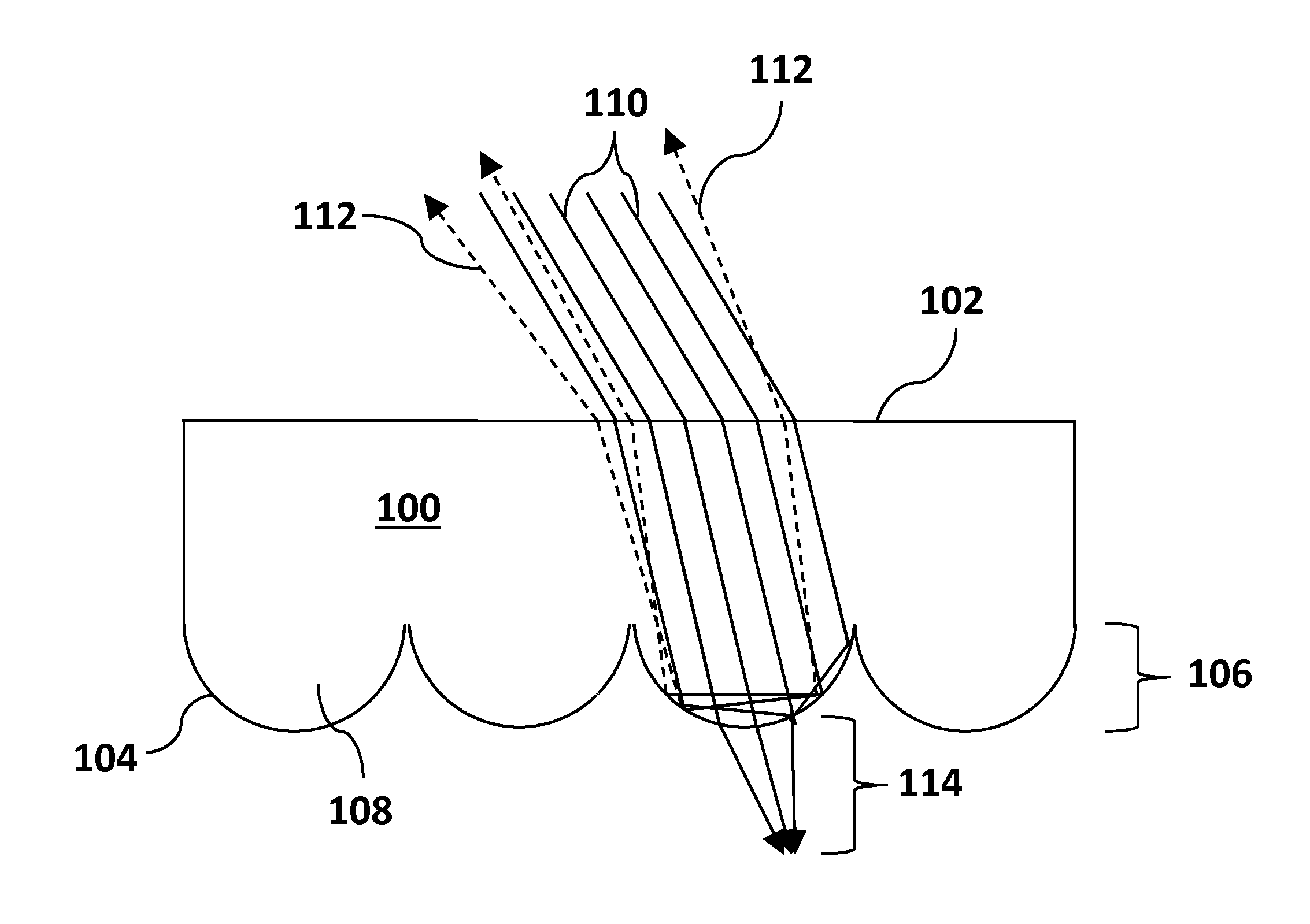
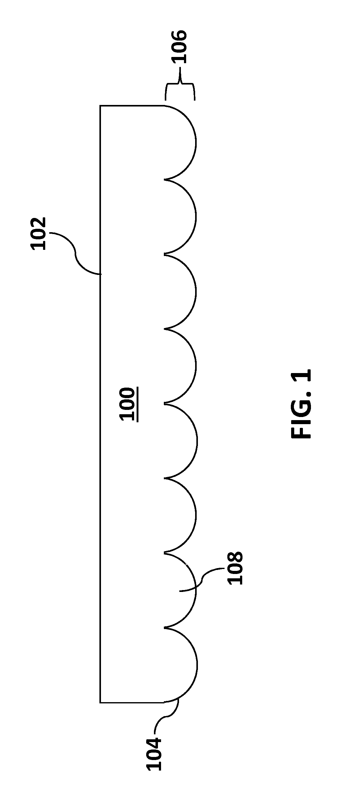
A semi-retro-reflective characteristic can be approximated in a reflective display incorporating an array of convex or hemi-spherical protrusions or hemi-spheres (it should be noted that the terms "convex protrusions" and "hemi-spherical protrusions" and "hemi-spheres" will henceforth be used interchangeably). Depicted in FIG. 1 is a front sheet 100 of a reflective display with an outward front surface 102 facing the viewer and an inward surface 104 comprising of a plurality of hemi-spherical protrusions 106 which reflects light by means of total internal reflection (TIR) within the individual hemi-spheres 108. Typically only about half of the incident light rays on sheet 100 are totally internally reflected, impeding attainment of a white appearance, as depicted in enlarged detail of a portion of a hemi-spherical array in FIG. 2. In the FIG. 2 example, the incident light rays 110 (depicted as solid lines) are either totally internally reflected and emerge as reflected light rays 112 (depicted as dotted lines) back towards the viewer or they pass through the dark pupil region as non-totally reflected light rays 114. The incident light rays 110 deviate by about 30 degrees from the perpendicular direction, which represents a typical operating condition where high quality semi-retro-reflection is desired but not achieved due to the large fraction of light rays 114 that do not undergo total internal reflection within the hemi-spheres largely due to passing through the non-reflective dark pupil region as previously explained, for example, in U.S. Pat. No. 6,885,496.
One approach to recovering a substantial portion of the light rays 114 that pass through the dark pupil region is to place a planar reflective element 116 beneath the hemi-spherical array as shown in FIG. 3 to improve reflectivity. However, although the planar reflector is able to cause most incident light rays 110 (depicted as solid lines) to undergo net reflection, most light rays reflected by the planar reflector do not have the desired semi-retro-reflection characteristic and emerge as light rays 118 (depicted as dotted lines) that instead are reflected away from the viewer and the source of incident light. High optical gain can be achieved by the system shown in FIG. 3 if the incident light rays are incident perpendicular to the hemispherical array's planar outward surface, but this has limited usefulness in practice.
Another approach to reflecting light rays that pass through the dark pupil regions of the individual convex or hemi-spherical protrusions as shown in FIG. 2 but in a semi-retro-reflective manner is to place a reflective element beneath the hemi-spherical array such that it reflects the light substantially back towards the direction of origin of the light rays. This may be achieved by a reflective element which incorporates an array of approximately spherical indentations. The approximately spherical indentations each has a radius of curvature that substantially coincides with the center of curvature of the hemi-sphere located directly above it. The invention described in this application is directed to "recycling" of such light rays in a semi-retro-reflective manner to enhance the brightness in TIR-based displays. Furthermore, the invention described enables high efficiency and high color saturation in a reflective color display comprising of a color filter array.
BRIEF DESCRIPTION OF DRAWINGS
Exemplary embodiments are illustrated in referenced figures of the drawings. It is intended that the embodiments and figures disclosed herein are to be considered illustrative rather than restrictive:
FIG. 1 illustrates a portion of an array of hemi-spherical protrusions;
FIG. 2 illustrates an array of hemi-spherical protrusions exhibiting how a portion of incident light rays are totally internally reflected and a portion that are not reflected and pass through the dark pupil region of the individual hemi-spherical protrusions;
FIG. 3 illustrates a reflective structure comprising of an array of hemi-spherical protrusions exhibiting how the portion of incident light rays that are not reflected and pass through the dark pupil region of the individual hemi-spherical protrusions are reflected with a planar reflective element;
FIG. 4 illustrates a reflective structure comprising of an array of hemi-spherical protrusions exhibiting how the portion of incident light rays that are not reflected and pass through the dark pupil region of the individual hemi-spherical protrusions are retro-reflected with a reflective element comprising of a plurality of spherical indentations;
FIG. 5 illustrates a portion of a reflective display in the light reflecting (i.e. white) state incorporating a reflective element comprising of a plurality of spherical indentations;
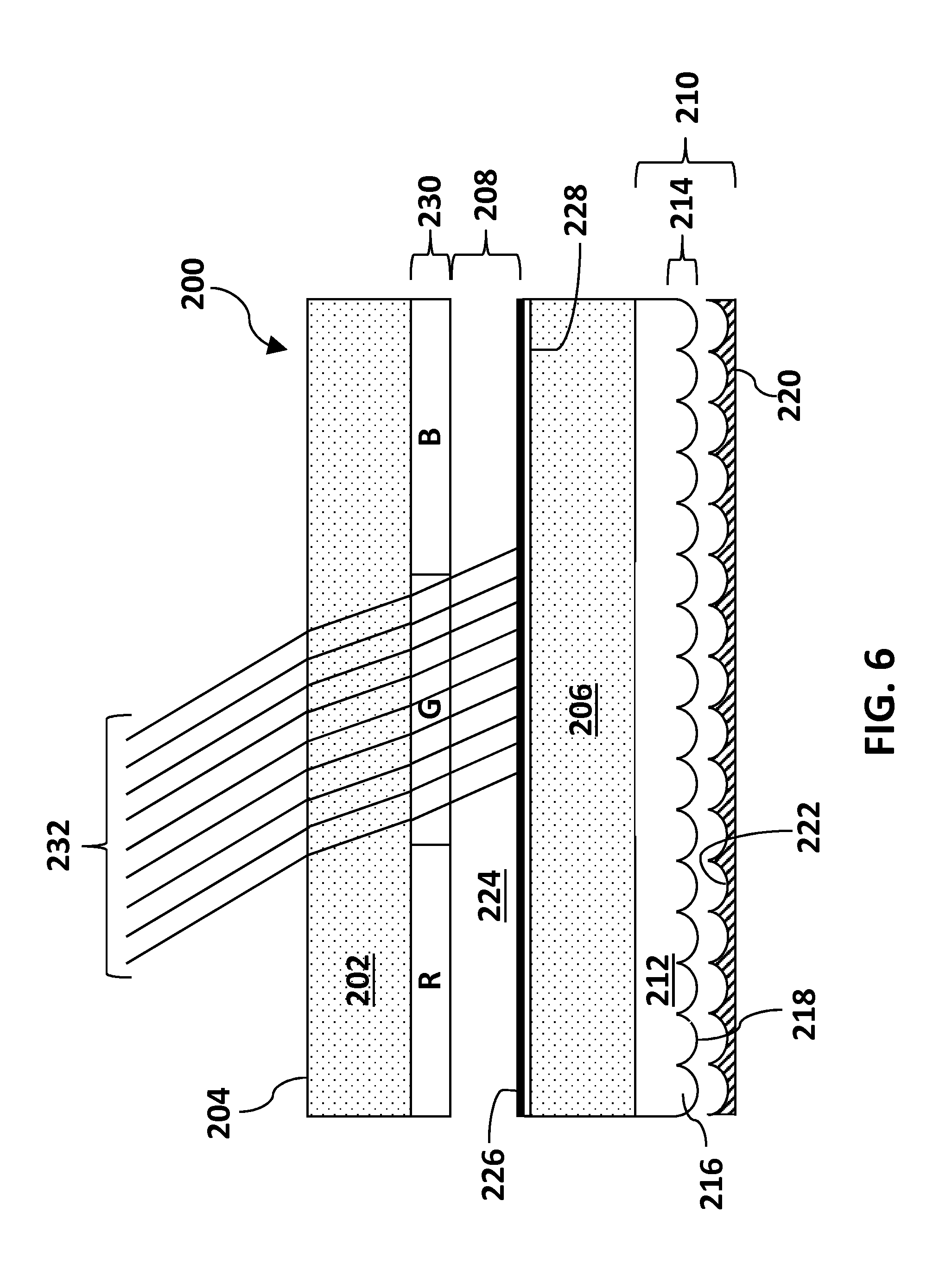
FIG. 6 illustrates a portion of a reflective display in the light absorbing (i.e. dark) state incorporating a reflective element comprising of a plurality of spherical indentations.
DESCRIPTION
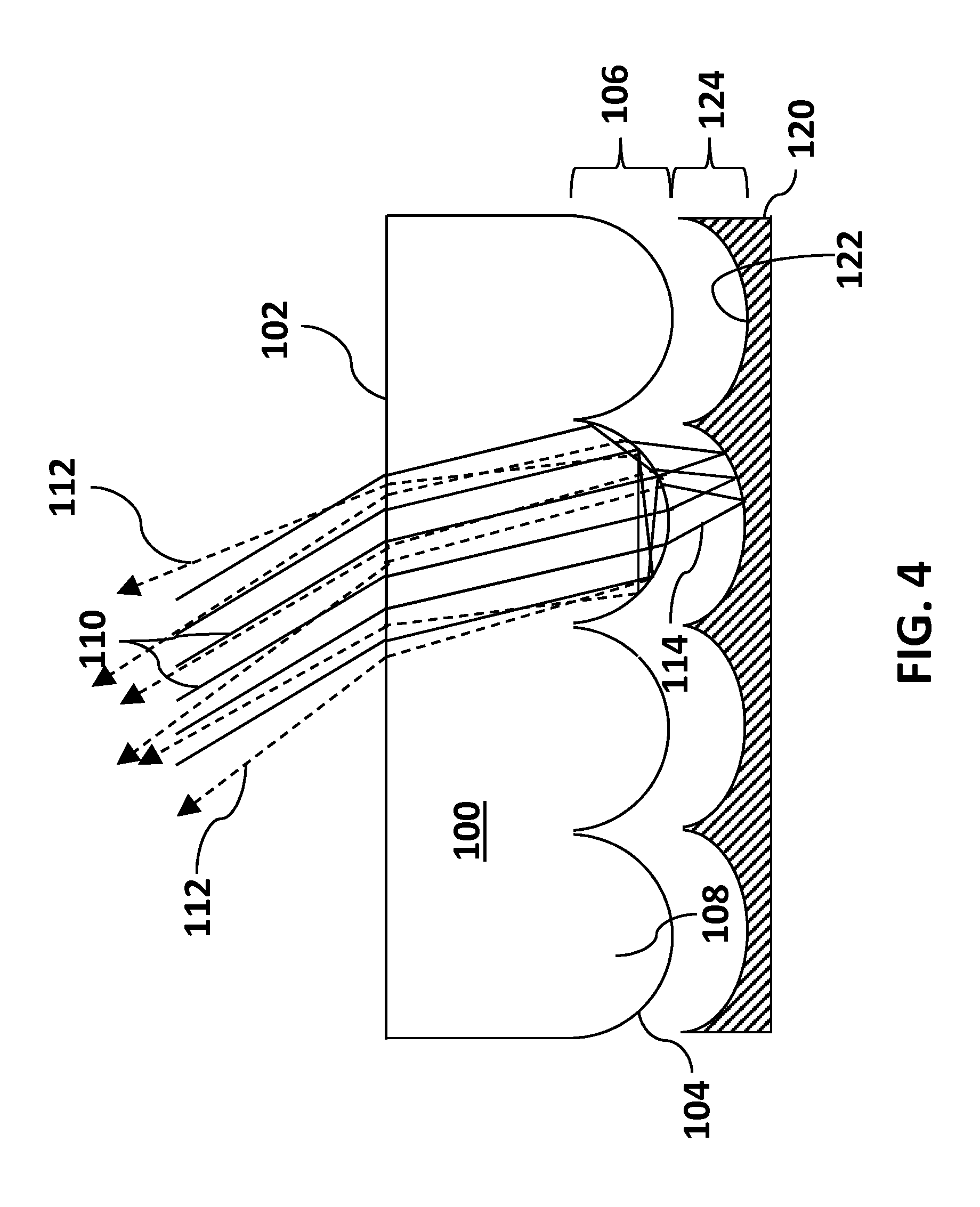
FIG. 4 depicts a reflective structure described herein in which a reflective element placed beneath the hemi-spherical array incorporates an array of approximately spherical indentations illustrating how light rays that pass through the dark pupil regions are semi-retro-reflected. FIG. 4 depicts a transparent sheet 100 with an outward surface 102 facing the viewer and an inward surface 104 opposite the viewer. Sheet 100 is further comprised of a plurality of convex protrusions or hemi-spherical protrusions or hemi-spheres 106 which reflects light by means of total internal reflection (TIR) within the individual hemi-spheres 108. Hemi-spheres 108 may also be hemi-spherical beads or hemi-beads. The reflective structure in FIG. 4 is further comprised of reflective element 120 with a reflective surface 122 placed behind sheet 100 and adjacent surface 104. Reflective element 120 is comprised of a plurality of spherical indentations 124, each of which has a radius of curvature that substantially coincides with the center of curvature of the hemi-sphere located directly above it. The ratio of the two radii of curvature influences the degree of angular deviation associated with the retro-reflection (where (radius of curvature of a spherical indentation)/(radius of curvature of a hemisphere)). Incident light rays 110 (depicted as solid lines) that pass through sheet 100 typically are totally internally reflected at the surface 104 of the hemi-spherical protrusions 108 about half of the time and are retro-reflected predominantly but not necessarily directly back towards the light source as seen in emerged light rays 112 (depicted as dotted lines). The remaining light rays that are not totally internally reflected 114 pass through the dark pupil of the individual hemi-spherical protrusions 108 and are semi-retro-reflected at the contoured surface 122 of the reflective element comprising of the plurality of spherical indentations 124. Unlike a planar reflective element described in FIG. 3 where light rays 118 are reflected away from the light source when the direction of the incident light rays is in a non-perpendicular direction to the surface of said planar reflective element, instead light rays 114 are substantially directed back towards the hemi-sphere by which they originated and emerge as light rays 112 directed towards the light source in a semi-retro-reflective manner. These light rays combine with the totally internally reflected light rays to enhance the reflectivity.
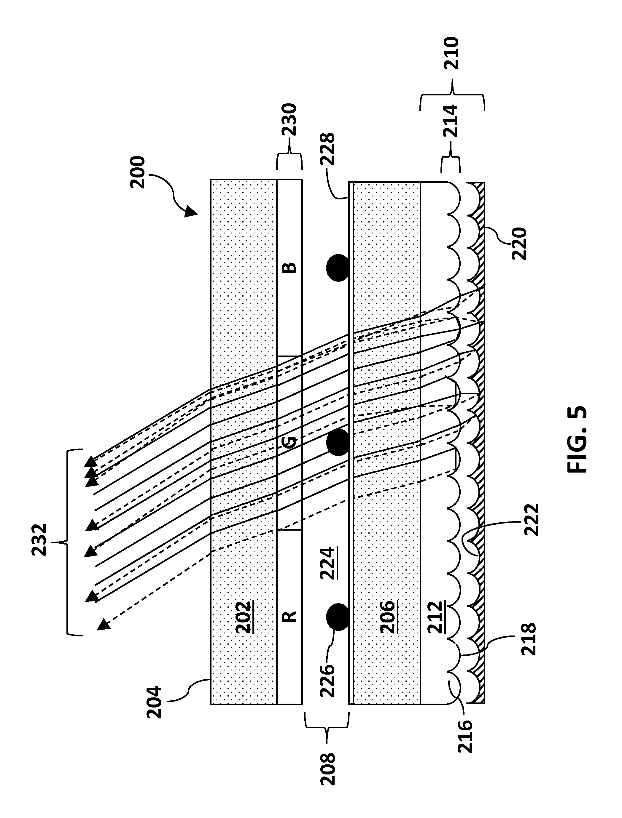
The structure described in FIG. 4 can be incorporated into a reflective display to enhance the reflectance and apparent brightness of the display. FIG. 5 embodiment depicts incorporation of a reflective structure depicted in FIG. 4 into a reflective display. Display 200 in FIG. 5 is comprised of a transparent front sheet 202 composed of, for example, glass or a polymer with an outer surface 204 facing the viewer. Display 200 further comprises a second transparent sheet 206 composed of, for example, glass or a polymer which forms a cavity 208 wherein said cavity comprises an optical modulation layer. On the opposite side of sheet 206 from cavity 208 is a rear reflective structure 210 similar to that described in FIG. 4. Reflective structure 210 is comprised of a transparent sheet 212 further comprised of a plurality of convex protrusions or hemi-spherical protrusions (i.e. hemi-spheres) 214 which reflects light by means of total internal reflection (TIR) within the individual hemi-spheres 216. The plurality of hemi-spheres 214 forms a contoured surface 218 wherein a reflective element 220 comprising of a plurality of spherical indentations with reflective surface 222 is placed adjacent. In one embodiment the ratio of the two radii of curvature is about 0.5 to 5 (where (radius of curvature of the spherical indentation)/(radius of curvature of a hemisphere).apprxeq.0.5-5). In another embodiment the ratio of the two radii of curvature is about 1 to 3. In another embodiment the ratio of the two radii of curvature is about 1 to 2. Though not shown, the display 200 in FIG. 5 may further comprise an optional front light.
The optical modulating layer 208 of display 200 in FIG. 5 allows or prevents incident light from passing through sheet 206 towards the rear reflective element 214. The optical modulating layer may be comprised of an optical shutter based on any number of techniques that do not rely on polarization of reflected light such as, but not limited to, micro-electromechanical system (MEMS), electro-wetting system or electrophoretically mobile particles or a combination thereof. Display 200 depicts an optical modulating layer comprising of a liquid medium 224 with suspended electrophoretically mobile particles 226. Within cavity 208 and located on the front surface of transparent sheet 206 is an electrode layer 228 that may be comprised of a thin film transistor array, patterned electrode array or a combination thereof. Electrode layer 228 in combination with a voltage source (not shown) controls the optical modulation layer. It may be envisioned that the electrode layer could also be located on the rear surface of the color filter layer adjacent to liquid medium 224. Display 200 further comprises an optional color filter array layer 230 further comprised of red, green and blue sub-pixels denoted R, G and B, respectively in FIG. 5. Alternatively, the sub-pixels could be composed of cyan, magenta and yellow.
As depicted in display 200 in FIG. 5, the optical modulation layer is set to transmit light. A voltage of appropriate polarity is applied such that the electrophoretically mobile particles 226 localize or group at specific locations at the electrode layer 228 such that they allow incident and reflected light rays 232 to pass. Incident light rays are depicted by the solid lines and the reflected light rays by the dotted lines. Light rays that pass through the several layers of display 200 either totally internally reflect at the convex protrusion or hemi-spherical array 214 or pass through the dark pupil regions of the individual hemi-spheres 216. The light rays that pass through the dark pupils are retro-reflected at the surface 222 of reflective element 220 such that the light rays are substantially reflected back towards the viewer from the direction by which they came (i.e. origin) thus enhancing the apparent brightness of the display.
The depiction shown in FIG. 5 illustrates an important property of the overall design described herein. Not only does it achieve high efficiency (i.e. high reflectivity of incident light rays) but the retro-reflection characteristic causes the incident light that is shown passing through the green sub-pixel filter to return substantially through the same green sub-pixel filter in the color filter layer 230 and back towards the direction of the incident light. This is critical to achieve high efficiency and high color saturation in a reflective color display. The reflective structure 210 facilitates production of a bright, white, paper-like appearance while efficiently enabling color filters to yield saturated color. These characteristics are preserved over a wide range of incident viewing angles, providing an excellent ergonomic viewing characteristic.
As depicted in display 200 in FIG. 6, the optical modulation layer comprising of a liquid medium 224 containing suspended electrophoretically mobile particles 226 is set to prevent transmission of light. In this example, the particles are delocalized into a substantially uniform layer onto the electrode layer 228 by application of an electric field of appropriate polarity such that incident light rays 232 that pass through the outer transparent sheet 202 and the optional color filter layer 230 are absorbed by the layer of particles 226 preventing light being reflected back resulting in a dark state of the display. Alternatively, one could envision the electrode layer 228 being located on the inward surface of the color filter layer 230 in display 200.
In the display embodiments described herein, they may be used in applications such as in, but not limited to, electronic book readers, portable computers, tablet computers, wearables, cellular telephones, smart cards, signs, watches, shelf labels, flash drives and outdoor billboards or outdoor signs.
Embodiments described above illustrate but do not limit this application. While a number of exemplary aspects and embodiments have been discussed above, those of skill in the art will recognize certain modifications, permutations, additions and sub-combinations thereof. Accordingly, the scope of this disclosure is defined only by the following claims.
* * * * *
D00000
D00001
D00002
D00003
D00004
D00005
D00006
XML
uspto.report is an independent third-party trademark research tool that is not affiliated, endorsed, or sponsored by the United States Patent and Trademark Office (USPTO) or any other governmental organization. The information provided by uspto.report is based on publicly available data at the time of writing and is intended for informational purposes only.
While we strive to provide accurate and up-to-date information, we do not guarantee the accuracy, completeness, reliability, or suitability of the information displayed on this site. The use of this site is at your own risk. Any reliance you place on such information is therefore strictly at your own risk.
All official trademark data, including owner information, should be verified by visiting the official USPTO website at www.uspto.gov. This site is not intended to replace professional legal advice and should not be used as a substitute for consulting with a legal professional who is knowledgeable about trademark law.