Secure lens layer
Cote Fe
U.S. patent number 10,195,890 [Application Number 15/511,316] was granted by the patent office on 2019-02-05 for secure lens layer. This patent grant is currently assigned to Crane Security Technologies, Inc.. The grantee listed for this patent is Crane Security Technologies, Inc.. Invention is credited to Paul F. Cote.


| United States Patent | 10,195,890 |
| Cote | February 5, 2019 |
Secure lens layer
Abstract
A secure lens sheet or layer suitable for use in a micro-optic system, which is made up of a plurality of joined fine lens arrays (e.g., joined fine lenticular and/or joined fine non-cylindrical lens arrays), is provided. Each array has a lens pitch different from adjacent or contiguous arrays and/or is orientated in a direction different from adjacent or contiguous arrays. A micro-optic security device, which utilizes the inventive secure lens sheet and one or more overlying or underlying arrangements of micro-sized image icons (e.g., line data), is also provided. The image icon arrangement(s) and the secure lens layer are configured such that one or more synthetic images are projected by the security device. These projected images may show a number of different optical effects. With such a combination lens layer, some regions could be optically active when the device is tilted in one direction, some could be active when tilted in the opposite direction, and some areas could be active when the device is tilted in either (or any) direction. The inventive micro-optic security device may be partially embedded in and/or mounted on a surface of a security article (e.g., paper or polymer security document, label, card), or integrated therein.
| Inventors: | Cote; Paul F. (Hollis, NH) | ||||||||||
|---|---|---|---|---|---|---|---|---|---|---|---|
| Applicant: |
|
||||||||||
| Assignee: | Crane Security Technologies,
Inc. (Nashua, NH) |
||||||||||
| Family ID: | 54200113 | ||||||||||
| Appl. No.: | 15/511,316 | ||||||||||
| Filed: | September 16, 2015 | ||||||||||
| PCT Filed: | September 16, 2015 | ||||||||||
| PCT No.: | PCT/US2015/050347 | ||||||||||
| 371(c)(1),(2),(4) Date: | March 15, 2017 | ||||||||||
| PCT Pub. No.: | WO2016/044372 | ||||||||||
| PCT Pub. Date: | March 24, 2016 |
Prior Publication Data
| Document Identifier | Publication Date | |
|---|---|---|
| US 20170246900 A1 | Aug 31, 2017 | |
Related U.S. Patent Documents
| Application Number | Filing Date | Patent Number | Issue Date | ||
|---|---|---|---|---|---|
| 62050865 | Sep 16, 2014 | ||||
| Current U.S. Class: | 1/1 |
| Current CPC Class: | G09F 3/00 (20130101); G02B 27/06 (20130101); B41M 3/146 (20130101); B42D 25/342 (20141001); G02B 3/0056 (20130101); B42D 25/324 (20141001); B44F 1/10 (20130101); B42D 25/405 (20141001); B42D 25/36 (20141001); B41M 3/142 (20130101); G02B 27/10 (20130101); B41M 3/14 (20130101); B44F 1/08 (20130101); B42D 25/30 (20141001); G02B 27/02 (20130101); B41J 2/00 (20130101); G02B 3/0068 (20130101) |
| Current International Class: | B42D 25/342 (20140101); B42D 25/36 (20140101); B42D 25/324 (20140101); B44F 1/10 (20060101); G02B 27/06 (20060101); G02B 27/10 (20060101); B42D 25/405 (20140101); G09F 3/00 (20060101); G02B 3/00 (20060101); B44F 1/08 (20060101); B41M 3/14 (20060101); B42D 25/30 (20140101); B41J 2/00 (20060101); G02B 27/02 (20060101) |
| Field of Search: | ;359/619-623,454,455 ;283/72-77,81,85 ;358/3.28 |
References Cited [Referenced By]
U.S. Patent Documents
| 992151 | May 1911 | Berthon |
| 1824353 | September 1931 | Jensen |
| 1849036 | March 1932 | Ernst |
| 1942841 | January 1934 | Shimizu |
| 2268351 | December 1941 | Tanaka |
| 2355902 | August 1944 | Berg |
| 2432896 | December 1947 | Hotchner |
| 2888855 | June 1959 | Tanaka |
| 2992103 | July 1961 | Land et al. |
| 3122853 | March 1964 | Koonz et al. |
| 3241429 | March 1966 | Rice et al. |
| 3264164 | August 1966 | Jerothe et al. |
| 3312006 | April 1967 | Rowland |
| 3357772 | December 1967 | Rowland |
| 3357773 | December 1967 | Rowland |
| 3463581 | August 1969 | Clay |
| 3609035 | September 1971 | Ataka |
| 3643361 | February 1972 | Eaves |
| 3704068 | November 1972 | Waly |
| 3801183 | April 1974 | Sevelin et al. |
| 3811213 | May 1974 | Eaves |
| 3887742 | June 1975 | Reinnagel |
| 4025673 | May 1977 | Reinnagel |
| 4073650 | February 1978 | Yevick |
| 4082426 | April 1978 | Brown |
| 4185191 | January 1980 | Stauffer |
| 4345833 | August 1982 | Siegmund |
| 4417784 | November 1983 | Knop et al. |
| 4498736 | February 1985 | Griffin |
| 4507349 | March 1985 | Fromson et al. |
| 4519632 | May 1985 | Parkinson et al. |
| 4534398 | August 1985 | Crane |
| 4634220 | January 1987 | Hockert et al. |
| 4645301 | February 1987 | Orensteen et al. |
| 4662651 | May 1987 | Mowry, Jr. |
| 4688894 | August 1987 | Hockert |
| 4691993 | September 1987 | Porter et al. |
| 4756972 | July 1988 | Kloosterboer et al. |
| 4765656 | August 1988 | Becker et al. |
| 4814594 | March 1989 | Drexler |
| 4892336 | January 1990 | Kaule et al. |
| 4892385 | January 1990 | Webster, Jr. et al. |
| 4920039 | April 1990 | Fotland et al. |
| 4935335 | June 1990 | Fotland |
| 4988126 | January 1991 | Heckenkamp et al. |
| 5044707 | September 1991 | Mallik |
| 5074649 | December 1991 | Hamanaka |
| 5085514 | February 1992 | Mallik et al. |
| 5135262 | August 1992 | Smith et al. |
| 5142383 | August 1992 | Mallik |
| 5211424 | May 1993 | Bliss |
| 5215864 | June 1993 | Laakmann |
| 5232764 | August 1993 | Oshima |
| 5254390 | October 1993 | Lu |
| 5282650 | February 1994 | Smith et al. |
| 5359454 | October 1994 | Steenblik et al. |
| 5384861 | January 1995 | Mattson et al. |
| 5393099 | February 1995 | D'Amato |
| 5393590 | February 1995 | Caspari |
| 5433807 | July 1995 | Heckenkamp et al. |
| 5449200 | September 1995 | Andric et al. |
| 5460679 | October 1995 | Abdel-Kader |
| 5461495 | October 1995 | Steenblik et al. |
| 5464690 | November 1995 | Boswell |
| 5468540 | November 1995 | Lu |
| 5479507 | December 1995 | Anderson |
| 5492370 | February 1996 | Chatwin et al. |
| 5503902 | April 1996 | Steenblik et al. |
| 5538753 | July 1996 | Antes et al. |
| 5543942 | August 1996 | Mizuguchi et al. |
| 5555476 | September 1996 | Suzuki et al. |
| 5567276 | October 1996 | Boehm et al. |
| 5568313 | October 1996 | Steenblik et al. |
| 5575507 | November 1996 | Yamauchi et al. |
| 5598281 | January 1997 | Zimmerman et al. |
| 5623347 | April 1997 | Pizzanelli |
| 5623368 | April 1997 | Calderini et al. |
| 5626969 | May 1997 | Joson |
| 5631039 | May 1997 | Knight et al. |
| 5639126 | June 1997 | Dames et al. |
| 5642226 | June 1997 | Rosenthal |
| 5643678 | July 1997 | Boswell |
| 5670003 | September 1997 | Boswell |
| 5670096 | September 1997 | Lu |
| 5674580 | October 1997 | Boswell |
| 5688587 | November 1997 | Burchard et al. |
| 5695346 | December 1997 | Sekiguchi et al. |
| 5712731 | January 1998 | Drinkwater et al. |
| 5723200 | March 1998 | Oshima et al. |
| 5731064 | March 1998 | Suss |
| 5737126 | April 1998 | Lawandy |
| 5753349 | May 1998 | Boswell |
| 5759683 | June 1998 | Boswell |
| 5763349 | June 1998 | Zandona |
| 5783017 | July 1998 | Boswell |
| 5800907 | September 1998 | Yumoto |
| 5810957 | September 1998 | Boswell |
| 5812313 | September 1998 | Johansen et al. |
| 5886798 | March 1999 | Staub et al. |
| 5933276 | August 1999 | Magee |
| 5949420 | September 1999 | Terlutter |
| 5995638 | November 1999 | Amidror et al. |
| 6030691 | February 2000 | Burchard et al. |
| 6036230 | March 2000 | Farber |
| 6036233 | March 2000 | Braun et al. |
| 6060143 | May 2000 | Tompkin et al. |
| 6084713 | July 2000 | Rosenthal |
| 6089614 | July 2000 | Howland et al. |
| 6106950 | August 2000 | Searle et al. |
| 6176582 | January 2001 | Grasnick |
| 6177953 | January 2001 | Vachette et al. |
| 6179338 | January 2001 | Bergmann et al. |
| 6195150 | February 2001 | Silverbrook |
| 6256149 | July 2001 | Rolfe |
| 6256150 | July 2001 | Rosenthal |
| 6283509 | September 2001 | Braun et al. |
| 6288842 | September 2001 | Florczak et al. |
| 6301363 | October 2001 | Mowry, Jr. |
| 6302989 | October 2001 | Kaule |
| 6328342 | December 2001 | Belousov et al. |
| 6329040 | December 2001 | Oshima et al. |
| 6345104 | February 2002 | Rhoads |
| 6348999 | February 2002 | Summersgill et al. |
| 6350036 | February 2002 | Hannington et al. |
| 6369947 | April 2002 | Staub et al. |
| 6373965 | April 2002 | Liang |
| 6381071 | April 2002 | Dona et al. |
| 6396636 | May 2002 | Sawaki |
| 6404555 | June 2002 | Nishikawa |
| 6414794 | July 2002 | Rosenthal |
| 6424467 | July 2002 | Goggins |
| 6433844 | August 2002 | Li |
| 6450540 | September 2002 | Kim |
| 6467810 | October 2002 | Taylor et al. |
| 6473238 | October 2002 | Daniell |
| 6500526 | December 2002 | Hannington |
| 6542646 | April 2003 | Bar-Yona |
| 6558009 | May 2003 | Hannington et al. |
| 6587276 | July 2003 | Daniell |
| 6616803 | September 2003 | Isherwood et al. |
| 6641270 | November 2003 | Hannington et al. |
| 6671095 | December 2003 | Summersgill et al. |
| 6712399 | March 2004 | Drinkwater et al. |
| 6721101 | April 2004 | Daniell |
| 6724536 | April 2004 | Magee |
| 6726858 | April 2004 | Andrews |
| 6751024 | June 2004 | Rosenthal |
| 6761377 | July 2004 | Taylor et al. |
| 6795250 | September 2004 | Johnson et al. |
| 6803088 | October 2004 | Kaminsky et al. |
| 6819775 | November 2004 | Amidror et al. |
| 6833960 | December 2004 | Scarbrough et al. |
| 6856462 | February 2005 | Scarbrough et al. |
| 6870681 | March 2005 | Magee |
| 6900944 | May 2005 | Tomczyk |
| 6935756 | August 2005 | Sewall et al. |
| 7030997 | April 2006 | Neureuther et al. |
| 7058202 | June 2006 | Amidror |
| 7068434 | June 2006 | Florczak et al. |
| 7114750 | October 2006 | Alasia et al. |
| 7194105 | March 2007 | Hersch et al. |
| 7246824 | July 2007 | Hudson |
| 7254265 | August 2007 | Naske et al. |
| 7255911 | August 2007 | Lutz et al. |
| 7288320 | October 2007 | Steenblik et al. |
| 7333268 | February 2008 | Steenblik et al. |
| 7336422 | February 2008 | Dunn et al. |
| 7359120 | April 2008 | Raymond |
| 7372631 | May 2008 | Ozawa |
| 7389939 | June 2008 | Jones et al. |
| 7422781 | September 2008 | Gosselin |
| 7457038 | November 2008 | Dolgoff |
| 7457039 | November 2008 | Raymond et al. |
| 7468842 | December 2008 | Steenblik et al. |
| 7504147 | March 2009 | Hannington |
| 7545567 | June 2009 | Tomczyk |
| 7609450 | October 2009 | Niemuth |
| 7630954 | December 2009 | Adamczyk et al. |
| 7686187 | March 2010 | Pottish et al. |
| 7712623 | May 2010 | Wentz et al. |
| 7719733 | May 2010 | Schilling et al. |
| 7738175 | June 2010 | Steenblik et al. |
| 7751608 | July 2010 | Hersch et al. |
| 7762591 | July 2010 | Schilling et al. |
| 7763179 | July 2010 | Levy et al. |
| 7812935 | October 2010 | Cowburn et al. |
| 7830627 | November 2010 | Commander et al. |
| 7849993 | December 2010 | Finkenzeller et al. |
| 8027093 | September 2011 | Commander et al. |
| 8057980 | November 2011 | Dunn et al. |
| 8149511 | April 2012 | Kaule et al. |
| 8284492 | October 2012 | Crane et al. |
| 8528941 | September 2013 | Dorfler et al. |
| 8557369 | October 2013 | Hoffmuller et al. |
| 8693101 | April 2014 | Tomczyk |
| 8739711 | June 2014 | Cote |
| 8867134 | October 2014 | Steenblik et al. |
| 8908276 | December 2014 | Holmes |
| 9019613 | April 2015 | Raymond |
| 9132690 | September 2015 | Raymond |
| 9592700 | March 2017 | Raymond |
| 9701150 | July 2017 | Raymond |
| 9802437 | October 2017 | Holmes |
| 2001/0048968 | December 2001 | Cox et al. |
| 2002/0014967 | February 2002 | Crane et al. |
| 2002/0114078 | August 2002 | Halle et al. |
| 2002/0185857 | December 2002 | Taylor et al. |
| 2003/0031861 | February 2003 | Reiter et al. |
| 2003/0112523 | June 2003 | Daniell |
| 2003/0157211 | August 2003 | Tsunetomo et al. |
| 2003/0179364 | September 2003 | Steenblik et al. |
| 2003/0183695 | October 2003 | Labrec et al. |
| 2003/0228014 | December 2003 | Alasia et al. |
| 2003/0232179 | December 2003 | Steenblik et al. |
| 2003/0234294 | December 2003 | Uchihiro et al. |
| 2004/0020086 | February 2004 | Hudson |
| 2004/0022967 | February 2004 | Lutz et al. |
| 2004/0100707 | May 2004 | Kay et al. |
| 2004/0140665 | July 2004 | Scarbrough et al. |
| 2004/0209049 | October 2004 | Bak |
| 2005/0094274 | May 2005 | Souparis |
| 2005/0104364 | May 2005 | Keller et al. |
| 2005/0161501 | July 2005 | Giering et al. |
| 2005/0180020 | August 2005 | Steenblik et al. |
| 2005/0247794 | November 2005 | Jones et al. |
| 2006/0003295 | January 2006 | Hersch et al. |
| 2006/0017979 | January 2006 | Goggins |
| 2006/0018021 | January 2006 | Tomkins et al. |
| 2006/0227427 | October 2006 | Dolgoff |
| 2007/0058260 | March 2007 | Steenblik et al. |
| 2007/0092680 | April 2007 | Chaffins et al. |
| 2007/0183045 | August 2007 | Schilling et al. |
| 2007/0183047 | August 2007 | Phillips et al. |
| 2007/0273143 | November 2007 | Crane et al. |
| 2007/0284546 | December 2007 | Ryzi et al. |
| 2007/0291362 | December 2007 | Hill et al. |
| 2008/0037131 | February 2008 | Steenblik et al. |
| 2008/0130018 | June 2008 | Steenblik et al. |
| 2008/0160226 | July 2008 | Kaule et al. |
| 2008/0182084 | July 2008 | Tompkin et al. |
| 2009/0008923 | January 2009 | Kaule et al. |
| 2009/0310470 | December 2009 | Yrjonen |
| 2009/0315316 | December 2009 | Staub et al. |
| 2010/0018644 | January 2010 | Sacks et al. |
| 2010/0068459 | March 2010 | Wang et al. |
| 2010/0109317 | May 2010 | Huffmuller et al. |
| 2010/0177094 | July 2010 | Kaule et al. |
| 2010/0182221 | July 2010 | Kaule et al. |
| 2010/0194532 | August 2010 | Kaule |
| 2010/0208036 | August 2010 | Kaule |
| 2010/0308571 | December 2010 | Steenblik et al. |
| 2010/0328922 | December 2010 | Peters et al. |
| 2011/0017498 | January 2011 | Lauffer et al. |
| 2011/0019283 | January 2011 | Steenblik et al. |
| 2012/0019607 | January 2012 | Dunn et al. |
| 2012/0033305 | February 2012 | Moon et al. |
| 2012/0098249 | April 2012 | Rahm et al. |
| 2012/0268819 | October 2012 | Commander et al. |
| 2013/0003354 | January 2013 | Meis et al. |
| 2013/0010048 | January 2013 | Dunn et al. |
| 2013/0044362 | February 2013 | Commander et al. |
| 2013/0154250 | June 2013 | Dunn et al. |
| 2014/0174306 | June 2014 | Wening et al. |
| 2014/0353959 | December 2014 | Lochbihler |
| 2014/0367957 | December 2014 | Jordan |
| 2009278275 | Jul 2012 | AU | |||
| 1126970 | Nov 2003 | CN | |||
| 101563640 | Oct 2009 | CN | |||
| 102712204 | Oct 2012 | CN | |||
| 19804858 | Aug 1999 | DE | |||
| 19932240 | Jan 2001 | DE | |||
| 10100692 | Aug 2004 | DE | |||
| 0090130 | Oct 1983 | EP | |||
| 0092691 | Nov 1983 | EP | |||
| 0118222 | Sep 1984 | EP | |||
| 0203752 | Dec 1986 | EP | |||
| 0253089 | Jan 1988 | EP | |||
| 0318717 | Jun 1989 | EP | |||
| 0415230 | Mar 1991 | EP | |||
| 0319157 | Jul 1992 | EP | |||
| 0930174 | Jul 1999 | EP | |||
| 0997750 | May 2000 | EP | |||
| 1356952 | Oct 2003 | EP | |||
| 1002640 | May 2004 | EP | |||
| 1354925 | Apr 2006 | EP | |||
| 1659449 | May 2006 | EP | |||
| 1876028 | Jan 2008 | EP | |||
| 2335937 | Jun 2011 | EP | |||
| 2162294 | Mar 2012 | EP | |||
| 2803939 | Jul 2001 | FR | |||
| 1095286 | Dec 1967 | GB | |||
| 2362493 | Nov 2001 | GB | |||
| 2490780 | Nov 2012 | GB | |||
| 41-004953 | Mar 1941 | JP | |||
| 46-022600 | Jun 1971 | JP | |||
| 04-234699 | Aug 1992 | JP | |||
| 10-035083 | Feb 1998 | JP | |||
| 10-039108 | Feb 1998 | JP | |||
| 11-501590 | Feb 1999 | JP | |||
| 11-189000 | Jul 1999 | JP | |||
| 2000-256994 | Sep 2000 | JP | |||
| 2001-055000 | Feb 2001 | JP | |||
| 2001-516899 | Oct 2001 | JP | |||
| 2001-324949 | Nov 2001 | JP | |||
| 2003-039583 | Feb 2003 | JP | |||
| 2003-165289 | Jun 2003 | JP | |||
| 2003-528349 | Sep 2003 | JP | |||
| 2004-262144 | Sep 2004 | JP | |||
| 2009-274293 | Nov 2009 | JP | |||
| 10-0194536 | Jun 1999 | KR | |||
| 2002170350000 | Mar 2001 | KR | |||
| 2003119050000 | May 2003 | KR | |||
| 1005443000000 | Jan 2006 | KR | |||
| 1005613210000 | Mar 2006 | KR | |||
| 2111125 | May 1998 | RU | |||
| 2245566 | Jan 2005 | RU | |||
| 575740 | Feb 2004 | TW | |||
| WO 1992/008998 | May 1992 | WO | |||
| WO 1993/024332 | Dec 1993 | WO | |||
| WO 1996/035971 | Nov 1996 | WO | |||
| WO 1997/019820 | Jun 1997 | WO | |||
| WO 1997/044769 | Nov 1997 | WO | |||
| WO 1998/013211 | Apr 1998 | WO | |||
| WO 1998/015418 | Apr 1998 | WO | |||
| WO 1998/026373 | Jun 1998 | WO | |||
| WO 1999/014725 | Mar 1999 | WO | |||
| WO 1999/023513 | May 1999 | WO | |||
| WO 1999/026793 | Jun 1999 | WO | |||
| WO 1999/066356 | Dec 1999 | WO | |||
| WO 2001/007268 | Feb 2001 | WO | |||
| WO 2001/011591 | Feb 2001 | WO | |||
| WO 2001/039138 | May 2001 | WO | |||
| WO 2001/053113 | Jul 2001 | WO | |||
| WO 2001/063341 | Aug 2001 | WO | |||
| WO 2001/071410 | Sep 2001 | WO | |||
| WO 2002/040291 | May 2002 | WO | |||
| WO 2002/043012 | May 2002 | WO | |||
| WO 2003/005075 | Jan 2003 | WO | |||
| WO 2003/007276 | Jan 2003 | WO | |||
| WO 2003/022598 | Mar 2003 | WO | |||
| WO 2003/053713 | Jul 2003 | WO | |||
| WO 2003/061980 | Jul 2003 | WO | |||
| WO 2003/061983 | Jul 2003 | WO | |||
| WO 2003/082598 | Oct 2003 | WO | |||
| WO 2003/098188 | Nov 2003 | WO | |||
| WO 2004/022355 | Mar 2004 | WO | |||
| WO 2004/036507 | Apr 2004 | WO | |||
| WO 2004/087430 | Oct 2004 | WO | |||
| WO 2005/106601 | Nov 2005 | WO | |||
| WO 2006/029744 | Mar 2006 | WO | |||
| WO 2007/076952 | Jul 2007 | WO | |||
| WO 2007/133613 | Nov 2007 | WO | |||
| WO 2008/000530 | Dec 2008 | WO | |||
| WO 2009/000527 | Dec 2008 | WO | |||
| WO 2009/000528 | Dec 2008 | WO | |||
| WO 2009/000529 | Dec 2008 | WO | |||
| WO 2009/121784 | Oct 2009 | WO | |||
| WO 2010/015383 | Feb 2010 | WO | |||
| WO 2010/136339 | Dec 2010 | WO | |||
| WO 2011/015384 | Feb 2011 | WO | |||
| WO 2011/051669 | May 2011 | WO | |||
| WO 2011/107793 | Sep 2011 | WO | |||
| WO 2011/122943 | Oct 2011 | WO | |||
| WO 2012/027779 | Mar 2012 | WO | |||
| WO 2012/103441 | Aug 2012 | WO | |||
| WO 2013/028534 | Feb 2013 | WO | |||
Other References
|
Article: "Spherical Lenses" (Jan. 18, 2009); pp. 1-12; retrieved from the Internet: URL:http://www.physicsinsights.org/simple_optics_spherical_lens- es-1.html. cited by applicant . Drinkwater, K. John, et al., "Development and applications of Diffractive Optical Security Devices for Banknotes and High Value Documents", Optical Security and Counterfeit Deterrence Techniques III, 2000, pp. 66-77, SPIE vol. 3973, San Jose, CA. cited by applicant . Fletcher, D.A., et al., "Near-field infrared imaging with a microfabricated solid immersion lens", Applied Physics Letters, Oct. 2, 2000, pp. 2109-2111, vol. 77, No. 14. cited by applicant . Gale, M. T., et al., Chapter 6--Replication, Micro Optics: Elements, Systems and Applications, 1997, pp. 153-177. cited by applicant . Hardwick, Bruce and Ghioghiu Ana, "Guardian Substrate as an Optical Medium for Security Devices", Optical Security and Counterfeit Deterrence Techniques III, 2000, pp. 176-179, SPIE vol. 3973, San Jose, CA. cited by applicant . Hutley, M.C., et al., "The Moire Magnifier", Pure Appl. Opt. 3, 1994, pp. 133-142, IOP Publishing Ltd., UK. cited by applicant . Hutley, M.C., "Integral Photography, Superlenses and the Moire Magnifier", European Optical Society, 1993, pp. 72-75, vol. 2, UK. cited by applicant . Hutley, M., et al., "Microlens Arrays", Physics World, Jul. 1991, pp. 27-32. cited by applicant . Kamal, H., et al., "Properties of Moire Magnifiers", Opt. Eng., Nov. 1998, pp. 3007-3014, vol. 37, No. 11. cited by applicant . Leech, Patrick W., et al., Printing via hot embossing of optically variable images in thermoplastic acrylic lacquer, Microelectronic Engineering, 2006, pp. 1961-1965, vol. 83, No. 10, Elsevier Publishers BV, Amsterdam, NL. cited by applicant . Lippmann, G., "Photgraphie--Epreuves Reversibles, Photographies Integrals", Academie des Sciences, 1908, pp. 446-451, vol. 146, Paris. cited by applicant . Liu, S., et al., "Artistic Effect and Application of Moire Patterns in Security Holograms", Applied Optics, Aug. 1995, pp. 4700-4702, vol. 34, No. 22. cited by applicant . Phillips, Roger W., et al., Security Enhancement of Holograms with Interference Coatings, Optical Security and Counterfeit Deterrence Techniques III, 2000, pp. 304-316, SPIE vol. 3973, San Jose, CA. cited by applicant . Steenblik, Richard A., et al., UNISON Micro-optic Security Film, Optical Security and Counterfeit Deterrence Techniques V, 2004, pp. 321-327, SPIE vol. 5310, San Jose, CA. cited by applicant . Van Renesse, Rudolf L., Optical Document Security, 1994, Artech House Inc., Norwood, MA. cited by applicant . Van Renesse, Rudolf L., Optical Document Security, 1998, 2nd edition, pp. 232-235, 240-241 and 320-321, Artech House Inc., Norwood, MA (ISBN 0-89006-982-4). cited by applicant . Van Renesse, Rudolf L., Optical Document Security, 2005, 3rd edition, pp. 62-169, Artech House Inc., Norwood, MA (ISBN 1-58053-258-6). cited by applicant . Wolpert, Gary R., Design and development of an effective optical variable device based security system incorporating additional synergistic security technologies, Optical Security and Counterfeit Deterrence Techniques III, 2000, pp. 55-61, SPIE vol. 3973, San Jose, CA. cited by applicant . Zhang, X., et al., "Concealed Holographic Coding for Security Applications by Using a Moire Technique", Applied Optics, Nov. 1997, pp. 8096-8097, vol. 36, No. 31. cited by applicant . Communication from a foreign patent office in a counterpart foreign application, National Intellectual Property Administration, P.R. China, "First Office Action," Application No. CN 201580061853.9, Sep. 10, 2018, 20 pages. cited by applicant. |
Primary Examiner: Ben; Loha
Parent Case Text
CROSS-REFERENCE TO RELATED APPLICATION
This application claims benefit of and priority to U.S. Provisional Patent Application No. 62/050,865, filed on Sep. 16, 2014, which is incorporated herein by reference in its entirety.
Claims
We claim:
1. A secure lens sheet or layer suitable for use in a micro-optic system, which comprises a plurality of joined fine lens arrays, wherein each array is in contact with an adjacent or contiguous array, or separated by a gap less than or equal to 1 mm, and wherein the arrays have a lens pitch of greater than or equal to 275 lenses per centimeter, wherein each array has a lens pitch different from that of an adjacent or contiguous array.
2. The secure lens sheet or layer of claim 1, wherein the plurality of joined fine lens arrays are substantially co-planar lens arrays and/or wherein each array is orientated in a direction different from that of an adjacent or contiguous array.
3. The secure lens sheet or layer of claim 2, wherein the plurality of joined fine lens arrays are selected from a group of joined fine lenticular lens arrays, joined fine non-cylindrical lens arrays, joined fine spherical lens arrays, joined fine aspherical lens arrays and combinations of joined fine lenticular lens arrays and joined fine non-cylindrical lens arrays.
4. The secure lens sheet or layer of claim 1, wherein the plurality of joined fine lens arrays are lenticular lens arrays, each lens array containing lenses arranged in a generally parallel, side-by-side orientation.
5. The secure lens sheet or layer of claim 1, wherein a thickness of the sheet or layer is less than about 30 microns.
6. The secure lens sheet or layer of claim 5, wherein the thickness of the sheet or layer is less than about 25 microns.
7. The secure lens sheet or layer of claim 5, wherein the thickness of the sheet or layer is less than about 20 microns.
8. A micro-optic security device, which comprises the secure lens sheet or layer of claim 1 and one or more overlying or underlying arrangements of micro-sized image icons, wherein the one or more image icon arrangements and the secure lens sheet or layer are configured such that one or more synthetic images are projected by the security device.
9. A secure article having opposing surfaces and comprising at least one micro-optic security device of claim 8, partially embedded in and/or mounted on a surface of the secure article, or integrated therein.
10. A secure lens sheet or layer suitable for use in a micro-optic system, which comprises a plurality of joined fine lens arrays, wherein each array has a lens pitch different from that of an adjacent or contiguous array and/or wherein each array is orientated in a direction different from that of an adjacent or contiguous array, wherein the secure lens sheet or layer is an elongate lens sheet that has a length and a width and is made up of an arrangement of: square and/or rectangle-shaped lenticular lens arrays that extend fully across its width and along its length, each lens array orientated in a direction different from that of adjacent or contiguous arrays and having the same or different lens pitch, wherein one or more lens arrays optionally have another lenticular lens array wholly or partially disposed therein; triangle-shaped lenticular lens arrays selected from a group of acute isosceles triangle-shaped lenticular lens arrays, and pairs of right isosceles triangle-shaped lenticular lens arrays that extend fully across its width and along its length, with each pair forming a square, with one lens array orientated in a direction perpendicular to the other lens array in the pair; and combinations thereof.
11. A secure lens sheet or layer, suitable for use in a micro-optic system, which comprises a plurality of joined fine lens arrays, wherein each array has a lens pitch different from that of an adjacent or contiguous array and/or wherein each array is orientated in a direction different from that of an adjacent or contiguous array, wherein at least one lens array is a regular lens array that has a fixed lens pitch that ranges from about 2000 to about 5000 lenses per inch.
12. The secure lens sheet or layer of claim 11, wherein the fixed lens pitch ranges from about 3000 to about 4000 lenses per inch.
13. A secure lens sheet or layer, suitable for use in a micro-optic system, which comprises a plurality of joined fine lens arrays, wherein each array has a lens pitch different from that of an adjacent or contiguous array and/or wherein each array is orientated in a direction different from that of an adjacent or contiguous array, wherein at least one lens array is an irregular lens array having more than one lens pitch, wherein, optionally, the irregular lens array has two lens pitches, a first lens pitch ranging from about 3000 to about 3500 lenses per inch and a second lens pitch ranging from 3500 to about 4000 lenses per inch.
14. A secure lens sheet or layer suitable for use in a micro-optic system, which comprises a plurality of joined fine lens arrays, wherein each array has a lens pitch different from that of an adjacent or contiguous array and/or wherein each array is orientated in a direction different from that of an adjacent or contiguous array, wherein the lens arrays are partially or totally embedded with a material to improve resistance of the lens arrays to optically degrading external effects.
Description
TECHNICAL FIELD
This invention relates to a secure lens layer, and more particularly to a micro-optic system that employs such a secure lens layer.
BACKGROUND
Optical materials have long been recognized as valued additions to secure articles (e.g., documents, labels, cards). These materials allow for a variety of self-authenticating optical effects thus rendering the secure article more resistant to counterfeiting.
By way of example, U.S. Pat. No. 7,333,268 to Steenblik et al. depicts a security device in the form of a micro-optic film material or structure that employs a regular two-dimensional array of lenses to enlarge micro-images. The film material or structure comprises: (a) one or more optical spacers; (b) an array of image icons positioned on one surface of the optical spacer; and (c) an array of microlenses positioned on an opposing surface of the optical spacer. The images projected by this film structure show a number of visual effects including orthoparallactic movement.
A common form of microlens enhanced surface that may be used with such film structures is a lenticular lens sheet. The lenticular lens sheet comprises a substrate with a top surface having a side-by-side array of substantially parallel refractive optical ridges (or substantially parallel reflective optical valleys) and with a bottom surface that is generally flat.
As is well known to those skilled in the art, a most important factor when designing or selecting a micro-optic security device for the security protection of an article is the security device's resistance to simulation by attempts at all levels of sophistication. Resistance to simulation is best done with methods that remain simple and obvious enough for the public to continue to be the main line of defense. The use of simple lens arrays such as packed hexagonal, square spherical and parallel cylindrical (lenticular) arrays may invite attempts to simulate the complex optical effects using commercially available lens sheets. Lenticular lens sheets are readily available up to about 200 lenses per inch (LPI) or 79 lenses per centimeter (LPCM), and are greater than or equal to approximately 125 microns in total thickness. While the thickness of these commercial lenticular lens sheets is greater than the thickness of lens layers used in a majority of micro-optic security devices for article security, the resolution of these 200 LPI lenticular lens sheets may be sufficient to satisfy the observer. It has therefore been difficult in practice to provide a highly counterfeit-resistance micro-optic security device that utilizes a lenticular lens array.
SUMMARY OF THE INVENTION
The present invention addresses this problem by providing a secure lens sheet or layer suitable for use in a micro-optic system, which is made up of a plurality of joined fine lens arrays (e.g., joined fine cylindrical (lenticular) and/or joined fine non-cylindrical lens arrays), each array having a lens pitch (LPI or LPCM) different from that of adjacent or contiguous arrays and/or is orientated in a direction different from that of adjacent or contiguous arrays.
The term "joined", as used herein, is intended to mean that each array is either in contact with adjacent or contiguous arrays, or separated by a small gap (e.g., less than or equal to about 1 millimeter (mm), preferably less than about 5 microns (.mu.)), while the term "fine" is intended to mean a lens array having a lens pitch (LPI or LPCM) of greater than or equal to about 700 LPI (275 LPCM).
In an exemplary embodiment, the lens arrays are cylindrical (lenticular) lens arrays where each lenticular lens array contains lenses arranged in a generally parallel and/or side-by-side orientation, and is substantially co-planar with the other array(s). The lenticular lenses in each array can be straight, curved, or include multiple bends (i.e., serpentine lenticular lens arrays). Each array may adopt any size or shape (e.g., square, rectangular, triangular, hexagonal), and is joined to one or more other arrays along one or more edges thereof.
In several such contemplated embodiments, the inventive lens sheet is an elongate lens sheet that has a length and a width and is made up of an arrangement of:
square and/or rectangle-shaped lenticular lens arrays that extend fully or partially across its width and along its length, each lens array orientated in a direction different from adjacent or contiguous arrays and having the same or different lens pitch, wherein one or more such arrays optionally have another lenticular lens array wholly or partially disposed therein (e.g., a smaller hexagon-shaped lenticular lens array disposed within a larger square or rectangle-shaped lenticular lens array);
triangle-shaped lenticular lens arrays including, but not limited to, acute isosceles triangle-shaped lenticular lens arrays, and pairs of right isosceles triangle-shaped lenticular lens arrays that extend fully across its width and along its length, with each pair forming a square, with one lens array orientated in a direction perpendicular to the other lens array in the pair; and
combinations thereof.
The above-referenced lenticular lens arrays may be used alone or in combination with other focusing element arrays including, but not limited to, non-cylindrical lens arrays. The non-cylindrical lens arrays may include lenses having circular, oval, or polygonal base geometries, and may be arranged in regular or random, one- or two-dimensional arrays. By way of example, an acute isosceles triangle-shaped cylindrical lens array may be positioned so as to at least partially intrude into a regular or random, two-dimensional array of lenses having a polygonal (e.g., hexagonal) base geometry. In one exemplary embodiment, a non-cylindrical lens array is disposed adjacent or contiguous to or disposed within a lenticular or cylindrical lens array. In another embodiment, the cylindrical lens array is disposed within the non-cylindrical array. As used herein, the term "disposed within" refers to an array which is either partially or fully contained within another array. For example, at least a part of a boundary or edge of one array may be contained within the boundary of another array.
In a further exemplary embodiment, the lens arrays are non-cylindrical (e.g., spherical or aspherical) lens arrays, where each non-cylindrical lens array contains lenses arranged generally as described above, and is substantially co-planar with the other array(s). Each array may adopt any size or shape, and is joined to one or more other arrays along one or more edges thereof. The non-cylindrical lens arrays may be disposed adjacent or contiguous to or may be contained partially or fully within one or more other arrays.
As noted above, the lens arrays used in the inventive lens sheet may have the same or different lens pitches (LPI or LPCM). In one exemplary embodiment, at least one lens array is a regular lens array that has a fixed lens pitch that ranges from about 2000 to about 5000 LPI, preferably from about 3000 to about 4000 LPI. The term "regular", as used herein, refers to a lens array with a uniform or fixed lens pitch. In another exemplary embodiment, at least one lens array is an irregular lens array having changing lens pitches (e.g., lens pitches which range from about 3000 to about 3500 LPI and from about 3500 to about 4000 LPI), which allows for different optical effects such as different speeds of movement. The term "irregular", as used herein, refers to a lens array with a non-uniform or changing lens pitch. The lens pitch may change either gradually or in one or more discrete steps thereby forming zones or areas of different lens pitches within the lens array. A changing lens pitch may be a uniform pitch change or a non-uniform pitch change along the length of the cylindrical or non-cylindrical lens (e.g., fan-shaped or bending).
The thickness of the inventive lens sheet is preferably less than about 30 microns, more preferably less than about 25 microns, and most preferably less than about 20 microns. As will be readily appreciated by those skilled in the art, the counterfeit-resistance of such sheets increases as the lens pitch increases and as the lens layer thickness decreases. This is due to the increased difficulty in fabrication and in achieving the required level of printing resolution and registration between the lenses and the underlying or overlying printing.
The present invention also provides a micro-optic security device, which comprises the secure lens sheet or layer described above and one or more overlying or underlying arrangements of micro-sized image icons (e.g., line data). The image icon arrangement(s) and the secure lens layer are configured such that one or more synthetic images are projected by the security device. These projected images may show a number of different optical effects. With such a combination lens layer, some regions could be active (i.e., project a synthetic image(s)) when the device is tilted in one direction, some could be active when tilted in the opposite axis, and some areas could be active when the device is tilted in either (or any) direction. The total thickness of the inventive security device may range from less than or equal to about 3 millimeters (mm) including (but not limited to) thicknesses ranging from less than about 50 microns, less than about 45 microns, from about 10 to about 40 microns, and ranges present therebetween.
The present invention further provides a secure article (e.g., paper or polymer security document, label, card) having opposing surfaces and comprising at least one micro-optic security device, as described above, partially embedded in and/or mounted on a surface of the secure article, or integrated therein.
Other features and advantages of the invention will be apparent to those of ordinary skill in the art from the following detailed description and accompanying drawings. Unless otherwise defined, all technical and scientific terms used herein have the same meaning as commonly understood by one of ordinary skill in the art to which this invention belongs. All publications, patent applications, patents and other references mentioned herein are incorporated by reference in their entirety. In case of conflict, the present specification, including definitions, will control. In addition, the materials, methods/processes, and examples are illustrative only and not intended to be limiting.
BRIEF DESCRIPTION OF THE DRAWINGS
The present disclosure may be better understood with reference to the following drawings. Matching reference numerals designate corresponding parts throughout the drawings, and components in the drawings are not necessarily to scale, emphasis instead being placed upon clearly illustrating the principles of the present disclosure. While exemplary embodiments are disclosed in connection with the drawings, there is no intent to limit the present disclosure to the embodiment or embodiments disclosed herein. On the contrary, the intent is to cover all alternatives, modifications and equivalents.
Particular features of the disclosed invention are illustrated by reference to the accompanying drawings in which:
FIG. 1 is a top planar view of an embodiment of the micro-optic security device of the present invention, where the lens layer is made up of square and rectangle-shaped lenticular lens arrays arranged in zones that extend across the width and along the length of the lens layer; and
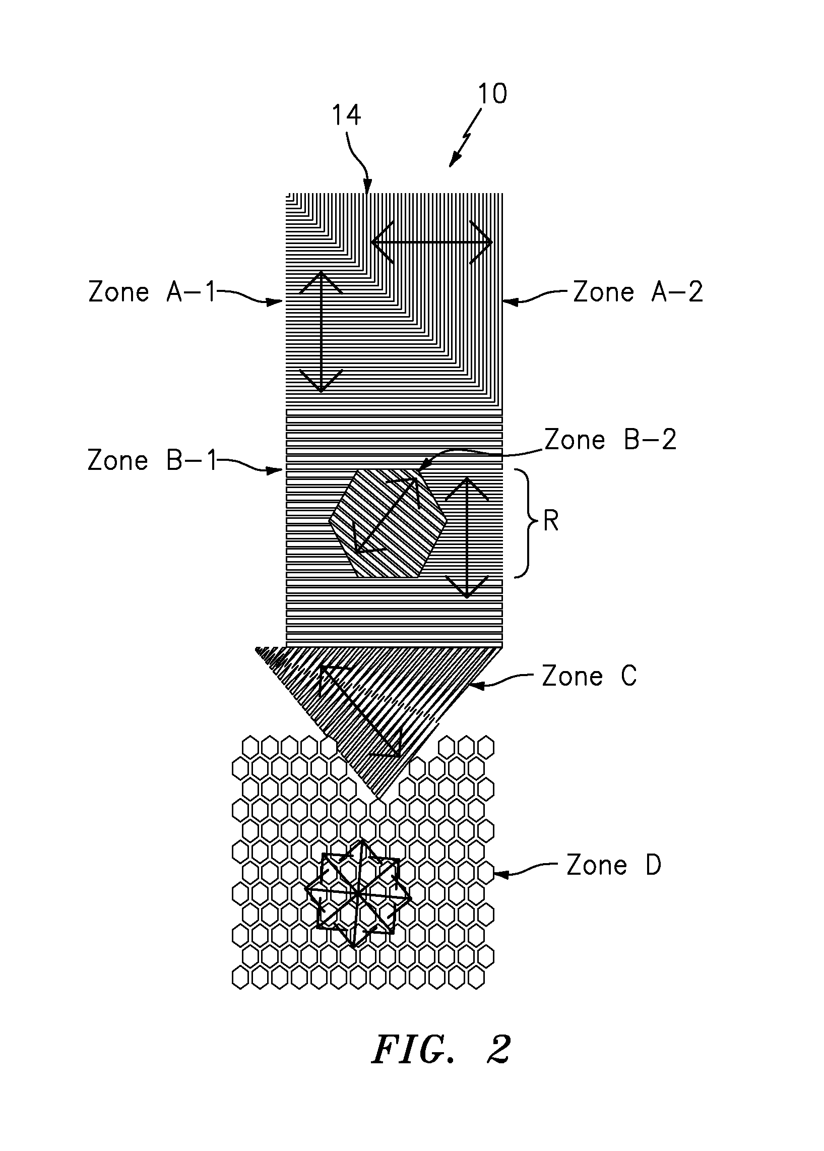
FIG. 2 is a top planar view of another embodiment of the inventive micro-optic security device where the lens layer is made up of a more intricate combination of lens arrays including both cylindrical and non-cylindrical lens arrays.
DETAILED DESCRIPTION OF THE INVENTION
By way of the present invention, both simple and intricate combinations of multiple lens arrays or formats are used on the same security device or tool. These combinations function as a major deterrent to simulating the authenticating effects generally provided by commercially available lenticular films. As noted above, with such a novel combination lens layer, some regions or zones can be active when the device is tilted in one direction, some can be active when the device is tilted in an opposite direction, while other regions or zones can be active when the device is tilted in either (or any) direction.
The secure lens sheet or layer of the present invention is made up of a plurality of joined fine lens arrays, each array being different in some way from adjacent or contiguous arrays. These differences can, for example, be orientation, lens pitch, or combinations thereof. Contemplated lens array embodiments include those made up of fine cylindrical (lenticular) lens arrays, fine non-cylindrical (e.g., spherical or aspherical) lens arrays, or a combination of both fine lenticular and fine non-cylindrical lens arrays. As noted above, it is also contemplated that individual lens arrays may have regular or irregular lens pitches. For example, a lens array may have a fixed lens pitch or it may have particular areas or zones within the array which have different pitches and/or the lens pitch may change gradually across all or part of the array. Each lens array of the plurality of joined fine lens arrays, which form the secure lens sheet or layer of the present invention, are disposed adjacent or contiguous to, or are disposed at least partially within another lens array. In one such embodiment, at least one lens array is fully disposed within another lens array, with all of its boundaries located within the boundaries of the other lens array.
Contemplated fine lenses include, but are not limited to, cylindrical and non-cylindrical refractive lenses, reflective lenses, hybrid refractive/reflective lenses, and combinations thereof.
Embedment of these lens arrays serves to improve their resistance to optically degrading external effects. In one such embodiment, the refractive index from an outer surface of the inventive lens sheet or layer to refracting interfaces is varied between a first and a second refractive index, the first refractive index being substantially or measurably different than the second refractive index. The phrase "substantially or measurably different", as used herein, means a difference in refractive index that is at least 0.04 refractive index units. The lenses can be positioned with the curved surface facing the observer and/or inverted with the curvature facing away from the observer.
The embedding material may be transparent, translucent, tinted, or pigmented and may provide additional functionality for security and authentication purposes, including support of automated currency authentication, verification, tracking, counting and detection systems, that rely on optical effects, electrical conductivity or electrical capacitance, magnetic field detection. Suitable materials can include adhesives, gels, glues, lacquers, liquids, molded polymers, and polymers or other materials containing organic or metallic dispersions.
The inventive lens sheet or layer is used with one or more overlying or underlying arrangements of micro-sized image icons or lines (e.g., line data or line patterns of specific width, angle, pitch) to form the micro-optic security device of the present invention. Here, groups of associated lens arrays and micro-sized image icons ("imaging groups") collectively form, magnify and project one or more synthetically magnified images as the device is tilted, or as the viewing angle changes. The lens arrays and the image icons (e.g., line data in the form of patterned line shaped objects) are both rotated to cause optical effects at different angles of integration to be observed. These imaging groups may project the same or different images with the same or different visual effects. Simultaneously projected images or so-called "super icons" may appear upon viewing one portion of the security device, while fixed projected images and/or sequentially projected images that change from one form to another may appear upon viewing other portions of the device. In any one location, the projected images may appear to lie on a spatial plane above or below a surface of the device, or may appear to move or turn on and off (e.g., moving bars, rotating wheels, flicker images, etc.).
As described in U.S. Pat. No. 7,333,268 to Steenblik et al., the magnitude of the magnification or synthetic magnification of the images as well as the above-noted visual effects are dependent upon the degree of "skew" between the arrangements (e.g., arrays) of focusing elements (e.g., lenses) and image icons or line data, the relative scales of the two arrays, and the f-number of the focusing elements or lenses, with the f-number being defined as the quotient obtained by dividing the focal length of the lens (f) by the effective maximum diameter of the lens (D).
One or more optical spacer layers may optionally be included between the lens arrays and micro-sized image icons or lines of the inventive micro-optic security device. This layer(s) may be formed using one or more essentially transparent or translucent polymers including, but not limited to, polycarbonate, polyester, polyethylene, polyethylene napthalate, polyethylene terephthalate, polypropylene, polyvinylidene chloride, and the like. In an exemplary embodiment, the optional optical spacer layer(s) is formed using polyester or polyethylene terephthalate.
The micro-sized image icons or lines may be printed (i.e., formed from a printing method such as ink jet, laserjet, etc.) directly on the lens layer or on the optical spacer layer. In a preferred embodiment, the image icons are raised or recessed relative to a surface of the lens or spacer layer. More specifically, the image icons are formed as either voids or recesses on or in the lens or spacer layer, or raised relative to the layer.
The secure lens layer and arrangement(s) of micro-sized image icons or lines of the inventive micro-optic security device may be formed from a variety of materials such as substantially transparent or clear, colored or colorless polymers such as acrylics, acrylated polyesters, acrylated urethanes, epoxies, polycarbonates, polypropylenes, polyesters, urethanes, and the like, using a multiplicity of methods that are known in the art of micro-optic and microstructure replication, including extrusion (e.g., extrusion embossing, soft embossing), radiation cured casting, and injection molding, reaction injection molding, and reaction casting.
An exemplary sheet or web processing method of manufacture for the micro-optic security device utilizes tools that separately incorporate the lens and image icon microstructures. In this exemplary method, both the lens tools and the icon tools are originated using photomasks and photoresist methods. The image icons are formed as voids in a radiation cured liquid polymer (e.g., acrylated urethane) that is cast against a base film (i.e., an optical spacer), such as 75 gauge adhesion-promoted polyethylene terephthalate (PET) film, then the joined fine lens arrays are formed from the radiation cured polymer on the opposite face of the base film in correct alignment or skew with respect to the image icons, then the image icon voids are filled with a submicron particle pigmented coloring material by gravure-like doctor blading against the film surface, and the fill solidified by suitable means (e.g., solvent removal, radiation curing, or chemical reaction).
Exemplary embodiments of the inventive micro-optic security device will now be described in conjunction with the drawings. A first exemplary embodiment is shown in FIG. 1, with the inventive micro-optic security device marked by reference numeral 10. Device 10 comprises elongate lens sheet or layer 12 and an underlying arrangement of micro-sized image icons or line data (not shown). Lens layer 12 is made up of square and rectangle-shaped lenticular lens arrays arranged in zones (Zones A-C) that extend fully across the width and along the length of lens layer 12. The lenses in each lens array or zone are orientated in a direction perpendicular to lenses in adjacent or contiguous zones. The lens pitch changes along the length of lens layer 12 in that the lens pitch of Zones A and C is greater than the lens pitch of Zone B.
As shown by the arrows in FIG. 1, Zone A and Zone C are optically active in that they project a synthetic image(s) that moves in the same direction when device 10 is tilted vertically. Zone B is also active in that it projects a synthetic image(s) that moves in a different direction, as shown by the arrow in Zone B, and at a reduced speed of movement due to the lower lens pitch in this zone, when the device 10 is tilted horizontally.
A second exemplary embodiment of micro-optic security device 10 is shown in FIG. 2. In this embodiment, device 10 comprises elongate lens sheet or layer 14 and an underlying arrangement of micro-sized image icons or line data (not shown). Lens layer 14 constitutes a more intricate combination of lens arrays including both cylindrical and non-cylindrical lens arrays, which are arranged in zones (Zones A-1, A-2, B-1, B-2, C, D). The lens-free areas shown in FIG. 2 may form part of a desired effect from underlying regions. For example, these areas may appear as a partial (e.g., 30%) tone of the underlying icon color without animation.
Zone A-1 and Zone A-2 constitute a pair of right isosceles triangle-shaped lenticular lens arrays, with the lenses in one array orientated in a direction perpendicular to the lenses in the other array in the pair. Together these arrays form a square that extends across the width and along the length of layer 14. Zone A-1 is active in that it projects a synthetic image(s) that moves in the direction shown by the arrow in Zone A-1 when the device 10 is tilted vertically, while Zone A-2 is active in that it projects a synthetic image(s) that moves in the direction shown by the arrow in Zone A-2 when the device 10 is tilted horizontally. Where both arrays have the same or similar lens pitch, the speed of movement of the synthetic images in these arrays would be the same or similar.
The right isosceles triangle-shaped lenticular lens array of Zone A-1 is joined to a rectangle-shaped lenticular lens array in Zone B-1, which has a smaller hexagon-shaped and obtusely angled lenticular lens array disposed therein in Zone B-2. The lenses in Zone B-1 are orientated in a direction parallel to the lenses in Zone A-1. Moreover, Zone B-1 has a lens pitch that differs from Zone A-1 and which increases in mid-region R, which is located to the right of Zone B-2. Zone B-1 is active in that it projects a synthetic image(s) that moves in the direction shown by the arrow in Zone B-1 when the device 10 is tilted vertically, with this movement increasing in speed in mid-region R due to the increased lens pitch in this region. Zone B-2 is active when the device 10 is tilted from top-right to lower-left, or vice-versa. The speed of movement of synthetic images projected by Zone B-2 is similar to the speed of movement of images projected by regions above and below region R in Zone B-1.
The rectangle-shaped lenticular lens array in Zone B-1 is joined to an acute isosceles triangle-shaped lens array in Zone C, which extends further across the width of device 10. The lenses in Zone C are orientated at an acute angle relative to the lenses in Zone B-1. Zone C has a lens pitch that increases in the direction of decreasing lens length. Zone C is active when the device 10 is tilted from top-left to lower-right, or vice-versa, with speed of movement optionally increasing as the pitch decreases.
The acute isosceles triangle-shaped lens array in Zone C intrudes partially into a regular, two-dimensional array of lenses having an hexagonal base geometry in Zone D. This array extends further across the width of device 10. As shown by the arrows in Zone D, this array is active in all directions of tilt. This array can be a regular (fixed) or an irregular (changing) array in angle and/or pitch.
As noted above, the micro-optic security device of the present invention may be partially embedded in and/or mounted on a surface of a secure article, or integrated therein. Secure articles include, but are not limited to, paper and polymer security documents, labels and cards.
While various embodiments of the present invention have been described above, it should be understood that they have been presented by way of example only, and not limitation. Thus, the breadth and scope of the present invention should not be limited by any of the exemplary embodiments.
* * * * *
References
D00000
D00001
D00002
XML
uspto.report is an independent third-party trademark research tool that is not affiliated, endorsed, or sponsored by the United States Patent and Trademark Office (USPTO) or any other governmental organization. The information provided by uspto.report is based on publicly available data at the time of writing and is intended for informational purposes only.
While we strive to provide accurate and up-to-date information, we do not guarantee the accuracy, completeness, reliability, or suitability of the information displayed on this site. The use of this site is at your own risk. Any reliance you place on such information is therefore strictly at your own risk.
All official trademark data, including owner information, should be verified by visiting the official USPTO website at www.uspto.gov. This site is not intended to replace professional legal advice and should not be used as a substitute for consulting with a legal professional who is knowledgeable about trademark law.