SFP cable connector capable of protecting solder joints
Chow , et al. Ja
U.S. patent number 10,193,268 [Application Number 15/798,426] was granted by the patent office on 2019-01-29 for sfp cable connector capable of protecting solder joints. This patent grant is currently assigned to TERALUX TECHNOLOGY CO., LTD.. The grantee listed for this patent is Teralux Technology Co., Ltd.. Invention is credited to Min-Chan Chow, Jin Hua Meng.


| United States Patent | 10,193,268 |
| Chow , et al. | January 29, 2019 |
SFP cable connector capable of protecting solder joints
Abstract
An SFP cable connector capable of protecting solder joints includes a lower case, a cable, a circuit board that is soldered with one end of the cable to form a plurality of solder joints, an insulator being formed on the circuit board and covering said solder joints, and an upper case being mounted on the lower case and being capable of pressing the insulator. The SFP cable connector can provide a direct protection for said solder joints by employing the upper case to press the insulator downward, thereby preventing said solder joints between the cable and the circuit board from being damaged and ensuring the quality of the SFP cable connector.
| Inventors: | Chow; Min-Chan (Kunshan, CN), Meng; Jin Hua (Kunshan, CN) | ||||||||||
|---|---|---|---|---|---|---|---|---|---|---|---|
| Applicant: |
|
||||||||||
| Assignee: | TERALUX TECHNOLOGY CO., LTD.
(Kunshan, CN) |
||||||||||
| Family ID: | 65032136 | ||||||||||
| Appl. No.: | 15/798,426 | ||||||||||
| Filed: | October 31, 2017 |
| Current U.S. Class: | 1/1 |
| Current CPC Class: | H01R 13/40 (20130101); H01R 13/516 (20130101); H01R 13/6591 (20130101); H01R 12/72 (20130101); H01R 13/5812 (20130101); H01R 12/53 (20130101) |
| Current International Class: | H01R 13/516 (20060101); H01R 13/40 (20060101); H01R 12/72 (20110101); H01R 12/53 (20110101) |
References Cited [Referenced By]
U.S. Patent Documents
| 6617939 | September 2003 | Vermeersch |
| 7056156 | June 2006 | Hanley |
| 7147502 | December 2006 | Wu |
| 7160135 | January 2007 | Wu |
| 7207823 | April 2007 | Yang |
| 7223915 | May 2007 | Hackman |
| 7232329 | June 2007 | Wu |
| 7238040 | July 2007 | Wu |
| 7297028 | November 2007 | Daikuhara |
| 7494363 | February 2009 | Wu |
| 7520757 | April 2009 | Bartholomew |
| 7540755 | June 2009 | Wu |
| 7559785 | July 2009 | Wu |
| 7559800 | July 2009 | Wu |
| 7690939 | April 2010 | Wu |
| 7771225 | August 2010 | Wu |
| 7841887 | November 2010 | Zhang |
| 7938669 | May 2011 | Li |
| 7955003 | June 2011 | Teo |
| 7957159 | June 2011 | Wu |
| 7997909 | August 2011 | Xu |
| 8035975 | October 2011 | Wu |
| 8047865 | November 2011 | Patel |
| 8057260 | November 2011 | Zhu |
| 8062052 | November 2011 | Wu |
| 8064207 | November 2011 | Wu |
| 8147255 | April 2012 | Wu |
| 8251733 | August 2012 | Wu |
| 8251735 | August 2012 | Wu |
| 8267718 | September 2012 | Straka |
| 8337243 | December 2012 | Elkhatib |
| 8353707 | January 2013 | Wang |
| 8360799 | January 2013 | Wu |
| 8388366 | March 2013 | Yang |
| 8439706 | May 2013 | Sytsma |
| 8475198 | July 2013 | Wu |
| 8475210 | July 2013 | Wang |
| 8480432 | July 2013 | Wu |
| 8506331 | August 2013 | Wu |
| 8523598 | September 2013 | Wu |
| 8537558 | September 2013 | Su |
| 8550848 | October 2013 | Wu |
| 8562373 | October 2013 | Wu |
| 8597045 | December 2013 | Zhu |
| 8599567 | December 2013 | Wu |
| 8614398 | December 2013 | Regnier |
| 8662917 | March 2014 | Wang |
| 8668515 | March 2014 | Wu |
| 8740637 | June 2014 | Wang |
| 8770990 | July 2014 | Sytsma |
| 8787025 | July 2014 | Wu |
| 8834185 | September 2014 | Wu |
| 8870598 | October 2014 | Qi |
| 8905777 | December 2014 | Zhu |
| 8911256 | December 2014 | Qiao |
| 8926339 | January 2015 | Houtz |
| 8926347 | January 2015 | Zhu |
| 8979553 | March 2015 | Lloyd |
| 8986036 | March 2015 | Lindkamp |
| 9071003 | June 2015 | Lindkamp |
| 9077107 | July 2015 | Lloyd |
| 9203171 | December 2015 | Yu |
| 9203193 | December 2015 | Hackman |
| 9246262 | January 2016 | Brown |
| 9337590 | May 2016 | Wu |
| 9373915 | June 2016 | Schulz |
| 9419367 | August 2016 | Henry |
| 9466925 | October 2016 | Rost |
| 9478910 | October 2016 | Nonen |
| 9553390 | January 2017 | Lu |
| 9560752 | January 2017 | Wu |
| 9671582 | June 2017 | Yeh |
| 9748694 | August 2017 | Nonen |
| 9774113 | September 2017 | Zhang |
| 9774146 | September 2017 | Cheng |
| 9799981 | October 2017 | Weber |
| 9882306 | January 2018 | Pao |
| 2006/0121794 | June 2006 | Hanley |
| 2006/0252311 | November 2006 | Togami |
| 2007/0117458 | May 2007 | Winker |
| 2007/0123090 | May 2007 | Kim |
| 2007/0161281 | July 2007 | Wu |
| 2007/0232091 | October 2007 | Hong |
| 2009/0137138 | May 2009 | Ohsumi |
| 2009/0147493 | June 2009 | Wu |
| 2009/0156058 | June 2009 | Wu |
| 2009/0227133 | September 2009 | Zhang |
| 2009/0291578 | November 2009 | Wu |
| 2010/0029104 | February 2010 | Patel |
| 2010/0091466 | April 2010 | Wu |
| 2010/0091467 | April 2010 | Wu |
| 2010/0210142 | August 2010 | McGrath |
| 2010/0248544 | September 2010 | Xu |
| 2010/0330841 | December 2010 | Zhang |
| 2011/0003502 | January 2011 | Li |
| 2011/0034082 | February 2011 | Zhu |
| 2011/0059645 | March 2011 | Wu |
| 2011/0081114 | April 2011 | Togami |
| 2011/0086548 | April 2011 | Wu |
| 2011/0136368 | June 2011 | Wu |
| 2011/0183535 | July 2011 | Wu |
| 2011/0195586 | August 2011 | Wu |
| 2011/0195590 | August 2011 | Wu |
| 2011/0195595 | August 2011 | Wu |
| 2011/0237112 | September 2011 | Wu |
| 2011/0250791 | October 2011 | Straka |
| 2011/0279984 | November 2011 | Su |
| 2011/0281455 | November 2011 | Wu |
| 2011/0287642 | November 2011 | Wang |
| 2011/0300735 | December 2011 | Wu |
| 2011/0304996 | December 2011 | Wu |
| 2011/0306244 | December 2011 | Zhang |
| 2012/0015544 | January 2012 | Wu |
| 2012/0015545 | January 2012 | Wu |
| 2012/0040545 | February 2012 | Wang |
| 2012/0040550 | February 2012 | Wu |
| 2012/0040551 | February 2012 | Wu |
| 2012/0040552 | February 2012 | Wu |
| 2012/0040560 | February 2012 | Wang |
| 2012/0040569 | February 2012 | Wang |
| 2012/0052712 | March 2012 | Wang |
| 2012/0058651 | March 2012 | Wang |
| 2012/0058652 | March 2012 | Wang |
| 2012/0058665 | March 2012 | Zerebilov |
| 2012/0063100 | March 2012 | Su |
| 2012/0064750 | March 2012 | Wu |
| 2012/0094515 | April 2012 | Wu |
| 2012/0129396 | May 2012 | Wang |
| 2012/0149255 | June 2012 | Wang |
| 2012/0164860 | June 2012 | Wang |
| 2012/0171903 | July 2012 | Wang |
| 2012/0190223 | July 2012 | Wu |
| 2012/0190224 | July 2012 | Wu |
| 2012/0208405 | August 2012 | Wang |
| 2012/0214324 | August 2012 | Wu |
| 2012/0214345 | August 2012 | Wu |
| 2012/0214350 | August 2012 | Wu |
| 2012/0218720 | August 2012 | Wu |
| 2012/0220152 | August 2012 | Wu |
| 2012/0282790 | November 2012 | Wang |
| 2013/0095676 | April 2013 | Wu |
| 2013/0109242 | May 2013 | Li |
| 2013/0231011 | September 2013 | Sytsma |
| 2013/0273766 | October 2013 | Lindkamp |
| 2013/0288507 | October 2013 | Zhu |
| 2013/0323959 | December 2013 | Zhu |
| 2014/0035755 | February 2014 | Ward |
| 2014/0120779 | May 2014 | Lloyd |
| 2014/0134898 | May 2014 | Wang |
| 2014/0154921 | June 2014 | Qi |
| 2014/0206230 | July 2014 | Rost |
| 2014/0322933 | October 2014 | Li |
| 2014/0322984 | October 2014 | Wu |
| 2014/0349496 | November 2014 | Zhu |
| 2015/0031245 | January 2015 | Wu |
| 2015/0031246 | January 2015 | Wu |
| 2015/0111402 | April 2015 | Hackman |
| 2015/0187461 | July 2015 | Potterf |
| 2015/0270649 | September 2015 | Blazek |
| 2015/0318634 | November 2015 | Henry |
| 2015/0318642 | November 2015 | Lee |
| 2016/0064873 | March 2016 | Bucher |
| 2016/0126660 | May 2016 | Henry |
| 2016/0149341 | May 2016 | Reed |
| 2016/0294114 | October 2016 | Nonen |
| 2016/0344143 | November 2016 | Guo |
| 2017/0040746 | February 2017 | Zhang |
| 2017/0294739 | October 2017 | Pao |
| 2017/0352452 | December 2017 | Nonen |
| 2018/0074273 | March 2018 | Wang |
| 202362501 | Aug 2012 | CN | |||
Attorney, Agent or Firm: JMB Davis Ben-David
Claims
We claim:
1. An SFP cable connector capable of protecting solder joints, comprising: a lower case having a lower receiving cavity; a cable, one end of which extends into the lower receiving cavity and the other end of which extends out of the lower case; a circuit board being fixed in the lower receiving cavity of the lower case and being soldered with the one end of the cable to form a plurality of solder joints on the circuit board; an insulator being formed on the top of the circuit board and covering all the solder joints; and an upper case being mounted on the lower case and forming an upper receiving cavity and a protruding shoulder with an end surface; wherein the protruding shoulder extends downward from the top of the upper receiving cavity, and the end surface of the protruding shoulder is capable of pressing the insulator downward firmly; and the insulator has a top surface and a horizontal bottom surface; the insulator is directly formed on the top of the circuit board; and the horizontal bottom surface of the insulator covers all the solder joints of the circuit board.
2. The SFP cable connector as claimed in claim 1, wherein the lower case has an insertion end at the front, a holding end at the rear and two parallel lower sidewalls; the lower receiving cavity is defined between the two lower sidewalls; the insertion end forms an insertion opening; and the holding end forms a pair of lower retaining holes; and the upper case has a front end, a rear end and two parallel upper sidewalls; the upper receiving cavity is defined between the two upper sidewalls; and the front rear end forms a pair of upper retaining holes; when the upper case is mounted on the lower case, the front end and the insertion end are combined together, the rear end and the holding end are combined together, and a pair of fasteners pass through the corresponding upper and lower retaining holes for fixing the upper case onto the lower case.
3. The SFP cable connector as claimed in claim 1, wherein the lower case further has a pair of positioning protrusions, which are formed on the two lower sidewalls and are protruding toward the lower receiving cavity; the circuit board further forms two cuts on two sides thereof, which can be engaged with the two positioning protrusions for fixing the circuit board in the lower case.
4. The SFP cable connector as claimed in claim 1, wherein the circuit board includes one row of conductive pads formed on the top of the circuit board and at the front of the circuit board, and one row of solder pads formed on the top of the circuit board and in rear of the conductive pads.
5. The SFP cable connector as claimed in claim 1, wherein the one end of the cable is a fixed end extending into the lower receiving cavity of the lower case, and the other end of the cable is a free end extending out of the lower case; the cable further has a multiple of conductors extending forward from the fixed end and being soldered onto the solder pads to form the solder joints on the top of the circuit board.
6. The SFP cable connector as claimed in claim 1, wherein the top surface of the insulator is step-like and is divided into an upper horizontal plane and a lower horizontal plane.
7. The SFP cable connector as claimed in claim 1, wherein the end surface of the protruding shoulder is horizontal to press the lower horizontal plane of the top surface of the insulator downward.
8. The SFP cable connector as claimed in claim 1, wherein further including a grounding shell, which surrounds and is fixed on the upper case and the lower case, and further including a locking and unlocking mechanism mounted on the lower case.
9. The SFP cable connector as claimed in claim 2, wherein the pair of fasteners are screws.
Description
CROSS-REFERENCE TO RELATED APPLICATIONS
Benefit is claimed to Chinese Patent Application No. 201710896837.2, filed Sep. 29, 2017, the contents of which are incorporated by reference herein in their entirety.
BACKGROUND OF THE INVENTION
Field of the Invention
The present invention relates to a connector technology, and more particularly to an SFP cable connector capable of protecting solder joints.
Description of the Prior Art
An SFP (Small Form-factor Pluggable) cable connector mainly includes an upper case, a lower case, a circuit board mounted in the lower case, and a cable connected to the circuit board.
Please refer to Chinese patent publication No. CN202362501U, which discloses a QSFP module structure, and FIG. 7 of which discloses that a copper cable (11) is welded onto a circuit board (5), and placed into a base (4), and then fixed by a cable clip (10) to prevent the copper cable (11) from being accidentally pulled out.
However, the above fixed mode by way of the above cable clip (10) provides only an indirect protective effect for welding (or solder joints) between the copper cable (11) and the circuit board (5). When the QSFP module structure is subjected to vibration or other external collision, the circuit board located in the base will sway slightly. This will affect the solder joints between the copper cable and the circuit board, and thus further affect the quality of signal transmission.
Hence, the prior fixed mode cannot provide reliable protect for the solder joints between the copper cable and the circuit board. It is necessary to provide a new SFP cable connector being capable of pre-pressing the solder joints and protecting directly the solder joints.
BRIEF SUMMARY OF THE INVENTION
A primary object of the present invention is to provide an SFP cable connector capable of protecting solder joints, which can protect directly the solder joints to prevent the solder joints between the cable and the circuit board from being damaged and to further ensure the product quality of the cable connector.
Other objects and advantages of the present invention may be further understood from the technical features disclosed by the present invention.
To achieve the aforementioned object or other objects of the present invention, the present invention adopts the following technical solution.
The present invention provides an SFP cable connector capable of protecting solder joints comprises a lower case having a lower receiving cavity, a cable, one end of which extends into the lower receiving cavity and the other end of which extends out of the lower case, a circuit board being fixed in the lower receiving cavity of the lower case and being soldered with the one end of the cable to form a plurality of solder joints on the circuit board, an insulator being formed on the top of the circuit board and covering all the solder joints; and an upper case being mounted on the lower case and forming an upper receiving cavity and a protruding shoulder with an end surface; wherein the protruding shoulder extends downward from the top of the upper receiving cavity, and the end surface of the protruding shoulder is capable of pressing the insulator downward firmly.
In one embodiment, the lower case has an insertion end at the front, a holding end at the rear and two parallel lower sidewalls; the lower receiving cavity is defined between the two lower sidewalls; the insertion end forms an insertion opening; and the holding end forms a pair of lower retaining holes; and the upper case has a front end, a rear end and two parallel upper sidewalls; the upper receiving cavity is defined between the two upper sidewalls; and the rear end forms a pair of upper retaining holes; when the upper case is mounted on the lower case, the front end and the insertion end are combined together, the rear end and the holding end are combined together, and a pair of fasteners pass through the corresponding upper and lower retaining holes for fixing the upper case onto the lower case.
In one embodiment, the lower case further has a pair of positioning protrusions, which are formed on the two lower sidewalls and are protruding toward the lower receiving cavity; the circuit board further forms two cuts on two sides thereof, which can be engaged with the two positioning protrusions for fixing the circuit board in the lower case.
In one embodiment, the circuit board includes one row of conductive pads formed on the top of the circuit board and at the front of the circuit board, and one row of solder pads formed on the top of the circuit board and in rear of the conductive pads.
In one embodiment, the one end of the cable is a fixed end extending into the lower receiving cavity of the lower case, and the other end of the cable is a free end extending out of the lower case; the cable further has a multiple of conductors extending forward from the fixed end and being soldered onto the solder pads to form the solder joints on the top of the circuit board.
In one embodiment, the insulator has a top surface and a horizontal bottom surface; the insulator is directly formed on the top of the circuit board; and the horizontal bottom surface of the insulator covers all the solder joints of the circuit board.
In one embodiment, the top surface of the insulator is step-like and is divided into an upper horizontal plane and a lower horizontal plane.
In one embodiment, the end surface of the protruding shoulder is horizontal to press the lower horizontal plane of the top surface of the insulator downward.
In one embodiment, the SFP cable connector further includes a grounding shell, which surrounds and is fixed on the upper case and the lower case, and further includes a locking and unlocking mechanism mounted on the lower case.
In one embodiment, the pair of fasteners are screws.
In comparison with the prior art, the SFP cable connector of the present invention disposes the insulator (or the plastic body) at the solder joints, and disposes the protruding shoulder on the upper case. The protruding shoulder can press the insulator downward firmly, so that all the solder joints can be directly protected against damage.
BRIEF DESCRIPTION OF THE DRAWINGS
FIG. 1 is a perspective schematic view of an SFP cable connector of the present invention;
FIG. 2 is an exploded view of the SFP cable connector shown in FIG. 1, wherein a grounding shell and an upper case are disassembled;
FIG. 3 is another schematic view of the SFP cable connector shown in FIG. 2 along another direction;
FIG. 4 is a disassembly schematic view of partial structures of the SFP cable connector, which mainly shows the position relationship of a cable and a circuit board;
FIG. 5 is a disassembly schematic view of partial structures of the SFP cable connector, which mainly shows the position relationship of the circuit board and a lower case;
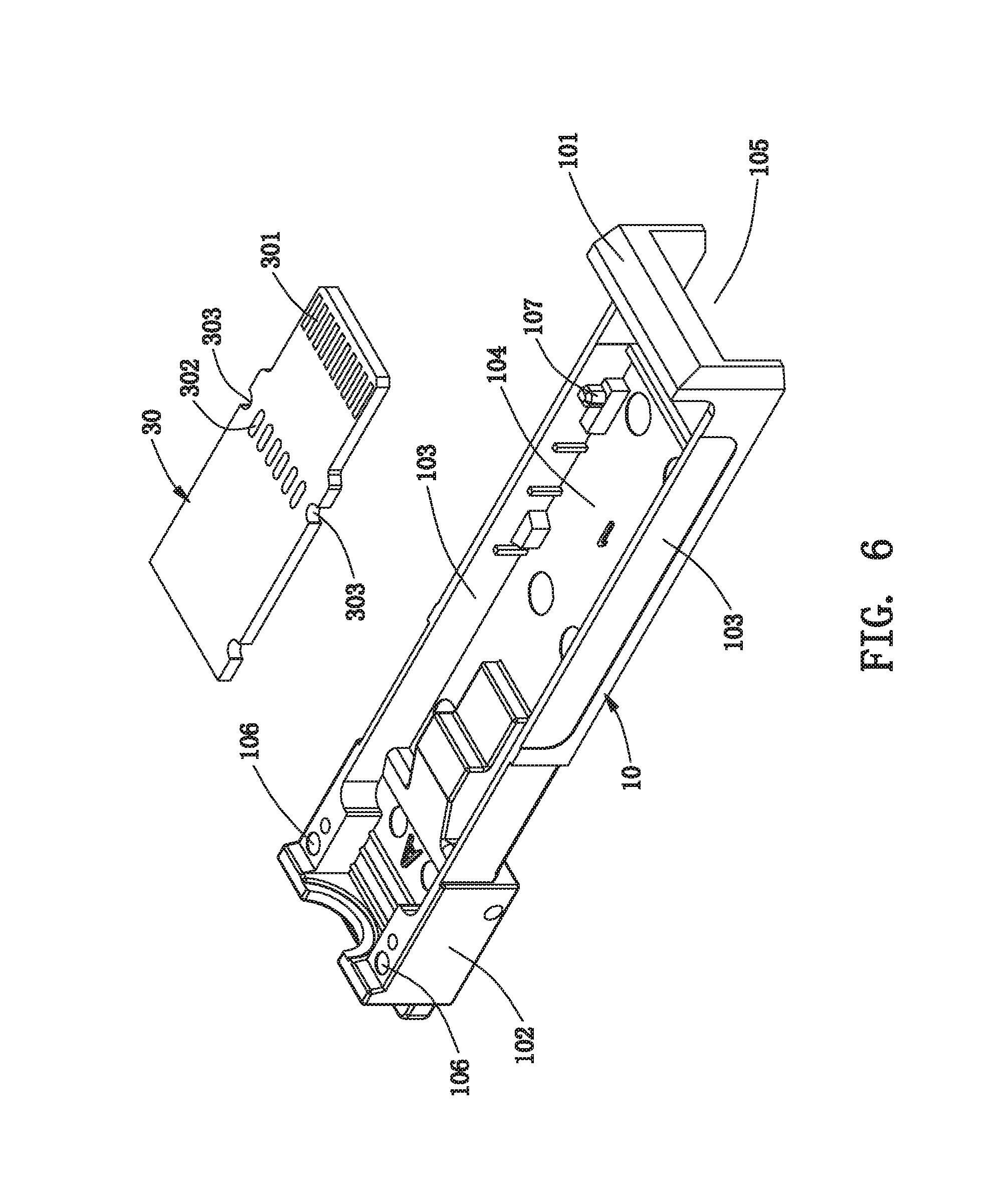
FIG. 6 shows the circuit board and the lower case of the SFP cable connector of the present invention; and
FIG. 7 is a longitudinal section view of the SFP cable connector along a line A-A of FIG. 1.
DETAILED DESCRIPTION OF THE PREFERRED EMBODIMENTS
The following description of every embodiment with reference to the accompanying drawings is used to exemplify a specific embodiment, which may be carried out in the present invention. Directional terms mentioned in the present invention, such as "up", "down", "front", "back", "left", "right", "top", "bottom" etc., are only used with reference to the orientation of the accompanying drawings. Therefore, the used directional terms are intended to illustrate, but not to limit, the present invention.
Please refer to FIGS. 1 to 7, an SFP cable connector 1 of the present invention is used to connect motherboards and fiber of network devices, such as switches, routers and other equipment.
As shown in FIGS. 1, 2 and 3, the SFP cable connector 1 of the present invention mainly comprises a lower case 10, a cable 20 extended into the lower case 10, a circuit board 30 fixed in the lower case 10 and connected to the cable 20, an insulator 40 located on the circuit board 30, and an upper case 50 being mounted on the lower case 10 and pressing the insulator 40 downward.
As shown in FIG. 6, the lower case 10 has an insertion end 101 at the front, a holding end 102 at the rear, two parallel lower sidewalls 103, and a lower receiving cavity 104 formed between the two lower sidewalls 103. In the embodiment, the insertion end 101 of the lower case 10 forms an insertion opening 105 for being used to dock with an external module (not shown). The holding end 102 forms a pair of lower retaining holes 106, and a pair of fasteners 60 (shown in FIG. 2) can pass through the corresponding lower retaining holes 106 for fixing the upper case 50 onto the lower case 10. The lower case 10 further has a pair of positioning protrusions 107, which are formed on the two lower sidewalls 103 and are protruding toward the lower receiving cavity 104 for being used to fix the circuit board 30. In the embodiment, the pair of fasteners 60 are screws.
As shown in FIG. 6, the circuit board 30 includes one row of conductive pads 301 (or gold fingers) formed on the top of the circuit board 30 and at the front of the circuit board 30, and one row of solder pads 302 formed on the top of the circuit board 30 and in rear of the conductive pads 301. In the embodiment, the circuit board 30 further forms the other row of conductive pads on the bottom of the circuit board 30. The two rows of conductive pads 301 are used to form electrical connections with the external module, and the row of solder pads 302 are used to be soldered with the cable 20. The circuit board 30 further forms two cuts 303 on two sides thereof. As shown in FIG. 5, when the circuit board 30 is placed into the lower receiving cavity 104 of the lower case 10, the positioning protrusions 107 of the lower case 10 can fit into the corresponding cuts 303 of the circuit board 30, so the circuit board 30 is fixed in the lower receiving cavity 104 of the lower case 10.
Referring to FIG. 5, the cable 20 has a fixed end 201 extending into the lower receiving cavity 104 of the lower case 10, a free end 202 extending out of the lower case 10, and a plurality of conductors 203 extending forward from the fixed end 201. As shown in FIG. 4, these conductors 203 can be soldered onto the solder pads 302 to form a plurality of solder joints 304 on the top of the circuit board 30.
Referring to FIGS. 4 and 5, the insulator 40 has a top surface 401 and a horizontal bottom surface 404. In the embodiment, the insulator 40 is a plastic body formed by the process of filling at the solder joints 304 of the circuit board 30. In the embodiment, the top surface 401 is step-like and has two stairs, which divide the top surface 401 into an upper horizontal plane 402 and a lower horizontal plane 403. But in other embodiments, the top surface 401 may form more stairs according to actual demand, or have no stair, or form a depression part thereon.
Referring to FIGS. 2 and 4, the insulator 40 is directly formed on the top of the circuit board 30. The horizontal bottom surface 404 of the insulator 40 covers all the solder joints 304 of the circuit board 30. Moreover, when assembled, the circuit board 30, all of the conductors 203 being soldered together with the circuit board 30 and the insulator 40 covering the solder joints 304 are all placed into the lower receiving cavity 104 (label seen in FIG. 6) of the lower case 10.
Please refer to FIG. 3, the upper case 50 has a construction similar to the lower case 10. The upper case 50 has a front end 501, a rear end 502, two parallel upper sidewalls 503 and an upper receiving cavity 504 formed between the two upper sidewalls 503. The upper case 50 further has a protruding shoulder 505 extending downward from the top of the upper receiving cavity 504 to be used to press the insulator 40 (label seen in FIG. 2) downward.
Please refer to FIG. 2, the rear end 502 forms a pair of upper retaining holes 506. The pair of fasteners 60 can pass through the corresponding upper retaining holes 506 firstly and then pass through the corresponding lower retaining holes 106 (label seen in FIG. 6) for fixing the upper case 50 onto the lower case 10.
Referring to FIG. 3, in the embodiment, the protruding shoulder 505 has a horizontal end surface 507. Of course, in other embodiments, the shape of the end surface 507 may be modified according to the shape of the top surface 401 of the insulator 40. For example, the end surface 507 may be step-like for matching with the stepped top surface 401 of the insulator 40 and pressing the insulator 40 downward.
Referring to FIG. 7, when the upper case 50 is mounted on the lower case 10, the front end 501 and the insertion end 101 are combined together, the rear end 502 and the holding end 102 are combined together, and the end surface 507 of the protruding shoulder 505 presses the lower horizontal plane 403 of the top surface 401 of the insulator 40 for forming a stable engaging structure. When the upper case 50 is fixed on the lower case 10 by the pair of fasteners 60, the insulator 40 can be firmly pressed by the protruding shoulder 505, thereby providing a direct protection for all the solder joints 304.
Please refer to FIGS. 1 to 3, the SFP cable connector 1 further includes a grounding shell 70 surrounding and being fixed on the upper case 50 and the lower case 10, and a locking and unlocking mechanism 80 mounted on the lower case 10.
As described above, the SFP cable connector 1 of the present invention employs the protruding shoulder 505 to press the insulator 40 downward thereby providing a direct protection for all the solder joints 304 to prevent the solder joints 304 from being damaged and ensure the SFP cable connector's quality.
It is to be understood, however, that even though numerous characteristics and advantages of the present invention have been set forth in the foregoing description, together with details of the structure and function of the invention, the disclosure is illustrative only, and changes may be made in detail, especially in matters of shape, size, and arrangement of parts within the principles of the invention to the full extent indicated by the broad general meaning of the terms in which the appended claims are expressed.
* * * * *
D00000
D00001
D00002
D00003
D00004
D00005
D00006
D00007
XML
uspto.report is an independent third-party trademark research tool that is not affiliated, endorsed, or sponsored by the United States Patent and Trademark Office (USPTO) or any other governmental organization. The information provided by uspto.report is based on publicly available data at the time of writing and is intended for informational purposes only.
While we strive to provide accurate and up-to-date information, we do not guarantee the accuracy, completeness, reliability, or suitability of the information displayed on this site. The use of this site is at your own risk. Any reliance you place on such information is therefore strictly at your own risk.
All official trademark data, including owner information, should be verified by visiting the official USPTO website at www.uspto.gov. This site is not intended to replace professional legal advice and should not be used as a substitute for consulting with a legal professional who is knowledgeable about trademark law.