Carrier aggregation low-noise amplifier with tunable integrated power splitter
Wang , et al. J
U.S. patent number 10,177,722 [Application Number 15/178,529] was granted by the patent office on 2019-01-08 for carrier aggregation low-noise amplifier with tunable integrated power splitter. This patent grant is currently assigned to QUALCOMM Incorporated. The grantee listed for this patent is QUALCOMM Incorporated. Invention is credited to Chiewcharn Narathong, Prakash Thoppay Egambaram, Mehmet Uzunkol, Chuan Wang, Kevin Hsi Huai Wang.


View All Diagrams
| United States Patent | 10,177,722 |
| Wang , et al. | January 8, 2019 |
Carrier aggregation low-noise amplifier with tunable integrated power splitter
Abstract
A device includes a low-noise amplifier (LNA) and a matching circuit. The matching circuit is coupled to an output of the LNA and switchably coupled to at least one of a first and a second output of the device. The device may further include a power splitter switchably coupled between an output of the matching circuit and the first and/or the second output of the device.
| Inventors: | Wang; Chuan (San Diego, CA), Wang; Kevin Hsi Huai (San Diego, CA), Narathong; Chiewcharn (Laguna Niguel, CA), Uzunkol; Mehmet (San Diego, CA), Thoppay Egambaram; Prakash (San Diego, CA) | ||||||||||
|---|---|---|---|---|---|---|---|---|---|---|---|
| Applicant: |
|
||||||||||
| Assignee: | QUALCOMM Incorporated (San
Diego, CA) |
||||||||||
| Family ID: | 59275135 | ||||||||||
| Appl. No.: | 15/178,529 | ||||||||||
| Filed: | June 9, 2016 |
Prior Publication Data
| Document Identifier | Publication Date | |
|---|---|---|
| US 20170201218 A1 | Jul 13, 2017 | |
Related U.S. Patent Documents
| Application Number | Filing Date | Patent Number | Issue Date | ||
|---|---|---|---|---|---|
| 62277880 | Jan 12, 2016 | ||||
| Current U.S. Class: | 1/1 |
| Current CPC Class: | H03F 1/565 (20130101); H04B 1/401 (20130101); H03F 3/195 (20130101); H03F 2200/423 (20130101); H03F 2200/378 (20130101); H03F 2200/451 (20130101); H03F 2200/294 (20130101); H04W 88/02 (20130101); H03F 2200/541 (20130101) |
| Current International Class: | H03H 7/38 (20060101); H03F 3/195 (20060101); H04B 1/401 (20150101); H03F 1/56 (20060101); H04W 88/02 (20090101) |
| Field of Search: | ;333/124-129 |
References Cited [Referenced By]
U.S. Patent Documents
| 3911364 | October 1975 | Langseth et al. |
| 4035728 | July 1977 | Ishikawa et al. |
| 4035729 | July 1977 | Perry |
| 4246655 | January 1981 | Parker |
| 4326294 | April 1982 | Okamoto et al. |
| 4715048 | December 1987 | Masamura |
| 4742563 | May 1988 | Fukumura |
| 4756023 | July 1988 | Kojima |
| 4969207 | November 1990 | Sakamoto et al. |
| 5056411 | October 1991 | Baker |
| 5128630 | July 1992 | Mijuskovic |
| 5239685 | August 1993 | Moe et al. |
| 5291519 | March 1994 | Tsurumaru |
| 5321850 | June 1994 | Backstrom et al. |
| 5345601 | September 1994 | Takagi et al. |
| 5390342 | February 1995 | Takayama et al. |
| 5559838 | September 1996 | Nakagoshi |
| 5566364 | October 1996 | Mizoguchi et al. |
| 5694396 | December 1997 | Firouzbakht et al. |
| 5697083 | December 1997 | Sano |
| 5758269 | May 1998 | Wu |
| 5761613 | June 1998 | Saunders et al. |
| 5794159 | August 1998 | Portin |
| 5805643 | September 1998 | Seki et al. |
| 5805989 | September 1998 | Ushida |
| 5835853 | November 1998 | Enoki et al. |
| 5940452 | August 1999 | Rich |
| 5999815 | December 1999 | Tenbrook et al. |
| 5999990 | December 1999 | Sharrit et al. |
| 6026288 | February 2000 | Bronner |
| 6040732 | March 2000 | Brokaw |
| 6044254 | March 2000 | Ohta et al. |
| 6063961 | May 2000 | Kroner |
| 6069923 | May 2000 | Ostman et al. |
| 6088348 | July 2000 | Bell, III et al. |
| 6208844 | March 2001 | Abdelgany |
| 6249687 | June 2001 | Thomsen et al. |
| 6407689 | June 2002 | Bazarjani et al. |
| 6424683 | July 2002 | Schollhorn |
| 6430237 | August 2002 | Anvari |
| 6472947 | October 2002 | Zeitz |
| 6473601 | October 2002 | Oda |
| 6522895 | February 2003 | Montalvo |
| 6535725 | March 2003 | Hatcher et al. |
| 6600759 | July 2003 | Wood |
| 6600907 | July 2003 | Taguchi |
| 6600931 | July 2003 | Sutton et al. |
| 6657498 | December 2003 | Park et al. |
| 6728517 | April 2004 | Sugar et al. |
| 6806777 | October 2004 | Franca-Neto |
| 6819941 | November 2004 | Dening et al. |
| 6888888 | May 2005 | Tu et al. |
| 6952594 | October 2005 | Hendin |
| 6954446 | October 2005 | Kuffner |
| 6983132 | January 2006 | Woo et al. |
| 6985712 | January 2006 | Yamakawa et al. |
| 6987950 | January 2006 | Coan |
| 7013166 | March 2006 | Clifford |
| 7023272 | April 2006 | Hung et al. |
| 7024172 | April 2006 | Murphy et al. |
| 7039377 | May 2006 | Yates |
| 7123891 | October 2006 | Loke |
| 7142042 | November 2006 | Henry |
| 7161423 | January 2007 | Paul et al. |
| 7167044 | January 2007 | Li et al. |
| 7187239 | March 2007 | Yeh |
| 7187735 | March 2007 | Kent, III et al. |
| 7187904 | March 2007 | Gainey et al. |
| 7212788 | May 2007 | Weber et al. |
| 7224231 | May 2007 | Wu |
| 7260377 | August 2007 | Burns et al. |
| 7283851 | October 2007 | Persico et al. |
| 7299021 | November 2007 | Parssinen et al. |
| 7313368 | December 2007 | Wu et al. |
| 7317894 | January 2008 | Hirose |
| 7327775 | February 2008 | Gu |
| 7333831 | February 2008 | Srinivasan et al. |
| 7356325 | April 2008 | Behzad et al. |
| 7372336 | May 2008 | Lee et al. |
| 7403508 | July 2008 | Miao |
| 7444166 | October 2008 | Sahota et al. |
| 7454181 | November 2008 | Banister et al. |
| 7477106 | January 2009 | Van Bezooijen et al. |
| 7486135 | February 2009 | Mu |
| 7495515 | February 2009 | Branch |
| 7570111 | August 2009 | Vagher et al. |
| 7599675 | October 2009 | Mu et al. |
| 7643847 | January 2010 | Daanen et al. |
| 7643848 | January 2010 | Robinett et al. |
| 7697905 | April 2010 | Lee et al. |
| 7728664 | June 2010 | Chang et al. |
| 7751513 | July 2010 | Eisenhut et al. |
| 7764726 | July 2010 | Simic et al. |
| 7848724 | December 2010 | Bult et al. |
| 7869528 | January 2011 | Robinson |
| 7877075 | January 2011 | Jin et al. |
| 7911269 | March 2011 | Yang et al. |
| 7944298 | May 2011 | Cabanillas et al. |
| 7949309 | May 2011 | Rofougaran et al. |
| 7952398 | May 2011 | Salcido et al. |
| 8008970 | August 2011 | Homol et al. |
| 8022772 | September 2011 | Cassia et al. |
| 8055229 | November 2011 | Huang |
| 8063706 | November 2011 | Li et al. |
| 8081672 | December 2011 | Kent et al. |
| 8090332 | January 2012 | Sahota et al. |
| 8090369 | January 2012 | Kitazoe |
| 8139670 | March 2012 | Son et al. |
| 8149955 | April 2012 | Tired |
| 8195117 | June 2012 | Bult et al. |
| 8208887 | June 2012 | Lee et al. |
| 8217723 | July 2012 | Rajendran et al. |
| 8242841 | August 2012 | Zhang |
| 8270499 | September 2012 | Chang et al. |
| 8270927 | September 2012 | Wallace et al. |
| 8290449 | October 2012 | Keehr et al. |
| 8295778 | October 2012 | Kotecha et al. |
| 8306494 | November 2012 | Ojo |
| 8416758 | April 2013 | Rousu et al. |
| 8442473 | May 2013 | Kaukovuori et al. |
| 8483647 | July 2013 | Kaukovuori et al. |
| 8514015 | August 2013 | Chen |
| 8571510 | October 2013 | Liu et al. |
| 8600315 | December 2013 | Roufoogaran et al. |
| 8626084 | January 2014 | Chan et al. |
| 8676148 | March 2014 | Ogasawara |
| 8706069 | April 2014 | Khoini-Poorfard et al. |
| 8774334 | July 2014 | Fernando |
| 8903343 | December 2014 | Holenstein et al. |
| 8975968 | March 2015 | Abdelhalem et al. |
| 8995591 | March 2015 | Gudem et al. |
| 9026070 | May 2015 | Persico et al. |
| 9035697 | May 2015 | Youssef et al. |
| 9059665 | June 2015 | Youssef et al. |
| 9106185 | August 2015 | Youssef et al. |
| 9124228 | September 2015 | Xu et al. |
| 9154356 | October 2015 | Tasic et al. |
| 9154357 | October 2015 | Tasic et al. |
| 9160598 | October 2015 | Davierwalla et al. |
| 9166852 | October 2015 | Davierwalla et al. |
| 9178669 | November 2015 | Fernando |
| 9431963 | August 2016 | Wang et al. |
| 9595933 | March 2017 | Zhao |
| 2002/0008575 | January 2002 | Oskowsky et al. |
| 2002/0061773 | May 2002 | Adachi et al. |
| 2002/0106010 | August 2002 | Jones |
| 2002/0111163 | August 2002 | Hamabe |
| 2002/0132597 | September 2002 | Peterzell et al. |
| 2002/0173337 | November 2002 | Hajimiri et al. |
| 2002/0193108 | December 2002 | Robinett |
| 2003/0076797 | April 2003 | Lozano |
| 2003/0081694 | May 2003 | Wieck |
| 2003/0125040 | July 2003 | Walton et al. |
| 2003/0148750 | August 2003 | Yan et al. |
| 2003/0157915 | August 2003 | Atkinson et al. |
| 2003/0176176 | September 2003 | Leinonen et al. |
| 2003/0206076 | November 2003 | Hashemi et al. |
| 2003/0228851 | December 2003 | Taniguchi |
| 2004/0087290 | May 2004 | Schmidt et al. |
| 2004/0092243 | May 2004 | Hey-Shipton |
| 2004/0113746 | June 2004 | Brindle |
| 2004/0116086 | June 2004 | Huttunen |
| 2004/0121753 | June 2004 | Sugar et al. |
| 2004/0204104 | October 2004 | Horng et al. |
| 2004/0219959 | November 2004 | Khayrallah et al. |
| 2004/0224643 | November 2004 | Nakai |
| 2004/0248532 | December 2004 | Khoini-Poorfard |
| 2004/0253955 | December 2004 | Love et al. |
| 2004/0266356 | December 2004 | Javor et al. |
| 2005/0012432 | January 2005 | Murphy |
| 2005/0039060 | February 2005 | Okayasu |
| 2005/0075077 | April 2005 | Mach et al. |
| 2005/0079847 | April 2005 | Arafa |
| 2005/0118977 | June 2005 | Drogi et al. |
| 2005/0197090 | September 2005 | Stockstad et al. |
| 2005/0215264 | September 2005 | Subramaniam et al. |
| 2005/0265084 | December 2005 | Choi |
| 2005/0277387 | December 2005 | Kojima et al. |
| 2006/0023745 | February 2006 | Koo et al. |
| 2006/0061773 | March 2006 | Lee et al. |
| 2006/0121937 | June 2006 | Son |
| 2006/0128322 | June 2006 | Igarashi et al. |
| 2006/0146693 | July 2006 | Mori et al. |
| 2006/0189286 | August 2006 | Kyu et al. |
| 2006/0222100 | October 2006 | Behzad |
| 2006/0234662 | October 2006 | Diloisy |
| 2006/0291428 | December 2006 | Filipovic |
| 2007/0049332 | March 2007 | Higuchi |
| 2007/0060080 | March 2007 | Nishimura et al. |
| 2007/0072577 | March 2007 | Rozenblit et al. |
| 2007/0105517 | May 2007 | Chang et al. |
| 2007/0142013 | June 2007 | Bucknor et al. |
| 2007/0177656 | August 2007 | Maruta et al. |
| 2007/0177693 | August 2007 | Kluge |
| 2007/0184801 | August 2007 | Kogawa et al. |
| 2007/0184811 | August 2007 | Ballantyne et al. |
| 2007/0197170 | August 2007 | Boos |
| 2007/0197178 | August 2007 | Gu |
| 2007/0197204 | August 2007 | Herczog et al. |
| 2007/0202890 | August 2007 | Feher |
| 2007/0207752 | September 2007 | Behzad |
| 2007/0242784 | October 2007 | Sampson et al. |
| 2007/0243832 | October 2007 | Park et al. |
| 2007/0262817 | November 2007 | Ciccarelli et al. |
| 2007/0262871 | November 2007 | Yamagajo et al. |
| 2008/0004078 | January 2008 | Barratt et al. |
| 2008/0013654 | January 2008 | Rick et al. |
| 2008/0117999 | May 2008 | Kadous et al. |
| 2008/0139151 | June 2008 | Ojo et al. |
| 2008/0139154 | June 2008 | Behzad et al. |
| 2008/0180168 | July 2008 | Itkin et al. |
| 2008/0204148 | August 2008 | Kim et al. |
| 2008/0224770 | September 2008 | Kim et al. |
| 2008/0224791 | September 2008 | Cheng |
| 2008/0225971 | September 2008 | Behzad |
| 2008/0261650 | October 2008 | Piriyapoksombut et al. |
| 2009/0124227 | May 2009 | Ishiguro |
| 2009/0227214 | September 2009 | Georgantas et al. |
| 2009/0237161 | September 2009 | Fagg |
| 2009/0243869 | October 2009 | Sanderford, Jr. |
| 2009/0253456 | October 2009 | Toh et al. |
| 2009/0290659 | November 2009 | Petrovic et al. |
| 2009/0323779 | December 2009 | Lennen |
| 2010/0019970 | January 2010 | Farrokhi et al. |
| 2010/0034094 | February 2010 | Tenny |
| 2010/0040178 | February 2010 | Sutton et al. |
| 2010/0090767 | April 2010 | Ohnishi et al. |
| 2010/0142440 | June 2010 | Inoue |
| 2010/0195754 | August 2010 | Li et al. |
| 2010/0197263 | August 2010 | Dwyer et al. |
| 2010/0210226 | August 2010 | Matsuyama |
| 2010/0210272 | August 2010 | Sundstroem et al. |
| 2010/0210299 | August 2010 | Gorbachov |
| 2010/0214184 | August 2010 | Tran et al. |
| 2010/0225414 | September 2010 | Gorbachov |
| 2010/0226327 | September 2010 | Zhang et al. |
| 2010/0232493 | September 2010 | Thirumoorthy |
| 2010/0237947 | September 2010 | Xiong et al. |
| 2010/0253435 | October 2010 | Ichitsubo et al. |
| 2010/0265875 | October 2010 | Zhao et al. |
| 2010/0271986 | October 2010 | Chen |
| 2010/0272051 | October 2010 | Fu et al. |
| 2010/0301946 | December 2010 | Borremans |
| 2010/0311378 | December 2010 | Tasic et al. |
| 2010/0328155 | December 2010 | Simic et al. |
| 2010/0330977 | December 2010 | Kadous et al. |
| 2011/0018635 | January 2011 | Tasic et al. |
| 2011/0044380 | February 2011 | Marra et al. |
| 2011/0050319 | March 2011 | Wong |
| 2011/0084791 | April 2011 | Mun et al. |
| 2011/0086603 | April 2011 | Toosi et al. |
| 2011/0122972 | May 2011 | Lie et al. |
| 2011/0165848 | July 2011 | Gorbachov et al. |
| 2011/0193625 | August 2011 | Gatta et al. |
| 2011/0194504 | August 2011 | Gorokhov et al. |
| 2011/0204973 | August 2011 | Hu et al. |
| 2011/0211533 | September 2011 | Casaccia et al. |
| 2011/0217945 | September 2011 | Uehara et al. |
| 2011/0222443 | September 2011 | Khlat |
| 2011/0222444 | September 2011 | Khlat et al. |
| 2011/0242999 | October 2011 | Palanki et al. |
| 2011/0250926 | October 2011 | Wietfeldt et al. |
| 2011/0268048 | November 2011 | Toskala et al. |
| 2011/0268232 | November 2011 | Park et al. |
| 2011/0292844 | December 2011 | Kwun et al. |
| 2011/0299434 | December 2011 | Gudem et al. |
| 2011/0300810 | December 2011 | Mikhemar et al. |
| 2011/0300816 | December 2011 | Collados et al. |
| 2011/0300821 | December 2011 | Wang |
| 2012/0009886 | January 2012 | Poulin |
| 2012/0013387 | January 2012 | Sankaranarayanan et al. |
| 2012/0026862 | February 2012 | Sadri et al. |
| 2012/0044927 | February 2012 | Pan et al. |
| 2012/0056681 | March 2012 | Lee |
| 2012/0057621 | March 2012 | Hong et al. |
| 2012/0195237 | August 2012 | Chan et al. |
| 2012/0236829 | September 2012 | Takano et al. |
| 2012/0293265 | November 2012 | Heikkinen et al. |
| 2012/0322394 | December 2012 | Chien |
| 2012/0327825 | December 2012 | Gudem et al. |
| 2012/0329395 | December 2012 | Husted et al. |
| 2013/0003617 | January 2013 | Gudem et al. |
| 2013/0003783 | January 2013 | Gudem et al. |
| 2013/0043946 | February 2013 | Hadjichristos et al. |
| 2013/0051284 | February 2013 | Khlat |
| 2013/0127564 | May 2013 | Ding |
| 2013/0163492 | June 2013 | Wong |
| 2013/0217398 | August 2013 | Winiecki et al. |
| 2013/0230080 | September 2013 | Gudem et al. |
| 2013/0231064 | September 2013 | Gudem et al. |
| 2013/0265892 | October 2013 | Fernando |
| 2013/0329665 | December 2013 | Kadous et al. |
| 2014/0072001 | March 2014 | Chang et al. |
| 2014/0113578 | April 2014 | Xu et al. |
| 2014/0134960 | May 2014 | Tasic et al. |
| 2014/0170999 | June 2014 | Aparin et al. |
| 2015/0084701 | March 2015 | Perreault et al. |
| 2015/0087245 | March 2015 | Hadji-Abdolhamid et al. |
| 2015/0180694 | June 2015 | Bellaouar |
| 2015/0200690 | July 2015 | Youssef et al. |
| 2015/0237583 | August 2015 | Hassan et al. |
| 2015/0257022 | September 2015 | Kohlmann et al. |
| 2015/0288400 | October 2015 | Nguyen |
| 2016/0036392 | February 2016 | Bohsali et al. |
| 2016/0079946 | March 2016 | Rajendran et al. |
| 2016/0164547 | June 2016 | Kim |
| 2016/0248378 | August 2016 | Zhang |
| 1523912 | Aug 2004 | CN | |||
| 1801603 | Jul 2006 | CN | |||
| 1913379 | Feb 2007 | CN | |||
| 1922795 | Feb 2007 | CN | |||
| 1954489 | Apr 2007 | CN | |||
| 101228702 | Jul 2008 | CN | |||
| 101242158 | Aug 2008 | CN | |||
| 101473547 | Jul 2009 | CN | |||
| 101523967 | Sep 2009 | CN | |||
| 101674052 | Mar 2010 | CN | |||
| 101789805 | Jul 2010 | CN | |||
| 101867542 | Oct 2010 | CN | |||
| 102045825 | May 2011 | CN | |||
| 1164719 | Dec 2001 | EP | |||
| 1370012 | Dec 2003 | EP | |||
| 1398887 | Mar 2004 | EP | |||
| 1708372 | Oct 2006 | EP | |||
| 1726098 | Nov 2006 | EP | |||
| 1748567 | Jan 2007 | EP | |||
| 1761076 | Mar 2007 | EP | |||
| 2068583 | Jun 2009 | EP | |||
| 2141818 | Jan 2010 | EP | |||
| 1916767 | Dec 2010 | EP | |||
| 2393205 | Dec 2011 | EP | |||
| 2398285 | Dec 2011 | EP | |||
| 2472978 | Mar 2011 | GB | |||
| S6416746 | Jan 1989 | JP | |||
| H03214930 | Sep 1991 | JP | |||
| 05227234 | Sep 1993 | JP | |||
| H0730452 | Jan 1995 | JP | |||
| H0738404 | Feb 1995 | JP | |||
| 07221684 | Aug 1995 | JP | |||
| 9027778 | Jan 1997 | JP | |||
| 09116458 | May 1997 | JP | |||
| 111127300 | May 1999 | JP | |||
| 2000013278 | Jan 2000 | JP | |||
| 2001285114 | Oct 2001 | JP | |||
| 2002261880 | Sep 2002 | JP | |||
| 2004015162 | Jan 2004 | JP | |||
| 2004023677 | Jan 2004 | JP | |||
| 2006510247 | Mar 2006 | JP | |||
| 2006520143 | Aug 2006 | JP | |||
| 2006325163 | Nov 2006 | JP | |||
| 2007324711 | Dec 2007 | JP | |||
| 2008016927 | Jan 2008 | JP | |||
| 2008085793 | Apr 2008 | JP | |||
| 2008519535 | Jun 2008 | JP | |||
| 2009027778 | Feb 2009 | JP | |||
| 2009130867 | Jun 2009 | JP | |||
| 2011015112 | Jan 2011 | JP | |||
| 2011082669 | Apr 2011 | JP | |||
| 2011091747 | May 2011 | JP | |||
| 2011119807 | Jun 2011 | JP | |||
| 2014093741 | May 2014 | JP | |||
| 01050636 | Jul 2001 | WO | |||
| 2002037686 | May 2002 | WO | |||
| 2004054128 | Jun 2004 | WO | |||
| 05039060 | Apr 2005 | WO | |||
| 2005062477 | Jul 2005 | WO | |||
| 2005064816 | Jul 2005 | WO | |||
| 2005088847 | Sep 2005 | WO | |||
| 2005104389 | Nov 2005 | WO | |||
| 2005104390 | Nov 2005 | WO | |||
| 2006050515 | May 2006 | WO | |||
| 2006118538 | Nov 2006 | WO | |||
| 2007002414 | Jan 2007 | WO | |||
| 2008059257 | May 2008 | WO | |||
| 2008084539 | Jul 2008 | WO | |||
| 2008092745 | Aug 2008 | WO | |||
| 2008103757 | Aug 2008 | WO | |||
| 2008145604 | Dec 2008 | WO | |||
| 2009117713 | Sep 2009 | WO | |||
| 2010022093 | Feb 2010 | WO | |||
| 2010059257 | May 2010 | WO | |||
| 2010082235 | Jul 2010 | WO | |||
| 2010132870 | Nov 2010 | WO | |||
| 2010141908 | Dec 2010 | WO | |||
| 2010151847 | Dec 2010 | WO | |||
| 2011019850 | Feb 2011 | WO | |||
| 2011050729 | May 2011 | WO | |||
| 2011092005 | Aug 2011 | WO | |||
| 2011134504 | Nov 2011 | WO | |||
| 2011138697 | Nov 2011 | WO | |||
| 2012008705 | Jan 2012 | WO | |||
| 2012021879 | Feb 2012 | WO | |||
| 2012049529 | Apr 2012 | WO | |||
| 2012158976 | Nov 2012 | WO | |||
| 2013036794 | Mar 2013 | WO | |||
| 2013131047 | Sep 2013 | WO | |||
Other References
|
International Search Report and Written Opinion--PCT/US2016/066203--ISA/EPO--dated Jul. 7, 2017. cited by applicant . 3GPP TS 36.101 V11.0.0, 3rd Generation Partnership Project; Technical Specification Group Radio Access Network; Evolved Universal Terrestrial Radio Access (E-UTRA); User Equipment (UE) radio transmission and reception (Release 11), Mar. 2012. cited by applicant . Aparin et al., "A Highly-integrated hi-band/quad-mode SiGe BiCMOS RF-to-baseband and receiver for wireless CDMA/WCDMA/AMPS applications with GPS capability", Solid-State Circuits Conference, 2002. Digest of Technical Papers. 2002 IEEE International Feb. 3-7, 2002, Piscataway, NJ, USA, IEEE, vol. 1, 2002, pp. 234-235, XP010585547, ISBN: 0-7803-7335-9. cited by applicant . Broyde F., et al., "The Noise Performance of aMultiple-Input-Port and Multiple-Output-Port Low-Noise Amplifier connected to an Array of Coupled Antennas," International Journal of Antennas and Propagation, vol. 2011, Article ID 438478, Jul. 18, 2011, 12 pages. cited by applicant . Chen, et al, "A 5-6 GHz 1-V CMOS Direct-Conversion Receiver With an Integrated Quadrature Coupler," IEEE Journal of Solid-State Circuits, vol. 42, No. 9, 2007, pp. 1963-1975. cited by applicant . Chen, et al., "A monolithic 5.9-GHz CMOS I/Q direct-down converter utilizing a quadrature coupler and transformer-coupled subharmonic mixers," Microwave and Wireless Components Letters, IEEE , vol. 16, No. 4, 2006, pp. 197-199. cited by applicant . European Search Report--EP10007688--Search Authority--Munich--dated Oct. 11, 2012. cited by applicant . European Search Report--EP10007689--Search Authority--Munich--dated Oct. 17, 2012. cited by applicant . Garuda, et al., "A Multi-band CMOS RF Front-end for 4G WiMAX and WLAN Applications," 2006 IEEE International Symposium on Circuits and Systes, 2006. ISCAS 2006. May 2006, 4 pages. cited by applicant . Hashemi H., et al., "Concurrent Multiband Low-Noise Amplifiers--Theory, Design, and Applications", IEEE Transactions on Microwave Theory and Techniques, vol. 50, No. 1, Jan. 2002, pp. 288-301. cited by applicant . Henrik M et al., "A Full Duplex Front End Module for WiFi 802.11.n. Applications", European Microwave Association, vol. 12, No. 4, Oct. 2008, pp. 162-165. cited by applicant . Hwang, et al., "A High IIP2 Direct-Conversion Receiver using Even-Harmonic Reduction Technique for Cellular CDMA/PCS/GPS applications," IEEE Transaction on Circuits and Systems, 2008. cited by applicant . International Search Authority,PCT/US2006/060082, dated Jul. 2, 2007. cited by applicant . International Search Report and Written Opinion--PCT/US2004/042783, International Search Authority--European Patent Office--dated Apr. 26, 2005. cited by applicant . International Search Report and Written Opinion--PCT/US2012/038453--ISA/EPO--dated Oct. 5, 2012. cited by applicant . International Search Report and Written Opinion--PCT/US2012/044473--ISA/EPO--dated Jan. 15, 2013. cited by applicant . International Search Report and Written Opinion--PCT/US2012/045129--ISA/EPO--dated Nov. 7, 2012. cited by applicant . International Search Report and Written Opinion--PCT/US2012/051237--ISA/EPO--dated Dec. 6, 2012. cited by applicant . International Search Report and Written Opinion--PCT/US2012/064513--ISA/EPO--dated Feb. 5, 2013. cited by applicant . International Search Report and Written Opinion--PCT/US2013/028737--ISA/EPO--dated Jul. 5, 2013. cited by applicant . International Search Report and Written Opinion--PCT/US2013/028742--ISA/EPO--dated Jul. 5, 2013. cited by applicant . International Search Report and Written Opinion--PCT/US2013/035526--ISA/EPO--dated Jul. 9, 2013. cited by applicant . International Search Report and Written Opinion--PCT/US2013/042726--ISA/EPO--dated Oct. 2, 2013. cited by applicant . International Search Report and Written Opinion--PCT/US2013/042741--ISA/EPO--dated Aug. 26, 2013. cited by applicant . International Search Report and Written Opinion--PCT/US2013/042748--ISA/EPO--dated Oct. 14, 2013. cited by applicant . International Search Report and Written Opinion--PCT/US2013/042761--ISA/EPO--dated Sep. 20, 2013. cited by applicant . International Search Report and Written Opinion--PCT/US2013/045461--ISA/EPO--dated Sep. 20, 2013. cited by applicant . International Search Report and Written Opinion--PCT/US2013/059308--ISA/EPO--dated Nov. 26, 2013. cited by applicant . International Search Report and Written Opinion--PCT/US2013/066230--ISAEPO--dated Dec. 3, 2013. cited by applicant . International Search Report and Written Opinion--PCT/US2014/022773--ISA/EPO--dated Jul. 1, 2014. cited by applicant . International Search Report and Written Opinion--PCT/US2015/045707--ISA/EPO--dated Nov. 20, 2015. cited by applicant . International Search Report, PCT/US05/004861--International Search Authority--European Patent Office--dated May 19, 2005. cited by applicant . Jones W. W., et al., "Narrowband interference suppression using filter-bank analysis/synthesis techniques", Military Communications Conference, 1992. MILC0M '92, Conference Recor D. Communications--Fusing Command, Control and Intelligence, IEEE San Diego, CA, USA, Oct. 11-14, 1992, New York, NY, USA, IEEE, US, Oct. 11, 1992 (Oct. 11, 1992), pp. 898-902, XP010060840, DOI: 10.1109/MILCOM.1992.243977, ISBN: 978-0-7803-0585-4. cited by applicant . Jussi R et al., "A Dual-Band RF Front-End for WCDMA and GSM Applications", IEEE, Journal Solid-State Circuits, 2001, vol. 36, No. 8, pp. 1198-1204. cited by applicant . Kevin W et al., "3G/4G Multimode Cellular Front End Challenges", Part 2: Architecture Discussion, RFMD.RTM. White Japer, 2009, 9 pages. cited by applicant . Kim, T.W., et al., Highly Linear Receiver Front-End Adopting MOSFET Transconductance Linearization by Multiple Sated Transistors, IEEE Journal of Solid-State Circuits, United States, IEEE, Jan. 1, 2004, vol. 39, No. 1, pp. 223-229. cited by applicant . Lai, C.M.,et al., "Compact router transceiver architecture for carrier aggregation systems", Microwave Conference (EUMC), 2011 41st European, IEEE, Oct. 10, 2011 (Oct. 10, 2011), pp. 693-696, XP032072825, ISBN: 978-1-61284-235-6 the whole document. cited by applicant . Lee et al., "Development of Miniature Quad SAW filter bank based on PCB substrate", IEEE Intl Frequency Control Symp, pp. 146-149, 2007. cited by applicant . MSM6000 Chipset Solution, Qualcomm Incorporated, 2003. cited by applicant . MSM6500 Chipset Solution, Qualcomm Incorporated, 2004. cited by applicant . Partial International Search Report--PCT/US2012/038453--ISA/EPO--dated Aug. 21, 2012. cited by applicant . Philips: "Capabilities of multi-transceiver UES", 3GPP Draft; R1-103913, 3rd Generation Partnership Project (3GPP), Mobile Competence Centre; 650, Route Des Lucioles; F-06921 Sophia-Antipolis Cedex; France, vol. RAN WG1, No. Dresden, Germany; Jun. 28, 2010, Jun. 22, 2010 (Jun. 22, 2010), XP050449298, [retrieved on Jun. 22, 2010] the whole document. cited by applicant . Pitschi M. et al., "High Performance Microwave Acoustic Components for Mobile Radios", Ultrasonics Symposium (IUS), 2009 IEEE International, EPCOS AG, Munich, Germany, vol. 1, Sep. 20-23, 2009. cited by applicant . Qualcomm Europe: "UE Implementation Impact due to 4C-HSDPA Operation", 3GPP Draft; R1-094067_UE_IMPL_IMPACT_4C_HSDPA, 3rd Generation Partnership Project (3GPP), Mobile Competence Centre; 650, Route Des Lucioles ; F-06921 Sophia-Antipolis Cedex ; France, no. Miyazaki; Oct. 12, 2009, Oct. 12, 2009 (Oct. 12, 2009), XP050388547, [retrieved on Oct. 6, 2009]. cited by applicant . Rahn D.G., et al., "A Fully Integrated Multiband MIMO WLAN Transceiver RFIC," IEEE Journal of Solid-State Circuits, Aug. 2005, vol. 40 (8), pp. 1629-1641. cited by applicant . Sever et al. "A Dual-Antenna Phase-Array Ultra-Wideband CMOS Transceiver". IEEE Communications Magazine [Online] 2006, vol. 44, Issue 8, pp. 102-110. See pp. 104-107. cited by applicant . Tasic A. et al., "Design of Adaptive Multimode RF Front-End Circuits", IEEE Journal of Solid-State Circuits, vol. 42, Issue 2, Feb. 2007 pp. 313-322. cited by applicant . "UMTS Picocell Front End Module", CTS Corp. 8 pages. 2011 via archive.org/web. cited by applicant . Winternitz, et al., "A GPS Receiver for High-Altitude Satellite Navigation," IEEE Journal of Selected Topics in Signal Processing, vol. 3, No. 4, pp. 541-556, Aug. 2009. cited by applicant . Written Opinion--PCT/US2006/060082, International Search Authority, European Patent Office, dated Feb. 7, 2007. cited by applicant. |
Primary Examiner: Pascal; Robert J
Assistant Examiner: Glenn; Kimberly
Attorney, Agent or Firm: Qualcomm Incorporated/Seyfarth Shaw LLP
Parent Case Text
CROSS REFERENCE TO RELATED APPLICATION
This application claims the benefit under 35 U.S.C. .sctn. 119(e) to U.S. Provisional Application No. 62/277,880, filed on Jan. 12, 2016, and titled "CARRIER AGGREGATION LOW-NOISE AMPLIFIER," the disclosure of which is expressly incorporated by reference herein in its entirety.
Claims
What is claimed is:
1. A device, comprising: a low-noise amplifier (LNA); a matching circuit coupled to an output of the LNA and switchably coupled to one or more outputs of the device; a power splitter switchably coupled between an output of the matching circuit and the one or more outputs of the device; and at least one first switch configured to couple the matching circuit to the power splitter.
2. The device of claim 1, in which the power splitter comprises: a first variable capacitor coupled between a ground voltage and an input of the power splitter; a transformer coupled between the input of the power splitter and at least one output of the power splitter; and at least one variable capacitor and a variable resistor coupled between the at least one output of the power splitter and the transformer.
3. The device of claim 1, further comprising at least one second switch configured to couple the matching circuit to the one or more outputs.
4. The device of claim 1, in which the matching circuit comprises: a variable capacitor coupled between an output of the LNA and a ground; at least one inductor coupled between the ground and the output of the LNA; and a second variable capacitor coupled between the at least one inductor and the output of the matching circuit.
5. The device of claim 1, further comprising: at least one second LNA; and at least one second matching circuit coupled to an output of the at least one second LNA and switchably coupled to the one or more outputs, the power splitter switchably coupled between an output of the at least one second matching circuit and the one or more outputs.
6. The device of claim 5, further comprising at least one second switch configured to couple the at least one second matching circuit to the one or more outputs.
7. The device of claim 5, further comprising at least one second switch configured to couple the at least one second matching circuit to the power splitter.
8. The device of claim 1, in which the LNA comprises: a first transistor coupled to an output; and a second transistor coupled between the first transistor and a ground, the second transistor further coupled to an input.
9. The device of claim 8, further comprising a variable capacitor coupled between a gate of the second transistor and a source of the second transistor.
10. The device of claim 8, further comprising at least one of an inductor and a capacitor coupled between the input of the LNA and the second transistor.
11. The device of claim 1, in which the power splitter comprises at least one tunable component for tuning the power splitter.
12. The device of claim 1, further comprising at least one controller configured to control at least one component of at least one of the matching circuit or the power splitter.
13. A method, comprising: amplifying a signal with a low-noise amplifier (LNA); and configuring at least one switch to convey the amplified signal to one or more outputs or to convey the amplified signal to the one or more outputs via a power splitter, the configuring comprises bypassing the power splitter.
14. The method of claim 13, further comprising tuning the power splitter to adjust isolation between the one or more outputs.
15. The method of claim 13, further comprising adjusting at least one variable component of a matching circuit coupled to the LNA.
16. A device, comprising: means for amplifying a signal; and means for configuring at least one switch to convey the amplified signal to one or more outputs or to convey the amplified signal to the one or more outputs via a power splitter, in which the means for configuring comprises means for bypassing the power splitter.
17. The device of claim 16, further comprising means for tuning at least one component of at least one of a matching circuit coupled to the means for amplifying and the power splitter.
18. The device of claim 16, further comprising means for matching an impedance at an output of the amplifying means.
19. A device, comprising: a low-noise amplifier (LNA); a matching circuit coupled to an output of the LNA and switchably coupled to one or more outputs of the device; and a power splitter switchably coupled between an output of the matching circuit and the one or more outputs of the device, the power splitter comprising: a first variable capacitor coupled between a ground voltage and an input of the power splitter; a transformer coupled between the input of the power splitter and at least one output of the power splitter; and at least one variable capacitor and a variable resistor coupled between the at least one output of the power splitter and the transformer.
20. A device, comprising: a low-noise amplifier (LNA); a matching circuit coupled to an output of the LNA and switchably coupled to one or more outputs of the device; a power splitter switchably coupled between an output of the matching circuit and the one or more outputs of the device; and at least one controller configured to control at least one component of at least one of the matching circuit or the power splitter.
Description
BACKGROUND
Field
The present disclosure relates generally to electronic devices. More specifically, the present disclosure relates to low-noise amplifiers.
Background
A wireless device (e.g., a cellular phone or a smartphone) in a wireless communication system may transmit and receive data for two-way communication. The wireless device may include a transmitter for data transmission and a receiver for data reception. For data transmission, the transmitter may modulate a radio frequency (RF) carrier signal with data to obtain a modulated RF signal, amplify the modulated RF signal to obtain an amplified RF signal having the proper output power level, and transmit the amplified RF signal via an antenna to a base station. For data reception, the receiver may obtain a received RF signal via the antenna and may amplify and process the received RF signal to recover data sent by the base station.
A wireless device may support carrier aggregation, which is simultaneous operation on multiple carriers. A carrier may refer to a range of frequencies used for communication and may be associated with certain characteristics. For example, a carrier may be associated with system information describing operation on the carrier. A carrier may also be referred to as a component carrier (CC), a frequency channel, a cell, etc. It is desirable to efficiently support carrier aggregation by the wireless device.
SUMMARY
In an aspect of the present disclosure, a device is presented. The device includes a low-noise amplifier (LNA) and a matching circuit coupled to an output of the LNA. The matching circuit is also switchably coupled to one or more outputs of the device. The device further includes a power splitter switchably coupled between an output of the matching circuit and the one or more outputs of the device.
In another aspect of the present disclosure, a method is presented. The method includes amplifying a signal with a low-noise amplifier (LNA). The method also includes configuring at least one switch to either convey the amplified signal to one or more outputs or to convey the amplified signal to the one or more outputs via a power splitter.
In yet another aspect of the present disclosure a device is presented. The device includes means for amplifying a signal. The device also includes means for configuring at least one switch to convey the amplified signal to one or more outputs or to convey the amplified signal to the one or more outputs via a power splitter.
This has outlined, rather broadly, the features and technical advantages of the present disclosure in order that the detailed description that follows may be better understood. Additional features and advantages of the disclosure will be described below. It should be appreciated by those skilled in the art that this disclosure may be readily utilized as a basis for modifying or designing other structures for carrying out the same purposes of the present disclosure. It should also be realized by those skilled in the art that such equivalent constructions do not depart from the teachings of the disclosure as set forth in the appended claims. The novel features, which are believed to be characteristic of the disclosure, both as to its organization and method of operation, together with further objects and advantages, will be better understood from the following description when considered in connection with the accompanying figures. It is to be expressly understood, however, that each of the figures is provided for the purpose of illustration and description only and is not intended as a definition of the limits of the present disclosure.
BRIEF DESCRIPTION OF THE DRAWINGS
FIG. 1 shows a wireless device communicating with a wireless system, according to an aspect of the present disclosure.
FIGS. 2A-2D show four examples of carrier aggregation, according to aspects of the present disclosure.
FIG. 3 shows a block diagram of the wireless device in FIG. 1, according to an aspect of the present disclosure.
FIG. 4 shows a receiver supporting carrier aggregation, in accordance with an aspect of the present disclosure.
FIG. 5 illustrates a device including a low-noise amplifier switchably coupled to a power splitter, according to an aspect of the present disclosure.
FIG. 6 depicts a low-noise amplifier, in accordance with an aspect of the present disclosure.
FIG. 7 illustrates an exemplary operation of the device of FIG. 5 in accordance with aspects of the present disclosure.
FIG. 8 illustrates another exemplary operation of the device of FIG. 5 in accordance with aspects of the present disclosure.
FIG. 9 illustrates a device including a low-noise amplifier switchably coupled to a power splitter, according to another aspect of the present disclosure.
FIG. 10 illustrates a device including a low-noise amplifier switchably coupled to a power splitter, according to another aspect of the present disclosure.
FIG. 11 illustrates an aspect of a controller for use with one or more of the devices disclosed herein.
FIG. 12 is a flowchart depicting a method, in accordance with an aspect of the present disclosure.
FIG. 13 shows a low-noise amplifier device, according to an aspect of the present disclosure.
DETAILED DESCRIPTION
The detailed description set forth below in connection with the appended drawings is intended as a description of exemplary embodiments and is not intended to represent the only embodiments that can be practiced. The term "exemplary" used throughout this description means "serving as an example, instance, or illustration," and should not necessarily be construed as preferred or advantageous over other exemplary embodiments. The term "coupled" used throughout this description means "connected, whether directly or indirectly through intervening connections (e.g., a switch), electrical, mechanical, or otherwise," and is not necessarily limited to physical connections. Additionally, the connections can be such that the objects are permanently connected or releasably connected. The connections can be through switches.
The detailed description includes specific details for the purpose of providing a thorough understanding of the exemplary embodiments. It will be apparent to those skilled in the art that the exemplary embodiments may be practiced without these specific details. In some instances, well-known structures and devices are shown in block diagram form in order to avoid obscuring the novelty of the exemplary embodiments presented herein. Other aspects, as well as features and advantages of various aspects, will become apparent to those of skill in the art through consideration of the ensuing description, the accompanying drawings and the appended claims.
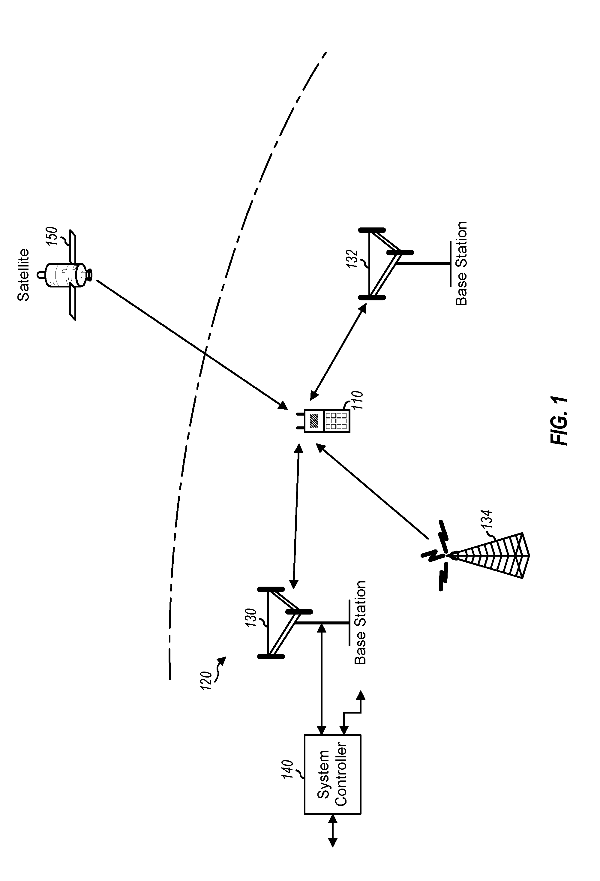
FIG. 1 shows a wireless device 110 communicating with a wireless communication system 120. Wireless system 120 may be a long term evolution (LTE) system, a code division multiple access (CDMA) system, a global system for mobile communications (GSM) system, a wireless local area network (WLAN) system, or some other wireless system. A CDMA system may implement wideband CDMA (WCDMA), time division synchronous CDMA (TD-SCDMA), CDMA2000, or some other version of CDMA. For simplicity, FIG. 1 shows wireless system 120 including two base stations 130 and 132 and one system controller 140. In general, a wireless system may include any number of base stations and any number of network entities.
Wireless device 110 may also be referred to as a user equipment (UE), a mobile station, a terminal, an access terminal, a subscriber unit, a station, etc. Wireless device 110 may be a cellular phone, a smartphone, a tablet, a wireless modem, a personal digital assistant (PDA), a handheld device, a laptop computer, a smartbook, a netbook, a cordless phone, a wireless local loop (WLL) station, a Bluetooth device, etc. Wireless device 110 may be capable of communicating with wireless system 120. Wireless device 110 may also be capable of receiving signals from broadcast stations (e.g., a broadcast station 134), signals from satellites (e.g., a satellite 150) in one or more global navigation satellite systems (GNSS), etc. Wireless device 110 may support one or more radio technologies for wireless communication such as LTE, CDMA2000, WCDMA, TD-SCDMA, GSM, 802.11, etc.
Wireless device 110 may support carrier aggregation, which is operation on multiple carriers. Carrier aggregation may also be referred to as multi-carrier operation. According to an aspect of the present disclosure, wireless device 110 may be able to operate in low-band from 698 to 960 megahertz (MHz), mid-band from 1475 to 2170 MHz, and/or high-band from 2300 to 2690, ultra-high band from 3400 to 3800 MHz, and long-term evolution (LTE) in LTE unlicensed bands (LTE-U/LAA) from 5150 MHz to 5950 MHz. Low-band, mid-band, high-band, ultra-high band, and LTE-U refer to five groups of bands (or band groups), with each band group including a number of frequency bands (or simply, "bands"). For example, in some systems each band may cover up to 200 MHz and may include one or more carriers. For example, each carrier may cover up to 40 MHz in LTE. Of course, the range for each of the bands is merely exemplary and not limiting, and other frequency ranges may be used. LTE Release 11 supports 35 bands, which are referred to as LTE/UMTS bands and are listed in 3GPP TS 36.101. Wireless device 110 may be configured with up to 5 carriers in one or two bands in LTE Release 11.
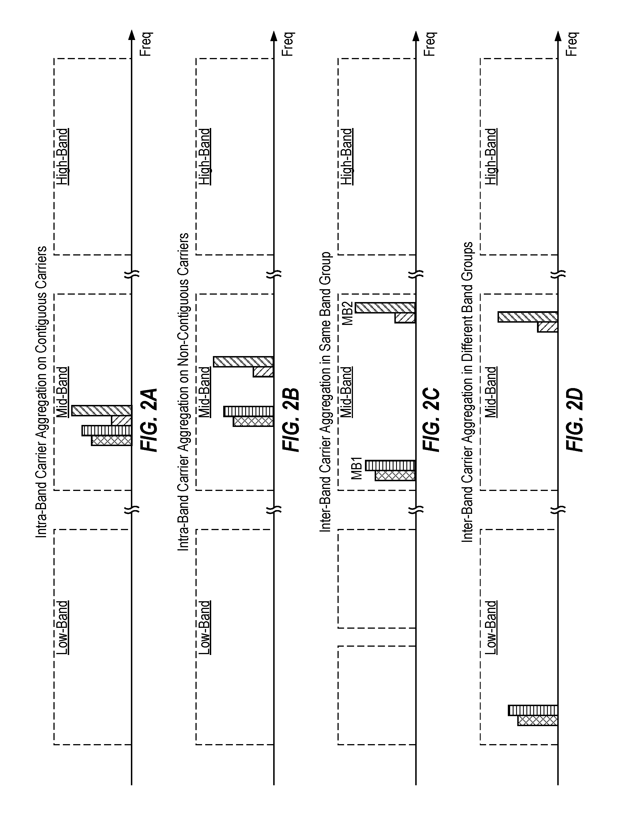
In general, carrier aggregation (CA) may be categorized into two types: intra-band CA and inter-band CA. Intra-band CA refers to operation on multiple carriers within the same band and inter-band CA refers to operation on multiple carriers in different bands.
FIG. 2A shows an example of contiguous intra-band CA. In the example shown in FIG. 2A, a wireless device (e.g., wireless device 110) is configured with four contiguous carriers in the same band, which is a band in mid-band. The wireless device may send and/or receive transmissions on multiple contiguous carriers within the same band.
FIG. 2B shows an example of non-contiguous intra-band CA. In the example shown in FIG. 2B, a wireless device (e.g., wireless device 110) is configured with four non-contiguous carriers in the same band, which is a band in mid-band. The carriers may be separated by 5 MHz, 10 MHz, or some other amount. The wireless device may send and/or receive transmissions on multiple non-contiguous carriers within the same band.
FIG. 2C shows an example of inter-band CA in the same band group. In the example shown in FIG. 2C, a wireless device (e.g., wireless device 110) is configured with four carriers in two bands in the same band group, which is mid-band. The wireless device may send and/or receive transmissions on multiple carriers in different bands in the same band group (e.g., Mid-Band 1 (MB1) and Mid-Band 2 (MB2) in FIG. 2C).
FIG. 2D shows an example of inter-band CA in different band groups. In the example shown in FIG. 2D, a wireless device (e.g., wireless device 110) is configured with four carriers in two bands in different band groups, which include two carriers in one band in low-band and two additional carriers in another band in mid-band. The wireless device may send and/or receive transmissions on multiple carriers in different bands in different band groups (e.g., low-band and mid-band in FIG. 2D). FIGS. 2A to 2D show four examples of carrier aggregation. Carrier aggregation may also be supported for other combinations of bands and band groups. For example, carrier aggregation may be supported for low-band and high-band, mid-band and high-band, high-band and high-band, and other band combinations with ultra-high band and long-term evolution in unlicenced spectrum (LTE-U).
FIG. 3 shows a block diagram of an exemplary design of wireless device 110 in FIG. 1. In this exemplary design, wireless device 110 includes a transceiver 320 coupled to a primary antenna 310, receivers 322 coupled to a secondary antenna 312, and a data processor/controller 380. Transceiver 320 includes multiple (K) receivers 330aa to 330ak and multiple (K) transmitters 360a to 360k to support multiple bands, carrier aggregation, multiple radio technologies, etc. Receivers 322 include multiple (M) receivers 330ba to 330bm to support multiple bands, carrier aggregation, multiple radio technologies, receive diversity, MIMO transmission from multiple transmit antennas to multiple receive antennas, etc.
In the exemplary design shown in FIG. 3, each receiver 330 includes input circuits 332, a low-noise amplifier (LNA) 340, and receive circuits 342. For data reception, antenna 310 receives signals from base stations and/or other transmitter stations and provides a received RF signal, which is routed through an antenna interface circuit 324 and provided to a selected receiver. Antenna interface circuit 324 may include switches, duplexers, transmit filters, receive filters, etc. The description below assumes that receiver 330aa is the selected receiver. Within receiver 330aa, the received RF signal is passed through input circuits 332aa, which provides an input RF signal to an LNA 340aa. Input circuits 332aa may include a matching circuit, a receive filter, etc. LNA 340aa amplifies the input RF signal and provides an output RF signal. Receive circuits 342aa amplify, filter, and downconvert the output RF signal from RF to baseband and provide an analog input signal to data processor 380. Receive circuits 332 aa may include mixers, filters, amplifiers, matching circuits, an oscillator, a local oscillator (LO) generator, a phase locked loop (PLL), etc. Each remaining receiver 330 in transceiver 320 and each receiver 330 in receivers 322 may operate in similar manner as receiver 330aa in transceiver 320.
In the exemplary design shown in FIG. 3, each transmitter 360 includes transmit circuits 362, a power amplifier (PA) 364, and output circuits 366. For data transmission, data processor 380 processes (e.g., encodes and modulates) data to be transmitted and provides an analog output signal to a selected transmitter. The description below assumes that transmitter 360a is the selected transmitter. Within transmitter 360a, transmit circuits 362a amplify, filter, and upconvert the analog output signal from baseband to RF and provide a modulated RF signal. Transmit circuits 362a may include amplifiers, filters, mixers, matching circuits, an oscillator, an LO generator, a PLL, etc. A PA 364a receives and amplifies the modulated RF signal and provides a transmit RF signal having the proper output power level. The transmit RF signal is passed through output circuits 366a, routed through antenna interface circuit 324, and transmitted via antenna 310. Output circuits 366a may include a matching circuit, a transmit filter, a directional coupler, etc.
FIG. 3 shows an exemplary design of receivers 330 and transmitters 360. A receiver and a transmitter may also include other circuits not shown in FIG. 3, such as filters, matching circuits, etc. All or a portion of transceiver 320 and receivers 322 may be implemented on one or more analog integrated circuits (ICs), RF ICs (RFICs), mixed-signal ICs, etc. For example, LNAs 340, receive circuits 342, and transmit circuits 362 may be implemented on one module, which may be an RFIC, etc. Antenna interface circuits 324 and 326, input circuits 332, output circuits 366, and PAs 364 may be implemented on another module, which may be a hybrid module, etc. The circuits in transceiver 320 and receivers 322 may also be implemented in other manners.
Data processor/controller 380 may perform various functions for wireless device 110. For example, data processor 380 may perform processing for data being received via receivers 330 and data being transmitted via transmitters 360. Controller 380 may control the operation of antenna interface circuits 324 and 326, input circuits 332, LNAs 340, receive circuits 342, transmit circuits 362, PAs 364, output circuits 366, or a combination thereof. A memory 382 may store program codes and data for data processor/controller 380. Data processor/controller 380 may be implemented on one or more application specific integrated circuits (ASICs) and/or other ICs.
Wireless device 110 may receive transmissions from one or more base stations/cells on multiple carriers at different frequencies for carrier aggregation. For intra-band CA, the transmissions are sent on different carriers in the same band. For inter-band CA, the transmissions are sent on multiple carriers in different bands.
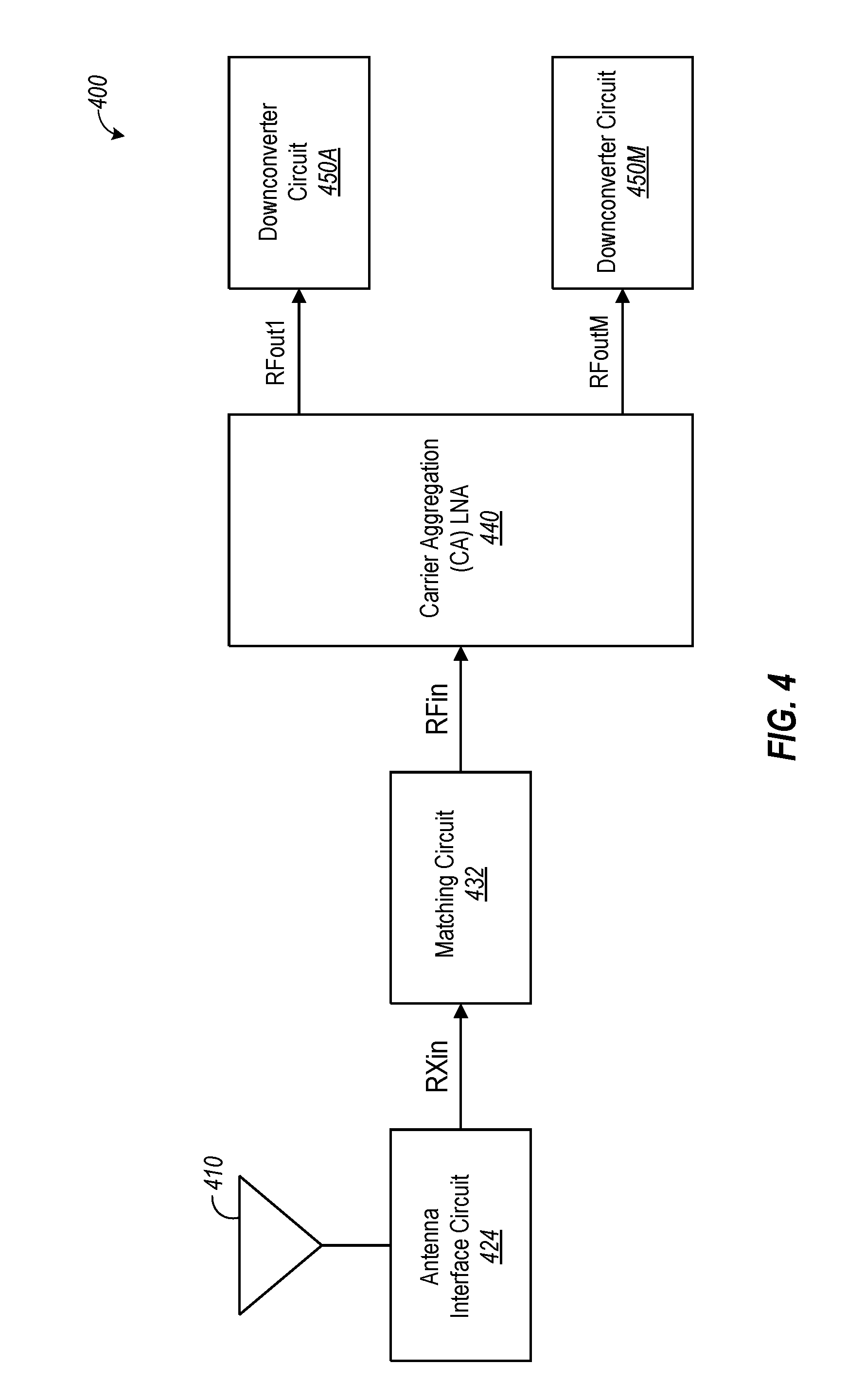
FIG. 4 shows a block diagram of an exemplary design of a receiver 400 with a carrier aggregation (CA) low-noise amplifier (LNA) 440 configured to support intra-band or inter-band CA. CA LNA 440 may be used for one or more LNAs 340 shown in FIG. 3. CA LNA 440 includes single input and multiple (M) outputs, where M>1.
At receiver 400, an antenna 410 may receive downlink signals comprising one or more transmissions sent on one or more carriers and provide a received RF signal to an antenna interface circuit 424. Antenna interface circuit 424 may filter and route the received RF signal and provide a receiver input signal, RXin. An input matching circuit 432 may receive the RXin signal and provide an input RF signal, RFin, to CA LNA 440. Matching circuit 432 may perform impedance and/or power matching between CA LNA 440 and either antenna interface circuit 424 or antenna 410 for a band of interest. Matching circuit 432 may be part of one of input circuits 332 in FIG. 3.
CA LNA 440 may receive and amplify the input RFin signal and provide (i) one output RF signal via one LNA output for either no CA or CA on one set of carriers or (ii) up to M output RF signals, RFout1 to RFoutM, via up to M LNA outputs for intra-band CA on up to M sets of carriers. In some aspects, receiver 400 may comprise a wideband LNA with a bandwidth defined to accommodate or facilitate inter-band CA using an LNA. For example, CA LNA 440 may receive multiple inputs and generates multiple outputs to support inter-band carrier aggregation within one LNA, which utilizes wide matching bandwidth and also limits the isolation between inter-band carriers. M downconverter circuits 450A to 450M are coupled to the M LNA outputs. Each downconverter circuit 450, when enabled, may downconvert an associated output RF signal such that one or more transmissions on one or more carriers of interest are downconverted from RF to baseband.
A CA LNA, such as CA LNA 440 in FIG. 4, may operate in a single-output mode or a multi-output mode at any given moment. In the single-output mode, the CA LNA operates in a 1-input to 1-output (1.times.1) configuration, and receives one input RF signal comprising one or more transmissions on one set of carriers, and provides one output RF signal to one downconverter circuit. The single-output mode may be used to receive a transmission sent on a single carrier without carrier aggregation. The single-output mode may also be used to receive transmissions sent on multiple carriers (e.g., contiguous carriers) with carrier aggregation. In this case, the transmissions on all carriers may be downconverted with a single local oscillator (LO) signal at a single frequency. In the multi-output mode, the CA LNA operates in a 1.times.M configuration, receives one input RF signal comprising multiple transmissions on M sets of carriers, and provides M output RF signals to M downconverter circuits, one output RF signal for each set of carriers, where M>1. Each set of carriers may include one or more carriers in a single band (e.g., intra-band CA) or across multiple bands (e.g., inter-band CA).
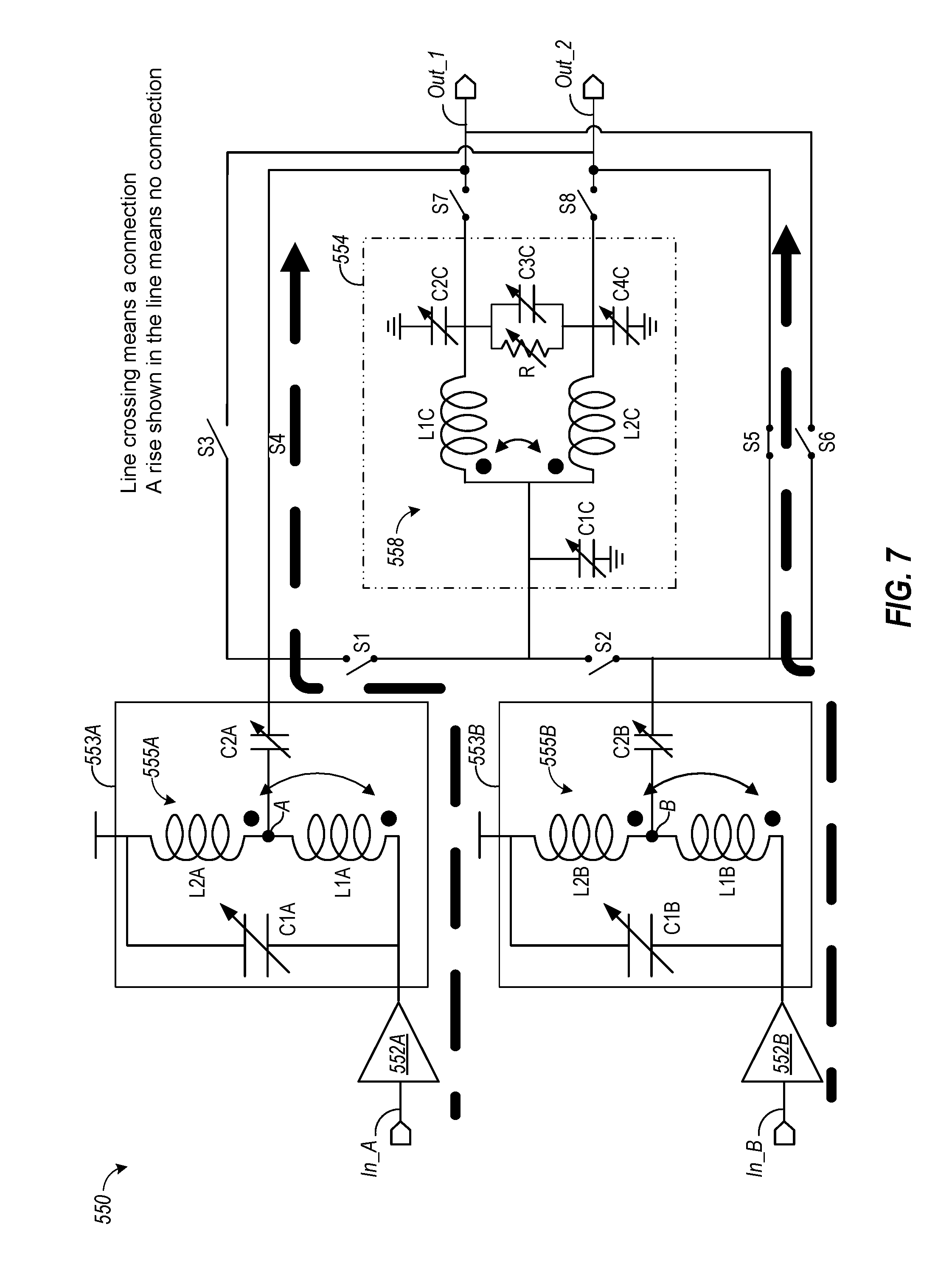
FIG. 5 depicts a device 550, according to an exemplary aspect of the present disclosure. Device 550 includes a first LNA 552A including an input In_A and an output, which is coupled to the output load and matching circuit 553A. Matching circuit 553A includes a variable capacitor C1A (e.g., multiple sections, butterfly, split stator, or differential) and a transformer 555A including an inductor L1A and an inductor L2A. Of course, other configurations of the matching circuit are also are possible. For example, in some aspects, Matching circuit 553A may be configured using resistors for matching, by removing a capacitor (e.g., C1A), or using other equivalent circuits thereof for matching circuit 553A. In some aspects, the device 550 may perform matching without a transformer, without a capacitor, or can use a resistor, or other equivalent circuits. Matching circuit 553A may further include a variable capacitor C2A coupled to a node A between inductors L1A and L2A. Device 550 may also include a second LNA 552B including an input In_B and an output, which is coupled to a matching circuit 553B. Matching circuit 553B may further include a variable capacitor C1B and a transformer 555B, which includes inductor L1B and an inductor L2B. Matching circuit 553B further includes a variable capacitor C2B coupled to a node B between inductor L1B and L2B. It is noted that LNA 552B and matching circuit 553B may be used in conjunction with LNA 552A and matching circuit 553A, and share a power splitter 554, to operate in an inter-band or intra-band mode, as will be appreciated by a person having ordinary skill in the art.
Power splitter 554 may include a variable capacitor C1C, a transformer 558, variable capacitors C2C, C3C, and C4C, and a variable resistor R1C. As will be appreciated, by tuning variable resistor RC1, one or more of variable capacitors C1C, C2C, C3C, and C4C, or any combination thereof, isolation between signals at outputs Out_1 and Out_2 of power splitter 554 may be varied. As one example, provided without limitation, in one tuner setting, the isolation at approximately 2.6 GHz may be approximately -46.58 dB. Various other tuner settings having a variety of other isolations can also be achieved. In related aspects, there can be more than two outputs to account for when CA is greater than two.
Transformer 558 may comprise, without limitation, a quarter-wave transformer, a triple-coil transformers, etc. Transformer 558 may include an inductor L1C and an inductor L2C. Device 550 may further include a plurality of switches S1-S8, and outputs Out_1 and Out_2. Outputs Out_1 and Out_2 may be configured to couple to another device. For example, each of output Out_1 and output Out_2 may couple to downconversion circuitry. Using the power splitter 554 is beneficial because it offers good signal isolation and linearity.
The variable capacitors C1C, C2C, C3C, and C4C may be implemented as switched capacitors, where switches and different sizes of capacitors are connected in an array. In related aspects, fixed capacitors may be used if the specified signal bandwidth is limited to some particular band. In additional related aspects, variable capacitors may be used, where the capacitor value can be continuously tuned with voltages. The variable resistor R1C may be implemented as a switched resistor, where switches and different sizes of resistors are connected in an array.
Device 550 also includes the reconfigurable switches S1-S8. S3 and S4 are switches connected to an output matching circuit 553A, so that the LNA 552A can conduct an output signal to output ports Out_1 and Out_2 directly. S5 and S6 are switches connected to an output of matching circuit 553B, so that the LNA 552B can conduct an output signal to output ports Out_1 and Out_2 directly. S1 and S2 are connected to the LNA 552A and LNA 552B, respectively, and conduct the output signal of either LNA 552A or LNA 552B so that it can go through power splitter 554, where the signal is split into two output paths that travel through switches S7 and S8, and then to the two output ports Out_1 and Out_2.
By combining these output switches S1-S8 with tunable power splitter 554, LNA 552 can generate multiple outputs together with tunable isolations. Power splitter 554 will also match to the output impedance without the need to add extra matching networks.
In addition, device 550 may include, or may be in communication with, a controller 560 configured for controlling operation of one or more components of one or more matching circuits (e.g., 553A, 553B) and power splitter 554. As one example, controller 560 may generate and convey one or more control signals CNT to vary one or more variable capacitors of device 550, variable resistor R1C of device 550, one or more transformers of device 550, or any combination thereof. Additionally, opening and closing of switches S1-S8 may be controlled by controller 560 in order to determine whether one or both matching circuit 553 is coupled to power splitter 554. For example, control signal CNT can be used for controlling switches S1-S8.
FIG. 6 depicts LNA 552, which may comprise LNA 552A and LNA 552B of FIG. 5. LNA 552 includes an input LNA_IN, an inductor L1, an electrostatic discharge (ESD) protection device 562, a DC blocking capacitor C1, bias filtering capacitors C2, C4, and C5, and a capacitor C3, which may comprise a variable capacitor. LNA 552 further includes an inductor L2, a main transistor M1, a three cascade transistor comprising M2, M3, and M4, and an output LNA_OUT.
As illustrated in FIG. 6, transistor M1 amplifies the signal from LNA_IN and generates a current to feed through the source of cascode transistors M2 and M3. Cascode transistors M2, M3 and M4 can behave as two branches. One branch can be a single cascode branch comprising M2, while the other branch can be a double cascode branch comprising M3 and M4. The drains of M2 and M4 are connected together so that the current of both branches can be combined. The single cascode branch and double cascode branch can be controlled to be either in an on or off state so that the gain of the LNA 552 can be changed according to the operation mode.
The gate of transistor M1 is coupled to capacitor C1, which is further coupled to inductor L1. Inductor L1 can also be coupled to input LNA_IN. Inductor L2 is coupled between transistor M1 (e.g., a source of transistor M1) and a ground voltage GRND, transistor M2 is coupled to transistor M1, and transistor M2 is coupled to output LNA_OUT. Moreover, a gate of transistor M1 is coupled to a source of transistor M1 via capacitor C3. In some aspects, capacitor C3 may be implemented as a switched capacitor array, so that the input impedance of LNA 552 could be tuned and optimized with different source impedance. The NF and linearity may also be improved with different settings of capacitor C3.
In addition, LNA 552 may include, or may be in communication with, a bias block 570 configured for generating a bias voltage for M1, M2, M3, and M4, corresponding to bias voltages VB_MAIN, VB_CASC1, VB_CASC2 and VB_CASC3. Different bias voltages can be generated according to the gain, noise figure and linearity requirement of LNA. The bias block 570 will generate the bias voltage for M1, M2, M3, and M4 so that only one of the single cascode branch and double cascode branch can be turned on at a given time, so that the noise contribution of M2, M3 and M4 to the LNA output LNA_OUT can be improved.
The benefit of implementing a single cascode branch and a double cascode branch is to improve the gain since the output impedance of the double cascode branch is higher than the single cascode branch, and the input-output isolation of the double cascode branch is also improved. However, a single cascode branch can offer better linearity and larger output swing within a given supply voltage.
FIG. 7 illustrates an exemplary operation of device 550 in accordance with aspects of the present disclosure. More specifically, FIG. 7 illustrates device 550 operating in legacy/inter-CA mode or intra-CA mode, wherein power splitter 554 is bypassed (shown by the dashed line along the alternate paths between IN_A and Out_1 and IN_B and Out 2). More specifically, in this contemplated operation, switches S1 and S2 may be open and switches S3 and S4 may be closed. Thus, the output of matching circuit 553A is coupled to at least one of output Out_1 and output Out_2. Alternatively, at least one of switches S3 or S4 may be closed to couple one of output Out_1 or Out_2 to matching circuit 553A. Similarly, at least one of switches S5 or S6 may be closed to couple at least one of outputs Out_1 or Out_2 to matching circuit 553B. For example, as shown in FIG. 7, LNA 552A can be coupled to Out_1 and LNA 552B can be coupled to Out_2 by opening switches S1, S2, S3, and S6, and closing switches S4 and S5. By controlling switches S1-S6, device 550 can be dynamically controlled to function in various inter-band CA or intra-band CA configurations. In an aspect, values of NF, linearity, and power consumption may be improved without introducing excessive parasitic values at the input of device 550.
FIG. 8 illustrates another exemplary operation of device 550 in accordance with aspects of the present disclosure. More specifically, FIG. 8 illustrates an example of device 550 operating in an intra-CA mode (shown by way of multiple output paths). In this contemplated operation, a signal may be conveyed from matching circuit 553A to power splitter 554 via switch S1, which may be in a closed configuration. Further, in this aspect, switches S4 and S3 may be in an open configuration. During this contemplated operation, power splitter 554 may split an input signal into two equal phase output signals. Power splitter 554 may utilize one or more quarter-wave transformers to match output ports to an input port. Because a loss-less reciprocal three-port network cannot have all ports simultaneously matched, one resistor R may be added between the two output ports. In addition to matching all three ports, resistor R may isolate the two output ports from one another at the center frequency. Further, the resistor R may not add resistive loss from the input port to output ports.
By opening switch S1 and closing switch S2, while leaving switches S3-S6 open, LNA 552B can be coupled to power splitter 554 so that the LNA 552B can operate in intra-CA mode, for example. The sharing of power splitter 554 between LNA 552A and LNA 552B reduces the chip area and thus reduces the chip cost.
In one exemplary aspect, power splitter 554 can comprise a Wilkinson power splitter. The Wilkinson power splitter is a well-known device in the RF/microwave community used for splitting or combining signals. A conventional Wilkinson power splitter is composed of simple transmission lines and a resistor, and takes advantage of the properties of quarter wavelength transmission line sections to provide ideal power divider characteristics. According to aspects of the present disclosure, the power splitter 554 may be an on chip transformer, offering high level of isolation tenability and aggressive area reduction.
According to aspects of the present disclosure, the power splitter 554 splits the signal equal-amplitude, equal-phase output signals from the splitter input to the splitter output (Out_1 and Out_2) with some switch losses. L1C, C2C and half of C1C are implemented as a quarter-wave length transmission line in the desired frequency. By deriving the terminal impedance at the input, the terminated impedances at output ports Out_1 and Out_2 will be converted through the quarter-wave length transmission line and then combined together at the input. For example, the quarter-wave length transmission line characteristic impedance can be set, without limitation, to 1.414.times.Z0, so that the input is matched when ports 2 and 3 are terminated in Z0.
In one example, the isolation of power splitters 554 may be at least 6 dB better than the return loss of the source match at input port In_A. A return loss of power splitter 554 may be no better than a return loss observed by power splitters 554 at input port In_A.
The resistor R and the capacitor C3C are implemented as 2.times.Z0 between the two outputs. R could also be tuned with different Z0 impedances, or tuned if the process and/or temperature changes. Because each end of an isolation resistor R between output ports Out_1 and Out_2 is at the same potential, no current flows through the resistor R, and therefore the resistor R is decoupled from input port In_A.
One or more of capacitors C1C/C2C/C3C/C4C may be used to tune a center frequency under different CA operations. One or more of capacitors C1C/C2C/C3C/C4C may also be used to tune the center frequency when the process and/or temperature changes.
It is noted that power splitter 554 may be configured with improved insertion loss and CA isolation. It is further noted that there may be a small NF difference at intra-CA mode because the signal is splitting at outputs Out_1 and Out_2. Further, gain degradation can be compensated back with current bias or programmable degeneration. Compared to other CA LNA topologies, CA isolation may be tuned independently without reducing the NF/linearity performance. For example, one or more of capacitors C1C/C2C/C3C/C4C and resistor R can be used to tune power splitter 554 independently of LNA 552.
It is further noted that in each of the aspects shown in FIGS. 5 and 6, LNA 552B is not receiving a signal and, therefore, neither LNA 552B nor matching circuit 553B may contribute to an output (e.g., at outputs Out_1 and Out_2). However, as noted above, in one exemplary aspect, LNA 552B and matching circuit 553B may be used in conjunction with LNA 552A and matching circuit 553A, and power splitter 554 may be shared (e.g., receive a signal from matching circuit 553A and a signal from matching circuit 553B), to operate in an inter-band mode, as will be appreciated by a person having ordinary skill in the art. For example, switches S1 and S2 may be closed, and switches S3-S6 may be opened, to allow input signals In_A and In_B to pass through to power splitter 554. In related aspects, switches S1 and S2 may be closed simultaneously, or alternated to close at alternating times, while switches S3-S6 remain open, to keep signals In_A and In_B separated.
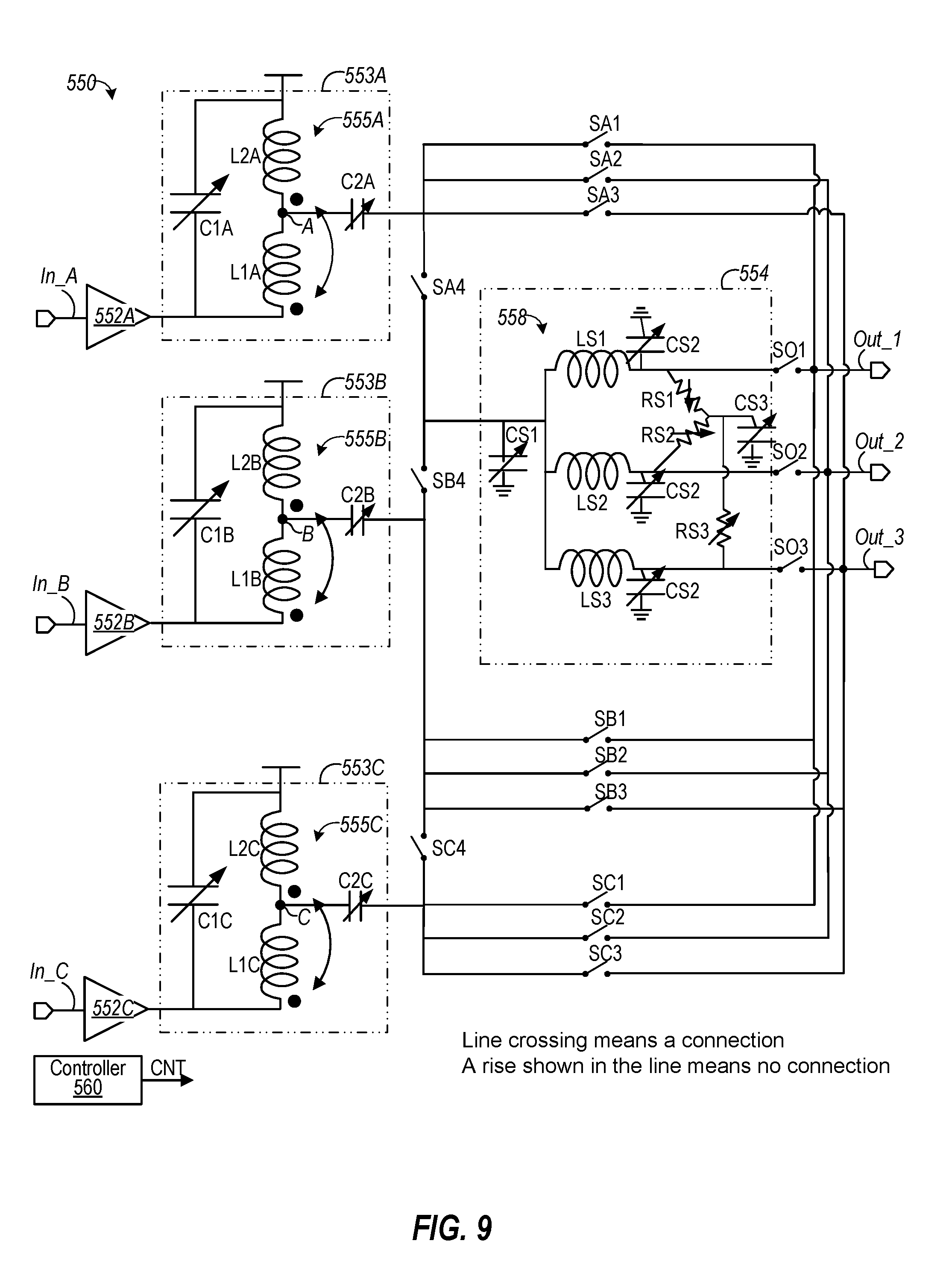
FIG. 9 illustrates a device 550 including a low-noise amplifier with a tunable integrated power splitter, supporting three contiguous intra-band carrier aggregation (CA), according to an aspect of the present disclosure.
In FIG. 9, device 550 includes three LNA devices, 552A, 552B and 552C, all implemented as shown in FIG. 6. Each LNA device 552A, 552B and 552C is connected to the output loading and matching circuits 553A, 553B, and 553C. By configuring the switches SA1-SA3, SB1-SB3 and SC1-SC3 accordingly, the three LNAs 552A, 552B and 552C can be configured for inter-band CA mode, where the three input signals at the input nodes, In_A, In_B, and In_C, can be amplified and coupled to Out_1, Out_2, and Out_3, respectively. Each LNA 552A, 552B and 552C can connect to either Out_1, Out_2, or Out_3 such that different downlink paths can be utilized.
In addition, device 550 has a power splitter 554 (e.g., a single-input-triple-output splitter) for supporting three contiguous intra-band CA. Power splitter 554 includes a transformer including three inductors (e.g., inductor coils) LS1, LS2, and LS3, and tunable capacitors CS1, CS2, and CS3. Three resistors RS1, RS2, and RS3 are added across the splitter output to tune the impedance, so that the isolation between Out_1, Out_2, and Out_3 can be improved. Similar to device 550 in FIG. 5, the power splitter 554 splits the signal with equal-amplitude and equal-phase to output signals from the splitter input to the splitter output (Out_1, Out_2 and Out_3) with some switch losses. LS1, CS2 and one third of CS1, are implemented as a quarter-wave length transmission line in the desired frequency. The characteristic impedance of the quarter-wave lines can be equal, without limitation, to 1.732.times.Z0, and the resistors RS1, RS2, and RS3 can be implemented, without limitation, as 3.times.Z0 between the two outputs.
One or more of capacitors CS1/CS2/CS3 may be used to tune a center frequency under different CA operations. One or more of capacitors CS1/CS2/CS3 and resistors RS1/RS2/RS3 may also be used to tune the center frequency when the process and/or temperature changes.
FIG. 10 illustrates a device 550 including a low-noise amplifier (LNA) 552 with tunable integrated power splitter 554, with an alternative matching circuit 553 between LNA output and splitter input, according to another aspect of the present disclosure.
In FIG. 10, L1A and L2A are implemented in such a way that C2A and C2B (see FIG. 9) are removed in FIG. 10. L2A is connected between a power source (e.g., a VDD) and an output of LNA 552A, while L1A couples the signal from L2A and feeds the signal to power splitter 554 input through switches S1. The other side of L1A is coupled to the ground. The coupling co-efficient and inductance value can be designed to implement appropriate voltage gain at the output of LNA 552A and appropriate impedance translation from the output of LNA 552A.
Because C2A and C2B are removed, additional space is saved on the device 550. The outputs of transformers L1A and L1B can also be DC coupled to switches S1-S6.
FIG. 11 shows an exemplary controller 1100 for use with device 550 shown in FIGS. 5-8. For example, controller 1100 is suitable for use as the controller 380 shown in FIG. 3 and/or controller 560 shown in FIG. 5. Controller 1100 comprises processor 1102, memory 1104, switch controller 1106, and component controller 1108. Processor 1102, memory 1104, switch controller 1106, and component controller 1108 may all be electrically coupled to communication bus 1110 to communicate with each other.
Processor 1102 comprises a CPU, processor, gate array, hardware logic, discrete circuits, memory elements, and/or hardware executing software. Processor 1102 operates to control the other functional elements of controller 1100 using communication bus 1110. Processor 1102 can execute instructions stored in memory 1104 or operate in accordance with instructions, commands, data, or other information received over a processor control line 1112. In an exemplary aspect, another entity (not shown) at the device generates the information on processor control line 1112.
Memory 1104 comprises any suitable memory or storage device that allows for storing, retrieving, and maintaining instructions and/or data associated with the operation of controller 1100. In an exemplary aspect, memory 1104 stores algorithm instructions that can be executed by processor 1102 to perform the functions of the dual stage LNA as described herein.
Switch controller 1106 may be a single unit or in some aspects, may be distributed over multiple units. Switch controller 1106 may, for example, comprise hardware, such as amplifiers, buffers, registers, gates, transistors, analog to digital converters, digital to analog converters or any other suitable hardware or discrete components and/or hardware executing software that operates to output control signals to the switches used in the various exemplary aspects described above. In one exemplary aspect, processor 1102 may operate to determine switch settings for one or more of the switches used in the various aspects and pass these switch settings to switch controller 1106. Switch controller 1106 may output one or more control signals to the designated switches to adjust their switch settings according to the determinations made by processor 1102. In an exemplary aspect, processor 1102 determines that the switch settings of switches S1-S6 (see e.g., FIG. 5) are to be changed to new switch settings. Processor 1102 sends the new switch settings to switch controller 1106, which outputs the one or more control signals to switches S1-S6 for the new switch settings. In an exemplary aspect, switch controller 1106 is configured to output analog and/or digital control signals as necessary.
Component controller 1108 may be a single unit or may be distributed over multiple units, and may for instance, comprise hardware, such as amplifiers, buffers, registers, gates, transistors, analog-to-digital converters, digital to analog converters or any other suitable hardware or discrete components and/or hardware executing software that may operate to output control signals to tune the operation of variable resistors, variable capacitors, and transformers (e.g., a triple-coil transformer) of device 550 (see e.g., FIG. 5). For example, processor 1102 may operate to determine operating parameters (e.g., frequency tunings) for each of the transformer circuits and variable components (e.g., variable capacitors and variable resistors) and passes these adjustments to component controller 1108. More specifically, for example, component controller 1108 may output signals to tune one or more components of power splitter 554 (see e.g., FIG. 5). Component controller 1108 outputs control signals to adjust the operation of the device 550 according to the determinations made by processor 1102.
It should be noted that controller 1100 represents just one implementation and that other implementations are possible. For example, controller 1100 may be implemented in discrete logic that eliminates the need for a processor or memory devices. In another implementation, the functions and/or implementations of controller 1100 are incorporated or integrated into a baseband processor or other entity at the receiving device.
According to another exemplary aspect, the present disclosure includes methods for operating a wireless receiver. Various aspects of such a method may include amplifying a signal with a low-noise amplifier (LNA). The method may further include configuring at least one switch to either convey the amplified signal to at least one output or convey the amplified signal to the at least one output via a power splitter.
FIG. 12 is a flowchart illustrating a method 1200, in accordance with aspects of the present disclosure. Method 1200 may amplify a signal with a low-noise amplifier (LNA) (block 1202). Method 1200 may also include configuring at least one switch to either convey the amplified signal to one or more outputs or convey the amplified signal to the one or more outputs via a power splitter (block 1204).
FIG. 13 shows an exemplary amplifier device 1300 in accordance with aspects of the present disclosure. For example, device 1300 is suitable for use as device 550 of FIG. 5. In an aspect, device 1300 is implemented by one or more modules configured to provide the functions as described herein. For example, in an aspect, each module comprises hardware and/or hardware executing software.
Device 1300 comprises a first module comprising means (1302) for amplifying a signal with a low-noise amplifier (LNA). For example, means 1302 may comprise LNA 552A of FIG. 5.
Device 1300 also comprises a second module comprising means (1304) for configuring at least one switch to either convey the amplified signal to one or more outputs or convey the amplified signal to the one or more outputs via a power splitter For example, means 1304 may include controller 560 of FIG. 5.
Those of skill in the art would understand that information and signals may be represented using any of a variety of different technologies and techniques. For example, data, instructions, commands, information, signals, bits, symbols, and chips that may be referenced throughout the above description may be represented by voltages, currents, electromagnetic waves, magnetic fields or particles, optical fields or particles, or any combination thereof.
Those of skill would further appreciate that the various illustrative logical blocks, modules, circuits, and algorithm steps described in connection with the exemplary embodiments disclosed herein may be implemented as electronic hardware, computer software, or combinations of both. To clearly illustrate this interchangeability of hardware and software, various illustrative components, blocks, modules, circuits, and steps have been described above generally in terms of their functionality. Whether such functionality is implemented as hardware or software depends upon the particular application and design constraints imposed on the overall system. Skilled artisans may implement the described functionality in varying ways for each particular application, but such implementation decisions should not be interpreted as causing a departure from the scope of the exemplary embodiments.
The various illustrative logical blocks, modules, and circuits described in connection with the exemplary embodiments disclosed herein may be implemented or performed with a general purpose processor, a Digital Signal Processor (DSP), an Application Specific Integrated Circuit (ASIC), a Field Programmable Gate Array (FPGA) or other programmable logic device, discrete gate or transistor logic, discrete hardware components, or any combination thereof designed to perform the functions described herein. A general purpose processor may be a microprocessor, but in the alternative, the processor may be any conventional processor, controller, microcontroller, or state machine. A processor may also be implemented as a combination of computing devices, e.g., a combination of a DSP and a microprocessor, a plurality of microprocessors, one or more microprocessors in conjunction with a DSP core, or any other such configuration.
In one or more exemplary aspects, the functions described may be implemented in hardware, software, firmware, or any combination thereof. If implemented in software, the functions may be stored on or transmitted over as one or more instructions or code on a computer-readable medium. Computer-readable media includes both computer storage media and communication media including any medium that facilitates transfer of a computer program from one place to another. A storage media may be any available media that can be accessed by a computer. By way of example, and not limitation, such computer-readable media can comprise RAM, ROM, EEPROM, CD-ROM or other optical disk storage, magnetic disk storage or other magnetic storage devices, or any other medium that can be used to carry or store desired program code in the form of instructions or data structures and that can be accessed by a computer. Also, any connection is properly termed a computer-readable medium. For example, if the software is transmitted from a website, server, or other remote source using a coaxial cable, fiber optic cable, twisted pair, digital subscriber line (DSL), or wireless technologies such as infrared, radio, and microwave, then the coaxial cable, fiber optic cable, twisted pair, DSL, or wireless technologies such as infrared, radio, and microwave are included in the definition of medium. Disk and disc, as used herein, includes compact disc (CD), laser disc, optical disc, digital versatile disc (DVD), floppy disk and blu-ray disc where disks usually reproduce data magnetically, while discs reproduce data optically with lasers. Combinations of the above should also be included within the scope of computer-readable media.
It is noted that combinations such as "at least one of A, B, or C," "at least one of A, B, and C," and "A, B, C, or any combination thereof" include any combination of A, B, and/or C, and may include multiples of A, multiples of B, or multiples of C. Specifically, combinations such as "at least one of A, B, or C," "at least one of A, B, and C," and "A, B, C, or any combination thereof" may be A only, B only, C only, A and B, A and C, B and C, or A and B and C, where any such combinations may contain one or more member or members of A, B, or C.
The previous description of the disclosed exemplary aspects is provided to enable any person skilled in the art to make or use the present disclosure. Various modifications to these exemplary aspects will be readily apparent to those skilled in the art, and the generic principles defined herein may be applied to other aspects without departing from the spirit or scope of the disclosure. Thus, the present disclosure is not intended to be limited to the exemplary aspects shown herein but is to be accorded the widest scope consistent with the principles and novel features disclosed herein.
* * * * *
D00000
D00001
D00002
D00003
D00004
D00005
D00006
D00007
D00008
D00009
D00010
D00011
D00012
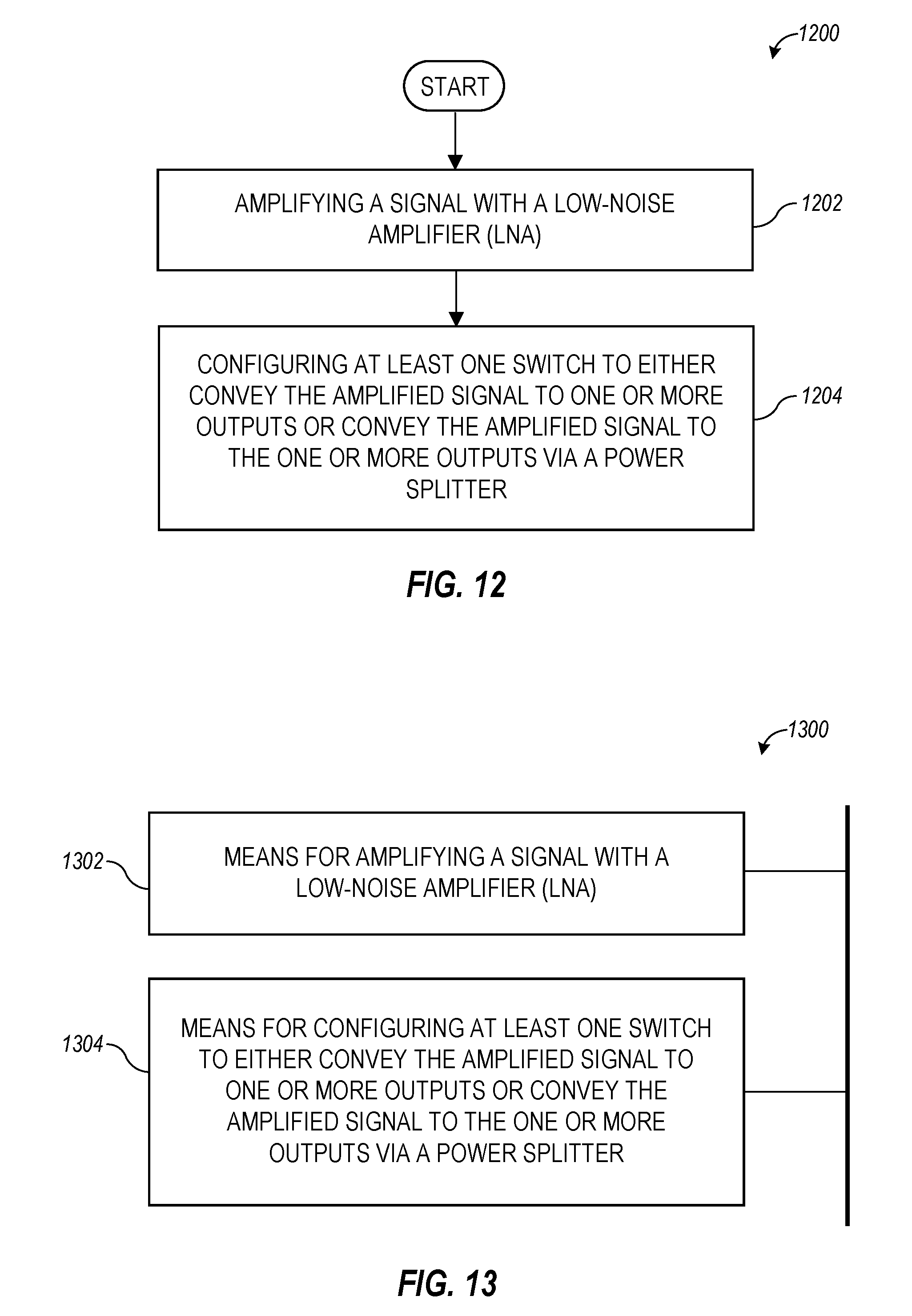
XML
uspto.report is an independent third-party trademark research tool that is not affiliated, endorsed, or sponsored by the United States Patent and Trademark Office (USPTO) or any other governmental organization. The information provided by uspto.report is based on publicly available data at the time of writing and is intended for informational purposes only.
While we strive to provide accurate and up-to-date information, we do not guarantee the accuracy, completeness, reliability, or suitability of the information displayed on this site. The use of this site is at your own risk. Any reliance you place on such information is therefore strictly at your own risk.
All official trademark data, including owner information, should be verified by visiting the official USPTO website at www.uspto.gov. This site is not intended to replace professional legal advice and should not be used as a substitute for consulting with a legal professional who is knowledgeable about trademark law.