FM demodulation system for quartz MEMS magnetometer
Sorenson , et al. J
U.S. patent number 10,175,307 [Application Number 14/997,203] was granted by the patent office on 2019-01-08 for fm demodulation system for quartz mems magnetometer. This patent grant is currently assigned to HRL Laboratories, LLC. The grantee listed for this patent is HRL Laboratories, LLC. Invention is credited to David T. Chang, Joshua A. Erbland, L. X. Coco Huang, Hung Nguyen, Raviv Perahia, Logan D. Sorenson.


| United States Patent | 10,175,307 |
| Sorenson , et al. | January 8, 2019 |
FM demodulation system for quartz MEMS magnetometer
Abstract
A magnetometer system has a magnetometer, an interface circuit and an electronic demodulator, the interface circuit being coupled to sense electrodes disposed on the magnetometer and the demodulator being coupled to the interface circuit. Preferably, the magnetometer has a loop electrode which follows an outline of the shape of an active portion of the magnetometer and wherein the electronic demodulator has an output for driving the loop electrode of the magnetometer. Preferably, the magnetometer includes a quartz plate with flexural and thickness shear vibratory modes and wherein the flexural vibratory mode is driven, in use, into vibration by the electronic demodulator and wherein the thickness shear vibratory mode is driven, in use, into vibration by the interface circuit.
| Inventors: | Sorenson; Logan D. (Calabasas, CA), Nguyen; Hung (Los Angeles, CA), Perahia; Raviv (Calabasas, CA), Chang; David T. (Calabasas, CA), Huang; L. X. Coco (Tarzana, CA), Erbland; Joshua A. (Brockport, NY) | ||||||||||
|---|---|---|---|---|---|---|---|---|---|---|---|
| Applicant: |
|
||||||||||
| Assignee: | HRL Laboratories, LLC (Malibu,
CA) |
||||||||||
| Family ID: | 64872538 | ||||||||||
| Appl. No.: | 14/997,203 | ||||||||||
| Filed: | January 15, 2016 |
| Current U.S. Class: | 1/1 |
| Current CPC Class: | G01R 33/0286 (20130101); G01R 33/0041 (20130101) |
| Current International Class: | G01R 33/028 (20060101); G01R 33/00 (20060101) |
References Cited [Referenced By]
U.S. Patent Documents
| 392650 | November 1888 | Watrous |
| 2487165 | November 1949 | Miller |
| 3390287 | June 1968 | Sonderegger |
| 3766616 | October 1973 | Staudte |
| 4364016 | December 1982 | Tanski |
| 4426769 | January 1984 | Grabbe |
| 4442574 | April 1984 | Wanuga |
| 4447753 | May 1984 | Ochiai |
| 4618262 | October 1986 | Maydan |
| 4870313 | September 1989 | Hirama et al. |
| 4898031 | February 1990 | Oikawa et al. |
| 4944836 | July 1990 | Beyer et al. |
| 5203208 | April 1993 | Bernstein |
| 5226321 | July 1993 | Varnham |
| 5260596 | November 1993 | Dunn et al. |
| 5421312 | June 1995 | Dawson |
| 5445008 | August 1995 | Wachter |
| 5480747 | January 1996 | Vasudev |
| 5530408 | June 1996 | Vig et al. |
| 5552016 | September 1996 | Ghanayem |
| 5578976 | November 1996 | Yao et al. |
| 5589724 | December 1996 | Satoh et al. |
| 5604312 | February 1997 | Lutz |
| 5605490 | February 1997 | Laffey et al. |
| 5644139 | July 1997 | Allen |
| 5646346 | July 1997 | Okada |
| 5648849 | July 1997 | Canteloup |
| 5658418 | August 1997 | Coronel |
| 5665915 | September 1997 | Kobayashi |
| 5666706 | September 1997 | Tomita et al. |
| 5668057 | September 1997 | Eda et al. |
| 5719324 | February 1998 | Thundat |
| 5728936 | March 1998 | Lutz |
| 5783749 | July 1998 | Lee et al. |
| 5894090 | April 1999 | Tang et al. |
| 5905202 | May 1999 | Kubena et al. |
| 5920012 | July 1999 | Pinson |
| 5928532 | July 1999 | Koshimizu |
| 5942445 | August 1999 | Kato et al. |
| 5959206 | September 1999 | Ryrko |
| 5981392 | November 1999 | Oishi |
| 5987985 | November 1999 | Okada |
| 6009751 | January 2000 | Ljung |
| 6033852 | March 2000 | Andle |
| 6044705 | April 2000 | Neukermans |
| 6049702 | April 2000 | Tham et al. |
| 6081334 | June 2000 | Grimbergen |
| 6089088 | July 2000 | Charvet |
| 6094985 | August 2000 | Kapels et al. |
| 6114801 | September 2000 | Tanaka et al. |
| 6145380 | November 2000 | MacGugan |
| 6151964 | November 2000 | Nakajima |
| 6155115 | December 2000 | Ljung |
| 6164134 | December 2000 | Cargille |
| 6182352 | February 2001 | Deschenes |
| 6196059 | March 2001 | Koesslinger |
| 6204737 | March 2001 | Ella |
| 6207008 | March 2001 | Kijima |
| 6236145 | May 2001 | Biernacki |
| 6250157 | June 2001 | Touge |
| 6263552 | July 2001 | Takeuchi |
| 6282958 | September 2001 | Fell et al. |
| 6289733 | September 2001 | Challoner |
| 6297064 | October 2001 | Koshimizu |
| 6335667 | January 2002 | Takagi |
| 6336366 | January 2002 | Thundat |
| 6349597 | February 2002 | Folkmer |
| 6367326 | April 2002 | Okada |
| 6367786 | April 2002 | Gutierrez |
| 6413682 | July 2002 | Shibano |
| 6417925 | July 2002 | Naya |
| 6424418 | July 2002 | Kawabata |
| 6426296 | July 2002 | Okojie |
| 6429652 | August 2002 | Allen |
| 6432824 | August 2002 | Yanagisawa |
| 6481284 | November 2002 | Geen et al. |
| 6481285 | November 2002 | Shkel et al. |
| 6492195 | December 2002 | Nakanishi |
| 6513380 | February 2003 | Reeds et al. |
| 6514767 | February 2003 | Natan |
| 6515278 | February 2003 | Wine et al. |
| 6571629 | June 2003 | Kipp |
| 6584845 | July 2003 | Gutierrez |
| 6614529 | September 2003 | Tang |
| 6621158 | September 2003 | Martin et al. |
| 6627067 | September 2003 | Branton |
| 6628177 | September 2003 | Clark et al. |
| 6629460 | October 2003 | Challoner |
| 6651027 | November 2003 | McCall |
| 6686807 | February 2004 | Giousouf |
| 6710681 | March 2004 | Figueredo |
| 6713938 | March 2004 | Nguyen |
| 6715352 | April 2004 | Tracy |
| 6744335 | June 2004 | Ryhanen |
| 6750728 | June 2004 | Takahashi |
| 6756304 | June 2004 | Robert |
| 6768396 | July 2004 | Klee et al. |
| 6796179 | September 2004 | Bae et al. |
| 6806557 | October 2004 | Ding |
| 6815228 | November 2004 | Usui et al. |
| 6856217 | February 2005 | Clark et al. |
| 6862398 | March 2005 | Elkind et al. |
| 6883374 | April 2005 | Fell et al. |
| 6909221 | June 2005 | Ayazi et al. |
| 6915215 | July 2005 | M'Closkey |
| 6933164 | August 2005 | Kubena |
| 6943484 | September 2005 | Clark et al. |
| 6944931 | September 2005 | Shcheglov |
| 6953977 | October 2005 | Mlcak |
| 6954020 | October 2005 | Ma et al. |
| 6984925 | January 2006 | Morley |
| 6985051 | January 2006 | Nguyen et al. |
| 7002281 | February 2006 | Andle |
| 7040163 | May 2006 | Shcheglov |
| 7057331 | June 2006 | Shimodaira |
| 7118657 | October 2006 | Golovchenko |
| 7152290 | December 2006 | Junhua et al. |
| 7168318 | January 2007 | Challoner |
| 7211933 | May 2007 | Kawakubo |
| 7224245 | May 2007 | Song et al. |
| 7232700 | June 2007 | Kubena |
| 7234214 | June 2007 | Xu |
| 7237315 | July 2007 | Kubena |
| 7295088 | November 2007 | Nguyen |
| 7298067 | November 2007 | Kosinski |
| 7317354 | January 2008 | Lee |
| 7347095 | March 2008 | Shcheglov |
| 7401397 | July 2008 | Shcheglov |
| 7409851 | August 2008 | Ilic et al. |
| 7446628 | November 2008 | Morris, III |
| 7459099 | December 2008 | Kubena et al. |
| 7459992 | December 2008 | Matsuda |
| 7479846 | January 2009 | Inoue et al. |
| 7490390 | February 2009 | Kawakubo |
| 7493814 | February 2009 | Whelan et al. |
| 7543496 | June 2009 | Ayazi |
| 7551054 | June 2009 | Mizuno et al. |
| 7555824 | July 2009 | Chang |
| 7555938 | July 2009 | Bargatin et al. |
| 7557493 | July 2009 | Fujimoto |
| 7559130 | July 2009 | Kubena et al. |
| 7564177 | July 2009 | Yoshimatsu |
| 7579748 | August 2009 | Kuroda |
| 7579926 | August 2009 | Jhung |
| 7581443 | September 2009 | Kubena |
| 7624494 | December 2009 | Challoner |
| 7663196 | February 2010 | Liu et al. |
| 7671427 | March 2010 | Kim et al. |
| 7675224 | March 2010 | Tanaya |
| 7690095 | April 2010 | Takahashi |
| 7750535 | July 2010 | Kubena |
| 7757393 | July 2010 | Ayazi et al. |
| 7791431 | September 2010 | Han |
| 7791432 | September 2010 | Piazza et al. |
| 7793541 | September 2010 | Challoner |
| 7802356 | September 2010 | Chang |
| 7830074 | November 2010 | Kubena |
| 7836765 | November 2010 | Challoner |
| 7872548 | January 2011 | Nishihara |
| 7884930 | February 2011 | Kirby |
| 7895892 | March 2011 | Aigner |
| 7958781 | June 2011 | Fell |
| 7987714 | August 2011 | DeNatale |
| 7994877 | August 2011 | Kubena |
| 8138016 | March 2012 | Chang |
| 8151640 | April 2012 | Kubena |
| 8176607 | May 2012 | Kubena |
| 8205495 | June 2012 | Challoner |
| 8322028 | December 2012 | Ge et al. |
| 8381590 | February 2013 | Ikeda et al. |
| 8393212 | March 2013 | Ge et al. |
| 8402824 | March 2013 | Kubena |
| 8522612 | September 2013 | Kubena |
| 8569937 | October 2013 | Kubena |
| 8593037 | November 2013 | Kubena |
| 8766745 | July 2014 | Kubena |
| 8769802 | July 2014 | Chang |
| 8782876 | July 2014 | Kubena |
| 8912711 | December 2014 | Chang |
| 8933759 | January 2015 | Kubena |
| 9046541 | June 2015 | Kubena |
| 9061886 | June 2015 | Nguyen |
| 2002/0066317 | June 2002 | Lin |
| 2002/0072246 | June 2002 | Goo et al. |
| 2002/0074947 | June 2002 | Tsukamoto |
| 2002/0107658 | August 2002 | McCall |
| 2002/0185611 | December 2002 | Menapace |
| 2003/0003608 | January 2003 | Arikado |
| 2003/0010123 | January 2003 | Malvern |
| 2003/0029238 | February 2003 | Challoner |
| 2003/0196490 | October 2003 | Cardarelli |
| 2003/0205948 | November 2003 | Lin et al. |
| 2004/0055380 | March 2004 | Shcheglov |
| 2004/0055381 | March 2004 | Shcheglov |
| 2004/0065864 | April 2004 | Vogt et al. |
| 2004/0189311 | September 2004 | Glezer |
| 2004/0211052 | October 2004 | Kubena et al. |
| 2005/0024165 | February 2005 | Hsu |
| 2005/0034822 | February 2005 | Kim et al. |
| 2005/0056917 | March 2005 | Kwon |
| 2005/0062368 | March 2005 | Hirasawa |
| 2005/0093659 | May 2005 | Larson et al. |
| 2005/0156309 | July 2005 | Fujii |
| 2005/0172714 | August 2005 | Challoner |
| 2005/0260792 | November 2005 | Patel |
| 2005/0274183 | December 2005 | Shcheglov |
| 2006/0016065 | January 2006 | Nagaura |
| 2006/0022556 | February 2006 | Bail et al. |
| 2006/0055479 | March 2006 | Okazaki |
| 2006/0066419 | March 2006 | Iwaki |
| 2006/0162146 | July 2006 | Shcheglov |
| 2006/0197619 | September 2006 | Oishi et al. |
| 2006/0213266 | September 2006 | French |
| 2006/0252906 | November 2006 | Godschalx |
| 2006/0255691 | November 2006 | Kuroda |
| 2007/0017287 | January 2007 | Kubena |
| 2007/0034005 | February 2007 | Acar |
| 2007/0069605 | March 2007 | Klaasse et al. |
| 2007/0084042 | April 2007 | Challoner |
| 2007/0205839 | September 2007 | Kubena et al. |
| 2007/0220971 | September 2007 | Ayazi |
| 2007/0240508 | October 2007 | Watson |
| 2008/0034575 | February 2008 | Chang et al. |
| 2008/0074661 | March 2008 | Zhang et al. |
| 2008/0096313 | April 2008 | Patel |
| 2008/0100176 | May 2008 | Haskell |
| 2008/0148846 | June 2008 | Whelan |
| 2008/0295622 | December 2008 | Challoner |
| 2009/0095077 | April 2009 | DeNatale |
| 2009/0140356 | June 2009 | Yazdi |
| 2009/0146527 | June 2009 | Lee et al. |
| 2009/0189294 | July 2009 | Chang |
| 2010/0020311 | January 2010 | Kirby |
| 2010/0024560 | February 2010 | Shcheglov |
| 2010/0148803 | June 2010 | Ohnishi |
| 2010/0251817 | October 2010 | Ge et al. |
| 2010/0251818 | October 2010 | Ge et al. |
| 2011/0107838 | May 2011 | Suijlen |
| 2012/0000288 | January 2012 | Matsuura |
| 2012/0212109 | August 2012 | Yamazaki |
| 2012/0266682 | October 2012 | Torashima |
| 2012/0306321 | December 2012 | Ishii |
| 2013/0313947 | November 2013 | Chen |
| 2014/0049256 | February 2014 | Smith |
| 2015/0188030 | July 2015 | Andosca |
| 2016/0079884 | March 2016 | Lange |
| 44 42 033 | May 1996 | DE | |||
| 19719601 | Nov 1998 | DE | |||
| 0 461 761 | Dec 1991 | EP | |||
| 0 531 985 | Mar 1993 | EP | |||
| 1055908 | Nov 2000 | EP | |||
| 0 971 208 | Dec 2000 | EP | |||
| 57-091017 | Jun 1982 | JP | |||
| 401129517 | May 1989 | JP | |||
| 04322507 | Nov 1992 | JP | |||
| 5286142 | Nov 1993 | JP | |||
| 06232678 | Aug 1994 | JP | |||
| 6-318533 | Nov 1994 | JP | |||
| 08330878 | Dec 1996 | JP | |||
| 9-247025 | Sep 1997 | JP | |||
| 2003-318685 | Nov 2003 | JP | |||
| 2005-180921 | Jul 2005 | JP | |||
| 2006-352487 | Dec 2006 | JP | |||
| 10-2001-0110428 | Dec 2001 | KR | |||
| 84-00082 | Jan 1984 | WO | |||
| 96/38710 | Dec 1996 | WO | |||
| 98/15799 | Apr 1998 | WO | |||
| 00/68640 | Nov 2000 | WO | |||
| 01/44823 | Jun 2001 | WO | |||
| 01/74708 | Oct 2001 | WO | |||
| 02/12873 | Feb 2002 | WO | |||
| 2005/121769 | Dec 2005 | WO | |||
| 2006/010206 | Feb 2006 | WO | |||
| 2006/103439 | Oct 2006 | WO | |||
Other References
|
US. Appl. No. 12/179,579, filed Jul. 24, 2008, Kubena. cited by applicant . U.S. Appl. No. 12/026,486, filed Feb. 5, 2008, Kubena. cited by applicant . Aaltonen, T. et al., "ALD of Rhodium thin films from Rh (acac) 3 and Oxygen" Electrochemical and Solid State Letters, 8, C99-101 ( 2005). cited by applicant . Abe, T., et al., "One-chip Multichannel Quartz Crystal Microbalance (QCM) Fabricated by Deep RIE," Sensors and Actuators, 82 (2000), pp. 139-143. cited by applicant . Antonio, D. et al., "Micromechanical magnetometer using an all-silicon nonlinear torsional resonator," Applied Physics Letters 95, 133505 2009 (4 pages). cited by applicant . Bahreyni, Behraad, et al.,"A Resonant Micromachined Magnetic Field Sensor," IEEE Sensors Journal, vol. 7, No. 9, Sep. 2007, pp. 1326 to 1334. cited by applicant . Barbour et al., "Micromechanical Silicon Instrument and Systems Development at Draper Laboratory," AIAA Guidance Navigation and Control Conference, 1996, Paper No. 96-3709. cited by applicant . Burdess et al., "The Theory of a Piezoelectric Disc Gyroscope", Jul. 1986, IEEE Transactions and Aerospace and Electronic Systems, vol. AES 22, No. 4; p. 410-418. cited by applicant . Cleland, A.N. et al., "Fabrication of High Frequency Nanometer Scale Mechanical Resonators From Bulk Si Crystals," Applied Physics Letters, Oct. 28, 1996, pp. 2653-2655. cited by applicant . Evoy, S., et al. "Temperature-dependent Internal Friction in Silicon Nanoelectromechanical Systems," Applied Physics Letters, vol. 77, No. 15, Oct. 9, 2000, pp. 2397-2399. cited by applicant . Friedt, J-M., et al., "Introduction to the quartz tuning fork" , American Journal of Physics 75, 415 (2007), pp. 415-422. cited by applicant . Fujita et al., "Disk-shaped bulk micromachined gyroscope with vacuum sealing," Sensors and Actuators 82, May 2000, pp. 198-204. cited by applicant . Greer, J.A., et al., "Properties of SAW resonators fabricated on quartz substrates of various qualities" Ultrasonics Symposium, 1994 IEEE, vol. 1, Nov. 1-4, 1994, pp. 31-36. cited by applicant . Herrera-May, A L, et al."A resonant magnetic field microsensor with high quality factor at atmospheric pressure," J. Micromechanics Microengineering, 19 (2009) 015016 (11pp). cited by applicant . Johnson et al., "Surface Micromachined Angular Rate Sensor," 1995 SAE Conference, Paper No. 950538, pp. 77-83. cited by applicant . Lin, J.W., et al., "A Robust High-Q Micromachined RF Inductor for RFIC Applications," IEEE Transactions on Electronic Devices, vol. 52, No. 7, pp. 1489-1496 (Jul. 2005). cited by applicant . Nguyen, Hung D., et al., "UHF Piezoelectric Quartz MEMS Magnetometers Based on Acoustic Coupling of Flexural and Thickness Shear Modes," MEMS 2015, Estoril, Portugal, Jan. 18-22, 2015, pp. 944-947. cited by applicant . Park, K.J. et al., "Selective area atomic layer deposition of rhodium and effective work function characterization in capacitor structures," Applied Physics Letters 89, 043111 (2006), 3 pages. cited by applicant . Putty et al., "A Micromachined Vibrating Ring Gyroscope," Solid State Sensor and Actuator Workshop, Transducer Research Foundation, Hilton Head, South Carolina, 1994, pp. 213-220. cited by applicant . Sirbuly, Donald J. et al., Multifunctional Nanowire Evanescent Wave Optical Sensors, Advanced Materials, 2007 (published online: Dec. 5, 2006), 19, pp. 61-66. cited by applicant . Skulski et al., "Planar resonator sensor for moisture measurements", Microwaves and Radar, 1998, MIKON '98, 12th International Conf., vol. 3, May 20-22, 1998, pp. 692-695. cited by applicant . Sunier, R., et al., "Resonant Magnetic Field Sensor With Frequency Output," Journal of Microelectromechanical Systems, vol. 15, No. 5, pp. 1098-1107, Oct. 2006. cited by applicant . Tang et al., "A Packaged Silicon MEMS Vibratory Gyroscope for Microspacecraft," Proceedings IEEE, 10th Annual Int. Workshop on MEMS, Japan, 1997, pp. 500-505. cited by applicant . Tang et al., "Silicon Bulk Micromachined Vibratory Gyroscope," Jet Propulsion Lab, Jun. 2, 1996 (6 pages). cited by applicant . Thompson, M.J. "Low Power 3-axis Lorentz Force Navigation Magnetometer," , MEMS 2011, Cancun, Mexico, Jan. 23-27, 2011. cited by applicant . White, Lan M., et al., Increasing the Enhancement of SERS with Dielectric Microsphere Resonators, Spectroscopy-Eugene, Apr. 2006 (5 pages). cited by applicant . Wickenden, Dennis, et al. "Development of Miniature Magnetometers," Johns Hopkins APL Technical Digest, vol. 18, No. 2 (1997), pp. 271-278. cited by applicant . Wright, et al., "The HRG Applied to a Satellite Attitude Reference System," Guidance and Control, AASAAS, 1994, 86: pp. 55-67. cited by applicant . Yan, Fei, et al., "Surface-enhanced Raman scattering (SERS) detection for chemical and biological agents," IEEE Sensors Journal, vol. 5, No. 4, Aug. 2005 (7 pages). cited by applicant . From U.S. Appl. No. 11/818,797 (now published as 2010/0020311), Application and Office Actions. cited by applicant . From U.S. Appl. No. 10/426,931 (now U.S. Pat. No. 7,237,315), Notice of Allowance dated Feb. 1, 2007 cited by applicant . From U.S. Appl. No. 10/426,931 (now U.S. Pat. No. 7,237,315), Office Action dated Oct. 24, 2006. cited by applicant . From U.S. Appl. No. 10/426,931 (now U.S. Pat. No. 7,237,315), Office Action dated Sep. 13, 2006. cited by applicant . From U.S. Appl. No. 10/426,931 (now U.S. Pat. No. 7,237,315), Office Action dated Jul. 11, 2006. cited by applicant . From U.S. Appl. No. 10/426,931 (now U.S. Pat. No. 7,237,315), Office Action dated Jan. 20, 2006. cited by applicant . From U.S. Appl. No. 10/426,931 (now U.S. Pat. No. 7,237,315), Office Action dated Aug. 11, 2005. cited by applicant . From U.S. Appl. No. 10/426,931 (now U.S. Pat. No. 7,237,315), Office Action dated May 16, 2005. cited by applicant . From U.S. Appl. No. 10/426,931 (now U.S. Pat. No. 7,237,315), Office Action dated Dec. 8, 2004. cited by applicant . From U.S. Appl. No. 10/426,931 (now U.S. Pat. No. 7,237,315), Office Action dated Aug. 31, 2004. cited by applicant . From U.S. Appl. No. 10/426,931 (now U.S. Pat. No. 7,237,315), Office Action dated Jun. 16, 2004. cited by applicant . From U.S. Appl. No. 11/043,378 (now U.S. Pat. No. 7,459,099), Notice of Allowance dated Aug. 4, 2008. cited by applicant . From U.S. Appl. No. 11/043,378 (now U.S. Pat. No. 7,459,099), Office Action dated Jan. 15, 2008. cited by applicant . From U.S. Appl. No. 11/043,378 (now U.S. Pat. No. 7,459,099), Office Action dated Sep. 12, 2007. cited by applicant . From U.S. Appl. No. 11/043,378 (now U.S. Pat. No. 7,459,099), Office Action dated May 25, 2007. cited by applicant . From U.S. Appl. No. 11/043,378 (now U.S. Pat. No. 7,459,099), Office Action dated Dec. 6, 2006. cited by applicant . From U.S. Appl. No. 11/043,378 (now U.S. Pat. No. 7,459,099), Office Action dated Aug. 11, 2006. cited by applicant . From U.S. Appl. No. 11/458,911 (now U.S. Pat. No. 7,581,443), Notice of Allowance dated Apr. 23, 2009. cited by applicant . From U.S. Appl. No. 11/458,911 (now U.S. Pat. No. 7,581,443), Office Action dated Sep. 17, 2008. cited by applicant . From U.S. Appl. No. 11/458,911 (now U.S. Pat. No. 7,581,443), Office Action dated Jul. 2, 2008. cited by applicant . From U.S. Appl. No. 11/458,911 (now U.S. Pat. No. 7,581,443), Office Action dated Apr. 17, 2008. cited by applicant . From U.S. Appl. No. 11/458,911 (now U.S. Pat. No. 7,581,443), Office Action dated Oct. 12, 2007. cited by applicant . From U.S. Appl. No. 11/502,336 (now U.S. Pat. No. 7,555,824), Notice of Allowance dated Mar. 20, 2009. cited by applicant . From U.S. Appl. No. 11/502,336 (now U.S. Pat. No. 7,555,824), Office Action dated Jan. 23, 2009. cited by applicant . From U.S. Appl. No. 11/502,336 (now U.S. Pat. No. 7,555,824), Office Action dated Nov. 14, 2008. cited by applicant . From U.S. Appl. No. 11/800,289 (now U.S. Pat. No. 7,559,130), Notice of Allowance dated Mar. 25, 2009. cited by applicant . From U.S. Appl. No. 11/800,289 (now U.S. Pat. No. 7,559,130), Office Action dated Oct. 24, 2008. cited by applicant . From U.S. Appl. No. 11/800,294 (now U.S. Pat. No. 7,750,535), Notice of Allowance dated Nov. 30, 2009. cited by applicant . From U.S. Appl. No. 11/800,294 (now U.S. Pat. No. 7,750,535), Office Action dated Jul. 29, 2009. cited by applicant . From U.S. Appl. No. 11/881,461 (now U.S. Pat. No. 7,830,074), Notice of Allowance dated Sep. 24, 2010. cited by applicant . From U.S. Appl. No. 11/881,461 (now U.S. Pat. No. 7,830,074), Notice of Allowance dated Jul. 13, 2010. cited by applicant . From U.S. Appl. No. 11/881,461 (now U.S. Pat. No. 7,830,074), Office Action dated Jun. 2, 2010. cited by applicant . From U.S. Appl. No. 11/881,461 (now U.S. Pat. No. 7,830,074), Office Action dated Oct. 19, 2009. cited by applicant . From U.S. Appl. No. 11/881,461 (now U.S. Pat. No. 7,830,074), Office Action dated Jun. 16, 2009. cited by applicant . From U.S. Appl. No. 12/027,247 (now U.S. Pat. No. 8,151,640), Office Action dated Dec. 8, 2011. cited by applicant . From U.S. Appl. No. 12/027,247 (now U.S. Pat. No. 8,151,640), Office Action dated Jun. 7, 2011. cited by applicant . From U.S. Appl. No. 12/027,247 (now U.S. Pat. No. 8,151,640), Office Action dated Feb. 16, 2011. cited by applicant . From U.S. Appl. No. 12/034,852 (now U.S. Pat. No. 7,802,356), Notice of Allowance dated May 19, 2010. cited by applicant . From U.S. Appl. No. 12/034,852 (now U.S. Pat. No. 7,802,356), Office Action dated Jan. 28, 2010. cited by applicant . From U.S. Appl. No. 12/034,852 (now U.S. Pat. No. 7,802,356), Office Action dated Oct. 2, 2009. cited by applicant . From U.S. Appl. No. 12/145,678 (now U.S. Pat. No. 7,884,930), Notice of Allowance dated Jul. 13, 2010. cited by applicant . From U.S. Appl. No. 12/145,678 (now U.S. Pat. No. 7,884,930), Office Action dated Mar. 26, 2010. cited by applicant . From U.S. Appl. No. 12/145,678 (now U.S. Pat. No. 7,884,930), Office Action dated Jan. 14, 2010. cited by applicant . From U.S. Appl. No. 12/145,678 (now U.S. Pat. No. 7,884,930), Office Action dated Jul. 22, 2009. cited by applicant . From U.S. Appl. No. 12/268,309 (now U.S. Pat. No. 7,994,877), Notice of Allowance dated Apr. 4, 2011. cited by applicant . From U.S. Appl. No. 12/268,309 (now U.S. Pat. No. 7,994,877), Office Action dated Nov. 22, 2010. cited by applicant . From U.S. Appl. No. 12/268,309 (now U.S. Pat. No. 7,994,877), Office Action dated Aug. 20, 2010. cited by applicant . From U.S. Appl. No. 12/399,680 (now U.S. Pat. No. 8,138,016), Notice of Allowance dated Nov. 14, 2011. cited by applicant . From U.S. Appl. No. 12/399,680 (now U.S. Pat. No. 8,138,016), Office Action dated Aug. 4, 2011. cited by applicant . From U.S. Appl. No. 12/399,680 (now U.S. Pat. No. 8,138,016), Office Action dated Jun. 7, 2011. cited by applicant . From U.S. Appl. No. 12/488,784 (now U.S. Pat. No. 8,766,745), Notice of Allowance dated Feb. 20, 2014. cited by applicant . From U.S. Appl. No. 12/488,784 (now U.S. Pat. No. 8,766,745), Office Action dated Oct. 3, 2013. cited by applicant . From U.S. Appl. No. 12/488,784 (now U.S. Pat. No. 8,766,745), Office Action dated Jun. 4, 2013. cited by applicant . From U.S. Appl. No. 12/488,784 (now U.S. Pat. No. 8,766,745), Office Action dated Jan. 3, 2013. cited by applicant . From U.S. Appl. No. 12/488,784 (now U.S. Pat. No. 8,766,745), Office Action dated Aug. 1, 2012. cited by applicant . From U.S. Appl. No. 12/488,784 (now U.S. Pat. No. 8,766,745), Office Action dated Apr. 30, 2012. cited by applicant . From U.S. Appl. No. 12/575,634 (now U.S. Pat. No. 8,176,607), Notice of Allowance dated Jan. 9, 2012. cited by applicant . From U.S. Appl. No. 12/575,634 (now U.S. Pat. No. 8,176,607), Office Action dated Oct. 17, 2011. cited by applicant . From U.S. Appl. No. 12/575,634 (now U.S. Pat. No. 8,176,607), Office Action dated Jul. 11, 2011. cited by applicant . From U.S. Appl. No. 12/575,634 (now U.S. Pat. No. 8,176,607), Office Action dated Mar. 23, 2011. cited by applicant . From U.S. Appl. No. 12/820,761 (now U.S. Pat. No. 8,912,711), Notice of Allowance dated Oct. 30, 2014. cited by applicant . From U.S. Appl. No. 12/820,761 (now U.S. Pat. No. 8,912,711), Notice of Allowance dated Aug. 15, 2014. cited by applicant . From U.S. Appl. No. 12/820,761 (now U.S. Pat. No. 8,912,711), Office Action dated Jul. 1, 2014. cited by applicant . From U.S. Appl. No. 12/820,761 (now U.S. Pat. No. 8,912,711), Office Action dated Mar. 7, 2014. cited by applicant . From U.S. Appl. No. 12/820,761 (now U.S. Pat. No. 8,912,711), Office Action dated Nov. 19, 2013. cited by applicant . From U.S. Appl. No. 12/820,761 (now U.S. Pat. No. 8,912,711), Office Action dated Jul. 24, 2013. cited by applicant . From U.S. Appl. No. 12/820,761 (now U.S. Pat. No. 8,912,711), Office Action dated Mar. 19, 2013. cited by applicant . From U.S. Appl. No. 12/820,761 (now U.S. Pat. No. 8,912,711), Office Action dated Nov. 2, 2012. cited by applicant . From U.S. Appl. No. 12/820,761 (now U.S. Pat. No. 8,912,711), Office Action dated Sep. 6, 2012. cited by applicant . From U.S. Appl. No. 12/820,761 (now U.S. Pat. No. 8,912,711), Office Action dated Jun. 25, 2012. cited by applicant . From U.S. Appl. No. 12/820,761 (now U.S. Pat. No. 8,912,711), Office Action dated Feb. 23, 2012. cited by applicant . From U.S. Appl. No. 12/820,761 (now U.S. Pat. No. 8,912,711), Office Action dated Jan. 9, 2012. cited by applicant . From U.S. Appl. No. 12/831,028 (now U.S. Pat. No. 8,769,802), Notice of Allowance dated Feb. 27, 2014. cited by applicant . From U.S. Appl. No. 12/831,028 (now U.S. Pat. No. 8,769,802), Office Action dated Nov. 7, 2013. cited by applicant . From U.S. Appl. No. 12/831,028 (now U.S. Pat. No. 8,769,802), Office Action dated Apr. 11, 2012. cited by applicant . From U.S. Appl. No. 13/163,357 (now U.S. Pat. No. 8,782,876), Notice of Allowance dated Mar. 13, 2014. cited by applicant . From U.S. Appl. No. 13/163,357 (now U.S. Pat. No. 8,782,876), Office Action dated Aug. 19, 2013. cited by applicant . From U.S. Appl. No. 13/163,357 (now U.S. Pat. No. 8,782,876), Office Action dated Mar. 1, 2013. cited by applicant . From U.S. Appl. No. 13/410,998 (now U.S. Pat. No. 8,522,612), Notice of Allowance dated Apr. 11, 2013. cited by applicant . From U.S. Appl. No. 13/434,144 (now U.S. Pat. No. 8,593,037), Notice of Allowance dated Jul. 11, 2013. cited by applicant . From U.S. Appl. No. 13/648,041 (now U.S. Pat. No. 9,046,541), Notice of Allowance dated Jan. 16, 2015. cited by applicant . From U.S. Appl. No. 13/648,041 (now U.S. Pat. No. 9,046,541), Office Action dated Sep. 15, 2014. cited by applicant . From U.S. Appl. No. 13/840,160 (now U.S. Pat. No. 9,061,886), Notice of Allowance dated Feb. 20, 2015. cited by applicant . From U.S. Appl. No. 13/840,160 (now U.S. Pat. No. 9,061,886), Office Action dated Dec. 16, 2014. cited by applicant . From U.S. Appl. No. 13/840,160 (now U.S. Pat. No. 9,061,886), Office Action dated Jun. 30, 2014. cited by applicant . U.S. Appl. No. 13/363,174, Nguyen, filed Feb. 20, 2015. cited by applicant . U.S. Appl. No. 13/910,039, Gregoire, filed Jun. 4, 2013. cited by applicant . U.S. Appl. No. 14/628,076, White, filed Feb. 20, 2015. cited by applicant . U.S. Appl. No. 14/628,182, Kubena, filed Apr. 7, 2015. cited by applicant . U.S. Appl. No. 14/680,902, Kubena, filed Jan. 31, 2012. cited by applicant . U.S. Appl. No. 14/997,423, Nguyen, filed Jan. 15, 2016. cited by applicant . U.S. Appl. No. 15/083,190, Perahia, filed Mar. 28, 2016. cited by applicant . Younis, Mohammad I., "Multi-Mode Excitation of a Clamped-clamped Microbeam Resonator," Nonlinear Dynamics, vol. 80, No. 3 (2015), pp. 1531-1541. cited by applicant . Zhang, Xuehui; et al., "FPGA-Based Multi-Frequency Excitation and Modulation Technology in EIT System," 2010 3rd International Conference on Biomedical Engineering and Informatics (BMEI 2010), pp. 907-911. cited by applicant . From U.S. Appl. No. 12/026,486, filed Feb. 5, 2008, unpublished, non publication requested, Application. cited by applicant . From U.S. Appl. No. 14/680,902, filed Apr. 7, 2015, unpublished, non publication requested, Application. cited by applicant . From U.S. Appl. No. 14/997,160 (unpublished; non-publication request filed), Office Action dated Apr. 3, 2017. cited by applicant . From U.S. Appl. No. 14/628,182 (unpublished, non publication request filed), Notice of Allowance dated Jan. 23, 2018. cited by applicant . From U.S. Appl. No. 14/628,182 (unpublished, non publication request filed), office action dated Nov. 9, 2017. cited by applicant . From U.S. Appl. No. 14/628,182 (unpublished, non publication request filed), office action dated May 31, 2017. cited by applicant . From U.S. Appl. No. 14/628,182 (unpublished, non publication request filed), office action dated Mar. 20, 2017. cited by applicant . From U.S. Appl. No. 14/628,182 (unpublished, non publication request filed), office action dated Dec. 9, 2016. cited by applicant . From U.S. Appl. No. 14/628,182 (unpublished, non publication request filed), office action dated Jun. 29, 2016. cited by applicant . From U.S. Appl. No. 14/997,423 (unpublished, non publication request filed), Notice of Allowance dated Mar. 29, 2018. cited by applicant . From U.S. Appl. No. 14/997,423 (unpublished, non publication request filed), office action dated Nov. 1, 2017. cited by applicant . From U.S. Appl. No. 14/997,423 (unpublished, non publication request filed), office action dated Apr. 13, 2017. cited by applicant. |
Primary Examiner: Reisner; Noam
Attorney, Agent or Firm: Ladas & Parry
Claims
What is claimed is:
1. A magnetometer in combination with an interface and electronic demodulator circuits and an oscillator circuit, the oscillator circuit driving the magnetometer into a flexure mode of vibration, the magnetometer also entering a thickness shear mode of vibration in response to a sensed magnetic field while in said flexure mode of vibration, the thickness shear mode of vibration being detected by said interface and electronic demodulator circuits, the interface and electronic demodulator circuits detecting sidebands in said thickness shear mode of vibration the amplitudes of which are indicative of an intensity of the magnetic field.
2. A magnetometer in combination with an electronic demodulator wherein the electronic demodulator is coupled to sense electrodes on said magnetometer and performs frequency demodulation of a thickness shear mode of vibration of said magnetometer at said sense electrodes on said magnetometer as sensed by said sense electrodes in combination with said electronic demodulator and detects sidebands in the thickness shear mode of vibration, the sidebands having information indicative of an intensity of a sensed magnetic field.
3. The combination of claim 2 wherein said sense electrodes of magnetometer are coupled to an interface or sustaining circuit which in turn is coupled at an output thereof to said electronic demodulator.
4. The combination of claim 3 wherein said electronic demodulator includes a phase locked loop circuit.
5. The combination of claim 4 wherein said phase locked loop circuit includes a voltage controlled oscillator which is frequency locked to a carrier frequency of the shear mode of vibration of said magnetometer and generates a pure tone corresponding to said carrier frequency free of magnetically-sensitive sidebands in a signal output at the output of said interface or sustaining circuit.
6. The combination of claim 5 wherein further including a down mixer having first and second inputs, the first input of down mixer being coupled to the voltage controlled oscillator of said phase locked loop circuit and the second input of said of down mixer being coupled to the output of said interface or sustaining circuit for down converting the magnetically-sensitive sidebands to a near baseband frequency, the down mixer providing a demodulated output of said electronic demodulator.
7. The combination of claim 6 wherein said magnetometer includes a loop electrode disposed thereon which surrounds at least one of said sense electrodes on said magnetometer and wherein the demodulated output of said electronic demodulator is coupled to said loop electrode.
8. The combination of claim 6 wherein said magnetometer further includes at least one capacitive drive plate disposed thereon and wherein the demodulated output of said electronic demodulator is also coupled to said capacitive drive plate for initializing flexural mode vibrations of said magnetometer in absence of a magnetic field that said magnetometer can sense.
9. The combination of claim 3 wherein a flexural mode of vibration of the magnetometer is driven into oscillation via sustained feedback from said electronic demodulator and wherein a thickness shear oscillatory mode of the magnetometer is also driven into oscillation via a sustaining amplifier in said interface or sustaining circuit.
10. The combination of claim 3 wherein the thickness shear mode vibration frequency is tuned with a phase locked loop, coupled to interface or sustaining circuit, to a multiple N of the flexural mode vibration frequency.
11. The combination of claim 10 wherein an output of the phase lock loop is applied along with an output of the interface or sustaining circuit to a down mixer which extracts magnetically-sensitive sidebands in a signal at the output of the interface or sustaining circuit at baseband frequencies.
12. The combination of claim 11 wherein the thickness shear vibration frequency output by the phase locked loop is divided down by an N divider and wherein the N-divided thickness shear oscillation frequency output by the N-divider is applied along with an output generated by the down mixer to a second phase locked loop.
13. A FM demodulator circuit for use with a magnetometer and a sustaining or interface circuit, the magnetometer having opposing thickness shear sense electrodes coupled to said sustaining or interface circuit, the sustaining or interface circuit generating a signal having a carrier and two magnetically-sensitive sidebands generated in response to the a magnetic field interacting with said magnetometer, the FM demodulator circuit comprising: a. phased locked loop circuit coupled to an output of said sustaining or interface circuit for extracting a pure tone from a signal at the output of said sustaining or interface circuit, the pure tone corresponding to to said carrier at the output of said sustaining or interface circuit; and b. a down mixer having first and second inputs, the first input of down mixer being coupled to phase locked loop circuit and the second input of said of down mixer being coupled to the output of said interface or sustaining circuit for down converting the magnetically-sensitive sidebands to baseband frequencies without said carrier.
14. A magnetometer system comprising a magnetometer, an interface circuit and an electronic demodulator, the interface circuit being coupled to sense electrodes disposed on a plate of the magnetometer, the plate having flexural and thickness shear vibratory modes, the flexural mode vibratory mode modulating the thickness shear vibratory mode thereby producing sidebands in the thickness shear vibratory mode, the magnetometer and the demodulator being coupled to the interface circuit for detecting said sidebands.
15. The magnetometer system of claim 14 wherein the magnetometer has a loop electrode which follows an outline of the shape of an active portion of the magnetometer and wherein the demodulator has an output for driving the loop electrode of the magnetometer.
16. The magnetometer system of claim 14 wherein the magnetometer wherein the plate having flexural and thickness shear vibratory modes is a quartz plate and wherein the flexural vibratory mode is driven, in use, into vibration by the demodulator and wherein the thickness shear vibratory mode is driven, in use, into vibration by the interface circuit.
17. The magnetometer system of claim 16 wherein a signal corresponding to the frequency of the flexural vibratory mode is electronically mixed in a mixer with a signal corresponding to the frequency of the thickness shear vibratory mode to produce an output signal proportional to the phase of the flexural mode oscillation which is also proportional to the strength of an external magnetic field sensed, in use, by the magnetometer.
18. The magnetometer system of claim 17 wherein frequency of the thickness shear vibratory mode frequency is tuned with a phase locked loop to a multiple of the frequency of the flexural vibratory mode.
19. The magnetometer system of claim 18 wherein a low pass filter passes a DC component of the output signal to tune the thickness shear vibratory mode frequency while a bandpass filter selects the frequency components of phase perturbations in the output signal which are proportional to the strength of the external magnetic field.
20. The magnetometer system of claim 19 wherein the output of the mixer is applied to an analog to digital converter.
21. The magnetometer system of claim 20 wherein a microprocessor is coupled to the analog to digital converter.
22. A magnetometer system for measuring the intensity of a magnetic field, the magnetometer system comprising a magnetometer and an interface circuit, the magnetometer having sense electrodes disposed on a dielectric resonator plate, the interface circuit being coupled to said sense electrodes and detecting sidebands in a thickness shear mode of vibration of said dielectric resonator plate, the sidebands having an amplitude indicative of the intensity of said magnetic field.
23. The magnetometer system of claim 22 wherein the dielectric resonator plate is a quartz resonator plate.
24. The magnetometer system of claim 23 wherein the system further has an oscillator circuit and wherein the quartz resonator plate has at least one loop electrode disposed at or near edges of the quartz resonator plate and spaced from said sense electrodes, the at least one loop electrode being driven by a drive current provided by an oscillator circuit for causing the quartz resonator plate to vibrate in a flexure mode while the quartz resonator plate is also vibrating in said thickness shear mode in the presence of said magnetic field.
25. An apparatus comprising a quartz plate, an interface circuit and an electronic demodulator, the interface circuit being coupled to sense electrodes disposed on the quartz plate, a loop electrode disposed on the quartz plate which surrounds at least one of said sense electrodes, an output of said electronic demodulator being coupled to said loop electrode, the plate having flexural and thickness shear vibratory modes, the flexural mode vibratory mode modulating the thickness shear vibratory mode thereby producing sidebands in the thickness shear vibratory mode, the demodulator being coupled to the interface circuit for detecting said sidebands.
26. The apparatus of claim 25 wherein the loop electrode which follows an outline of the shape of an active portion of the quartz plate.
27. The apparatus of claim 25 wherein the flexural vibratory mode of the quartz plate is driven, in use, into vibration by the demodulator and wherein the thickness shear vibratory mode is driven, in use, into vibration by the interface circuit.
28. The apparatus of claim 27 wherein a signal corresponding to the frequency of the flexural vibratory mode is electronically mixed in a mixer with a signal corresponding to the frequency of the thickness shear vibratory mode to produce an output signal proportional to the phase of the flexural mode oscillation which is also proportional to the strength of an external magnetic field exposed, in use, to the quartz plate.
29. The apparatus of claim 28 wherein frequency of the thickness shear vibratory mode frequency is tuned with a phase locked loop to a multiple of the frequency of the flexural vibratory mode.
30. The apparatus of claim 29 wherein a low pass filter passes a DC component of the output signal to tune the thickness shear vibratory mode frequency while a bandpass filter selects the frequency components of phase perturbations in the output signal which are proportional to the strength of the external magnetic field.
31. The apparatus of claim 30 wherein the output of the mixer is applied to an analog to digital converter.
32. The apparatus of claim 31 wherein a microprocessor is coupled to the analog to digital converter.
Description
CROSS REFERENCE TO RELATED APPLICATIONS
This Application is related to U.S. Provisional Patent Application Ser. No. 61/943,213 filed 21 Feb. 2014 and entitled "A Micro-Scale Piezoelectric Resonating Magnetometer" and to U.S. patent application Ser. No. 14/628,182 filed 20 Feb. 2015 and entitled "A Micro-Scale Piezoelectric Resonating Magnetometer". The disclosure of these two applications are also hereby incorporated herein by reference.
This Application is also related to U.S. patent application Ser. No. 14/997,423 filed on the same date as this application and entitled A Piezoelectric Magnetometer Capable of Sensing a Magnetic Field in Multiple Vectors", the disclosure of which is hereby incorporated herein by reference.
This Application is also related to U.S. patent application Ser. No. 14/997,160 filed on the same date as this application and entitled "Quartz Magnetometer having a Quartz Resonant Plate with a Broaden Distal End for Enhanced Magnetic Sensitivity", the disclosure of which is hereby incorporated herein by reference.
STATEMENT REGARDING FEDERALLY SPONSORED RESEARCH OR DEVELOPMENT
None
TECHNICAL FIELD
This invention relates to magnetometry and more particularly to a FM demodulation System for a quartz magnetometer which may be constructed using Micro-Electro-Mechanical Systems (MEMS) technology.
BACKGROUND
This patent discloses an integrated system for demodulating the output of a quartz MEMS magnetometer of the type disclosed by U.S. patent application Ser. No. 14/628,182 filed Feb. 20, 2015 noted above. The disclosed quartz MEMS magnetometer utilizes the fact that frequency modulation (FM) of the quartz thickness shear mode oscillator is proportional to the strength of an external magnetic field. As such, a system can provide information regarding the strength of an external magnetic field, and several embodiments of such a system are disclosed herein.
The object of this invention is to detect or sense magnetic fields (which is known as magnetometry), especially magnetic fields sensed by a magnetometer of the types disclosed by U.S. patent application Ser. No. 14/628,182 filed Feb. 20, 2015 and entitled "A Micro-scale Piezoelectric Resonating Magnetometer" and U.S. patent application Ser. No. 14/997,160 filed on the same date as this application and entitled "Quartz Magnetometer having a Quartz Resonant Plate with a Broaden Distal End for Enhanced Magnetic Sensitivity".
One application of magnetometry is electronic compassing (measuring Earth's magnetic field direction for use in a compass). The advantage of the current invention is that it describes a system which can be implemented using miniature components, preferably manufactured utilizing MEMS technology and ultimately miniaturized into a single compact system integrating a MEMS die and and application-specific integrated circuit (ASIC) die containing the system electronics. This disclosed system is inherently portable with resolution limits around 50 nanoTesla (nT). Embodiments of the system utilizing closed-loop operation and/or phase-sensitive detection enable even higher detection accuracy, improving the resolution to far below 50 nT are also described herein.
BRIEF DESCRIPTION OF THE INVENTION
In one aspect the present invention provides a magnetometer which is connected with an electronic demodulator. Preferably, the electronic demodulator is coupled to sense electrodes on said magnetometer and performs a frequency demodulation of a thickness shear mode oscillation of the magnetometer at the sense electrodes on said magnetometer sensed by said electronic demodulator. Preferably, the sense electrodes of the magnetometer are coupled to an interface or sustaining circuit which in turn is coupled at an output thereof to the electronic demodulator which preferably includes a phase locked loop circuit.
In another aspect the present invention provides a FM demodulator circuit for use with a magnetometer and an interface circuit combination, the magnetometer having opposing thickness shear sense electrodes coupled to said sustaining or interface circuit, the sustaining or interface circuit generating a signal having a carrier and two magnetically-sensitive sidebands in response to the a magnetic field interacting with said magnetometer, the FM demodulator circuit comprising a phased locked loop circuit coupled to an output of said sustaining or interface circuit for extracting a pure tone from a signal at the output of said sustaining or interface circuit, the pure tone corresponding to to said carrier at the output of said sustaining or interface circuit; and a down mixer having first and second inputs, the first input of down mixer being coupled to phase locked loop circuit and the second input of said of down mixer being coupled to the output of said interface or sustaining circuit for down converting the magnetically-sensitive sidebands to baseband frequencies without said carrier.
In yet another aspect the present invention provides a magnetometer system which includes a magnetometer, an interface circuit and an electronic demodulator. The interface circuit is coupled to sense electrodes disposed on the magnetometer and the demodulator being coupled to the interface circuit.
BRIEF DESCRIPTION OF THE DRAWINGS
FIGS. 1a-1d show the general principles of the quartz MEMS-manufacturable magnetometer taught by U.S. patent application Ser. No. 14/628,182 referenced above, with FIG. 1a being a perspective view of the magnetometer, FIG. 1b being a section view therethrough taken along line 1b-1b of FIG. 1a, FIG. 1c being a schematic diagram of a sustaining or interface circuit coupled to the magnetometer and FIG. 1d depicting the FM sidebands in the output of the sustaining or interface circuit generated in response to a magnetic field interacting with the magnetometer.
FIG. 1e is a graph of the output of the quartz thickness shear oscillator circuit when no AC current is applied to the current loop is 0 dBm (the dashed line) but -25 dBm FM sidebands and harmonics (solid lines) are generated when the applied DC magnetic field couples with the AC drive current at 2.77 kHz.
FIG. 2 depicts an open-loop system which is capable of demodulating the FM magnetometer signal.
FIG. 3 depicts a COTS implementation of the FM demodulation system of FIG. 2.
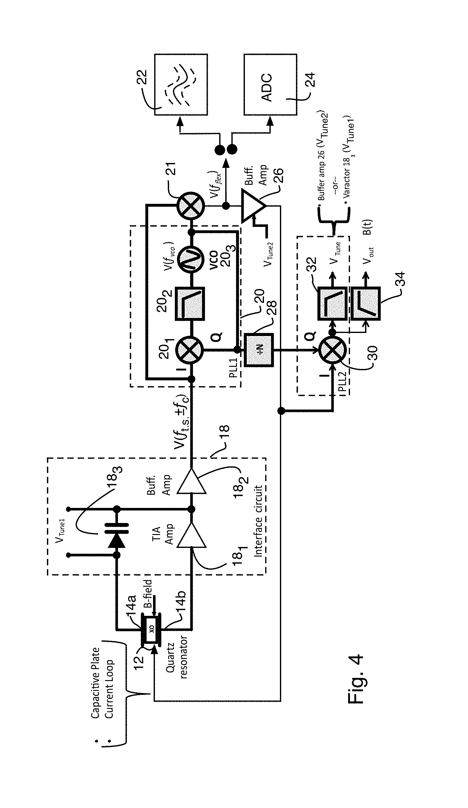
FIG. 4 depicts one embodiment of a circuit for implementing an analog system for implementing closed-loop phase sensitive detection of magnetic field {right arrow over (B)}.
FIG. 4a depicts another embodiment of a circuit for implementing an analog system for implementing closed-loop phase sensitive detection of magnetic field {right arrow over (B)}.
FIG. 5 depicts an embodiment of a circuit for implementing a digital system for implementing closed-loop phase sensitive detection of magnetic field {right arrow over (B)}.
FIG. 6. depicts, on its left hand side a Quartz MEMS magnetometer incorporating capacitive drive electrodes, and also depicts a wafer-level packaged (WLP) Quartz MEMS magnetometer die mounted on a printed-circuit board (PCB) and electrically connected with wire bonds (middle photograph). On the right is the entire Quartz magnetometer PCB showing high frequency output port at the thickness shear carrier frequency (labeled OUT) as well as low-frequency external connections for power supply, current loop control (Cdrv1/2), capacitive plate control (Cap1/2), and thickness shear frequency tuning (Vctrl).
FIG. 7 is a side elevation view similar to FIG. 1b, but FIG. 7 also shows the optional capacitive plates.
DETAILED DESCRIPTION
FIGS. 1a-1d depict the general principles of the Quartz MEMS magnetometer 8 taught by U.S. patent application Ser. No. 14/628,182 filed Feb. 20, 2015 and entitled "A Micro-scale Piezoelectric Resonating Magnetometer" which is referenced above. As is depicted by FIG. 1a, the quartz micro-resonator has a quartz cantilever 10 which is preferably fixed (thus clamped) at one end of same where it is preferably integrally connected to a wider quartz base portion 50 which in turn may be directly anchored or coupled to a substrate 60 which may be made of silicon, for example, and thus comprise a semiconductor substrate with circuitry formed therein. The fabrication of the quartz resonant magnetometer depicted in FIG. 1a preferably mirrors the apparatus and MEMS process that is described in the U.S. patent "Integrated quartz oscillator on an active electronic substrate," U.S. Pat. No. 7,830,074, but with additional metal disposed along the two parallel side edges and along the tip of the quartz cantilever 10 thereby forming an electrically conductive loop 12. When a current is passed around the loop 12 disposed at (or near) the edges of the quartz resonator plate 10 (generated by a drive current source 16 at a frequency f.sub.flex) a Lorentz force {right arrow over (F.sub.B)} is generated in the out-of-plane direction if an external magnetic field {right arrow over (B)} is present with a component along the length of a major axis of the resonator plate 10. This out-of-plane force {right arrow over (F.sub.B)} will drive a flexural vibration mode of the quartz plate 10 (see FIG. 1b where the flexure or flexural mode is identified), resulting in periodic straining of the thickness-shear region of the quartz plate 10 preferably near where the cantilevered quartz plate 10 mates with the wider quartz base portion 50. Note FIG. 7. The thickness shear region of the quartz plate is defined by the location of the electrodes 14a and 14b in FIG. 7. The flexure mode of oscillation is depicted by the two headed arrow in FIG. 1b (and also by the two headed arrow in FIG. 1a adjacent the word "Drive") while the thickness shear mode of vibration is identified by the two parallel arrows adjacent the word "Sense" in FIG. 1a. The periodic straining in aforementioned region, which supports the typical high frequency quartz thickness shear acoustic resonance mode, generates frequency-modulated (FM) sidebands f.sub.flex (see the graph of FIG. 1d) on either side of the thickness shear resonance frequency f.sub.t.s. when the quartz thickness shear mode is driven into oscillation using an interface circuit 18.
There are two distinct oscillation loops in this system. The first is formed by the thickness shear mode of the quartz plate 10 in combination with the interface circuit 18 and this oscillator operates at a high frequency (.about.10 MHz to 10 GHz depending on application requirements). The second is formed by the flexural mode of the quartz plate 10 in combination with feedback provided by a demodulation circuit output at mixer 21 (500 Hz to 1 MHz depending on the flexural mode frequency). When discussing "open loop" and "closed loop" operation herein, reference is being made to the flexural mode oscillation loop, not the thickness shear oscillation loop, which should preferably be understood to be a closed loop oscillation circuit. In "open loop" operation, the current loop 12 or capacitive plates 15 (if used) need to be driven by some external source 16 near the flexural mode frequency of quartz plate 10 to excite the quartz plate 10 into that mode of oscillation. In "closed loop" operation, the current loop 12 is driven by the output of a demodulation circuit at mixer 21 as shown in the embodiments of FIGS. 4, 4a and 5.
The amplitude of the sidebands (see FIG. 1d) at f.sub.flex is proportional to the sensed magnetic field component while f.sub.t.s. is the fundamental oscillatory frequency in thickness shear mode of the cantilevered beam 10.
Since the thickness shear frequency is typically in the tens of MHz to several GHz region, recording the amplitude in a portable device of the sidebands calls for FM demodulating above output signal (the interface circuit 18) to a frequency at which a high resolution analog-to-digital converter (ADC) can accurately digitize the signal. FIG. 2 shows one possible embodiment of a system that can demodulate the magnetometer signal. This system is operates in open loop, because no feedback is provided to the current generator 16 driving the metal loop 12 to hold the loop current at the flexural resonance frequency (f.sub.flex) of the quartz plate 10. How such an open loop system can be constructed from commercial-off-the-shelf (COTS) electronic components will now be described and thereafter closing the loop (that is, convert it to a closed loop system) will be discussed along with phase-sensitive detection, which potentially improves the ultimate resolution of the magnetometer 8 by maintaining a frequency lock onto the flexural resonance of the quartz plate 10.
The system should provide a current to loop 12 having a frequency near the flexural resonance mode of the quartz resonator plate 10 as well as demodulate the thickness-shear oscillation signal to extract the magnetic field signal from the resulting FM sidebands depicted by FIG. 1d. In order to be "near" the flexural resonance mode of the quartz resonator plate 10, the frequency of the current in the loop 12 should preferably fall in the range of f.sub.flex(1-1/Q) to f.sub.flex(1+1/Q), where Q is the quality factor of the flexural resonance mode. Also, modifications to the system are suggested which will enable closed loop operation of the thickness-shear oscillator as well as forming an oscillation loop around the flexural mode of the quartz resonator 8. The closed-loop embodiments of the system (see FIGS. 4 and 5) enable phase-sensitive detection of the magnetic field perturbations, which will greatly enhance the sensitivity and resolution of the quartz magnetometer 8. But before getting to the details of the closed loop embodiments, let us first discuss the open loop embodiment of FIG. 2.
FIG. 2 depicts an embodiment of an open-loop system which is capable of demodulating the FM magnetometer signal provided by the quartz magnetometer 8 (at the output of the sustaining or interface circuit 18) and bring (demodulate) the magnetically-sensitive sidebands back to their native flexural mode frequency (which is low enough in frequency for a high resolution ADC to accurately capture) by the mixer subtracting the thickness-shear carrier frequency (which is synonymous with the thickness shear resonance frequency) such that the sidebands move from f.sub.ts.+-.f.sub.c to simply f.sub.c. A drive current provided by source 16 at a frequency f.sub.c which drives the current loop 12 of the quartz magnetometer 8 in the presence of an external magnetic field {right arrow over (B)}, results in sidebands on the thickness shear carrier frequency offset by multiples of the drive current frequency f.sub.c. In this "open loop" operation of the flexural mode, the source 16 supplies current to the metal loop 12. The frequency of this current is not necessarily at the flexural mode resonance frequency f.sub.flex although it would be desirable if it were so. Anyway, that is why it is referred to as an independent frequency f.sub.c herein.
As is depicted by FIG. 1e, the sidebands appear at offsets of multiples of f.sub.c. They only occur at offsets of f.sub.flex, when the flexural mode is driven in closed loop, that is, when f.sub.c=f.sub.flex (per the discussion above about what "near" means). In the "closed loop" operation of the flexural mode, the function of the current source 16 is replaced by the output of the demodulation circuit at mixer 21. This means that f.sub.c will always be driven toward f.sub.flex by the natural tendency of the flexural oscillation loop to track the flexural mode resonance frequency in a closed loop configuration. And this in turn means that the desired condition above that f.sub.c=f.sub.flex can be achieved for the closed loop embodiments which will give the maximum possible magnetic sensitivity of the sidebands since it will maximize the periodic straining induced by the flexural mode on the thickness shear mode.
The quartz magnetometer 8 is coupled to an interface circuit 18 which preferably has the input of a transimpedance amplifier (TIA) 18.sub.1 coupled to one of the thickness shear sense electrodes 14b of the quartz magnetometer 8. The other thickness shear electrode 14a is coupled in series with an optional varactor 18.sub.3 to an output of TIA 18.sub.1. A tuning voltage is applied across the varactor 18.sub.3 to change its capacitance, resulting in series pulling of the thickness-shear oscillation frequency to a desired target value. The output of TIA 18.sub.1 is coupled to a buffer amplifier 18.sub.2, an output of which forms the output of the interface circuit 18 and hence the magnetically-sensitive output of the quartz magnetometer 8 system.
The output of the interface circuit 18 is fed into a phase-locked loop (PLL) 20, which is preferably formed by a mixer 20.sub.1, a low-pass filter 20.sub.2, and a voltage-controlled oscillator (VCO) 20.sub.3. The mixer 20.sub.1 acts as a phase detector between its I and Q channels. The low pass filter 20.sub.2 blocks high order harmonics of the down-mixed signal at its input. In this way, the output of the filter 20.sub.2 is proportional to the phase difference between the I and Q channels. The phase difference is scaled appropriately using, for example, a tunable gain amplifier (not shown) and fed into the tuning port of the VCO 20.sub.3, which either increases or decreases the frequency of the VCO 20.sub.3 until a lock is achieved between the VCO 20.sub.3 and the incoming signal from the sustaining or interface circuit 18. Hence, the frequency of the VCO 20.sub.3 tracks the thickness-shear frequency of the magnetometer 8, but the output of the VCO 20.sub.3 is free of sidebands. Now the single-tone output of the VCO 20.sub.3 and the magnetometer signal output from the sustaining or interface circuit 18 are mixed together at a down mixer 21, which results in frequency subtraction and brings the sidebands to their native frequency near f.sub.flex. A bandpass filter 22 can optionally be used to remove both DC and higher order modulation products from V(f.sub.c) output by the mixer 21, or the signal V(f.sub.c) can be fed into an analog-digital converter (ADC) 24 and the sideband amplitude can be extracted digitally to obtain a measurement of the strength of the magnetic field sensed by the magnetometer 8.
FIG. 3 depicts a COTS implementation of the FM demodulation system of FIG. 2. First, a differential amplifier (Linear Technologies LT6411) is used to convert the single-ended magnetometer output from sustaining circuit 18 to a differential signal in order to drive the COTS PLL and frequency mixers/dividers. A frequency divider (Analog Devices ADF4007) is used to downconvert the magnetometer signal to a frequency the COTS PLL+VCO (Analog Devices ADF4360-7) can handle (in this implementation, a 600 MHz signal was divided by 8 to 75 MHz for the PLL reference input--note that the division and subsequent multiplication by 8 is an artifact of the specific PLLs used in this implementation. If a different PLL is used (for example, in the case that the thickness shear frequency is changed), this division and multiplication by 8 may not be necessary). Then, the PLL+VCO is used to lock on to the divided magnetometer output signal and generates an output multiplied up by 8 so that it is back at the native thickness shear frequency (again 600 MHz). However, the VCO output is a pure tone without the magnetometer side bands. Finally, the PLL signal and the magnetometer signal are mixed together with a frequency mixer (Analog Devices ADL5801), which is then band-pass filtered and fed to an AC multimeter, or optionally digitized by an ADC.
To maintain maximum sensitivity, it is important for the magnetometer 8 to track the resonance frequency of the flexural mode of the quartz plate 10. This can be achieved by closing the loop between the FM demodulated output from the down-mixed (and optionally filtered) output of the mixer 21 and the current loop 12 drive signal. See the closed loop embodiments of FIGS. 4 and 5. Closed-loop operation will be able to maintain maximum sensitivity over a defined temperature range and will also enables phase-sensitive detection of the magnetometer signal, resulting in improved resolution compared to over open-loop amplitude detection utilized in the embodiments of FIGS. 2 and 3. Hence, a closed-loop quartz magnetometer 8 system will be environmentally robust while maintaining maximum performance. However, in the event that there is no external magnetic field, no Lorentz force can be generated to drive the flexural mode of magnetometer 8 into oscillation. A solution to this problem is to use capacitive driving plates 15a and 15b as shown by FIGS. 6 and 7 and in FIG. 3 of U.S. Pat. No. 8,569,937. Plate 15a is disposed on beam 10 (preferably interiorly of loop 12) while plate 15b is disposed on adjacent fixed structure (fixed relative to the plate 10 which vibrates) such as substrate 60 (see also FIG. 1). By driving the beam 10 into flexural oscillation with capacitive drive plates 15, a force can always be generated, even in the absence of an external magnetic field. Now the external magnetic field {right arrow over (B)} will contribute small perturbations on top of the capacitively-driven flexural mode sidebands seen on the thickness-shear oscillation of FIG. 1. These magnetic field perturbations will induce phase variations proportional to the external magnetic field, which can be read out with the systems shown in FIGS. 4 and 5.
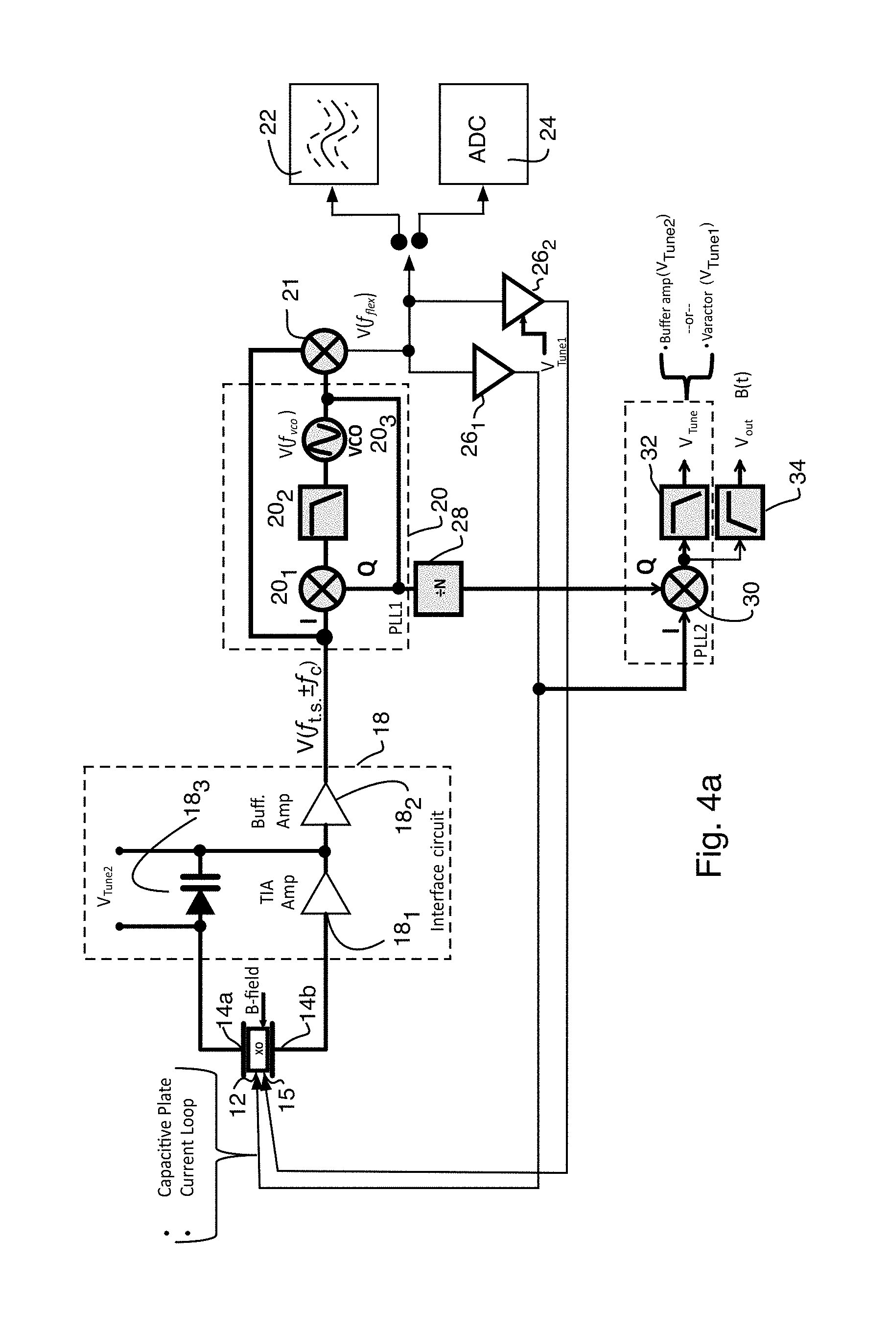
FIG. 4 depicts a embodiment for implementing an analog system for implementing closed-loop phase sensitive detection of magnetic field {right arrow over (B)}. The output of the FM demodulated sidebands from mixer 21 are buffered by a buffer amplifier 26 and fed back to the capacitive drive plates 15. One of the plates 15a or 15b is grounded while the other one of the plates 15a or 15b receives the signal from the buffer amp 26 as well as the current loop 12. The current loop 12 is connected in parallel with the plates 15a & 15b in the embodiment of FIG. 4, but the current loop 12 could alternatively be connected in series with the plates 15a & 15b. The buffer amp 26 may be understood to also provide a DC offset voltage to the AC demodulated signal in order to drive the capacitive plate actuator 15. Hence, in a practical implementation (see FIG. 4a), there are two buffer amplifiers 26.sub.1 and 26.sub.2: one (26.sub.2) for driving the capacitive plate actuator 15 (with DC offset) and another (26.sub.1) to drive the current loop 12 (which does not require a DC offset to function).
FIGS. 4 and 4a show a signal V.sub.tune output from low pass filter 32 being applied to the Buff Amp. 26 (as signal V.sub.tune2) which is preferred over applying V.sub.tune to varactor 18.sub.3 (as signal V.sub.tune1). The preferred implementation is to route the tuning signal V.sub.tune to buffer amp 26 (if optional capacitive plates 15a/b are utilized with the embodiment of FIG. 4) or 26.sub.2 (for the embodiment of FIG. 4a) to adjust the DC level provided by buffer amp 26.sub.2 to the capacitive plates 15a/b which would tune the flexural mode resonance frequency. If V.sub.tune is routed to the varactor 183, then the thickness shear resonance frequency is tuned, but that is less preferred, but may still achieve the goal of making the flexural resonance frequency a specific division ratio (N) of the thickness shear resonance frequency. It may be possible to route "V.sub.tune" to both the varactor 18.sub.3 and buffer amp 26 or 26.sub.2 if stability is not adversely impacted thereby. Otherwise, V.sub.tune1 or V.sub.tune2, whichever one is not connected to V.sub.tune may be connected to a DC voltage when the optional capacitive plates 15 are utilized.
This closes the loop for the flexural mode oscillator and enables sustained oscillation at f.sub.c=f.sub.flex even in the absence of an external magnetic field {right arrow over (B)} (using the capacitive driver plates 15). Note that there are two oscillators in the system, one at the flexural frequency and one at the thickness shear frequency of the magnetometer 8. A small magnetic field change will perturb the phase of the flexural mode oscillator, which can be read out relative to the stable thickness shear frequency when divided appropriately by divider 28. To simplify this division, the thickness shear frequency can be tuned to a multiple of the flexural frequency by providing a second phase-locked loop (PLL2) formed by a mixer 30, a low pass filter 32, and one of the vibration modes of the quartz magnetometer 8. Which vibration mode depends on where V.sub.tune is connected. If V.sub.tune is connected to buffer 26.sub.2, this refers to the flexural mode. If V.sub.tune is connected to varactor 18.sub.3, this would refer to thickness shear mode. The slowly-varying DC component from low pass filter 32 can be used for the phase-lock by controlling either the DC offset of buffer amp 26 (which is the currently preferred embodiment) to tune the flexural resonance frequency of the quartz plate or by controlling the tuning voltage on varactor 18.sub.3 to adjust the thickness shear resonance frequency, while the higher frequency components will be proportional to the magnetic field signal. Hence, low pass (see element 32) and high pass (see element 34) filters (to block the high order demodulation products) can be used to frequency discriminate the desired phase signal proportional to magnetic field strength from the slowly-varying frequency difference between the oscillators required to maintain phase lock.
FIG. 5 depicts a circuit for implementing a digital closed-loop system for implementing closed-loop phase sensitive detection of magnetic field {right arrow over (B)}. The flexural mode and thickness shear mode oscillators are set up in closed loop as described above with reference to FIG. 4. However, in this digital embodiment, the outputs from the buffer amplifier 26 and optionally the divider 28 are directly passed to an ADC 40 and then to a microprocessor 42, where the desired signal processing is done in the digital domain. Feeding the thickness shear resonance to the ADC 32 through a divider 28 can be optionally used as a phase reference, or the divider 28 may be eliminated and a system clock can be used as the phase reference if the system clock is sufficiently stable in frequency. The divider 28 is optional if the system clock is stable enough in frequency to act as a phase reference. If not, then the thickness shear resonance may be used instead (with the divider 28) because it is typically quite stable. As such, the divider 28 depicted in the embodiments of FIGS. 4 and 4a may be omitted and a system clock used instead, if the system clock is sufficiently stable in frequency to act as a phase reference, as the Q input to the mixer 30 in the second phase locked loop PLL2.
The embodiment of FIG. 5 can also be modified to utilize two buffer amplifiers 26.sub.1 and 26.sub.2 with separate connections to loop and capacitive electrodes of the magnetometer 8 as done in the embodiment of FIG. 4a.
FIG. 6 depicts on its left hand side a quartz magnetometer 8 incorporating capacitive drive electrodes 15a and 15b (capacitive drive electrode 15a is on the bottom side of the quartz plate in FIG. 6--see FIG. 7--while capacitive drive electrode 15b is preferably disposed on substrate 60), a current loop 12, and thickness shear electrodes 14 in a single wafer level packaged device. The device may be subsequently die-attached to a substrate 60 (using a pedestal 52 if needed--see FIG. 7--to support the device above the substrate 60) and electrical connections may be made thereto via wirebonds. The external control signals are made with the indicated connectors. Ultimately, the entire electrical system can be implemented on a single application-specific integrated circuit (ASIC), eliminating a majority of the PCB boards in the COTS implementation of FIG. 3.
Obtaining a signal proportional to the strength of magnetic field will now be discussed with reference primarily the "closed loop" implementation depicted in FIG. 4. There are several techniques to obtain a signal output proportional to the magnetic field. One technique takes the output V(f.sub.flex) of down mixer 21 and bandpass filters that signal centered at f.sub.flex by filter 22 and then measures its AC amplitude or digitizes the signal V(f.sub.flex) in an ADC 23 and performs the required filtering and/or signal conditioning in the digital domain. This is the same technique used for the closed loop embodiment of FIG. 2, except that the output of the mixer is V(f.sub.c) instead of V(f.sub.flex).
A second technique, which is appropriate for AC magnetic fields, is to take the system output signal proportional to the magnetic field strength as the output of high pass filter 34. Since the output of mixer 30 is proportional to the phase difference between its I and Q, this technique should allow for very sensitive phase-based detection of the time-varying components of magnetic field.
A third technique based on FIG. 4, but which would require additional hardware, is to insert an IQ generator (generating in-phase and quadrature versions of the output of divider 28) between divider 28 and mixer 30. Then an additional mixer can be placed similarly to mixer 30, but connected to the I channel of theadded IQ generator. In this way, the DC component of the external magnetic field can be measured.
The three techniques discussed above with reference to FIG. 4 could alternatively be used with the embodiment of FIG. 4a. Also, three techniques discussed above with reference to FIG. 4 could alternatively be carried out in the digital domain using the processor of FIG. 5 as opposed to utilizing the discrete electronics discussed with reference to FIG. 4.
It will be noted that the embodiment of FIG. 6 utilizes a trapezoidally shaped active area quartz magnetometer 8 as that taught by U.S. patent application Ser. No. 14/997,160 filed on the same date as this application and entitled "Quartz Magnetometer having a Quartz Resonant Plate with a Broaden Distal End for Enhanced Magnetic Sensitivity" but modified to also include capacitive drive electrodes 15a and 15b disposed preferably interiorly of loop 14. Of course, the cantilevered portion of a magnetometer 8 according to the above just referenced U.S. Patent Application should have a broadened distal end compared to its point of connection to the quartz base portion 50, and thus the embodiment of FIG. 6 can assume other shapes including the tee shaped cantilevered arm shown in the above just referenced US Patent Application.
The foregoing Detailed Description of exemplary and possibly preferred embodiments is presented for purposes of illustration and disclosure in accordance with the requirements of the law. It is not intended to be exhaustive nor to limit the invention to the precise form(s) described, but only to enable others skilled in the art to understand how the invention may be suited for a particular use or implementation. The possibility of modifications and variations will be apparent to practitioners skilled in the art. No limitation is intended by the description of exemplary embodiments which may have included tolerances, feature dimensions, specific operating conditions, engineering specifications, or the like, and which may vary between implementations or with changes to the state of the art, and no limitation should be implied therefrom.
Applicant has made this disclosure with respect to the current state of the art, but also contemplates advancements and that adaptations in the future may take into consideration of those advancements, namely in accordance with the then current state of the art. It is intended that the scope of the invention be defined by the Claims as written and equivalents as applicable.
Reference to a claim element in the singular is not intended to mean "one and only one" unless explicitly so stated. Moreover, no element, component, nor method or process step in this disclosure is intended to be dedicated to the public regardless of whether the element, component, or step is explicitly recited in the Claims.
No claim element herein is to be construed under the provisions of 35 U.S.C. .sctn. 112(f), unless the element is expressly recited using the phrase "means for . . . " and no method or process step herein is to be construed under those provisions unless the step, or steps, are expressly recited using the phrase "comprising the step(s) of . . . ".
* * * * *
D00000
D00001
D00002
D00003
D00004
D00005
D00006
D00007
D00008
D00009
D00010
XML
uspto.report is an independent third-party trademark research tool that is not affiliated, endorsed, or sponsored by the United States Patent and Trademark Office (USPTO) or any other governmental organization. The information provided by uspto.report is based on publicly available data at the time of writing and is intended for informational purposes only.
While we strive to provide accurate and up-to-date information, we do not guarantee the accuracy, completeness, reliability, or suitability of the information displayed on this site. The use of this site is at your own risk. Any reliance you place on such information is therefore strictly at your own risk.
All official trademark data, including owner information, should be verified by visiting the official USPTO website at www.uspto.gov. This site is not intended to replace professional legal advice and should not be used as a substitute for consulting with a legal professional who is knowledgeable about trademark law.