Uniform deposition of SiOC on dielectric and metal surfaces
Jia , et al. April 27, 2
U.S. patent number 10,991,573 [Application Number 16/208,350] was granted by the patent office on 2021-04-27 for uniform deposition of sioc on dielectric and metal surfaces. This patent grant is currently assigned to ASM IP HOLDING B.V.. The grantee listed for this patent is ASM IP Holding BV. Invention is credited to Lingyun Jia, Sun Ja Kim, Viljami Pore, Eva Tois.


| United States Patent | 10,991,573 |
| Jia , et al. | April 27, 2021 |
Uniform deposition of SiOC on dielectric and metal surfaces
Abstract
Plasma enhanced atomic layer deposition (PEALD) processes for simultaneously depositing SiOC on two or more different surfaces of a substrate are provided. For example, SiOC may be deposited simultaneously on a first dielectric surface and a second metal or metallic surface. The PEALD processes can comprise two or more deposition cycles for forming SiOC on the two surfaces. The deposition cycles may comprise alternately and sequentially contacting the substrate with a first precursor comprising silicon and a second plasma reactant, such as an Ar/H.sub.2 plasma. In some embodiments, a PEALD process further comprises contacting the substrate with a plasma reactant prior to beginning the deposition cycle. In some embodiments, the deposition cycle is repeated more than 500 times and a uniform SiOC film may be formed on the two different surfaces.
| Inventors: | Jia; Lingyun (Helsinki, FI), Pore; Viljami (Helsinki, FI), Tois; Eva (Helsinki, FI), Kim; Sun Ja (Helsinki, FI) | ||||||||||
|---|---|---|---|---|---|---|---|---|---|---|---|
| Applicant: |
|
||||||||||
| Assignee: | ASM IP HOLDING B.V. (Almere,
NL) |
||||||||||
| Family ID: | 1000005516754 | ||||||||||
| Appl. No.: | 16/208,350 | ||||||||||
| Filed: | December 3, 2018 |
Prior Publication Data
| Document Identifier | Publication Date | |
|---|---|---|
| US 20190172701 A1 | Jun 6, 2019 | |
Related U.S. Patent Documents
| Application Number | Filing Date | Patent Number | Issue Date | ||
|---|---|---|---|---|---|
| 62594474 | Dec 4, 2017 | ||||
| Current U.S. Class: | 1/1 |
| Current CPC Class: | C23C 16/32 (20130101); H01L 21/0228 (20130101); C23C 16/45536 (20130101); H01L 21/02216 (20130101); H01L 21/02126 (20130101); H01L 21/02274 (20130101); C23C 16/45553 (20130101) |
| Current International Class: | H01L 21/02 (20060101); C23C 16/32 (20060101); C23C 16/455 (20060101) |
References Cited [Referenced By]
U.S. Patent Documents
| 3708728 | January 1973 | Sterling et al. |
| 3925337 | December 1975 | Heiberger |
| 4058430 | November 1977 | Suntola et al. |
| 4282267 | August 1981 | Ku{umlaut over (,)}yel |
| 4389973 | June 1983 | Suntola et al. |
| 4565747 | January 1986 | Nakae et al. |
| 4747367 | May 1988 | Posa |
| 4761269 | August 1988 | Conger et al. |
| 4767494 | August 1988 | Kobayashi |
| 4851095 | July 1989 | Scobey et al. |
| 4935661 | June 1990 | Heinecke et al. |
| 5071670 | December 1991 | Kelly |
| 5166092 | November 1992 | Mochizuki et al. |
| 5221556 | June 1993 | Hawkins et al. |
| 5270247 | December 1993 | Sakuma et al. |
| 5281274 | January 1994 | Yoder |
| 5306666 | April 1994 | Izumi |
| 5316793 | May 1994 | Wallace et al. |
| 5342652 | August 1994 | Foster et al. |
| 5482262 | January 1996 | Hayakawa et al. |
| 5595784 | January 1997 | Kaim et al. |
| 5603771 | February 1997 | Seiberras et al. |
| 5618395 | April 1997 | Gartner |
| 5691235 | November 1997 | Meikle et al. |
| 5693139 | December 1997 | Nishizawa et al. |
| 5711811 | January 1998 | Suntola et al. |
| 5723384 | March 1998 | Park et al. |
| 5744254 | April 1998 | Kampe et al. |
| 5769950 | June 1998 | Takasu et al. |
| 5789024 | August 1998 | Levy et al. |
| 5855680 | January 1999 | Soininen |
| 5916365 | June 1999 | Sherman |
| 5946598 | August 1999 | Yeh |
| 5947710 | September 1999 | Cooper et al. |
| 5964943 | October 1999 | Stein et al. |
| 5965004 | October 1999 | Cowley et al. |
| 5972430 | October 1999 | DiMeo et al. |
| 5973400 | October 1999 | Murakami et al. |
| 6006763 | December 1999 | Mori et al. |
| 6015590 | January 2000 | Suntola et al. |
| 6087257 | July 2000 | Park et al. |
| 6099904 | August 2000 | Mak et al. |
| 6104074 | August 2000 | Chen |
| 6113977 | September 2000 | Soininen et al. |
| 6124158 | September 2000 | Dautartas et al. |
| 6139624 | October 2000 | Rupp |
| 6139700 | October 2000 | Kang et al. |
| 6144060 | November 2000 | Park et al. |
| 6156382 | December 2000 | Rajagopalan et al. |
| 6159871 | December 2000 | Loboda et al. |
| 6162501 | December 2000 | Kim |
| 6174809 | January 2001 | Kang et al. |
| 6188134 | February 2001 | Stumborg et al. |
| 6194310 | February 2001 | Hsu et al. |
| 6200389 | March 2001 | Miller et al. |
| 6203613 | March 2001 | Gates et al. |
| 6206967 | March 2001 | Mak et al. |
| 6234646 | May 2001 | Ito |
| 6270572 | August 2001 | Kim et al. |
| 6284646 | September 2001 | Leem |
| 6287965 | September 2001 | Kang et al. |
| 6342277 | January 2002 | Sherman |
| 6355561 | March 2002 | Sandhu et al. |
| 6380627 | April 2002 | Weihs et al. |
| 6391785 | May 2002 | Satta et al. |
| 6410462 | June 2002 | Yang et al. |
| 6416577 | July 2002 | Suntola et al. |
| 6464779 | October 2002 | Powell et al. |
| 6475276 | November 2002 | Elers et al. |
| 6482262 | November 2002 | Elers et al. |
| 6482733 | November 2002 | Raaijmakers et al. |
| 6482740 | November 2002 | Soininen et al. |
| 6511539 | January 2003 | Raaijmakers |
| 6534395 | March 2003 | Werkhoven et al. |
| 6576053 | June 2003 | Kim et al. |
| 6583048 | June 2003 | Vincent et al. |
| 6599572 | July 2003 | Saanila et al. |
| 6613383 | September 2003 | George et al. |
| 6616982 | September 2003 | Merrill et al. |
| 6632595 | October 2003 | Kikuchi et al. |
| 6652924 | November 2003 | Sherman |
| 6706115 | March 2004 | Leskela et al. |
| 6727169 | April 2004 | Raaijmakers et al. |
| 6780704 | August 2004 | Raaijmakers et al. |
| 6794287 | September 2004 | Saanila et al. |
| 6797340 | September 2004 | Fang et al. |
| 6800383 | October 2004 | Lakhotkin |
| 6800552 | October 2004 | Elers et al. |
| 6809026 | October 2004 | Yoon et al. |
| 6821889 | November 2004 | Elers et al. |
| 6827978 | December 2004 | Yoon et al. |
| 6833161 | December 2004 | Wang et al. |
| 6863727 | March 2005 | Elers et al. |
| 6902763 | June 2005 | Elers et al. |
| 6986914 | January 2006 | Elers et al. |
| 7015153 | March 2006 | Triyoso et al. |
| 7045406 | May 2006 | Huotari et al. |
| 7074690 | July 2006 | Gauri et al. |
| 7115534 | October 2006 | Nguyen et al. |
| 7115974 | October 2006 | Wu et al. |
| 7138336 | November 2006 | Lee et al. |
| 7211144 | May 2007 | Lu et al. |
| 7211508 | May 2007 | Chung et al. |
| 7268078 | September 2007 | Iyer |
| 7329590 | February 2008 | Elers et al. |
| 7405158 | July 2008 | Lai et al. |
| 7410666 | August 2008 | Elers et al. |
| 7416981 | August 2008 | Lee et al. |
| 7611751 | November 2009 | Elers |
| 7749871 | July 2010 | Elers et al. |
| 7776396 | August 2010 | Kobrin et al. |
| 7794798 | September 2010 | Hautala |
| 7824492 | November 2010 | Tois et al. |
| 8217446 | July 2012 | Fukuzumi et al. |
| 8703624 | April 2014 | Yang et al. |
| 9111746 | August 2015 | Ranjan et al. |
| 9171736 | October 2015 | Raley et al. |
| 9243324 | January 2016 | Bowen et al. |
| 9425038 | August 2016 | Shimizu |
| 9425097 | August 2016 | Bouche |
| 9443718 | September 2016 | Harada et al. |
| 9455138 | September 2016 | Fukazawa et al. |
| 9472391 | October 2016 | Shimamoto et al. |
| 9784695 | October 2017 | Blendl |
| 9786491 | October 2017 | Suzuki et al. |
| 9786492 | October 2017 | Suzuki et al. |
| 10424476 | September 2019 | Suzuki et al. |
| 10424477 | September 2019 | Niskanen et al. |
| 10453675 | October 2019 | O'Neill |
| 10600637 | March 2020 | Suzuki et al. |
| 10787591 | September 2020 | Tsotsis et al. |
| 2001/0004479 | June 2001 | Cheung et al. |
| 2001/0005546 | June 2001 | Cheung et al. |
| 2001/0024387 | September 2001 | Raaijmakers et al. |
| 2001/0034097 | October 2001 | Lim et al. |
| 2001/0041250 | November 2001 | Werkhoven et al. |
| 2002/0004293 | January 2002 | Soininen et al. |
| 2002/0104481 | August 2002 | Chiang et al. |
| 2002/0182320 | December 2002 | Leskela et al. |
| 2003/0015764 | January 2003 | Raaijmakers |
| 2003/0026989 | February 2003 | George et al. |
| 2003/0031793 | February 2003 | Chang et al. |
| 2003/0049931 | March 2003 | Byun et al. |
| 2003/0072975 | April 2003 | Shero et al. |
| 2003/0082296 | May 2003 | Elers et al. |
| 2003/0104126 | June 2003 | Fang et al. |
| 2003/0119305 | June 2003 | Huang et al. |
| 2003/0123216 | July 2003 | Yoon et al. |
| 2003/0127043 | July 2003 | Lu et al. |
| 2003/0153181 | August 2003 | Yoon et al. |
| 2003/0157760 | August 2003 | Xi et al. |
| 2003/0161952 | August 2003 | Wang et al. |
| 2003/0181035 | September 2003 | Yoon et al. |
| 2003/0194825 | October 2003 | Law et al. |
| 2003/0203616 | October 2003 | Chung et al. |
| 2004/0130029 | July 2004 | Raaijmakers et al. |
| 2004/0185183 | September 2004 | Srinivasan et al. |
| 2004/0206008 | October 2004 | Sung |
| 2004/0208994 | October 2004 | Harkonen et al. |
| 2004/0224504 | November 2004 | Gadgil |
| 2004/0231799 | November 2004 | Lee et al. |
| 2004/0238876 | December 2004 | Youn et al. |
| 2004/0240820 | December 2004 | Johnson et al. |
| 2005/0037557 | February 2005 | Doczy et al. |
| 2005/0106877 | May 2005 | Elers et al. |
| 2005/0215008 | September 2005 | Orlowski et al. |
| 2005/0236694 | October 2005 | Wu et al. |
| 2005/0271813 | December 2005 | Kher et al. |
| 2006/0019494 | January 2006 | Cao et al. |
| 2006/0078679 | April 2006 | Elers et al. |
| 2006/0079090 | April 2006 | Elers et al. |
| 2006/0079099 | April 2006 | Nguyen et al. |
| 2006/0165892 | July 2006 | Weidman |
| 2006/0211224 | September 2006 | Matsuda et al. |
| 2006/0223300 | October 2006 | Simka et al. |
| 2006/0240187 | October 2006 | Weidman |
| 2007/0054046 | March 2007 | Ishizaka et al. |
| 2007/0072427 | March 2007 | Fukushima |
| 2007/0148350 | June 2007 | Rahtu et al. |
| 2007/0218670 | September 2007 | Ishizaka |
| 2007/0232082 | October 2007 | Balseanu et al. |
| 2007/0251444 | November 2007 | Gros-Jean et al. |
| 2008/0081470 | April 2008 | Clark |
| 2008/0102204 | May 2008 | Elers |
| 2008/0102613 | May 2008 | Elers |
| 2008/0113110 | May 2008 | Elers et al. |
| 2008/0182411 | July 2008 | Elers |
| 2008/0274617 | November 2008 | Milligan |
| 2009/0081868 | March 2009 | Shah et al. |
| 2009/0104791 | April 2009 | Nemani |
| 2009/0211526 | August 2009 | Tanaka et al. |
| 2009/0315093 | December 2009 | Li et al. |
| 2010/0092781 | April 2010 | Zambov et al. |
| 2010/0148903 | June 2010 | Yin et al. |
| 2010/0239742 | September 2010 | Larson-Smith et al. |
| 2010/0297545 | November 2010 | Yoo et al. |
| 2011/0159202 | June 2011 | Matsushita et al. |
| 2011/0262642 | October 2011 | Xiao et al. |
| 2011/0278533 | November 2011 | Hillhouse et al. |
| 2012/0003831 | January 2012 | Kang et al. |
| 2012/0119283 | May 2012 | Lee et al. |
| 2012/0141770 | June 2012 | Cadet et al. |
| 2012/0208347 | August 2012 | Hwang et al. |
| 2012/0269962 | October 2012 | Blomberg et al. |
| 2013/0078454 | March 2013 | Thompson et al. |
| 2013/0084714 | April 2013 | Oka |
| 2013/0112605 | May 2013 | Wyndham et al. |
| 2013/0115763 | May 2013 | Takamure et al. |
| 2013/0134372 | May 2013 | Sakuma et al. |
| 2013/0196082 | August 2013 | Spence |
| 2013/0330935 | December 2013 | Varadarajan |
| 2014/0030432 | January 2014 | Leu et al. |
| 2014/0048131 | February 2014 | Tanaka et al. |
| 2014/0272194 | September 2014 | Xiao et al. |
| 2014/0273477 | September 2014 | Niskanen et al. |
| 2014/0295109 | October 2014 | Sakakura |
| 2014/0302267 | October 2014 | Wynne et al. |
| 2014/0349107 | November 2014 | Thoumazet et al. |
| 2014/0367764 | December 2014 | Lee et al. |
| 2015/0087156 | March 2015 | Kamimura et al. |
| 2015/0118865 | April 2015 | Shimizu |
| 2015/0214103 | July 2015 | Matsuda |
| 2015/0217240 | August 2015 | Van Tuel et al. |
| 2015/0217330 | August 2015 | Haukka et al. |
| 2015/0252477 | September 2015 | Nguyen et al. |
| 2015/0275355 | October 2015 | Mallikarjunan et al. |
| 2015/0303056 | October 2015 | Varadarajan et al. |
| 2015/0303101 | October 2015 | Blomberg et al. |
| 2015/0376211 | December 2015 | Girard et al. |
| 2015/0380302 | December 2015 | Mountsier et al. |
| 2016/0064281 | March 2016 | Izumi et al. |
| 2016/0093485 | March 2016 | Kobayashi et al. |
| 2016/0225616 | August 2016 | Li et al. |
| 2016/0336338 | November 2016 | Song et al. |
| 2017/0140924 | May 2017 | Suzuki et al. |
| 2017/0213726 | July 2017 | Saley et al. |
| 2017/0309476 | October 2017 | Venkatasubramanian et al. |
| 2017/0323782 | November 2017 | Suzuki et al. |
| 2017/0352680 | December 2017 | Shin et al. |
| 2017/0365462 | December 2017 | Varadarajan |
| 2018/0005814 | January 2018 | Kumar et al. |
| 2018/0013078 | January 2018 | Lee et al. |
| 2018/0122742 | May 2018 | Ha et al. |
| 2018/0151355 | May 2018 | Fukazawa |
| 2018/0182618 | June 2018 | Blanquart et al. |
| 2018/0350587 | December 2018 | Jia et al. |
| 104900513 | Sep 2015 | CN | |||
| 0387403 | Sep 1990 | EP | |||
| 0394054 | Oct 1990 | EP | |||
| 0442490 | Aug 1991 | EP | |||
| 0526779 | Feb 1993 | EP | |||
| 0528779 | Feb 1993 | EP | |||
| 0573033 | Dec 1993 | EP | |||
| 0774533 | May 1997 | EP | |||
| 0899779 | Mar 1999 | EP | |||
| 1158070 | Nov 2001 | EP | |||
| 1167567 | Jan 2002 | EP | |||
| 2620440 | Jul 2013 | EP | |||
| 3196336 | Jul 2017 | EP | |||
| 58-033841 | Feb 1983 | JP | |||
| H06-037041 | Feb 1994 | JP | |||
| H06-069157 | Mar 1994 | JP | |||
| H07-230957 | Aug 1995 | JP | |||
| H08-264530 | Oct 1996 | JP | |||
| H0955365 | Feb 1997 | JP | |||
| 09-087857 | Mar 1997 | JP | |||
| 2003342731 | Dec 2003 | JP | |||
| 2004-288979 | Oct 2004 | JP | |||
| 2006-040936 | Feb 2006 | JP | |||
| 2009-083511 | Apr 2009 | JP | |||
| 2010219533 | Sep 2010 | JP | |||
| 2014135475 | Jul 2014 | JP | |||
| 2014229834 | Dec 2014 | JP | |||
| 2015523917 | Aug 2015 | JP | |||
| 2003-0016346 | Feb 2003 | KR | |||
| 2003-0057938 | Jul 2003 | KR | |||
| 2003-0093575 | Dec 2003 | KR | |||
| 2004-0060402 | Jul 2004 | KR | |||
| 2004-0079173 | Sep 2004 | KR | |||
| 2004-0079175 | Sep 2004 | KR | |||
| 2004-0100767 | Dec 2004 | KR | |||
| 2005-0000168 | Jan 2005 | KR | |||
| 2018-005128 | Jan 2018 | KR | |||
| 2010210202 | Jan 2010 | TW | |||
| 201403759 | Jan 2014 | TW | |||
| WO 96/17107 | Jun 1996 | WO | |||
| WO 96/18756 | Jun 1996 | WO | |||
| WO 98/51838 | Nov 1998 | WO | |||
| WO 99/37655 | Jul 1999 | WO | |||
| WO 00/01006 | Jan 2000 | WO | |||
| WO 00/04704 | Jan 2000 | WO | |||
| WO 00/40772 | Jul 2000 | WO | |||
| WO 00/47404 | Aug 2000 | WO | |||
| WO 00/47796 | Aug 2000 | WO | |||
| WO 00/54320 | Sep 2000 | WO | |||
| WO 00/55895 | Sep 2000 | WO | |||
| WO 00/63957 | Oct 2000 | WO | |||
| WO 01/27347 | Apr 2001 | WO | |||
| WO 01/29280 | Apr 2001 | WO | |||
| WO 01/29891 | Apr 2001 | WO | |||
| WO 01/29893 | Apr 2001 | WO | |||
| WO 01/53565 | Jul 2001 | WO | |||
| WO 01/66832 | Sep 2001 | WO | |||
| WO 01/78213 | Oct 2001 | WO | |||
| WO 01/88972 | Nov 2001 | WO | |||
| WO 2004/077515 | Sep 2004 | WO | |||
| WO 2006/080782 | Aug 2006 | WO | |||
| WO 2006/097525 | Sep 2006 | WO | |||
| WO 2007/041089 | Apr 2007 | WO | |||
| WO 2008/051851 | May 2008 | WO | |||
| WO 2008/121478 | Oct 2008 | WO | |||
| WO 2008/137399 | Nov 2008 | WO | |||
| WO 2018/204709 | Nov 2018 | WO | |||
| WO 2018/213018 | Nov 2018 | WO | |||
Other References
|
File History of U.S. Appl. No. 16/811,258, filed Mar. 6, 2020. cited by applicant . 1988RD-0296076 (Nov. 20, 1998), Field effect transistor structure with improved transconductant--contg. spacer-less conducting gate oxide, and tungsten deposited on source and drain, East Version 2.0.1.4 Patent-Assignee: Anonymous[Anon], Sep. 19, 2005. cited by applicant . Aarik et al., "Influence of substrate temperature on atomic layer growth and properties of HfO2 thin films", Thin Solid Films, vol. 340, 1999, pp. 110-116. cited by applicant . Alen et al., "Atomic Layer Deposition of Ta(Al)N(C) Thin Films Using Trimethylaluminum as a Reducing Agent", Journal of the Electrochemical Society, vol. 148, No. 10, pp. G566-G571, 2001. cited by applicant . Andricacos et al., Damascene copper electroplating for chip, IBM Jour. Research and Dev., 1998, vol. 42, Issue 5, pp. 567-574. cited by applicant . Bain et al., Deposition of tungsten by plasma enhanced chemical vapour deposition, J. Phys. IV France, 1999, vol. 9, pp. 827-833. cited by applicant . Chang et al, "Chemical Vapor Deposition of Tantalum Carbide and Carbonitride Thin Films from Me3CE=Ta(CH2CMe3)3 (E = CH, N)," J. Mater. Chem. 13:365-369 (2003). cited by applicant . Chookarjorn et al, "Design of Stable Nanocrystalline Alloys," Science Magazine, vol. 337, pp. 951-954, Aug. 24, 2012. cited by applicant . Closser et al., "Molecular Layer Deposition of a Highly Stable Oxycarbide Thin Film Using an Organic Chlorosilane and Water", ACS Appl. Mater. Interfaces 2018, 10, pp. 24266-24274. cited by applicant . Elers et al., NbC15 as a precursor in atomic layer epitaxy, Applied Surface Science, Jul. 9, 1994, vol. 82/83, pp. 468-474. cited by applicant . Favis et al., Atomic layer epitaxy of silicon, silicon/germanium and silicon carbide via extraction/exchange processes, Avail. NTIS. Report, 1991, pp. 33. cited by applicant . File History of U.S. Appl. No. 14/939,984, filed Nov. 12, 2015. cited by applicant . File History of U.S. Appl. No. 15/707,749, filed Sep. 18, 2017. cited by applicant . File History of U.S. Appl. No. 15/707,878, filed Sep. 18, 2017. cited by applicant . File History of U.S. Appl. No. 15/588,026, filed May 5, 2017. cited by applicant . File History of U.S. Appl. No. 15/787,342, filed Oct. 18, 2017. cited by applicant . File History of U.S. Appl. No. 15/951,626, filed Apr. 12, 2018. cited by applicant . File History of U.S. Appl. No. 15/951,644, filed Apr. 12, 2018. cited by applicant . Fuyuki et al., Atomic layer epitaxy controlled by surface superstructures in silicon carbide, Thin Solid Films, 1993, vol. 225, Issue 1-2, pp. 225-229. cited by applicant . Fuyuki et al., Atomic layer epitaxy of cubic silicon carbide by gas source MBE using surface superstructure, J. Cryst. Growth, 1989, vol. 95, Issue 1-4, pp. 461-463. cited by applicant . Gallis et al., "White light emission from amorphous silicon oxycarbide (a-SiCxOy) thin films: Role of composition and postdeposition annealing", Applied Physics Letters 97, 2010, pp. 0810905-1-0810905-3. cited by applicant . Girolami et al., Tailored Organometallics as Low-Temperature CVD Precursors to Thin Films, Materials Research Society Symposium Proceedings, 1988, vol. 121, pp. 429-438. cited by applicant . Gordon et al., "A Kinetic Model for Step Coverage by Atomic Layer Deposition in Narrow Holes or Trenches", Chemical Vapor Deposition, 2003, vol. 9, No. 2, pp. 73-78. cited by applicant . Hara et al., Atomic layer control of .beta.-silicon carbide (001) surface, Springer Proc. Phys., 1992, pp. 90-95. cited by applicant . Hiltunen et al., Nitrides of titanium, niobium, tantalum and molybdenum grown as thin films by the atomic layer epitaxy method, Thin Solid Films, 1988, vol. 166, pp. 149-154. cited by applicant . Hultman et al., "Review of the Thermal and Mechanical Stability of TiN-based Thin Films" Zeitscrift Fur Metallkunde 90 (10): 803-813 (1999). cited by applicant . Ihanus et al., "ALE growth of ZnS1-xSex thin films by substituting surface sulfur with elemental selenium," Appl. Surface Sci., 112:154-158 (1997). cited by applicant . International Search Report and Written Opinion dated Apr. 7, 2008, Application No. PCT/US2007/082131. cited by applicant . International Search Report and Written Opinion dated Jun. 25, 2015 in Application No. PCT/US2015/023492. cited by applicant . Jehn et al., Gmelin Handbook of Inorganic and Organometallic Chemistry, 8th Edition, 1993, vol. A 5b, Issue 54, pp. 131-154. cited by applicant . Jeon et al., A Study on the Characteristics of TiN Thin Film Deposited by Atomic Layer Chemical Vapor Deposition Method, J. Vac. Sci. Technol. A, 2000, vol. 18, Issue 4, pp. 1595-1598. cited by applicant . Juppo et al., Deposition of copper films by an alternate supply of CuCl and Zn, J. Vac. Sci. Technol A, Jul./Aug. 1997, vol. 15, Issue 4, pp. 2330-2333. cited by applicant . Kattelus et al., "Electrical Properties of Tantalum Based Composite Oxide Films," Mat. Res. Soc. Symp. Proc. vol. 284, pp. 511-516 (1993). cited by applicant . Kattelus et al., "Layered tantalum-aluminum oxide films deposited by atomic layer epitaxy," Thin Solid Films, Vo. 225, pp. 296-298 (1993). cited by applicant . Kim et al., Atomic-layer-deposited WNxCy thin films as diffusion barrier for copper metallization, Applied Physics Letters, Jun. 23, 2003, vol. 82, Issue 25, pp. 4486-4488. cited by applicant . Kim et al., "Novel capacitor technology for high density stand-alone and embedded DRAMs," IEEE International Electron Devices Meeting, IEDM (2000). cited by applicant . Kirk-Othmer, Encyclopedia of Chemical Technology, John Wiley & Sons, Inc., 1992, vol. 4, pp. 841-878. cited by applicant . Klaus et al., Atomic Layer Deposition of Tungsten Nitride Films Using Sequential Surface Reactions, Journal of the Electrochemical Society, 2000, vol. 147, Issue 3, pp. 1175-1181. cited by applicant . Klaus et al., Atomic layer deposition of tungsten using sequential surface chemistry with a sacrificial stripping reaction, Thin Solid Films, 2000, vol. 360, pp. 145-153. cited by applicant . Klaus et al., Atomic layer deposition of tungsten and tungsten nitride using sequential surface reactions, AVS 46th International Symposium, 1999, Seattle, WA, US. cited by applicant . Klaus et al., Atomically controlled growth of tungsten and tungsten nitride using sequential surface reactions, Applied Surface Science, 2000, vol. 162-163, pp. 479-491. cited by applicant . Kukli et al., Properties of (Nb1-xTax)2O5 Solid Solutions and (Nb1-xTax)2O5-ZrO2 Nanolaminates Growth by Atomic Layer Epitaxy, NanoStructured Materials, 1997, vol. 8, pp. 785-793. cited by applicant . Lai et al., Precursors for Organometallic Chemical Vapor Deposition of Tungsten Carbide Films, Chem. Mater., 1995, vol. 7, pp. 2284-2292. cited by applicant . Lakomaa et al., "Surface reactions in AI203 growth from trimethylaluminum and water by atomic layer epitaxy," Applied Surface Science, vol. 107, pp. 107-115 (1996). cited by applicant . Lee et al., "Characteristics of low-k SiOC films deposited via atomic layer deposition", Thin Solid Films 645 (2018), pp. 334-339. cited by applicant . Leskela et al., ALD precursor chemistry: Evolution and future challenges, Jour. Phys. IV France 9, 1999, pp. 837-852. cited by applicant . Ludviksson et al., Low-Temperature Thermal CVD of Ti-Al Metal Films Using a Strong Reducing Agent, Chem. Vap. Deposition, 1998, vol. 4, Issue 4, pp. 129-132. cited by applicant . Martensson, Use of atomic layer epitaxy for fabrication of Si/TiN/Cu structures, J. Vac. Sci. Technol. B, Sep./Oct. 1999, vol. 17, Issue 5, pp. 2122-2128. cited by applicant . Martensson et al., Atomic Layer Epitaxy of Copper and Tantalum, Chemical Vapor Deposition, 1997, vol. 3, Issue 1, pp. 45-50. cited by applicant . Martensson et al., CU(THD)2 As Copper Source in Atomic Layer Epitaxy, Electrochemical Society Proceedings, vol. 97-25, (1997) pp. 1529-1536. cited by applicant . Matsunami et al., Hetero-interface control and atomic layer epitaxy of SiC, Applied Surface Science, 1997, vol. 112, pp. 171-175. cited by applicant . Min et al., Atomic Layer Deposition of TiN Films by Alternate Supply of Tetrakis (ethylmethylamino)- Titanium and Ammonia, Jpn. J. Appl. Phys., 1998, vol. 37, pp. 4999-5004. cited by applicant . Min et al., Atomic Layer Deposition of TiN Thin Films by Sequential Introduction of Ti Precursor and HN3, Mat. Res. Soc. Symp. Proc., 1998, vol. 514, pp. 337-342. cited by applicant . Nakajima et al., Chemical Vapor Deposition of Tungsten Carbide, Molybdenum Carbide Nitride, and Molybdenum Nitride Films, J. Electrochem. Soc., Jun. 1997, vol. 144, Issue 6, pp. 2096-2100. cited by applicant . Polyakov et al., Growth of GaBN Ternary Solutions by Organometallic Vapor Phase Epitaxy, Journal of Electronic Materials, 1997, vol. 26, Issue 3, pp. 237-242. cited by applicant . Ritala et al., Atomic layer epitaxy growth of TiN thin films, J. Electrochem. Soc., 1995, vol. 142, Issue 8, pp. 2731-2737. cited by applicant . Ritala et al., Atomic Layer Epitaxy Growth of TiN Thin Films from Til4 and NH3, J. Electrochem. Soc., Aug. 1998, vol. 145, Issue 8, pp. 2914-2920. cited by applicant . Ritala et al., "Controlled Growth of TaN, Ta3N5, and TaOxNy Thin Films by Atomic Layer Deposition", Chem. Mater., 1999, vol. 11, pp. 1712-1718. cited by applicant . Ritala et al., Effects of intermediate zinc pulses on properties of TiN and NbN films deposited by atomic layer epitaxy, Appl. Surf. Sci., 1997, vol. 120, pp. 199-212. cited by applicant . Ritala et al., Perfectly conformal TiN and Al2O3 films deposited by atomic layer deposition, Chem. Vapor Deposition, 1999, vol. 5, pp. 7-9. cited by applicant . Ritala et al., Surface roughness reduction in atomic layer epitaxy grown of titanium dioxide thin films, Thin Solid Films, vol. 249, pp. 155-162 (1994). cited by applicant . Sadayuki et al., Sub-atomic layer growth of SiC at low temperatures, Japanese Journal of Applied Physics, 1995, vol. 34, Issue 11, pp. 6166-6170. cited by applicant . Sherman et al., Plasma enhanced atomic layer deposition of Ta for diffusion barrier applications, AVS 46th International Symposium, Oct. 26, 1999, Seattle, WA, US. cited by applicant . Song et al., "Formation of Tantalum Carbide and Nitride Phases in Atomic Layer Deposition Using Hydrogen Plasm and tert-Butylimido-tris(diethylamido)-tantalum (TBTDET), and its Effect on Material Properties", Chemical Vapor Deposition, 2008, vol. 14, pp. 334-338. cited by applicant . Suntola, "Atomic Layer Epitaxy," Handbook of Crystal Growth 3, Ch. 14, pp. 601-663 (1994). cited by applicant . Teo et al., "Pre-treatments applied to oxidized aluminum surfaces to modify the interfacial bonding with bis-1, 2-(triethoxysilyl) ethane (BTSE)--Part I. High-purity Al with native oxide", Applied Surface Science 252(5), 2005, pp. 1293-1304. cited by applicant . Teo et al., "Pre-treatments applied to oxidized aluminum surfaces to modify the interfacial bonding with bis-1,2-(triethoxysilyl) ethane (BTSE)--Part II. Anodized 7075-T6 Al alloy", Applied Surface Science 252(5), 2005, pp. 1305-1312. cited by applicant . Tulhoff et al., Ullmann's Encyclopedia of Industrial Chemistry, 5th, Completely Revised Edition, 1986, vol. A5, pp. 61-77. cited by applicant . U.S. Appl. No. 10/049,125, filed Aug. 20, 2002 including prosecution history, including but not limited to, Office Action dated Apr. 8, 2004, Office Action dated Jun. 18, 2003, and Office Action dated Oct. 27, 2003. cited by applicant . U.S. Appl. No. 10/242,368, filed Sep. 12, 2002 including prosecution history, including but not limited to, Office Action dated Oct. 20, 2004, Office Action dated Apr. 27, 2004, and Notice of Allowance dated Jul. 19, 2005. cited by applicant . U.S. Appl. No. 10/969,297, filed Oct. 19, 2004 including prosecution history, including but not limited to, Office Action dated Oct. 11, 2006, Office Action dated Apr. 12, 2007, and Notice of Allowance dated Sep. 18, 2007. cited by applicant . U.S. Appl. No. 11/286,203, filed Nov. 22, 2005 including prosecution history, including but not limited to Office Action dated Sep. 28, 2007. cited by applicant . U.S. Appl. No. 11/288,872, filed Nov. 28, 2005 including prosecution history, including but not limited to, Office Action dated Jul. 2, 2007, Office Action dated Jan. 30, 2008, Office Action dated Sep. 9, 2008, Office Action dated Dec. 4, 2008, and Office Action dated Aug. 20, 2009. cited by applicant . U.S. Appl. No. 11/591,845, filed Nov. 1, 2006 including prosecution history, including but not limited to, Office Action dated Sep. 4, 2008, Office Action dated May 28, 2009, and Notice of Allowance dated Sep. 4, 2009. cited by applicant . U.S. Appl. No. 14/939,984, filed Nov. 12, 2015 including prosecution history, including but not limited to, Office Action dated Feb. 3, 2017, and Notice of Allowance dated Jun. 7, 2017. cited by applicant . U.S. Appl. No. 15/342,943, filed Nov. 3, 2016 including prosecution history, including but not limited to Notice of Allowance dated Jun. 13, 2017. cited by applicant . U.S. Appl. No. 14/255,799, filed Apr. 17, 2014 including prosecution history, including but not limited to, Office Action dated Dec. 1, 2016, Final Office Action dated Aug. 29, 2017, and Advisory Action dated Dec. 21, 2017. cited by applicant . Utriainen et al., "Controlled Electrical Conductivity in SnO2 Thin Films by Oxygen or Hydrocarbon Assisted Atomic Layer Epitaxy," J. Electrochem. Soc. 146(1):189-193 (1999). cited by applicant . Wong et al., Barriers for copper interconnections, Solid State Technology, 1999, pp. 1-7. cited by applicant . Wrobel et al., "Silicon Oxycarbide Films Produced by Remote Microwave Hydrogen Plasma CVD using a Tetramethyldisiloxane Precursor: Growth Kinetics, Structure, Surface Morphology, and Properties", Chem. Vap. Deposition 2015, 21, pp. 307-318. cited by applicant . Yang et al., Atomic Layer Deposition of Tungsten Film from WF6/B2H6: Nucleation Layer for Advanced Semiconductor Devices, Advanced Metallization Conference 2001 (AMC 2001), Conference Proceedings ULSI XVII@2002 Materials Research Society, 2001, pp. 655-660. cited by applicant . Zhang et al., "High permittivity thin film nanolaminates," Journal of Applied Physics, vol. 87, No. 4, pp. 1921-1924 (2000). cited by applicant . Amano et al., "Improved brushing durability of titanium dioxide coating on polymethyl methacrylate substrate by prior treatment with acryloxypropyl trimethoxysilane-based agent for denture application", Dental Materials Journal 2010, 29(1): pp. 97-103. cited by applicant . Diaz-Benito et al., "Hydrolysis study of bis-1,2-(triethoxylsilyl)ethane silane by NMR", Colloids and Surfaces A; Physicochemical and Engineering Aspects, 369 (2010), pp. 53-56. cited by applicant . Ibrahim et al., "Organosilica bis(triethoxysilypethane (BTESE) membranes for gas permeation (GS) and reverse osmosis (RO): The effect of preparation conditions on structure, and the correlation between gas and liquid permeation properties", Journal of Membrane Science, 526 (2017), pp. 242-251. cited by applicant . Wahab et al., "Hybrid periodic mesoporous organosilica materials prepared from 1,2-bis(triethoxysilyl)ethane and (3-cyanopropyl)triethoxysilane", Microporous and Mesoporous Materials 69 (2004), pp. 19-27. cited by applicant . File History of U.S. Appl. No. 16/576,328, filed Sep. 19, 2019. cited by applicant . File History of U.S. Appl. No. 16/603,555, filed Oct. 7, 2019. cited by applicant . File History of U.S. Appl. No. 17/072,480, filed Oct. 16, 2020. cited by applicant. |
Primary Examiner: Fernandes; Errol V
Attorney, Agent or Firm: Knobbe, Martens, Olson & Bear LLP
Parent Case Text
CROSS-REFERENCE TO RELATED APPLICATIONS
The present application claims priority to U.S. provisional application No. 62/594,474, filed Dec. 4, 2017, which is incorporated herein by reference in its entirety.
Claims
What is claimed is:
1. A plasma enhanced atomic layer deposition (PEALD) process for depositing SiOC on two or more different surfaces of a substrate comprising: providing a substrate comprising a first surface and a second surface, wherein the first surface comprises a different material from the second surface, and wherein the first surface is a metal surface and the second surface is a dielectric surface; conducting two or more deposition cycles comprising alternately and sequentially contacting the first and second surfaces of the substrate with a first precursor comprising silicon and a second plasma reactant.
2. The method of claim 1, wherein the dielectric surface comprises SiO.sub.2.
3. The method of claim 1, wherein the metal surface comprises W.
4. The method of claim 1, wherein the plasma reactant comprises Ar/H.sub.2 plasma.
5. The method of claim 1, wherein the plasma reactant does not comprise oxygen species.
6. The method of claim 1, wherein the first precursor is a silicon precursor.
7. The method of claim 1, wherein the silicon precursor has the formula Si(OR.sup.I).sub.4-xR.sup.II.sub.x, wherein x=0 to 3, R.sup.I is alkyl with 1-5 carbons and R.sup.II is any ligand containing carbon and/or hydrogen and/or oxygen and all RI and RII groups can be selected independently.
8. The method of claim 7, wherein R.sup.II has alkenyl, alkynyl, phenyl, carbonyl, aldehyde, ester, ether, carboxyl, peroxy or hydroperoxy functionalities, and wherein all R.sup.I and R.sup.II groups can be chosen independently from each other.
9. The method of claim 7, wherein the first precursor is MPTMS.
10. The method of claim 1, wherein first precursor is MPTMS and the second reactant comprises Ar/H.sub.2 plasma.
11. The method of claim 1, additionally comprising contacting the substrate with a plasma reactant prior to beginning the deposition cycle.
12. The method of claim 1, wherein the SiOC film is deposited uniformly on the first surface and second surface.
13. The method of claim 1, wherein the deposition cycle is repeated more than 500 times.
14. The method of claim 1, wherein the SiOC film has a k value of less than 4.
15. A method of depositing a SiOC thin film on both a first dielectric surface of a substrate and a second metal surface of the same substrate comprising two or more deposition cycles comprising alternately and sequentially contacting the substrate with a first reactant comprising silicon and a second plasma reactant that does not comprise oxygen species.
16. The method of claim 15, wherein the first reactant is MPTMS and the second reactant is plasma generated in Ar/H.sub.2 gas.
17. The method of claim 15, wherein the dielectric surface comprises SiO.sub.2 and the metal surface comprises W.
18. A plasma enhanced atomic layer deposition (PEALD) process for depositing SiOC on a first surface of a substrate comprising SiO.sub.2 and a second surface of the substrate comprising W, the process comprising two or deposition cycles comprising in sequence: contacting the substrate with a first reactant comprising MPTMS; contacting the substrate with a purge gas; contacting the substrate with Ar/H.sub.2 plasma; and contacting the substrate with a purge gas.
19. The method of claim 18, additionally comprising contacting the substrate with a plasma reactant prior to the first deposition cycle.
20. The method of claim 18, wherein the SiOC is deposited uniformly on the first and second surfaces.
Description
BACKGROUND
Field of the Invention
The present application relates generally to plasma enhanced atomic layer deposition (PEALD) of silicon oxide carbide (SiOC).
Description of Related Art
In the semiconductor industry, there is a need to deposit low-K spacers (LKS) on different substrate surfaces with good uniformity. These different surfaces can constitute different materials, for example a metal and a dielectric. Uniform deposition of one material on two or more different substrate surfaces could be beneficial, for example by reducing the number of steps in device fabrication. There is also a need for dielectric materials with low dielectric constant (k) values and low etch rates, for example in acid-based etching solutions such as HF.
SUMMARY
In accordance with one aspect, plasma enhanced atomic layer deposition (PEALD) processes for depositing SiOC on two or more different surfaces of a substrate are provided. In some embodiments the PEALD processes can comprise providing a substrate comprising a first surface and a second surface, where the first surface comprises a different material from the second surface, and conducting two or more deposition cycles for forming SiOC on the two surfaces. The deposition cycles may comprise alternately and sequentially contacting the substrate with a first precursor comprising silicon and a second plasma reactant. In some embodiments, a PEALD process further comprises contacting the substrate with a plasma reactant prior to beginning the deposition cycle. In some embodiments, the deposition cycle is repeated more than 500 times. In some embodiments, the SiOC film is deposited uniformly on the first surface and second surface. In some embodiments, the SiOC film has a k value of less than 4.
In some embodiments, the first surface is a metal surface and the second surface is a dielectric surface. In some embodiments, the dielectric surface comprises SiO.sub.2. In some embodiments, the metal surface comprises W.
In some embodiments, the first precursor is a silicon precursor. In some embodiments, the silicon precursor has the formula Si(OR.sup.I).sub.4-xR.sup.II.sub.x, such that x=0 to 3, R.sup.I is alkyl with 1-5 carbons and R.sup.II is any ligand containing carbon and/or hydrogen and/or oxygen and all RI and RII groups can be selected independently. In some embodiments, R.sup.II has alkenyl, alkynyl, phenyl, carbonyl, aldehyde, ester, ether, carboxyl, peroxy or hydroperoxy functionalities and all R.sup.I and R.sup.II groups can be chosen independently from each other. In some embodiments, the first precursor is MPTMS.
In some embodiments, the plasma reactant comprises Ar/H.sub.2 plasma. In some embodiments, the plasma reactant does not comprise oxygen species.
In some embodiments, the first precursor is MPTMS and the second reactant comprises Ar/H.sub.2 plasma.
In some embodiments, methods of depositing a SiOC thin film on both a first dielectric surface of a substrate and a second metal surface of the same substrate comprise two or more deposition cycles in which the substrate is alternately and sequentially contacted with a first reactant comprising silicon and a second plasma reactant that does not comprise oxygen species. In some embodiments, the first reactant is MPTMS and the second reactant is plasma generated in Ar/H.sub.2 gas. In some embodiments, the dielectric surface comprises SiO.sub.2 and the metal surface comprises W.
In some embodiments, PEALD processes for depositing SiOC on a first surface of a substrate comprising SiO.sub.2 and a second surface of the substrate comprising W are described. The PEALD process may comprise two or more deposition cycles comprising, in sequence: contacting the substrate with a first reactant comprising MPTMS; contacting the substrate with a purge gas; contacting the substrate with Ar/H.sub.2 plasma; and again contacting the substrate with a purge gas. In some embodiments, the process additionally comprises contacting the substrate with a plasma reactant prior to the first deposition cycle. In some embodiments, the SiOC is deposited uniformly on the first and second surfaces.
BRIEF DESCRIPTION OF THE DRAWINGS
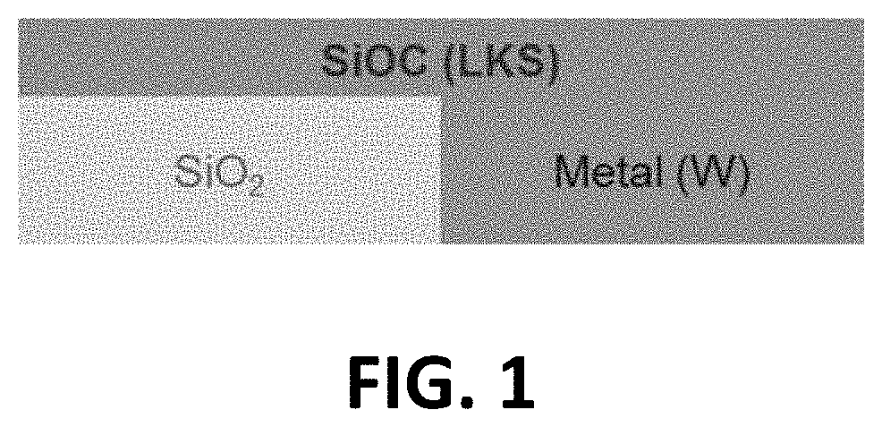
FIG. 1 is a schematic drawing of a uniform SiOC layer deposited on both dielectric and metal surfaces.
FIG. 2 is an STEM of SiOC film deposited on W and SiO.sub.2 pattern at 200.degree. C. and 200 W. The left panel shows the film after 1000 deposition cycles. The right panel shows the film after 500 deposition cycles.
FIG. 3 shows XRR spectra of MPTMS related SiOC deposited on a 12 nm PVD TiN metallic surface after 500 deposition cycles.
DETAILED DESCRIPTION
Silicon oxide carbide (SiOC) films, have a wide variety of applications, as will be apparent to the skilled artisan, for example in integrated circuit fabrication. In some aspects, SiOC films are deposited on two or more different surfaces, for example on a metal surface and a dielectric surface as illustrated in FIG. 1. In some embodiments the SiOC films are deposited on two or more different surfaces by a single deposition process. For example, a SiOC film can be deposited on two different surfaces of a substrate by a plasma-enhanced atomic layer deposition (PEALD) process. In some aspects, SiOC films having low etch rates, for example in HF or dilute HF, are deposited by oxygen-free PEALD processes on a first surface comprising a first material and a second surface comprising a second, different material. In some embodiments the processes use a Si-alkoxy-based precursor and plasma, such as Ar/H.sub.2 plasma. The processes can be controlled to achieve uniform film deposition on a variety of different substrate surfaces.
According to some embodiments a SiOC film is deposited using a PEALD process comprising alternately contacting the substrate with a first silicon alkoxy precursor and a plasma reactant, such as Ar/H.sub.2 plasma. The first precursor may contain both oxygen and silicon. The film grows on a first surface, such as a dielectric surface, and on a second different surface, such as a metal or metallic surface. Excess reactant and/or reaction byproducts may be removed from the substrate surfaces between contacting steps, such as by exposing the substrate to a purge gas.
In some embodiments a substrate is provided comprising a first surface, such as a dielectric surface, and second different surface, such as a metal surface. The substrate is alternately and sequentially contacted with a silicon precursor, such as a silicon alkoxy precursor, and a plasma reactant, such as Ar/H.sub.2 plasma. The plasma and silicon precursor may be provided in pulses separated by a purge in which excess reactant and reaction byproducts, if any, are removed from the substrate surface. In some embodiments the first and second surface are contacted with a purge gas between pulses of the silicon reactant and the plasma.
In some embodiments a deposition process begins with a silicon reactant pulse, and the reaction sequence, or deposition cycle, may be repeated a desired number of times (A): A.times.(silicon precursor pulse/purge/plasma pulse/purge)
In some embodiments the deposition cycle begins with a plasma pulse, which is followed by a silicon precursor pulse.
In some embodiments the deposition cycle is repeated until a uniform SiOC film is deposited on two or more different surfaces. In some embodiments the deposition cycle is repeated at least 100 times, at least 200 times, at least 300 times, at least 400 times, or at least 500 times. In some embodiments the deposition cycle is repeated at least 1000 times. The deposition cycle may be repeated until a film of a desired thickness has been formed on the two or more different surfaces.
By selecting specific process conditions, such as the nature of the reactants, the temperature, the pulse and purge times, the plasma power, and the number of deposition cycles, deposition on two or more different surfaces can be achieved with a desired level of uniformity. In some embodiments, the process conditions, such as plasma power, can be tuned such that growth proceeds uniformly on two or more different surfaces.
In some embodiments a film is considered to be uniformly deposited when it has a thickness that varies by less than 75%, less than 50%, less than 40%, less than 30%, less than 20%, less than 15%, less than 10%, less than 9%, less than 8%, less than 7%, less than 6%, less than 5%, less than 4%, less than 3%, less than 2% or even less than 1% between at least a first surface and a second different surface. In some embodiments thickness is measured as the average thickness of the film deposited on a particular surface. In some embodiments uniformity is measured as the actual thickness variation measured between two different surfaces.
In some embodiments the plasma reactant is hydrogen based. For example, the plasma may be generated in H.sub.2 gas or a mixture of H.sub.2 and a noble gas, such as Ar. In some embodiments the plasma is generated in a mixture of H.sub.2 and Ar gas (referred to as Ar/H.sub.2 plasma). In some embodiments the plasma is oxygen gas-free. That is, the plasma is generated in a gas or gas mixture that does not comprise oxygen.
In some embodiments plasma, for example hydrogen containing plasma, may be generated by applying RF power of from about 5 W to about 5000 W, 10 W to about 2000 W, from about 50 W to about 1000 W, or from about 100 W to about 500 W to a reactant gas or gas mixture. In some embodiments the RF power density may be from about 0.02 W/cm.sup.2 to about 2.0 W/cm.sup.2, or from about 0.05 W/cm.sup.2 to about 1.5 W/cm.sup.2. The RF power may be applied to a gas that flows during the plasma contacting time, that flows continuously through the reaction chamber, and/or that flows through a remote plasma generator. Thus in some embodiments the plasma is generated in situ, while in other embodiments the plasma is generated remotely. In some embodiments a showerhead reactor is utilized and plasma is generated between a susceptor (on top of which the substrate is located) and a showerhead plate.
In some embodiments the deposition rate is similar on both surfaces. In some embodiments the deposition rate differs between the two or more different surfaces. For example, in some embodiments there may be a longer incubation time on one of the surfaces relative to the other. In some embodiments the growth rate on one surface may be different than on the other surface. In some embodiments the deposition rate on one or more surfaces may change over time. For example, the deposition rate on one surface may increase while the deposition rate on a second surface remains constant.
In some embodiments deposition time can be selected to achieve deposition of a SiOC film of similar, relatively uniform thickness on two or more different surfaces, such as on both dielectric and metal surfaces of the same substrate.
In some embodiments the number of deposition cycles is selected to achieve deposition of a SiOC film of a similar, relatively uniform thickness on two or more different surfaces of a substrate.
In some embodiments the deposition process is carried out at a low processing temperature. In some embodiments the deposition temperature is less than about 500.degree. C., less than about 400.degree. C., less than about 300.degree. C., less than about 200.degree. C. or less than about 100.degree. C. In some embodiments a SiOC film is deposited at a temperature of about 100.degree. C. to about 300.degree. C. In some embodiments a SiOC film is deposited at a temperature of about 150.degree. C. to 250.degree. C. In some embodiments a SiOC film is deposited at a temperature of about 200.degree. C.
In some embodiments a SiOC film is deposited on two or more different surfaces comprising different materials in the same deposition process. In some embodiments a SiOC film is deposited uniformly on two or more different surfaces comprising two or more different materials, for example three or more different surfaces each comprising a different material, four or more different surfaces each comprising a different material etc. In some embodiments the two or more different surfaces are on the same substrate. In some embodiments the two or more surfaces are adjacent.
In some embodiments a SiOC film is deposited on all surfaces of a substrate.
In some embodiments, a SiOC film is deposited on two or more different surfaces, where the two or more different surfaces comprise, for example, metal, oxide, oxidized metal, native metal oxide, native SiO.sub.2, Si, dielectric, SiO.sub.2, and/or Si.sub.3N.sub.4.
In some embodiments a SiOC film is deposited on two different surfaces, where one of the surfaces is a dielectric material and the other surface comprises a metal or metallic material.
In some embodiments a dielectric surface may be, for example, a SiO.sub.2 surface or a low-k surface. In some embodiments a dielectric material comprises one or more of SiO.sub.2, SiN and poly Si. In some embodiments a dielectric material is SiO.sub.2. In some embodiments a dielectric material is SiN. In some embodiments a dielectric material is poly-Si.
In some embodiments a SiOC film is deposited on both a first surface and a second, surface that comprises a different material from the first surface. For example, a SiOC film may be deposited on a first metal or metallic surface and a second dielectric surface. In some embodiments a SiOC film is deposited on a SiO.sub.2 surface and a metal surface. In some embodiments a SiOC film is deposited on a SiO.sub.2 surface and a W surface. In some embodiments a SiOC film is deposited on a SiO.sub.2 surface and a TiN surface. In some embodiments a SiOC film is deposited on a W surface and a SiN surface. In some embodiments a SiOC film is deposited on a TiN surface and a SiN surface. In some embodiments a SiOC film is deposited on a W surface and a poly-Si surface. In some embodiment a SiOC film is deposited on a TiN surface and a poly-Si surface.
In some embodiments a SiOC film is deposited with good uniformity on both a first surface and a second surface that comprises a different material from the first surface. For example, a SiOC film may be deposited simultaneously and uniformly on a first metal or metallic surface and a second dielectric surface. In some embodiments a SiOC film is deposited uniformly on a SiO.sub.2 surface and a metal surface. In some embodiments a SiOC film is deposited uniformly on a SiO.sub.2 surface and a W surface. In some embodiments a SiOC film is deposited uniformly on a SiO.sub.2 surface and a TiN surface. In some embodiments a SiOC film is deposited uniformly on a W surface and a SiN surface. In some embodiments a SiOC film is deposited uniformly on a TiN surface and a SiN surface. In some embodiments a SiOC film is deposited uniformly on a W surface and a poly-Si surface. In some embodiment a SiOC film is deposited uniformly on a TiN surface and a poly-Si surface.
Unless otherwise indicated, if a surface is referred to as a metal surface herein, it may be a metal surface or a metallic surface. In some embodiments the metal or metallic surface may comprise metal, metal oxides, and/or mixtures thereof. In some embodiments the metal or metallic surface may comprise surface oxidation. In some embodiments the metal or metallic material of a metal or metallic surface is electrically conductive with or without surface oxidation. In some embodiments a metal or a metallic surface comprises one or more transition metals. In some embodiments the metal or metallic surface comprises one or more of Al, Cu, Co, Ni, W, Nb, and Fe. In some embodiments a metal or metallic surface comprises W. In some embodiments a metal or metallic surface comprises one or more noble metals, such as Ru. In some embodiments a metal or metallic surface comprises a conductive metal oxide, nitride, carbide, boride, or combination thereof. In some embodiments the substrate may comprise a metal nitride, including, but not limited to TiN and/or TaN. In some embodiments the metal surface may comprise a metal carbide. In some embodiments the metal surface may comprise a metal chalcogenide.
The formula of the silicon oxycarbide films is generally referred to herein as SiOC for convenience and simplicity. As used herein, SiOC is not intended to limit, restrict, or define the bonding or chemical state, for example the oxidation state of any of Si, O, C and/or any other element in the film. Further, in some embodiments SiOC thin films may comprise one or more elements in addition to Si, O and C.
In some embodiments the SiOC may comprise from about 0% to about 30% carbon on an atomic basis. In some embodiments the SiOC films may comprise from about 0% to about 60% oxygen on an atomic basis. In some embodiments the SiOC films may comprise about 0% to about 50% silicon on an atomic basis.
In some embodiments the SiOC film has a low-k value. In some embodiments the SiOC film has a k value of less than 4.
In some embodiments the substrate on which deposition is desired, such as a semiconductor workpiece, is loaded into a reaction space or reactor. The reactor may be part of a cluster tool in which a variety of different processes in the formation of an integrated circuit are carried out. In some embodiments a flow-type reactor is utilized. In some embodiments a shower head type of reactor is utilized. In some embodiments, a space divided reactor is utilized. In some embodiments a high-volume manufacturing-capable single wafer ALD reactor is used. In other embodiments a batch reactor comprising multiple substrates is used. For embodiments in which batch ALD reactors are used, the number of substrates is in the range of 10 to 200, in the range of 50 to 150, or in the range of 100 to 130.
Examples of suitable reactors that may be used include commercially available equipment such as the F-120.RTM. reactor, F-450.RTM. reactor, Pulsar.RTM. reactors--such as the Pulsar.RTM. 2000 and the Pulsar.RTM. 3000--EmerALD.RTM. reactor and Advance.RTM. 400 Series reactors, available from ASM America, Inc of Phoenix, Ariz. and ASM Europe B.V., Almere, Netherlands. Other commercially available reactors include those from ASM Japan K.K (Tokyo, Japan) under the tradename Eagle.RTM. XP and XP8.
In some embodiments, if necessary or desired, one or more exposed surfaces of the substrate can be pre-treated to provide reactive sites to react with the first phase of the PEALD process. In some embodiments a separate pre-treatment step is not required. In some embodiments the substrate is pre-treated to provide a desired surface termination. In some embodiments one or more surfaces of the substrate is pre-treated with plasma. In some embodiments the two or more surfaces on which SiOC is to be deposited are pre-treated with plasma, for example with H plasma.
In some embodiments a metal or metallic surface is subject to a surface treatment prior to deposition. For example, a metal or metallic surface may be treated by exposure to a plasma. In some embodiments the metal or metallic surface may be treated with H plasma prior to deposition. In some embodiments a W surface is treated with H plasma prior to deposition.
In some embodiments the substrate is contacted with a first silicon precursor and a second plasma reactant. In some embodiments the deposition process is halogen free. In some embodiments the deposition process is oxygen free.
In some embodiments the silicon precursor has the formula (1.): Si(OR.sup.I).sub.4-xR.sup.II.sub.x
Where x=0 to 3, R.sup.I is alkyl with 1-5 carbons and R.sup.II is any ligand containing carbon and/or hydrogen and/or oxygen. R.sup.II can have, for example, alkenyl, alkynyl, phenyl, carbonyl, aldehyde, ester, ether, carboxyl, peroxy or hydroperoxy functionalities. All R.sup.I and R.sup.II groups can be chosen independently from each other.
In some embodiments the silicon precursor is MPTMS. In the example compound MPTMS, R.sup.I is methyl, R.sup.II is 3-methoxypropyl, and x is 1.
As mentioned above, in some embodiments the PEALD processes do not comprise oxygen plasma or plasma comprising oxygen species.
In some embodiments, for forming SiOC films, each PEALD cycle comprises at least two distinct phases. The contacting and removal of a reactant from the substrate may be considered a phase.
In a first phase, a vapor phase first reactant comprising silicon contacts the substrate and forms no more than about one monolayer on the surface on which deposition is desired. This reactant is also referred to herein as "the silicon precursor," "silicon-containing precursor," or "silicon reactant" and may be, for example, 3-methoxypropyltrimethoxysilane (MPTMS). In some embodiments the first reactant comprises both silicon and oxygen.
In a second phase, a second reactant comprising a reactive species contacts the substrate surfaces and may convert adsorbed silicon to SiOC on the dielectric surface. As discussed above, in some embodiments the second reactant comprises a hydrogen plasma, such as a H.sub.2/Ar plasma.
In some embodiments a gas that is used to form a plasma may flow constantly throughout the deposition process but only be activated intermittently.
In some embodiments a gas that is used to form a plasma does not comprise oxygen. In some embodiments the adsorbed silicon precursor is not contacted with a reactive species generated by a plasma from oxygen. In some embodiments a second reactant comprising reactive species is generated in a gas that does not comprise oxygen. For example in some embodiments a second reactant may comprise a plasma generated in a gas that does not comprise oxygen. In some embodiments the second reactant may be generated in a gas comprising less than about 1 atomic % (at %) oxygen, less than about 0.1 at % oxygen, less than about 0.01 at % oxygen, or less than about 0.001 at % oxygen.
Additional phases may be added and phases may be removed as desired to adjust the composition of the final film.
In some embodiments for depositing a SiOC film, one or more deposition cycles begin by contacting the substrate with the silicon precursor, followed by the second plasma reactant. In other embodiments deposition may begin by contacting the substrate with the second plasma reactant, followed by the silicon precursor.
Excess reactant and reaction byproducts, if any, are removed from the vicinity of the substrate, and in particular from the substrate surface, between reactant contacting phases. In some embodiments excess reactant and reaction byproducts, if any, are removed from the substrate surface by, for example, purging the reaction chamber between reactant contacting phases, such as by purging with an inert gas. The flow rate and contacting time of each reactant is tunable, as is the removal step, allowing for control of the quality and various properties of the films.
The deposition cycle is repeated until a SiOC film of the desired thickness is obtained on the desired surfaces. In some embodiments the deposition parameters, such as the precursor flow rate, contacting time, removal time, and/or reactants themselves, may be varied in one or more deposition cycles during the PEALD process in order to obtain a film with the desired characteristics on two or more different surfaces.
In some embodiments the second plasma reactant is provided in two or more distinct pulses, without introducing another reactant in between any of the two or more pulses. For example, in some embodiments a plasma is provided in two or more sequential pulses, without introducing a Si-precursor in between the sequential plasma pulses. In some embodiments during provision of plasma two or more sequential plasma pulses are generated by providing a plasma discharge for a first period of time, extinguishing the plasma discharge for a second period of time, for example from about 0.1 seconds to about 10 seconds, from about 0.5 seconds to about 5 seconds or about 1.0 seconds to about 4.0 seconds, and exciting it again for a third period of time before introduction of another precursor or a removal step, such as before the Si-precursor or a purge step. Additional pulses of plasma can be introduced in the same way. In some embodiments a plasma is ignited for an equivalent period of time in each of the pulses.
In some embodiments removing excess reactant and reaction byproducts, if any, may comprise purging the reaction chamber. In some embodiments the reaction chamber may be purged by stopping the flow of the second reactant while continuing to flow a carrier gas or purge gas for a sufficient time to diffuse or purge excess reactants and reactant by-products, if any, from the reaction space. In some embodiments the excess second precursor is purged with the aid of inert gas, such as nitrogen or argon, which is flowing throughout the PEALD cycle. In some embodiments the substrate may be moved from the reaction space containing the second reactant to a different reaction space. The removal may, in some embodiments, be from about 0.1 seconds to about 10 seconds, about 0.1 seconds to about 4 seconds or about 0.1 seconds to about 0.5 seconds. Together, the reactive species contacting and removal represent a second, reactive species phase in a SiOC atomic layer deposition cycle.
According to some embodiments of the present disclosure, the pressure of the reaction chamber during processing is maintained at from about 0.01 Torr to about 50 Torr, or from about 0.1 Torr to about 10 Torr. In some embodiments the pressure of the reaction chamber is greater than about 6 Torr, or about 20 Torr.
According to some embodiments a SiOC thin film is deposited on two or more different surfaces of a substrate in a reaction space by a PEALD deposition process comprising at least one cycle comprising:
contacting the substrate with a silicon reactant such that silicon species adsorb onto the surfaces of the substrate;
removing excess silicon reactant and reaction byproducts, if any, from the substrate surface;
contacting the substrate with a second reactant comprising reactive species generated by plasma;
removing excess second reactant and reaction byproducts, if any, from the substrate surface; and
optionally repeating the contacting and removing steps to form a SiOC thin film of a desired thickness and composition on two or more different surfaces.
EXAMPLES
A direct plasma PEALD reactor was used to deposit SiOC films by PEALD using 3-Methoxypropyl(trimethoxysilane) (MPTMS) as the silicon precursor. No heating of the precursor to produce vapor-phase reactant was required due to high enough vapor pressure of the compound. Experiments were carried out at a deposition temperature of 200.degree. C. The growth rate per cycle (GPC) of the process was typically -0.2 .ANG./c. FIG. 2 shows SEM images of SiOC films deposited at 200.degree. C. on a substrate comprising adjacent horizontal surfaces of W and SiO2.
As shown in the FIG. 2, right frame, after 500 cycles, SiOC film deposited was deposited on the SiO.sub.2 surface while almost no deposition was observed on the adjacent W surface. However, after a longer deposition time as shown in FIG. 2, left frame, specifically 1000 cycles, SiOC was deposited to a similar extent on both the W and the SiO.sub.2 surface. While some difference in the thickness of the SiOC layer can be observed between the W and SiO.sub.2 surfaces, the thickness difference is expected to diminish with even longer deposition. The results observed indicate that there was a longer incubation time for SiOC deposition on the W surface than on SiO.sub.2 surface.
FIG. 3 shows that around 6.2 nm of SiOC film was deposited on a TiN surface using MPTMS as the silicon precursor after 500 cycles, which indicates a slightly lower growth per cycle than that observed on native oxide surfaces.
* * * * *
D00000
D00001
D00002
D00003
XML
uspto.report is an independent third-party trademark research tool that is not affiliated, endorsed, or sponsored by the United States Patent and Trademark Office (USPTO) or any other governmental organization. The information provided by uspto.report is based on publicly available data at the time of writing and is intended for informational purposes only.
While we strive to provide accurate and up-to-date information, we do not guarantee the accuracy, completeness, reliability, or suitability of the information displayed on this site. The use of this site is at your own risk. Any reliance you place on such information is therefore strictly at your own risk.
All official trademark data, including owner information, should be verified by visiting the official USPTO website at www.uspto.gov. This site is not intended to replace professional legal advice and should not be used as a substitute for consulting with a legal professional who is knowledgeable about trademark law.