Plug module system
Dambach , et al. March 16, 2
U.S. patent number 10,950,997 [Application Number 15/546,563] was granted by the patent office on 2021-03-16 for plug module system. This patent grant is currently assigned to Molex, LLC. The grantee listed for this patent is Molex, LLC. Invention is credited to Philip J. Dambach, Kent E. Regnier.
View All Diagrams
| United States Patent | 10,950,997 |
| Dambach , et al. | March 16, 2021 |
Plug module system
Abstract
A plug module is provided that includes a first mating end and a second mating end. The first mating end is configured to mate with a predefined port, such as a QSFP port. The second mating end can support two or more micro receptacles that allow the plug module to provide an octopus-like cable assembly without requiring the predetermination of a particular length of cable.
| Inventors: | Dambach; Philip J. (Naperville, IL), Regnier; Kent E. (Lombard, IL) | ||||||||||
|---|---|---|---|---|---|---|---|---|---|---|---|
| Applicant: |
|
||||||||||
| Assignee: | Molex, LLC (Lisle, IL) |
||||||||||
| Family ID: | 1000005426599 | ||||||||||
| Appl. No.: | 15/546,563 | ||||||||||
| Filed: | January 27, 2016 | ||||||||||
| PCT Filed: | January 27, 2016 | ||||||||||
| PCT No.: | PCT/US2016/015098 | ||||||||||
| 371(c)(1),(2),(4) Date: | July 26, 2017 | ||||||||||
| PCT Pub. No.: | WO2016/123204 | ||||||||||
| PCT Pub. Date: | August 04, 2016 |
Prior Publication Data
| Document Identifier | Publication Date | |
|---|---|---|
| US 20180026413 A1 | Jan 25, 2018 | |
Related U.S. Patent Documents
| Application Number | Filing Date | Patent Number | Issue Date | ||
|---|---|---|---|---|---|
| 62108276 | Jul 27, 2015 | ||||
| Current U.S. Class: | 1/1 |
| Current CPC Class: | H01R 13/6275 (20130101); H01R 13/6461 (20130101); H01R 31/005 (20130101); H01R 24/60 (20130101); H01R 24/62 (20130101); H01R 2107/00 (20130101) |
| Current International Class: | H01R 31/00 (20060101); H01R 24/60 (20110101); H01R 24/62 (20110101); H01R 13/6461 (20110101); H01R 13/627 (20060101) |
| Field of Search: | ;439/638 |
References Cited [Referenced By]
U.S. Patent Documents
| 5549488 | August 1996 | Berndt et al. |
| 5966487 | October 1999 | Gilliland |
| 6738474 | May 2004 | Miller |
| 7195404 | March 2007 | Dudley |
| 7238049 | July 2007 | Wu |
| 7258264 | August 2007 | Ice |
| 7309250 | December 2007 | Reed |
| 7416436 | August 2008 | Togami |
| 7438565 | October 2008 | Hamazaki |
| 7452139 | November 2008 | Wang |
| 7540755 | June 2009 | Wu |
| 7594766 | September 2009 | Sasser |
| 7625240 | December 2009 | Hayden, Sr. |
| 7941053 | May 2011 | Dallesasse |
| 7959467 | June 2011 | Sasser |
| 8083417 | December 2011 | Aronson |
| 8083547 | December 2011 | Roth |
| 8121139 | February 2012 | Sunaga |
| 8186891 | May 2012 | Hudgins |
| 8267712 | September 2012 | Huang |
| 8267718 | September 2012 | Straka |
| 8417119 | April 2013 | Shimoosako |
| 8469608 | June 2013 | Kurashima |
| 8526810 | September 2013 | Cole |
| 8573857 | November 2013 | Hoffmann |
| 8740473 | June 2014 | Katoh |
| 8807846 | August 2014 | Hung |
| 8858095 | October 2014 | Meng |
| 9001515 | April 2015 | Tang |
| 9083130 | July 2015 | Casher |
| 9235013 | January 2016 | Chan |
| 9312618 | April 2016 | Regnier |
| 9320160 | April 2016 | Dudemaine |
| 9341795 | May 2016 | Luo |
| 9419403 | August 2016 | Faith |
| 9478884 | October 2016 | Tsai |
| 9538637 | January 2017 | Zhao |
| 9590737 | March 2017 | Tang |
| 9620894 | April 2017 | Potterf |
| 9703053 | July 2017 | Kagaya |
| 9711901 | July 2017 | Scholeno |
| 9711908 | July 2017 | Yao |
| 9810873 | November 2017 | McColloch |
| 9819125 | November 2017 | Regnier |
| 9831610 | November 2017 | Sutter |
| 9882314 | January 2018 | Casher |
| 10193268 | January 2019 | Chow |
| 10320482 | June 2019 | Chou |
| 2003/0020986 | January 2003 | Pang |
| 2005/0152701 | July 2005 | Liu |
| 2007/0049100 | March 2007 | Tsai |
| 2007/0059953 | March 2007 | Togami |
| 2007/0072457 | March 2007 | Hamazaki |
| 2007/0110374 | May 2007 | Oki |
| 2007/0237464 | October 2007 | Aronson |
| 2008/0112674 | May 2008 | Andersson |
| 2008/0145003 | June 2008 | Ice |
| 2009/0180784 | July 2009 | Kagaya |
| 2010/0029104 | February 2010 | Patel |
| 2010/0061069 | March 2010 | Cole |
| 2010/0087084 | April 2010 | George |
| 2012/0220152 | August 2012 | Wu |
| 2012/0251057 | October 2012 | Yi et al. |
| 2012/0281365 | November 2012 | Lima |
| 2013/0005178 | January 2013 | Straka et al. |
| 2013/0156418 | June 2013 | Stapleton |
| 2014/0348468 | November 2014 | Lagziel |
| 2014/0349496 | November 2014 | Zhu |
| 2014/0363171 | December 2014 | Tang |
| 2015/0333460 | November 2015 | Regnier et al. |
| 2016/0131854 | May 2016 | de Jong |
| 2016/0238805 | August 2016 | McColloch |
| 2017/0077643 | March 2017 | Zbinden |
| 87100361 | Aug 1987 | CN | |||
| 102650978 | Aug 2012 | CN | |||
| 102870027 | Jan 2013 | CN | |||
| 104020535 | Sep 2014 | CN | |||
| WO 2014113563 | Jul 2014 | WO | |||
Parent Case Text
RELATED APPLICATIONS
This application claims priority to International Application No. PCT/US2016/015098, filed Jan. 27, 2016, which claims priority to U.S. Provisional Application No. 62/108,276, filed Jan. 27, 2015, which is incorporated herein by reference in its entirety.
Claims
What is claimed is:
1. A plug module, comprising: a body with a first mating end and a second mating end, the first end configured to be inserted into a predefined port; a paddle card positioned in the first end and including a plurality of contact pads, the paddle card configured to receive at least two transmit channels and two receive channels; a first micro receptacle and a second micro receptacle supported in the second mating end, wherein the first and second micro receptacle are each configured to include one of the two transmit channels and one of the two receive channels; and a micro board that supports the first and second micro receptacles, the first micro receptacle being mounted on the micro board and the second micro receptacle being mounted on the micro board.
2. The module of claim 1, wherein at least one cable connects the micro board to the paddle card.
3. The module of claim 1, wherein the micro receptacles are positioned on two sides of the micro board and the micro board is offset upward compared to the paddle card.
4. The module of claim 1, wherein each micro receptacle has at least 8 pins arranged on a 0.5 mm pitch.
5. The module of claim 1, wherein each micro receptacle includes an individual latch, each latch configured, in operation, to releasably engage a mating micro plug module.
6. A plug module system, comprising: a plug module as defined in claim 5; and a cable assembly mated to the plug module, the cable assembly including a micro plug connector with terminals at a 0.5 mm pitch, wherein the micro receptacle and the micro plug connector are configured to support 12.5 GHz signaling over a transmit channel and a receive channel with less than 35 dB far end crosstalk.
7. The module system of claim 6, wherein the cable assembly has an SFP connector mounted on the other end.
8. The module system of claim 6, wherein a plurality of cable assemblies are mounted to the plug module, wherein one of the plurality of cable assemblies has a first length and another of the plurality of cables assembles has a second length, the first length being different than the second length.
9. The module of claim 1, wherein at least one cable electrically connects the paddle card to at least one of the first micro receptacle and the second micro receptacle.
10. The module of claim 9, wherein the at least one cable connects the paddle card to the at least one of the first micro receptacle and the second micro receptacle.
11. The module of claim 1, wherein flex circuitry electrically connects the paddle card to at least one of the first micro receptacle and the second micro receptacle.
12. The module of claim 1, wherein the micro board comprises a planar circuit board.
13. The module of claim 1, wherein the module further comprises circuitry that includes at least one of a retimer and an amplifier.
14. A plug module, comprising: a body with a first mating end and a second mating end, the first end configured to be inserted into a predefined port; a paddle card positioned in the first mating end and including a plurality of contact pads, the paddle card configured to receive at least two transmit channels and two receive channels; a first micro receptacle and a second micro receptacle supported in the second mating end, wherein the first and second micro receptacle are each configured to include one of the two transmit channels and one of the two receive channels; and a micro board that supports the first and second micro receptacles, the first micro receptacle being mounted on a first side of the micro board and the second micro receptacle being mounted on a second side of the micro board, the first side of the micro board being opposite the second side of the micro board.
15. The plug module of claim 14, wherein at least one cable electrically connects the paddle card to at least one of the first micro receptacle and the second micro receptacle.
16. The plug module of claim 15, wherein the at least one cable connects the paddle card to the at least one of the first micro receptacle and the second micro receptacle.
17. The plug module of claim 14, wherein flex circuitry electrically connects the paddle card to at least one of the first micro receptacle and the second micro receptacle.
18. The plug module of claim 14, wherein the micro board comprises a planar circuit board.
19. The plug module of claim 14, wherein the plug module fluffier comprises circuitry that includes at least one of a retimer and an amplifier.
20. The plug module of claim 14, wherein each micro receptacle has at least 8 pins arranged on a 0.5 mm pitch.
Description
TECHNICAL FIELD
This disclosure relates to the field of input/output (IO) connectors, more specifically to IO connectors suitable for use in high data rate applications.
DESCRIPTION OF RELATED ART
Input/output (IO) connectors that have four communication channels (e.g., 4 transmits and 4 receives) are known. One example is the quad small form-factor pluggable (QSFP) connector. These types of connectors are suited to support high bandwidth applications due to the inclusion of the four communication channels.
One issue that sometimes comes up with a connector such as the QSFP style connector is that there is a desire to have a large amount of bandwidth available on a switch that is positioned as a Top of Rack (ToR) switch but the bandwidth available in one QSFP port provided in such a ToR switch might be greater than another single port really needs. The desire to break out the channel sometimes existed in standard QSFP products that provided 40 Gbps and this desired is expected to become a more prevalent issue in products designed to support 100 Gbps, such as 100 Gbps capable QSFP products.
One existing way to address this issue is to have what is sometime referred to as a break-out cable or octopus cable. For example, a cable assembly could have a QSFP plug module on one end and have four cables extending from the QSFP plug to four separate small form-factor pluggable (SFP) style plug modules. This allows a single QSFP port to communicate with 4 SFP ports and, for high performing assemblies, each communication channel can support 25 Gbps of bidirectional communication. While this is an effective way to break out the four communication channels so as to allow one port to communicate with four other ports, the use of octopus cables is generally disfavored. One issue is that a cable from a ToR switch will have to reach lengths of less than a foot to more than a meter. As can be appreciated, it is difficult to know in advance how far each cable of an octopus cable assembly is going to need to reach. Therefore it is common to select a length that is long enough for all cases but is too long for most cases. This tends to result in a mess of cables that is difficult to understand or work with once installed. Consequentially, certain individuals would appreciate further improvements in connector configurations.
SUMMARY
A plug module is disclosed that includes a first mating end that is configured to mate with a predefined port (such as a conventional connector receptacle) and has a second mating end that includes a plurality of micro receptacles. A paddle card can be positioned at the first mating end and the micro receptacles can be supported so that they are offset upward, compared to the paddle card. A plurality of cable assemblies with micro plugs can be connected to the plurality of micro receptacles such that each cable assembly can offer a different length and have a desired far end termination configuration.
BRIEF DESCRIPTION OF THE DRAWINGS
The present invention is illustrated by way of example and not limited in the accompanying figures in which like reference numerals indicate similar elements and in which:
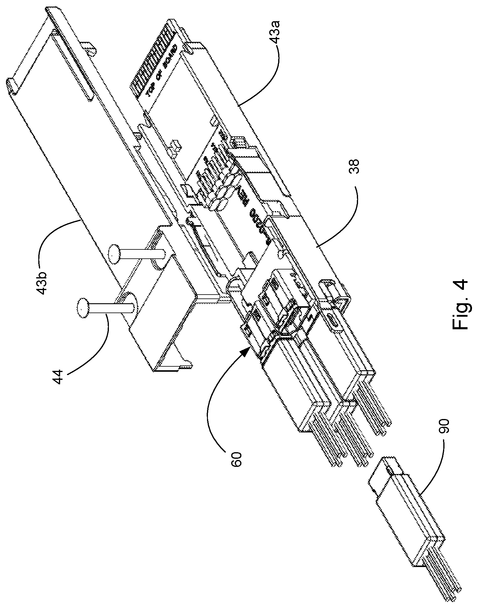
FIG. 1 illustrates a perspective view of an embodiment of a break out connector module.
FIG. 2 illustrates a simplified perspective view of the embodiment depicted in FIG. 1.
FIG. 3 illustrates a perspective, partially exploded view of the embodiment depicted in FIG. 2.
FIG. 4 illustrates an exploded perspective view of the embodiment depicted in FIG. 2.
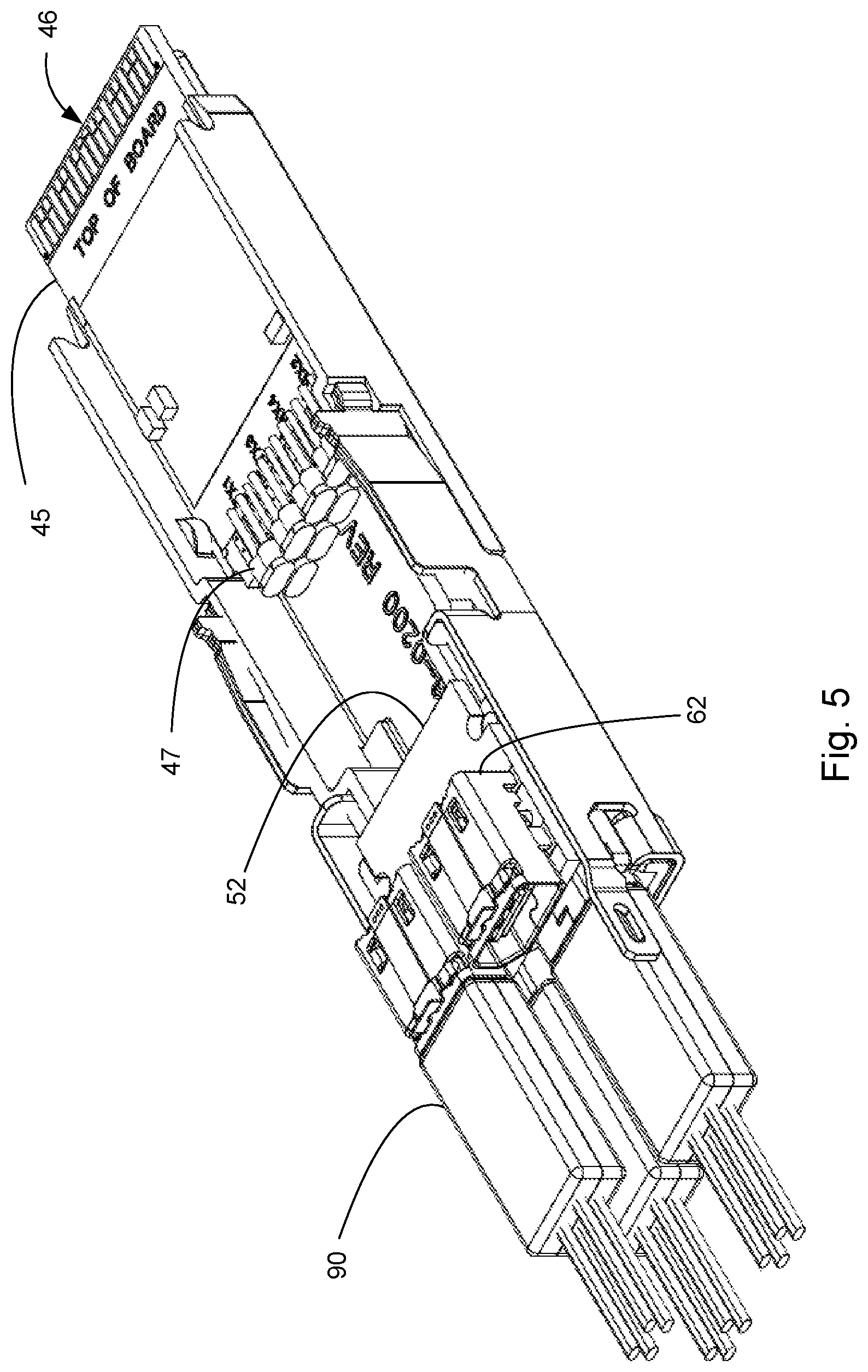
FIG. 5 illustrates a perspective simplified view of the embodiment depicted in FIG. 4.
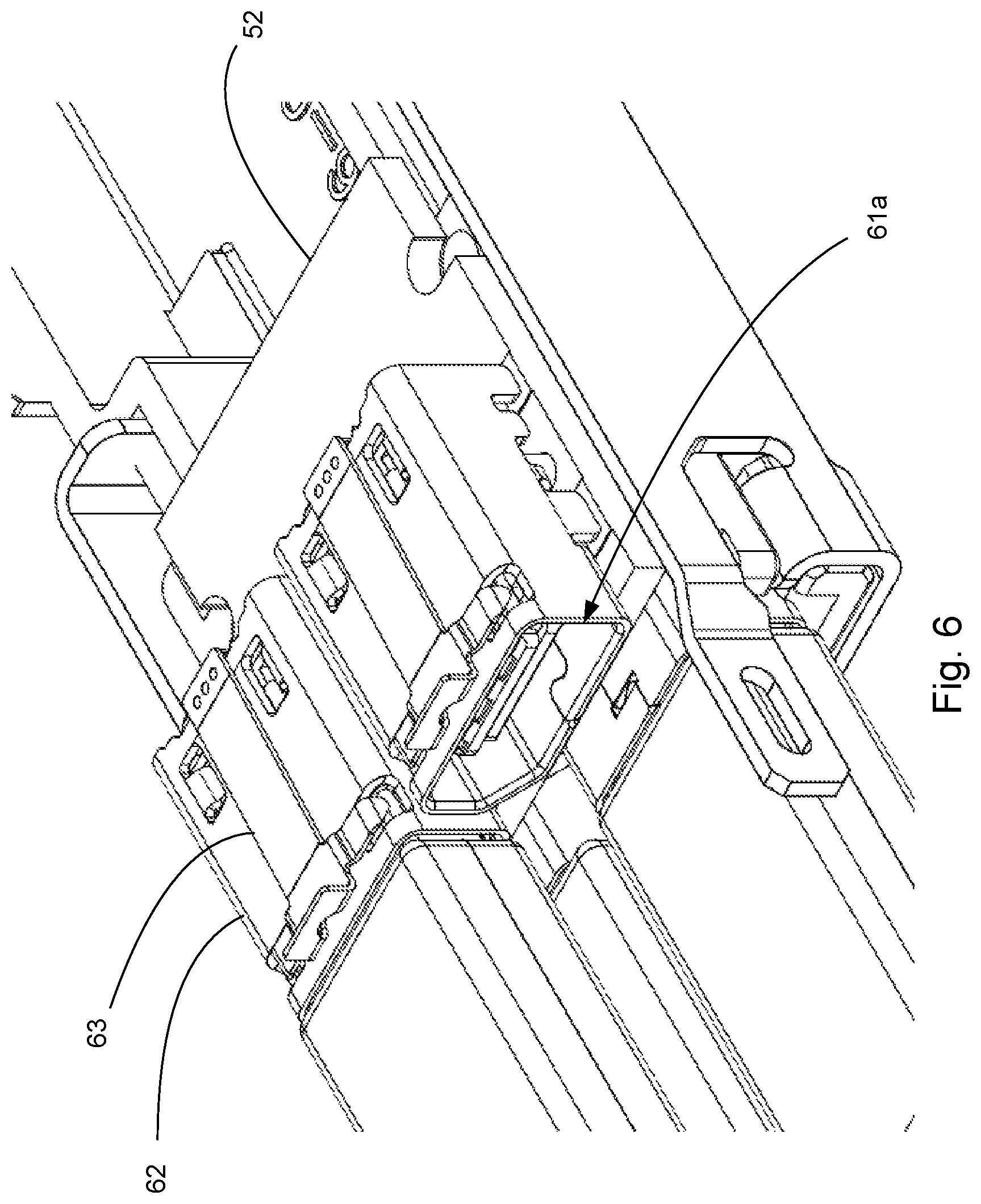
FIG. 6 illustrates a perspective enlarged view of the embodiment depicted in FIG. 5.
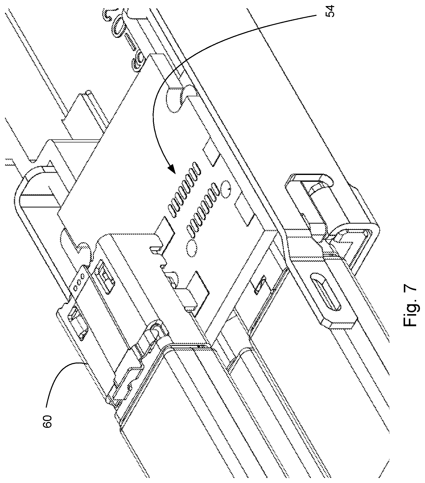
FIG. 7 illustrates a perspective simplified view of the embodiment depicted in FIG. 6.
FIG. 8 illustrates a perspective view of the embodiment depicted in FIG. 7.
FIG. 9 illustrates a perspective view of the embodiment depicted in FIG. 8 but with a latch in a second position.
FIG. 10 illustrates a perspective view of an embodiment of a break out module with the latch system removed.
FIG. 11 illustrates a perspective view of an embodiment of a circuit board supporting four connectors.
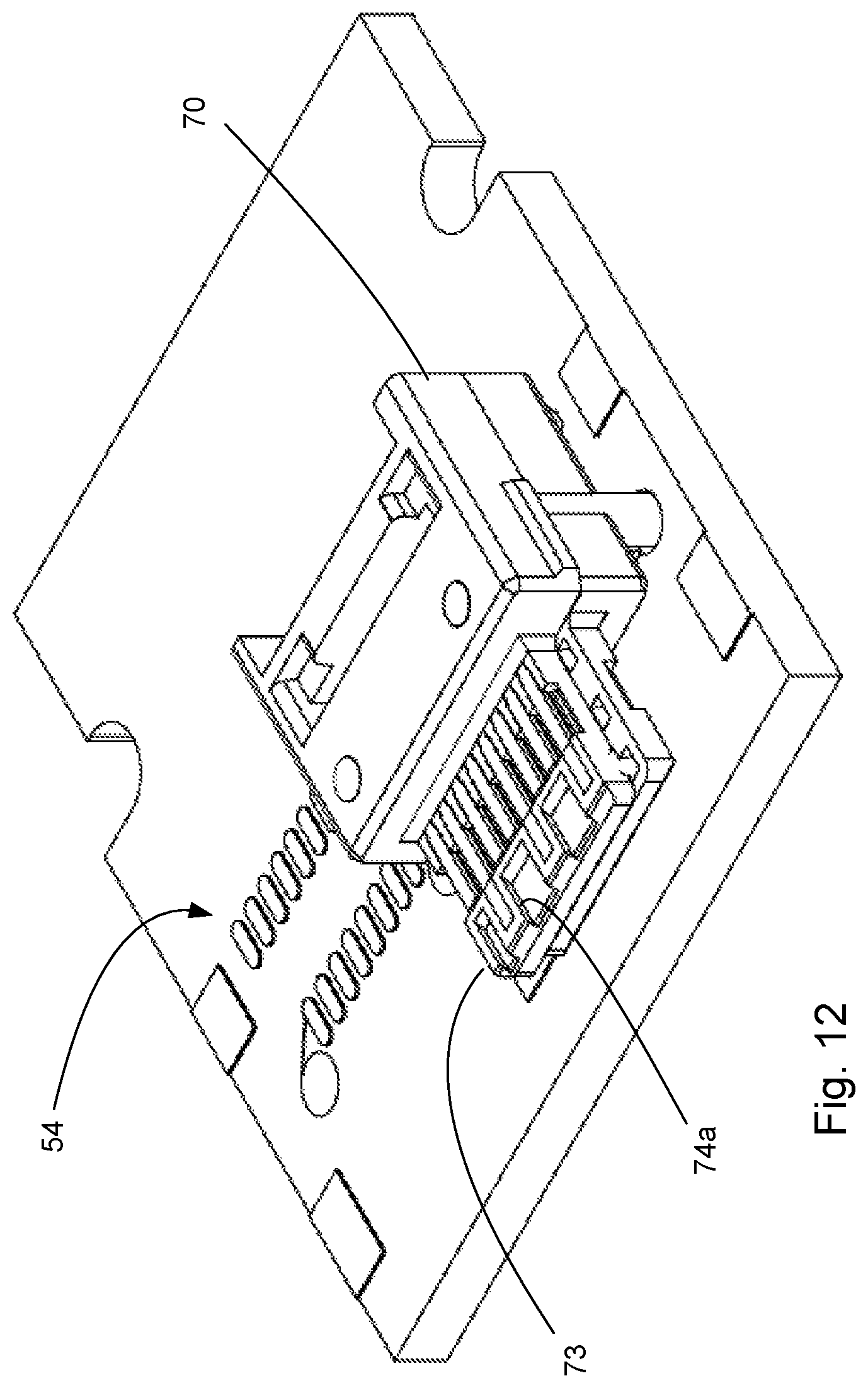
FIG. 12 illustrates a perspective simplified view of the embodiment depicted in FIG. 11 with just one connector housing positioned on the circuit board.
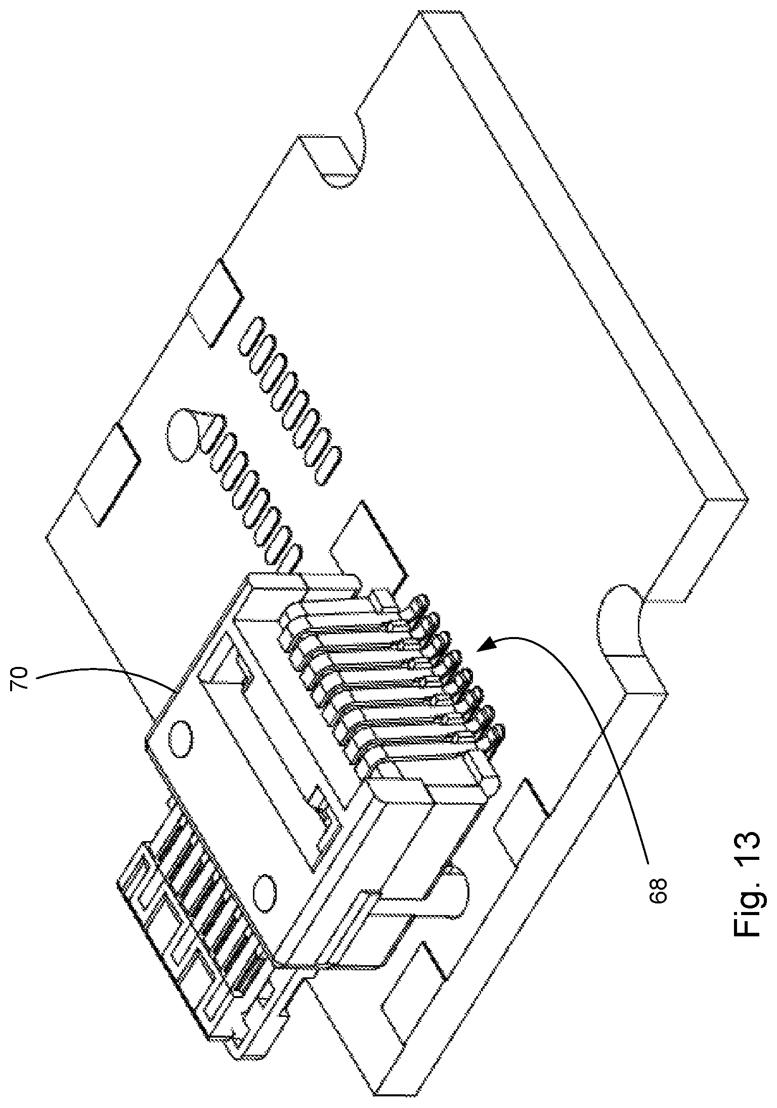
FIG. 13 illustrates another perspective view of the embodiment depicted in FIG. 12.
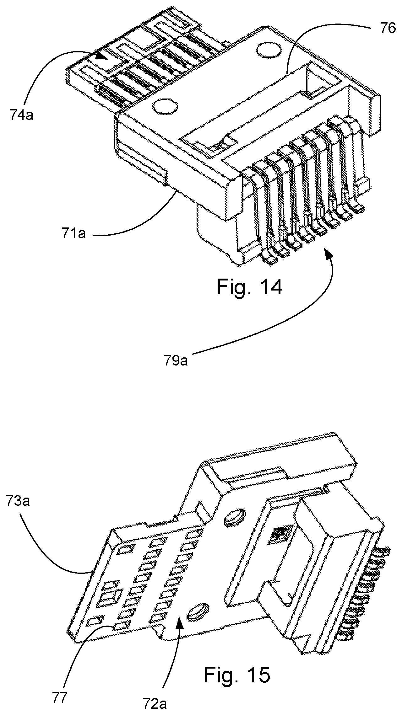
FIG. 14 illustrates a perspective view of an embodiment of a first housing wafer.
FIG. 15 illustrates another perspective view of the embodiment depicted in FIG. 14.
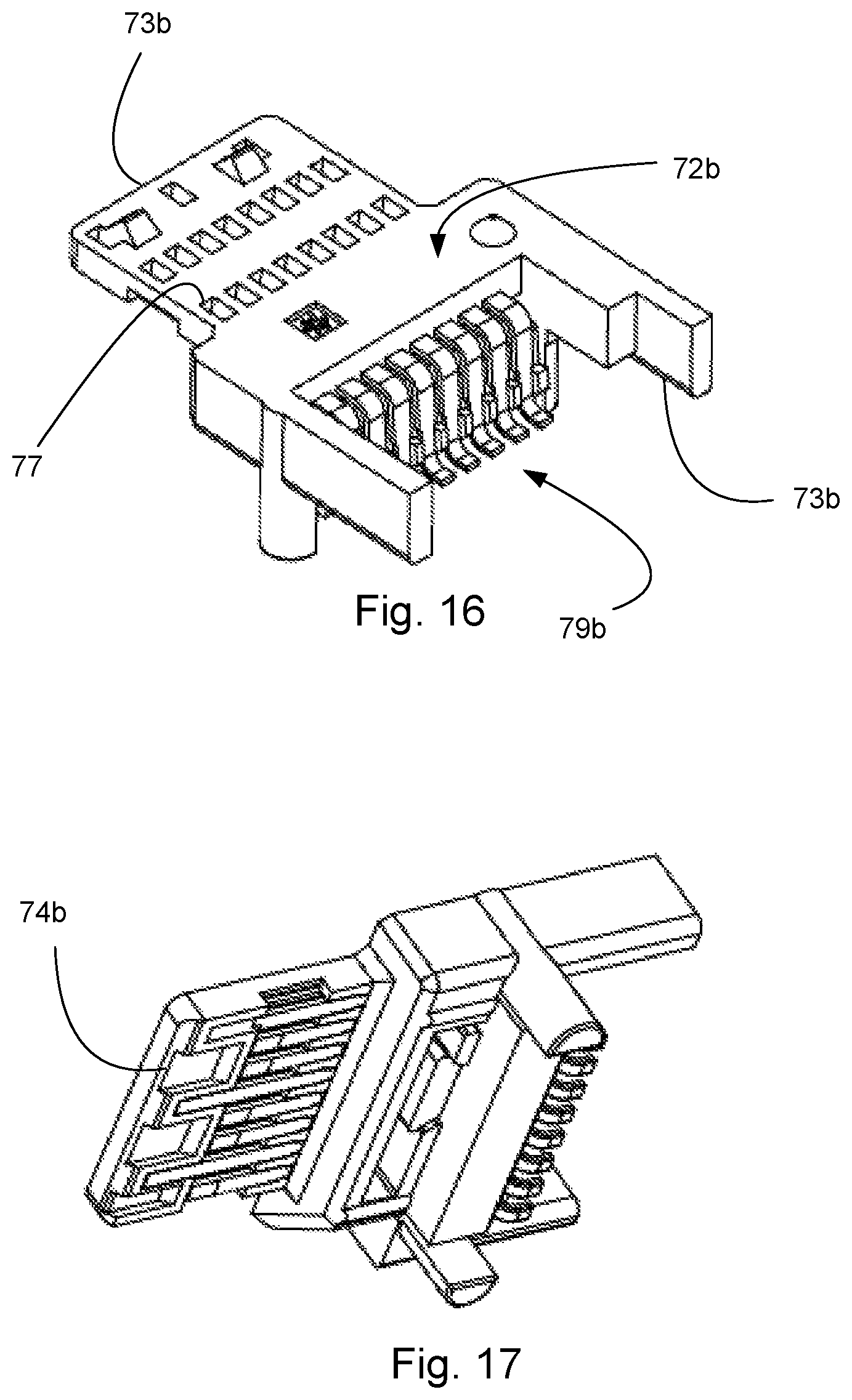
FIG. 16 illustrates a perspective view of an embodiment of a second housing wafer.
FIG. 17 illustrates another perspective view of the embodiment depicted in FIG. 16.
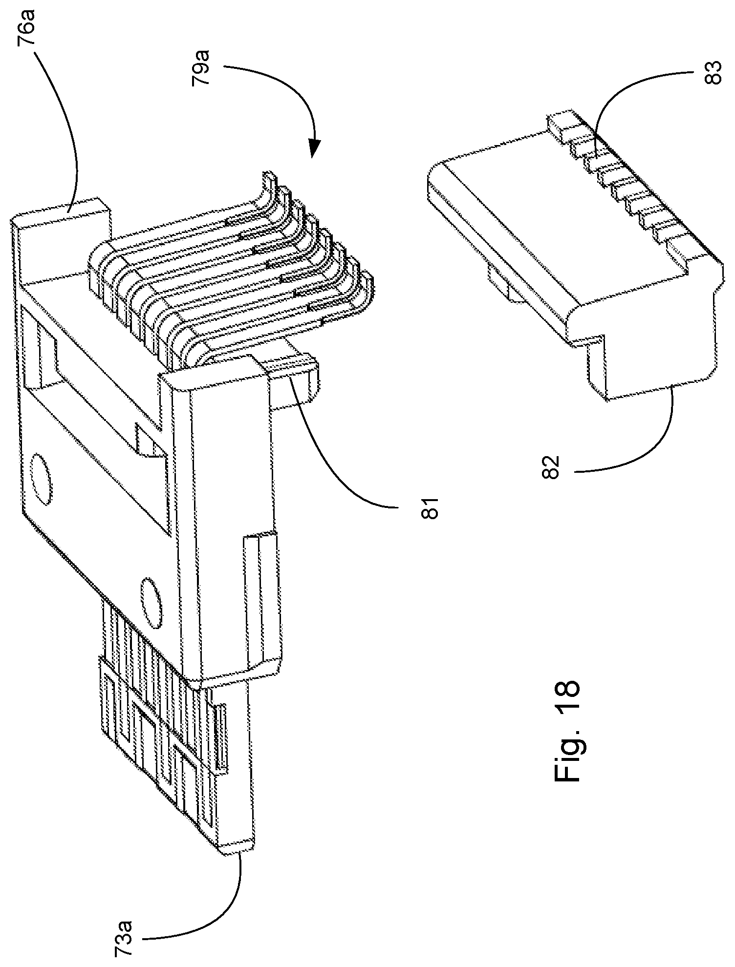
FIG. 18 illustrates a perspective, partially exploded view of an embodiment of a first housing wafer.
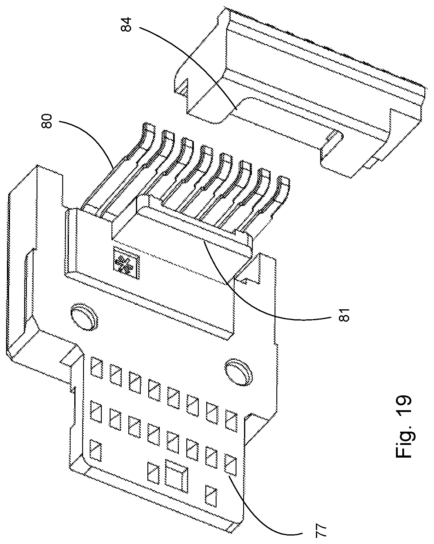
FIG. 19 illustrates another perspective view of the embodiment depicted in FIG. 18.
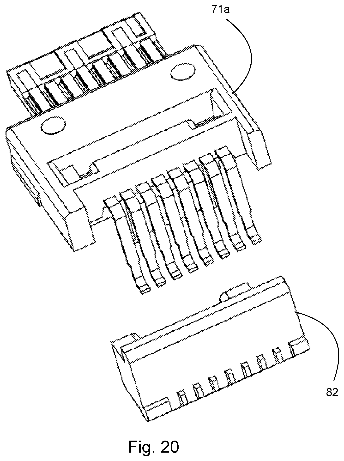
FIG. 20 illustrates another perspective view of the embodiment depicted in FIG. 18.
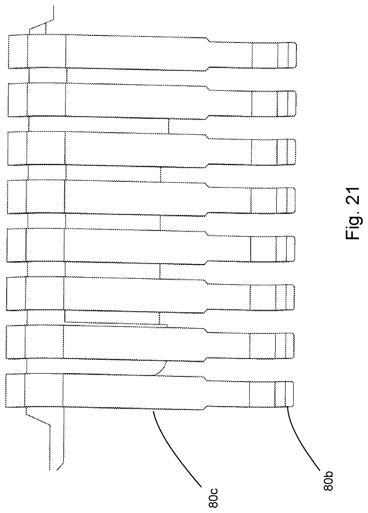
FIG. 21 illustrates an elevated rear view of a portion of an embodiment of a terminal set, showing an embodiment of uniform construction of the terminals.
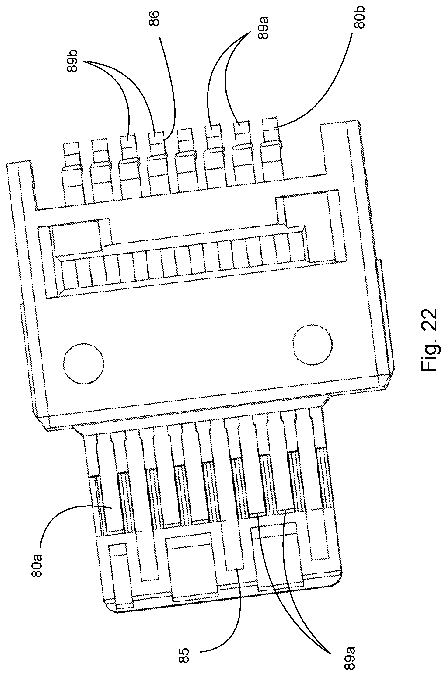
FIG. 22 illustrates a perspective simplified view of an embodiment of a first housing wafer with a terminal block removed.
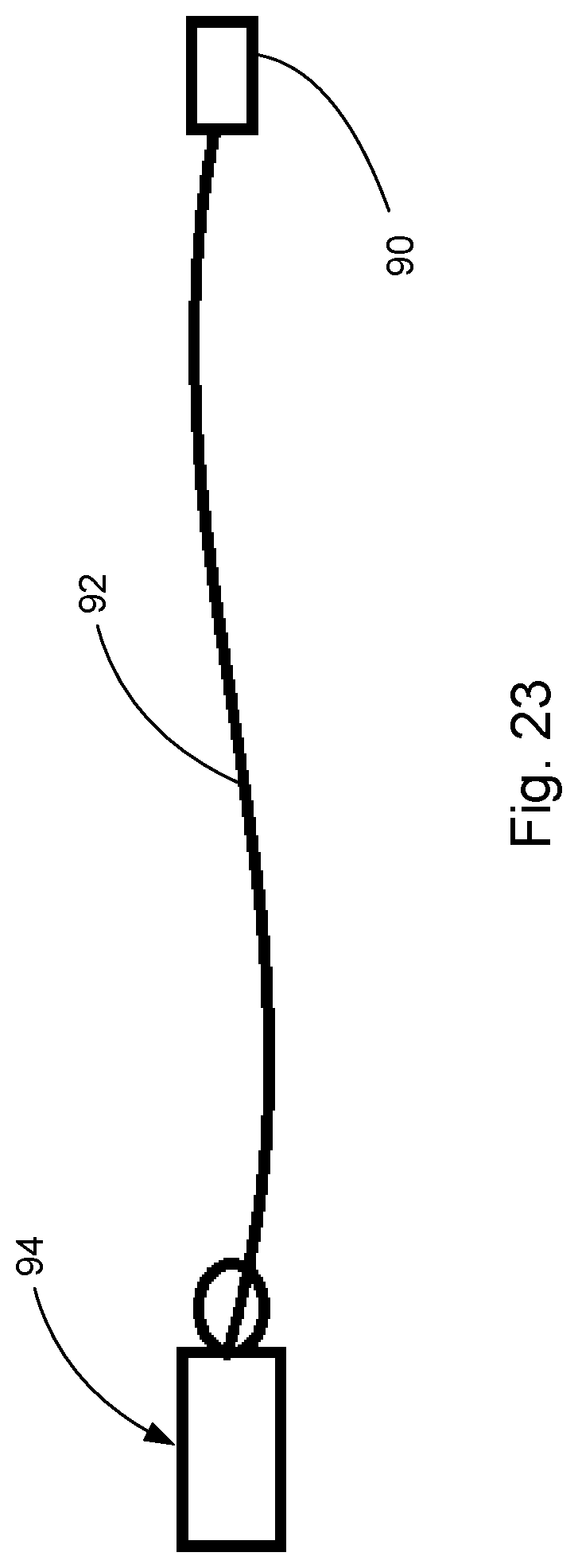
FIG. 23 illustrates a schematic representation of an embodiment of a cable assembly.
DETAILED DESCRIPTION
The detailed description that follows describes exemplary embodiments and is not intended to be limited to the expressly disclosed combination(s), Therefore, unless otherwise noted, features disclosed herein may be combined together to form additional combinations that were not otherwise shown for purposes of brevity.
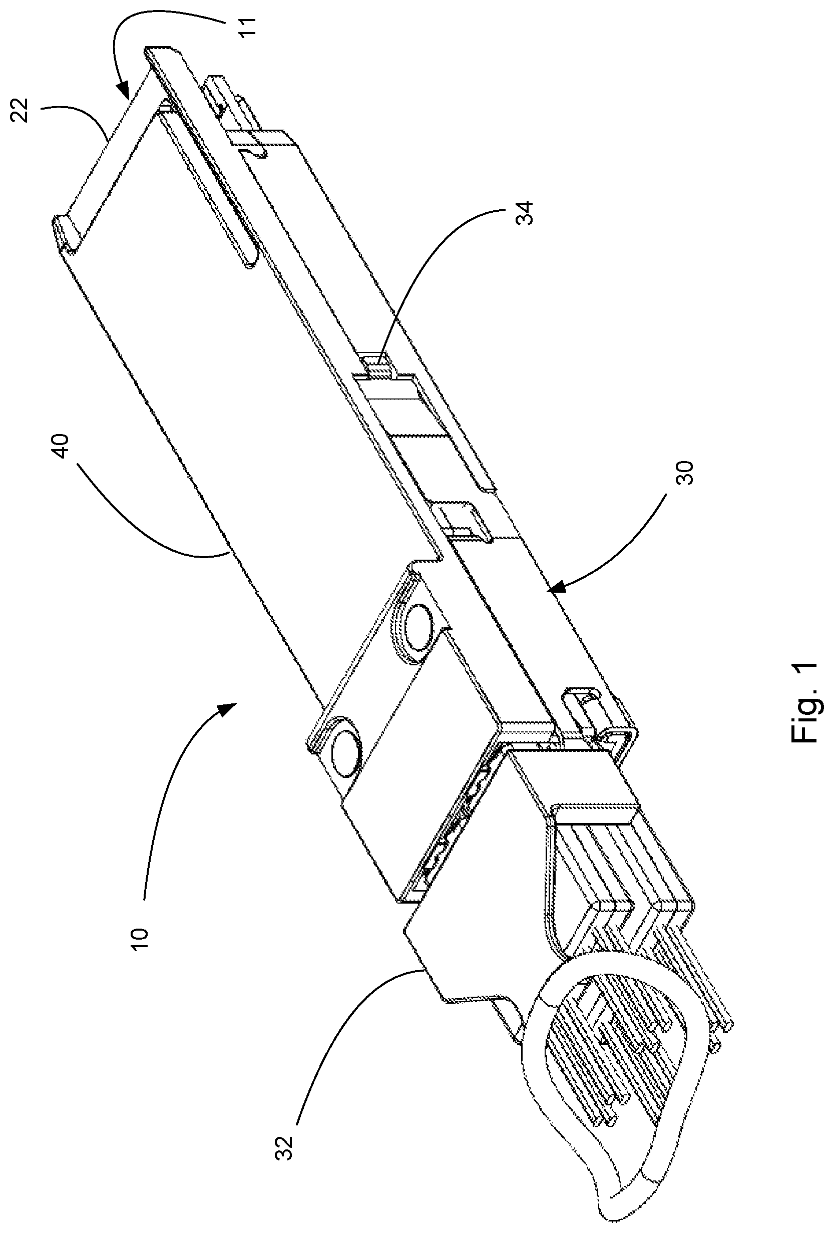
As can be appreciated from the Figures, a plug module 10 is depicted and as depicted can result in a quad small-form factor pluggable (QSFP) module. Thus, the depicted embodiment allows for the insertion of the plug module 10 into an existing QSFP receptacle port and can provide four break out connectors. QSFP modules are fairly beneficial for Top of Rack (ToR) applications as well as many other applications that benefit from 4 channels of high-speed data. The features discussed herein, however, are not limited to use with QSFP style connectors as other sized plug receptacle could also provide similar functionality (with larger plug modules potentially supporting additional connectors).
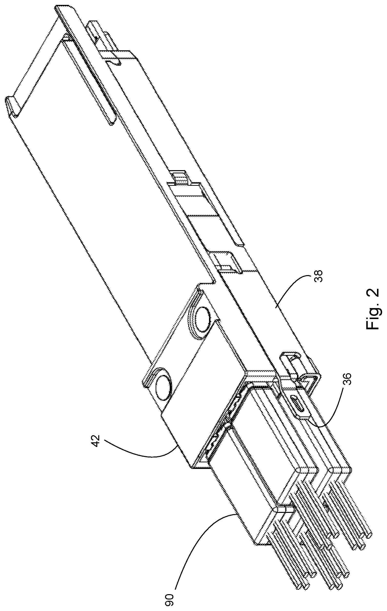
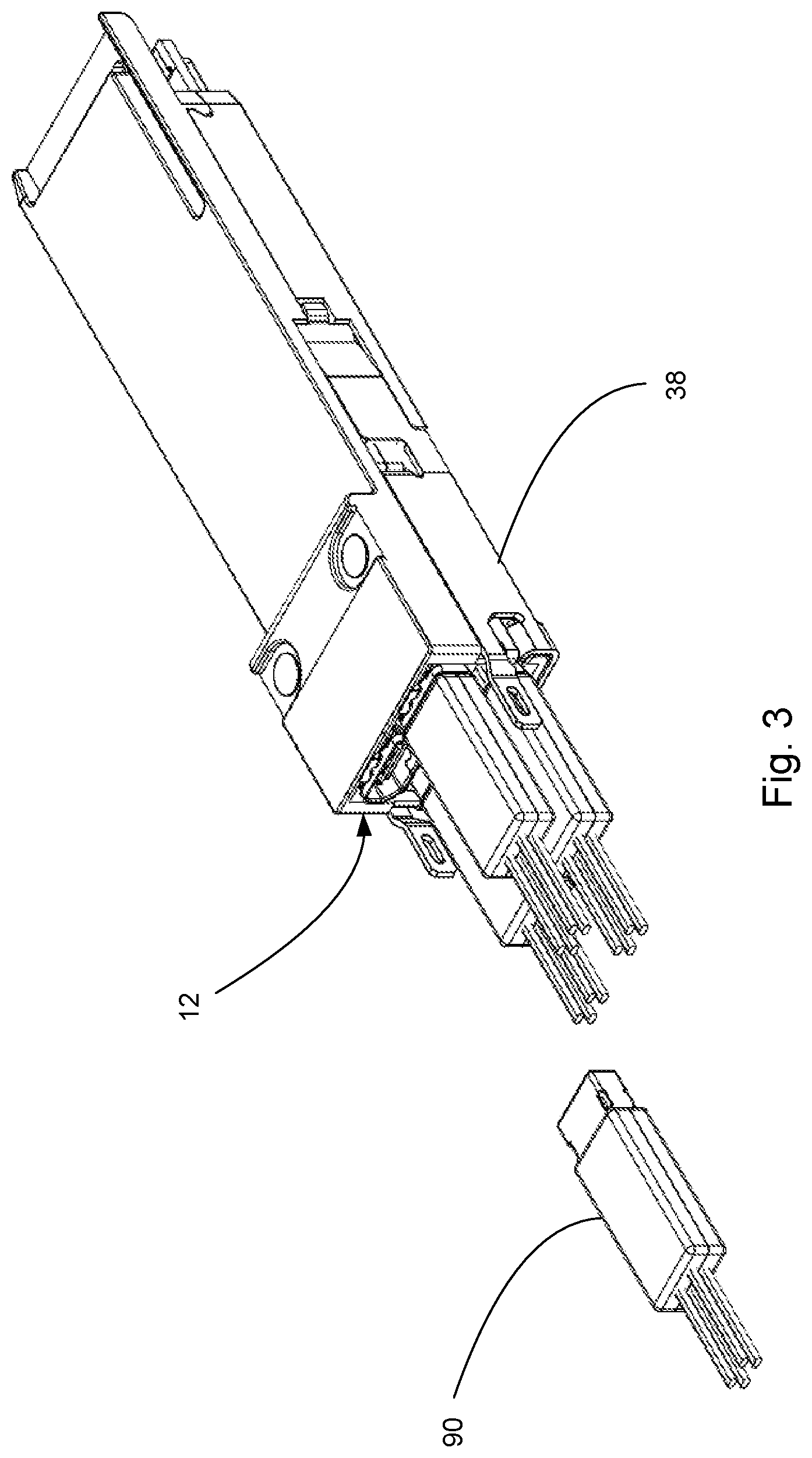
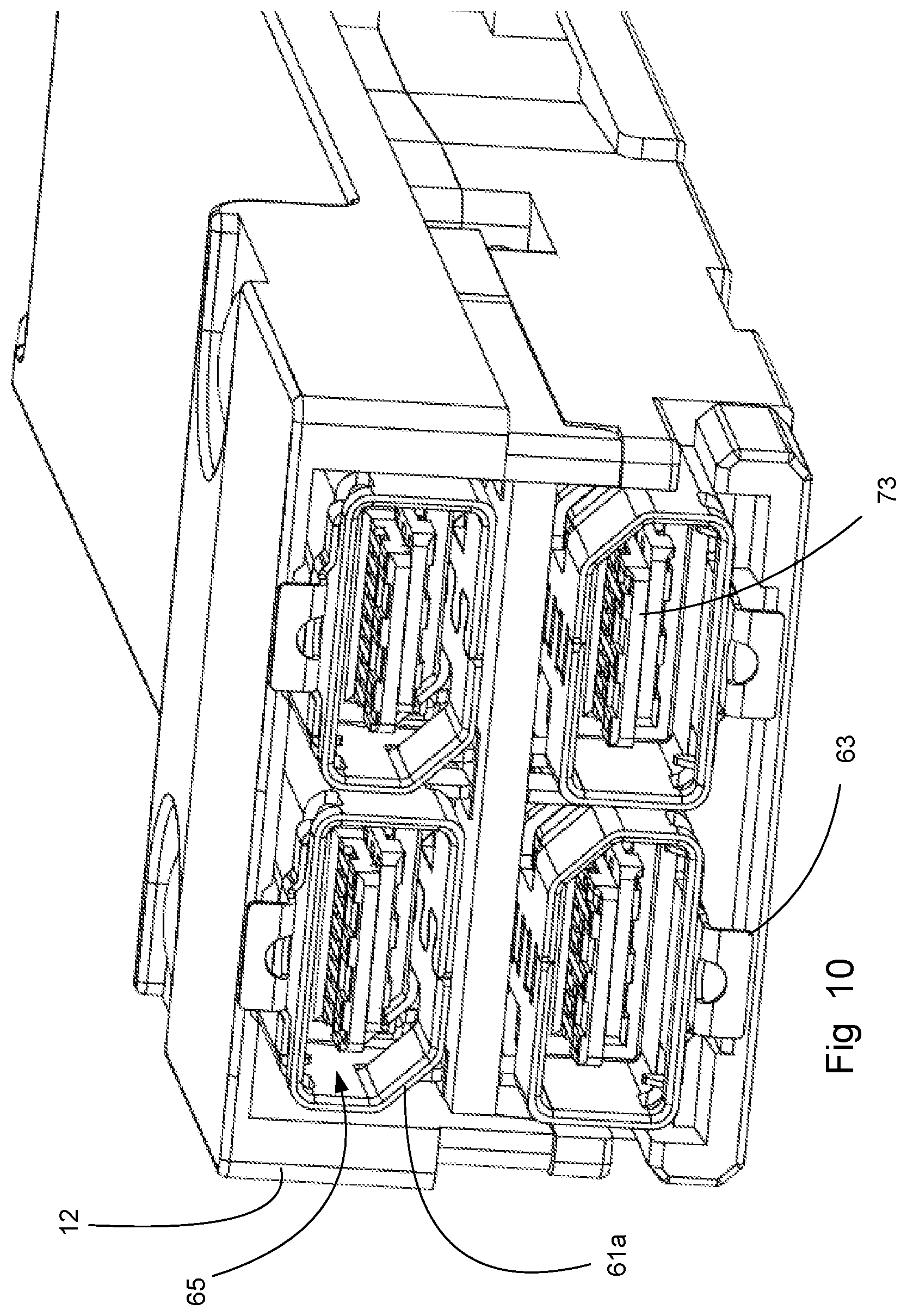
The depicted plug module 10 includes a latch 30 with an optional pull-tab 32 that is removed in FIG. 2. As can be appreciated, the plug module has a body 40 formed of a lower half 43a and an upper half 43b that are secured together with fasteners 44 and the plug module 10 has a first mating end 11 and a second mating end 12 opposing the first mating end 11. In operation, the first mating end 11 is configured to mate with a receptacle (not shown but which could be a standard QSFP receptacle) and the second mating end 12 is intended to provide receptacles as discussed herein.
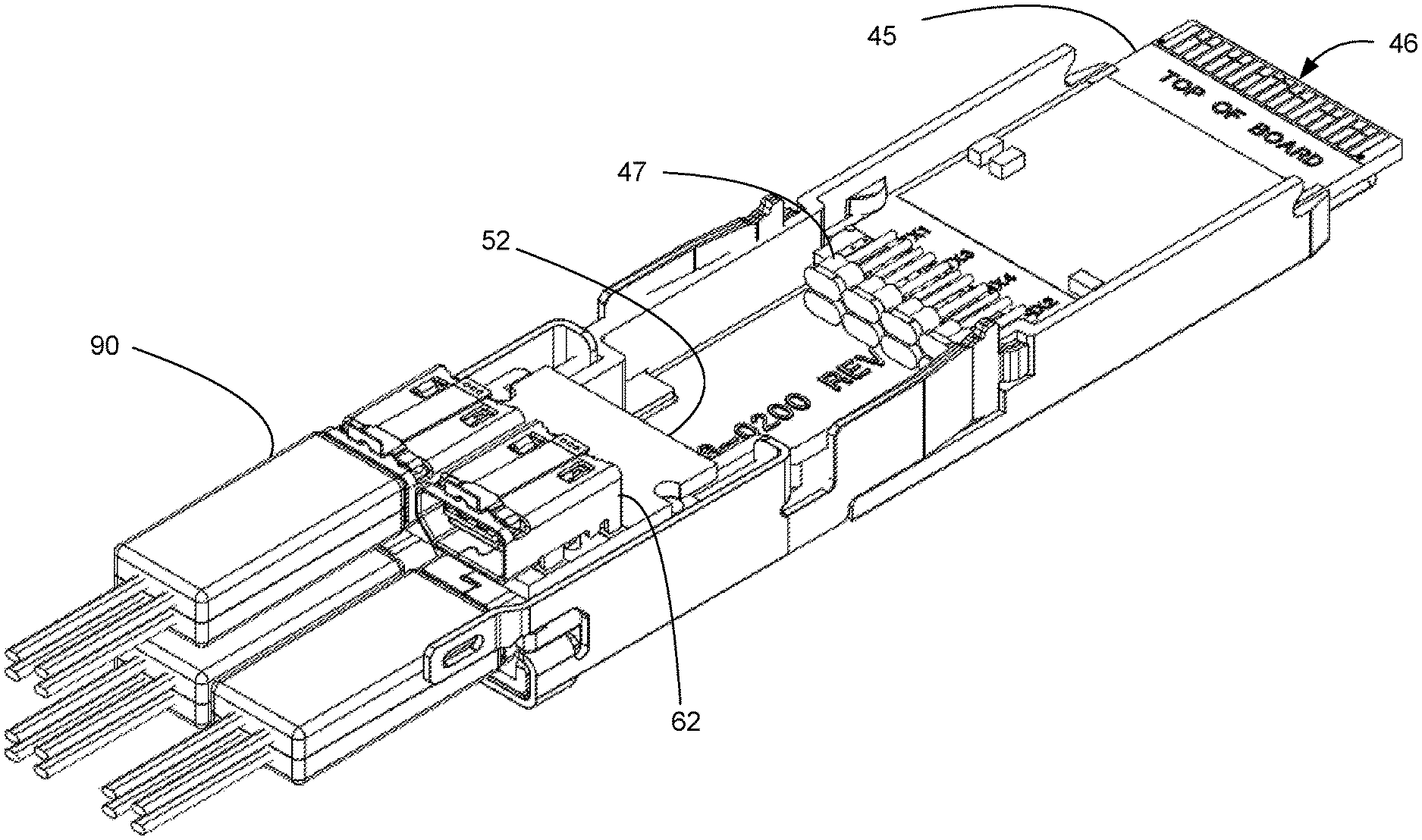
A paddle card 45 with contact pads 46 is provided on a first mating end 11 and the paddle card 45 is configured to mate with a corresponding connector (typically one that includes a card slot). Four micro receptacles 60 are provided at the second mating end 12 and each micro receptacle 60 includes a mating face 61a and a rear face 61b. While such data rates are not required, the micro receptacles 60 mounted in the plug module 10 can each support a two-way 25 Gbps channel with a design that provides one transmit pair and one receive pair (both configured to operate at 25 Gbps using NRZ encoding) with a total of 16 pins while being less than 7 mm wide. It should be noted that the depicted plug module 10 is configured as a QSFP style plug module and thus is intended to mate with a receptacle that supports four two-way channels (e.g., with a 4.times. receptacle) and thus it makes sense to break out the one 4.times. into four 1.times. connectors. Do to size constraints, the micro receptacles 60 have less pins than a typical SFP connector would have but for many applications the 16 pins are sufficient. It should be noted that if the plug module was configured to engage a 2.times. receptacle then two 1.times. connectors would be sufficient from a break out standpoint and the design of the plug module could be so modified.
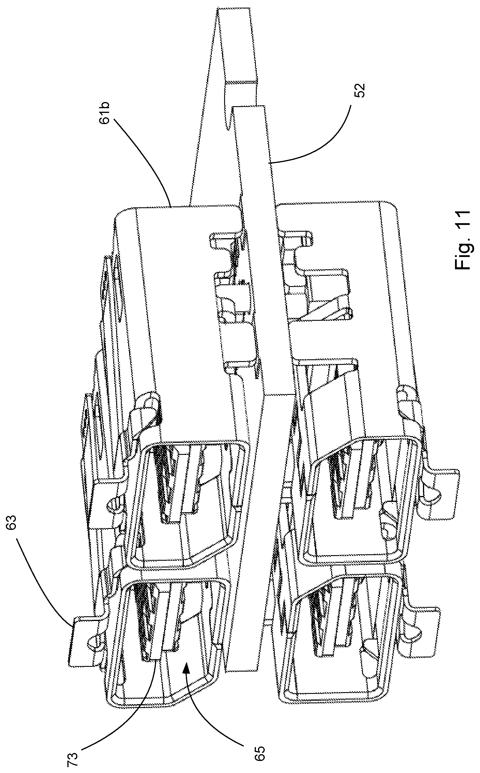
Each micro receptacle 60 is supported on a micro board 52 and includes a cage 62 and a latch 63. The latch 63 ensures that a mating micro plug connector 90 is securely fastened to the micro receptacle 60 and is not going to fall out do to vibration and inadvertent application of force to the micro plug connector 90. It should be noted that the depicted design includes a cable 47 (shown in truncated manner) that connects the paddle card 45 to the micro board 52. For purposes of illustration the termination of the cable 47 to the micro board 52 is omitted as such a termination is known and can be substantially the same as the termination shown on the paddle card 45. As is discussed, such a configuration is not required but it has been determination that such a configuration is desirable because it allows the micro board 52 to be offset upward compared to the paddle card 45. It turns out that offsetting the micro receptacles upward compared to the paddle card 45 is beneficial for users and it can help make it easier to package the plug module in a given system. Alternative embodiments could use flex circuitry to connect the micro receptacles 60 to the paddle card 45 and still provide the offset configuration. Other alternative embodiments that provide the optional offset configuration could include the use of a non-planar circuit board but in general a circuit board tends to be more lossy than a cable so care is needed to ensure the selected configuration is compatible with the signaling frequency and loss budget.
The micro receptacles 60 provide a micro port 65 that is defined by the cage 62 (preferably formed of a metal) that extends around a tongue 73 of a housing 70 that is formed of an insulative material. The housing 70 supports the terminals 80. In an embodiment the housing can be formed of a first wafer housing 71a and a second wafer housing 71b, where the first and second water housings 71a, 71b are each insert molded around a row of terminals such that corresponding contacts 80a are supported on a first tongue half 73a and a second tongue half 73b.
As can be appreciated, the micro receptacles 60 are configured as right-angle SMT style connectors with terminal sets 68 that each provide a row of terminals and are intended to be mounted on a pad array 54 on the micro board 52. In an embodiment the terminal sets 68 can have terminals 80 on a 0.5 mm pitch. Each of the terminals 80 includes a contact 80a, a tail 80b and a body 80c that extend therebetween. As can be appreciated, the tails 80b can be provided in two rows. Naturally, the mating micro plug connector 90 has mating terminals that are also arranged at a 0.5 mm pitch. In spite of the small size, the far end crosstalk can be more than 35 dB down and preferably can be more than 40 dB down out to 12.5 GHz signaling frequency.
To help provide the desirable performance, one of the rows of terminals can include signal terminals 86 (that form differential signal pairs 89a, 89b) spaced apart by a ground terminal 85 and in an embodiment the tongue and contact configuration can be adjusted so that the ground terminals 85 extends past the signal terminals 86 and notches 74a, 74b are provided in the first and second tongue halves 73a, 73b where the corresponding notch is placed at the end of the signal terminals 86 that form the differential pair. While such an optional configuration is not required, it has been determined that for a compact design as depicted it is beneficial to have the notches 74a, 74b as depicted so as to improve the tuning of the terminals. The notches 74a, 74b, in combination with tuning apertures 77, can be arranged so that the signal terminals are preferentially coupled (e.g., more signal energy travels on the signal terminals than would normally travel on a symmetric configuration). This can be done by modifying the dielectric constant of the structure surrounding the signal terminals so that they are more tightly coupled together than one of the signal terminals is coupled to an adjacent ground terminal. As can be appreciated from FIG. 21, however, in an embodiment the spacing and construction of the terminals can be symmetric in that the space between ground and signal terminals, along with the shape of the terminals, is substantially the same along the body and tail sections.
As depicted, the first wafer half 71a includes a terminal block 82 that attaches to a projection 81 via a receiving channel 84. The terminal block 82, while it can be integrated into the first wafer half 71a, is preferably separate and provides a terminal comb 83 that helps control the location and spacing of the tails. The second wafer half 71b can be an integral unit, as is depicted.
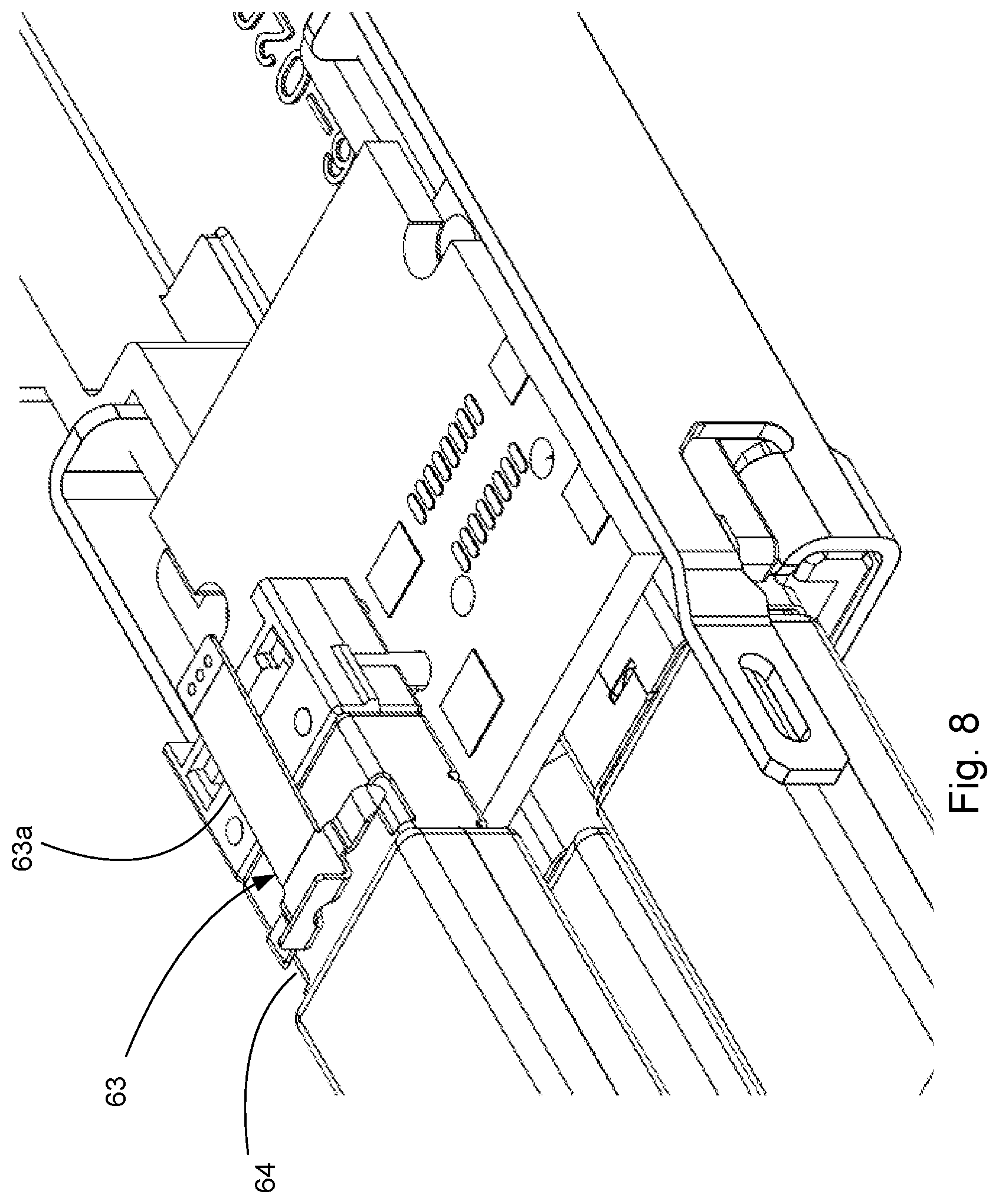
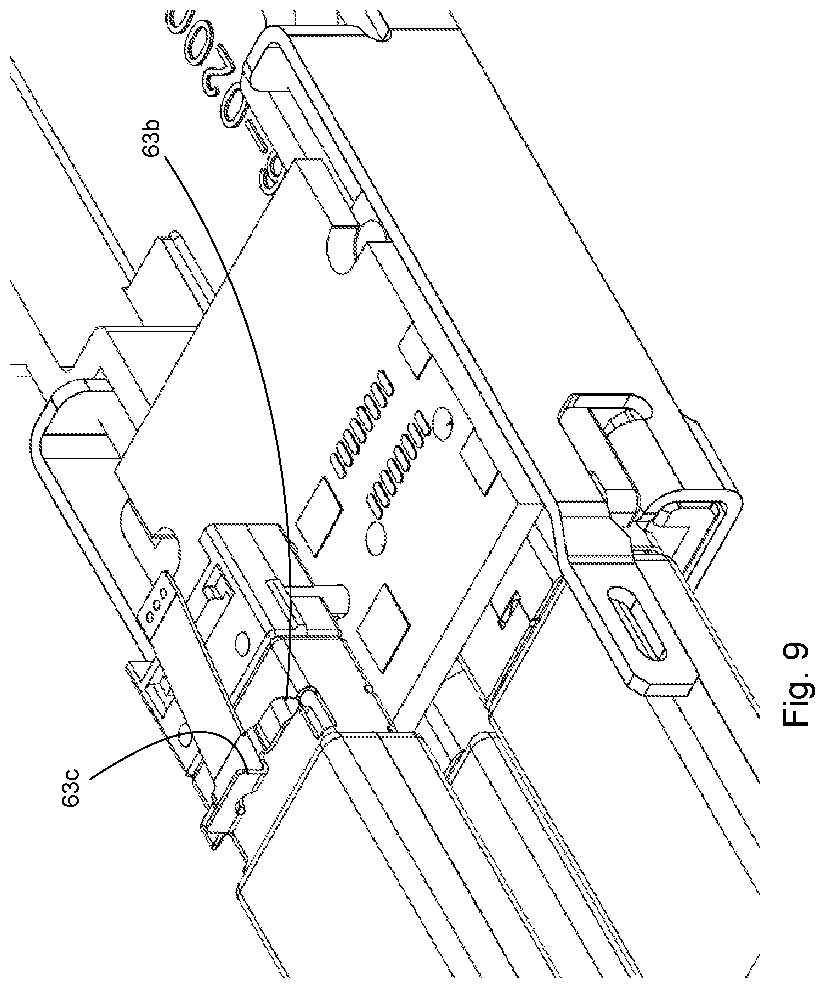
One issue that exists is the inclusion of the latch 63. As can be appreciated, there is very little space available and a latch that could be operated without a tool would be difficult to package. For certain applications a latch may not be required. However, for server applications and any applications where there is a need for a robust configuration that is resistant to accidental disengagement of a connector, a latch is needed. While it is common to place the latch on the plug module, the micro plug modules are so small and the space is so tight when they are arranged as depicted that providing a latch on the micro plugs is not feasible. As a result, Applicants have determined that the latch 63 can be provided on the micro receptacle 60.
The depicted system therefore includes an optional latch 63 that is configured to retain a micro plug module that is inserted into the micro receptacle. The latch 63 includes a securing arm 63a that has one end secured to the cage 62 of the micro receptacle 60 and has retaining fingers 63b that extend through retaining apertures 64 in the cage 62 so that the retaining fingers 63b can engage the inserted plug connector and a release flange 63c is moveable with the use of a tool. In operation a tool can be inserted under the release flange 63c so as to cause the securing arm 63a to be translated upward. This will cause retaining fingers 63b on the securing arm 63a to disengage from retaining holes in the micro plug and the micro plug can then be removed. The translation of the securing arm 63a can be appreciated from the embodiments depicted in FIGS. 8 and 9. Naturally, if it is desirable to remove several micro plugs from a plug module 10 then it may be easier to first disconnect the plug module first and then remove the micro plugs.
As noted above, the micro receptacles 60 are mounted on a micro board 52. As depicted, the micro board 52 is separate from the paddle card 45. In an alternative embodiment the paddle card could be extended so that the micro board 52 and the paddle card 45 were integral or a single board and the micro receptacles 60 could be mounted directly on the paddle card 45 (and thus communicate via traces provided on the paddle card 45). Otherwise the micro board 52 and the paddle card 45 can be connected together in any desirable manner. It should be noted that if desired the plug module could also include circuitry such as a retimer and/or an amplifier to allow for improved operation.
While active components can be added, it should be noted that the depicted configuration is intended to work as a passive system in certain applications. This is beneficial because the micro plug modules can be mounted on a cable assembly that has a different style connector on the opposite end. Thus the micro plug connector 90 could be provided on one end of a cable 92 and a conventional SFP style plug 94 could be placed on the other end (such as is depicted schematically in FIG. 23).
The disclosure provided herein describes features in terms of preferred and exemplary embodiments thereof. Numerous other embodiments, modifications and variations within the scope and spirit of the appended claims will occur to persons of ordinary skill in the art from a review of this disclosure.
* * * * *
D00000
D00001
D00002
D00003
D00004
D00005
D00006
D00007
D00008
D00009
D00010
D00011
D00012
D00013
D00014
D00015
D00016
D00017
D00018
D00019
D00020
D00021
XML
uspto.report is an independent third-party trademark research tool that is not affiliated, endorsed, or sponsored by the United States Patent and Trademark Office (USPTO) or any other governmental organization. The information provided by uspto.report is based on publicly available data at the time of writing and is intended for informational purposes only.
While we strive to provide accurate and up-to-date information, we do not guarantee the accuracy, completeness, reliability, or suitability of the information displayed on this site. The use of this site is at your own risk. Any reliance you place on such information is therefore strictly at your own risk.
All official trademark data, including owner information, should be verified by visiting the official USPTO website at www.uspto.gov. This site is not intended to replace professional legal advice and should not be used as a substitute for consulting with a legal professional who is knowledgeable about trademark law.