Method of encapsulating an environmentally sensitive device
Chu , et al. March 16, 2
U.S. patent number 10,950,821 [Application Number 16/717,261] was granted by the patent office on 2021-03-16 for method of encapsulating an environmentally sensitive device. This patent grant is currently assigned to Samsung Display Co., Ltd.. The grantee listed for this patent is Samsung Display Co., Ltd.. Invention is credited to Xi Chu, Gordon L. Graff, Steve Shi Lin.


| United States Patent | 10,950,821 |
| Chu , et al. | March 16, 2021 |
Method of encapsulating an environmentally sensitive device
Abstract
Methods of encapsulating an environmentally sensitive device. The methods involve temporarily laminating a flexible substrate to a rigid support using a reversible adhesive for processing, reversing the reversible adhesive, and removing the device from the rigid support.
| Inventors: | Chu; Xi (Freemont, CA), Lin; Steve Shi (Sunnyvale, CA), Graff; Gordon L. (West Richland, WA) | ||||||||||
|---|---|---|---|---|---|---|---|---|---|---|---|
| Applicant: |
|
||||||||||
| Assignee: | Samsung Display Co., Ltd.
(Yongin, KR) |
||||||||||
| Family ID: | 1000005426474 | ||||||||||
| Appl. No.: | 16/717,261 | ||||||||||
| Filed: | December 17, 2019 |
Prior Publication Data
| Document Identifier | Publication Date | |
|---|---|---|
| US 20200119309 A1 | Apr 16, 2020 | |
Related U.S. Patent Documents
| Application Number | Filing Date | Patent Number | Issue Date | ||
|---|---|---|---|---|---|
| 14669216 | Mar 26, 2015 | ||||
| 11627602 | Jan 26, 2007 | ||||
| Current U.S. Class: | 1/1 |
| Current CPC Class: | H01L 51/0024 (20130101); B32B 37/0076 (20130101); B32B 37/02 (20130101); H01L 21/568 (20130101); B32B 37/1207 (20130101); H01L 51/5256 (20130101); H01L 51/448 (20130101); B32B 38/0004 (20130101); B32B 38/10 (20130101); H01L 51/107 (20130101); B32B 2307/7244 (20130101); H01L 2251/566 (20130101); B32B 2307/546 (20130101); B32B 2037/246 (20130101); B32B 2457/00 (20130101); Y10T 428/239 (20150115); B32B 2307/7246 (20130101); H01L 2227/326 (20130101); H01L 2251/5338 (20130101); Y02E 10/549 (20130101) |
| Current International Class: | H01L 51/52 (20060101); H01L 51/10 (20060101); H01L 51/00 (20060101); H01L 51/44 (20060101); B32B 38/10 (20060101); B32B 38/00 (20060101); H01L 21/56 (20060101); B32B 37/00 (20060101); B32B 37/02 (20060101); B32B 37/12 (20060101); B32B 37/24 (20060101) |
References Cited [Referenced By]
U.S. Patent Documents
| 2382432 | August 1945 | McManus et al. |
| 2384500 | September 1945 | Stoll |
| 3475307 | October 1969 | Knox et al. |
| 3496427 | February 1970 | Lee |
| 3607365 | September 1971 | Lindlof |
| 3661117 | May 1972 | Cornelius et al. |
| 3941630 | March 1976 | Larrabee |
| 4061835 | December 1977 | Poppe et al. |
| 4098965 | July 1978 | Kinsman |
| 4266223 | May 1981 | Frame |
| 4283482 | August 1981 | Hattori et al. |
| 4313254 | February 1982 | Feldman et al. |
| 4426275 | January 1984 | Meckel et al. |
| 4521458 | June 1985 | Nelson |
| 4537814 | August 1985 | Itoh et al. |
| 4555274 | November 1985 | Kitajima et al. |
| 4557978 | December 1985 | Mason |
| 4572845 | February 1986 | Christen |
| 4581337 | April 1986 | Frey et al. |
| 4624867 | November 1986 | Iijima et al. |
| 4690728 | September 1987 | Tsang et al. |
| 4695618 | September 1987 | Mowrer |
| 4710426 | December 1987 | Stephens |
| 4722515 | February 1988 | Ham |
| 4768666 | September 1988 | Kessler |
| 4842893 | June 1989 | Yializis et al. |
| 4843036 | June 1989 | Schmidt et al. |
| 4855186 | August 1989 | Grolig et al. |
| 4889609 | December 1989 | Cannella |
| 4913090 | April 1990 | Harada et al. |
| 4931158 | June 1990 | Bunshah et al. |
| 4934315 | June 1990 | Linnebach et al. |
| 4954371 | September 1990 | Yializis |
| 4977013 | December 1990 | Ritchie et al. |
| 5032461 | July 1991 | Shaw et al. |
| 5036249 | July 1991 | Pike-Biegunski et al. |
| 5047131 | September 1991 | Wolfe et al. |
| 5059861 | October 1991 | Littman et al. |
| 5124204 | June 1992 | Yamashita et al. |
| 5189405 | February 1993 | Yamashita et al. |
| 5203898 | April 1993 | Carpenter et al. |
| 5204314 | April 1993 | Kirlin et al. |
| 5237439 | August 1993 | Misono et al. |
| 5260095 | November 1993 | Affinito |
| 5336324 | August 1994 | Stall et al. |
| 5344501 | September 1994 | Hashimoto et al. |
| 5354497 | October 1994 | Fukuchi et al. |
| 5356947 | October 1994 | Ali et al. |
| 5357063 | October 1994 | House et al. |
| 5376467 | December 1994 | Abe et al. |
| 5393607 | February 1995 | Kawasaki et al. |
| 5395644 | March 1995 | Affinito |
| 5402314 | March 1995 | Amago et al. |
| 5427638 | June 1995 | Goetz et al. |
| 5440446 | August 1995 | Shaw et al. |
| 5451449 | September 1995 | Shetty et al. |
| 5461545 | October 1995 | Leroy et al. |
| 5464667 | November 1995 | Koehler et al. |
| 5510173 | April 1996 | Pass et al. |
| 5512320 | April 1996 | Turner et al. |
| 5536323 | July 1996 | Kirlin et al. |
| 5547508 | August 1996 | Affinito |
| 5554220 | September 1996 | Forrest et al. |
| 5576101 | November 1996 | Saitoh et al. |
| 5578141 | November 1996 | Mori et al. |
| 5607789 | March 1997 | Treger et al. |
| 5620524 | April 1997 | Fan et al. |
| 5629389 | May 1997 | Roitman et al. |
| 5652192 | July 1997 | Matson et al. |
| 5654084 | August 1997 | Egert |
| 5660961 | August 1997 | Yu |
| 5665280 | September 1997 | Tropsha |
| 5681615 | October 1997 | Aftinito et al. |
| 5681666 | October 1997 | Treger et al. |
| 5684084 | November 1997 | Lewin et al. |
| 5686360 | November 1997 | Harvey, III et al. |
| 5693956 | December 1997 | Shi et al. |
| 5695564 | December 1997 | Imahashi |
| 5711816 | January 1998 | Kirlin et al. |
| 5725909 | March 1998 | Shaw et al. |
| 5731661 | March 1998 | So et al. |
| 5736207 | April 1998 | Walther et al. |
| 5747182 | May 1998 | Friend et al. |
| 5757126 | May 1998 | Harvey, III et al. |
| 5759329 | June 1998 | Krause et al. |
| 5771177 | June 1998 | Tada et al. |
| 5771562 | June 1998 | Harvey, III et al. |
| 5782355 | July 1998 | Katagiri et al. |
| 5792550 | August 1998 | Phillips et al. |
| 5795399 | August 1998 | Hasegawa et al. |
| 5811177 | September 1998 | Shi et al. |
| 5811183 | September 1998 | Shaw et al. |
| 5821138 | October 1998 | Yamazaki et al. |
| 5821692 | October 1998 | Rogers et al. |
| 5844363 | December 1998 | Gu et al. |
| 5861658 | January 1999 | Cronin et al. |
| 5869791 | February 1999 | Young |
| 5872355 | February 1999 | Hueschen |
| 5891554 | April 1999 | Hosokawa et al. |
| 5895228 | April 1999 | Biebuyck et al. |
| 5902641 | May 1999 | Affinito et al. |
| 5902688 | May 1999 | Antoniadis et al. |
| 5904958 | May 1999 | Dick et al. |
| 5912069 | June 1999 | Yializis et al. |
| 5919328 | July 1999 | Tropsha et al. |
| 5920080 | July 1999 | Jones |
| 5922161 | July 1999 | Wu et al. |
| 5929562 | July 1999 | Pichler |
| 5934856 | August 1999 | Asakawa et al. |
| 5945174 | August 1999 | Shaw et al. |
| 5948552 | September 1999 | Antoniadis et al. |
| 5952778 | September 1999 | Haskal et al. |
| 5955161 | September 1999 | Tropsha |
| 5965907 | October 1999 | Huang et al. |
| 5968620 | October 1999 | Harvey et al. |
| 5994174 | November 1999 | Carey et al. |
| 5996498 | December 1999 | Lewis |
| 6004660 | December 1999 | Topolski et al. |
| 6013337 | January 2000 | Knors |
| 6040017 | March 2000 | Mikhael et al. |
| 6045864 | April 2000 | Lyons et al. |
| 6066826 | May 2000 | Yializis |
| 6083313 | July 2000 | Venkatraman et al. |
| 6083628 | July 2000 | Yializis |
| 6084702 | July 2000 | Byker et al. |
| 6087007 | July 2000 | Fujii et al. |
| 6092269 | July 2000 | Yializis et al. |
| 6106627 | August 2000 | Yializis |
| 6117266 | September 2000 | Horzel et al. |
| 6118218 | September 2000 | Yializis et al. |
| 6137221 | October 2000 | Roitman et al. |
| 6146225 | November 2000 | Sheats et al. |
| 6146462 | November 2000 | Yializis et al. |
| 6150187 | November 2000 | Zyung et al. |
| 6165566 | December 2000 | Tropsha |
| 6178082 | January 2001 | Farooq et al. |
| 6195142 | February 2001 | Gyotoku et al. |
| 6198217 | March 2001 | Suzuki et al. |
| 6198220 | March 2001 | Jones et al. |
| 6203898 | March 2001 | Kohler et al. |
| 6207238 | March 2001 | Affinito |
| 6207239 | March 2001 | Affinito |
| 6214422 | April 2001 | Yializis |
| 6217947 | April 2001 | Affinito |
| 6224948 | May 2001 | Affinito |
| 6228434 | May 2001 | Affinito |
| 6228436 | May 2001 | Affinito |
| 6231939 | May 2001 | Shaw et al. |
| 6264747 | July 2001 | Shaw et al. |
| 6268695 | July 2001 | Affinito |
| 6274204 | August 2001 | Affinito |
| 6322860 | November 2001 | Stein et al. |
| 6333065 | December 2001 | Arai et al. |
| 6348237 | February 2002 | Kohler et al. |
| 6350034 | February 2002 | Fleming et al. |
| 6352777 | March 2002 | Bulovic et al. |
| 6358570 | March 2002 | Affinito |
| 6361885 | March 2002 | Chou |
| 6387732 | May 2002 | Akram |
| 6397776 | June 2002 | Yang et al. |
| 6413645 | July 2002 | Graff et al. |
| 6416872 | July 2002 | Maschwitz |
| 6420003 | July 2002 | Shaw et al. |
| 6436544 | August 2002 | Veyrat et al. |
| 6460369 | October 2002 | Hosokawa |
| 6465953 | October 2002 | Duggal |
| 6468595 | October 2002 | Mikhael et al. |
| 6469437 | October 2002 | Parthasarathy et al. |
| 6469438 | October 2002 | Fukuoka et al. |
| 6492026 | December 2002 | Graff et al. |
| 6495953 | December 2002 | Imura |
| 6497598 | December 2002 | Affinito |
| 6497924 | December 2002 | Affinito et al. |
| 6509065 | January 2003 | Affinito |
| 6512561 | January 2003 | Terashita et al. |
| 6522067 | February 2003 | Graff et al. |
| 6537688 | March 2003 | Silvernail et al. |
| 6544600 | April 2003 | Affinito et al. |
| 6548912 | April 2003 | Graff et al. |
| 6569515 | May 2003 | Hebrink et al. |
| 6570325 | May 2003 | Graff et al. |
| 6570714 | May 2003 | Soane et al. |
| 6573652 | June 2003 | Graff et al. |
| 6576351 | June 2003 | Silvernail |
| 6592969 | July 2003 | Burroughes et al. |
| 6597111 | July 2003 | Silvernail et al. |
| 6613395 | September 2003 | Affinito et al. |
| 6614057 | September 2003 | Silvernail et al. |
| 6624568 | September 2003 | Silvernail |
| 6627267 | September 2003 | Aftinito |
| 6628071 | September 2003 | Su |
| 6653780 | November 2003 | Sugimoto et al. |
| 6656537 | December 2003 | Affinito et al. |
| 6660409 | December 2003 | Komatsu et al. |
| 6664137 | December 2003 | Weaver |
| 6681716 | January 2004 | Schaepkens |
| 6710542 | March 2004 | Chun et al. |
| 6720203 | April 2004 | Carcia et al. |
| 6734625 | May 2004 | Vong et al. |
| 6737753 | May 2004 | Kumar et al. |
| 6743524 | June 2004 | Schaepkens |
| 6749940 | June 2004 | Terasaki et al. |
| 6765351 | July 2004 | Forrest et al. |
| 6803245 | October 2004 | Auch et al. |
| 6811829 | November 2004 | Affinito et al. |
| 6815887 | November 2004 | Lee et al. |
| 6818291 | November 2004 | Funkenbusch et al. |
| 6822391 | November 2004 | Yamazaki et al. |
| 6827788 | December 2004 | Takahashi |
| 6835950 | December 2004 | Brown et al. |
| 6836070 | December 2004 | Chung et al. |
| 6837950 | January 2005 | Berard |
| 6852356 | February 2005 | Nishikawa |
| 6864629 | March 2005 | Miyaguchi et al. |
| 6866901 | March 2005 | Burrows et al. |
| 6867539 | March 2005 | McCormick et al. |
| 6872114 | March 2005 | Chung et al. |
| 6872248 | March 2005 | Mizutani et al. |
| 6872428 | March 2005 | Yang et al. |
| 6878467 | April 2005 | Chung et al. |
| 6888305 | May 2005 | Weaver |
| 6888307 | May 2005 | Silvernail et al. |
| 6891330 | May 2005 | Duggal et al. |
| 6897474 | May 2005 | Brown et al. |
| 6897607 | May 2005 | Sugimoto et al. |
| 6902905 | June 2005 | Burson et al. |
| 6905769 | June 2005 | Komada |
| 6911667 | June 2005 | Pichler et al. |
| 6923702 | August 2005 | Graff et al. |
| 6936131 | August 2005 | McCormick et al. |
| 6975067 | December 2005 | McCormick et al. |
| 6994933 | February 2006 | Bates |
| 6998648 | February 2006 | Silvernail |
| 7002294 | February 2006 | Forrest et al. |
| 7012363 | March 2006 | Weaver et al. |
| 7015640 | March 2006 | Schaepkens et al. |
| 7018713 | March 2006 | Padiyath et al. |
| 7029765 | April 2006 | Kwong et al. |
| 7033850 | April 2006 | Tyan et al. |
| 7056584 | June 2006 | Iacovangelo |
| 7074501 | July 2006 | Czeremuszkin et al. |
| 7086918 | August 2006 | Hsiao et al. |
| 7112351 | September 2006 | Affinito |
| 7122418 | October 2006 | Su et al. |
| 7156942 | January 2007 | McCormick et al. |
| 7166007 | January 2007 | Auch et al. |
| 7183197 | February 2007 | Won et al. |
| 7186465 | March 2007 | Bright |
| 7198832 | April 2007 | Burrows et al. |
| 7221093 | May 2007 | Auch et al. |
| 7255823 | August 2007 | Guenther et al. |
| 7298072 | November 2007 | Czeremuszkin et al. |
| 7621794 | November 2009 | Lee et al. |
| 2001/0006827 | July 2001 | Yamazaki et al. |
| 2001/0015074 | August 2001 | Hosokawa |
| 2001/0015620 | August 2001 | Affinito |
| 2001/0044035 | November 2001 | Morii |
| 2002/0015818 | February 2002 | Takahashi et al. |
| 2002/0022156 | February 2002 | Bright |
| 2002/0025444 | February 2002 | Hebrink et al. |
| 2002/0068143 | June 2002 | Silvernail et al. |
| 2002/0069826 | June 2002 | Hunt et al. |
| 2002/0102363 | August 2002 | Affinito et al. |
| 2002/0102818 | August 2002 | Sandhu et al. |
| 2002/0125822 | September 2002 | Graff et al. |
| 2002/0139303 | October 2002 | Yamazaki et al. |
| 2002/0140347 | October 2002 | Weaver |
| 2003/0038590 | February 2003 | Silvernail et al. |
| 2003/0045021 | March 2003 | Akai |
| 2003/0085652 | May 2003 | Weaver |
| 2003/0098647 | May 2003 | Silvernail et al. |
| 2003/0117078 | June 2003 | Jang et al. |
| 2003/0124392 | July 2003 | Bright |
| 2003/0127973 | July 2003 | Weaver et al. |
| 2003/0134487 | July 2003 | Breen et al. |
| 2003/0184222 | October 2003 | Nilsson et al. |
| 2003/0197197 | October 2003 | Brown et al. |
| 2003/0205845 | November 2003 | Pichler et al. |
| 2003/0218422 | November 2003 | Park et al. |
| 2003/0235648 | December 2003 | Affmito et al. |
| 2004/0002729 | January 2004 | Zamore |
| 2004/0014265 | January 2004 | Kazlas et al. |
| 2004/0018305 | January 2004 | Pagano et al. |
| 2004/0029334 | February 2004 | Bijker et al. |
| 2004/0031442 | February 2004 | Yamazaki et al. |
| 2004/0046497 | March 2004 | Schaepkens et al. |
| 2004/0071971 | April 2004 | Iacovangelo |
| 2004/0099926 | May 2004 | Yamazaki et al. |
| 2004/0113542 | June 2004 | Hsiao et al. |
| 2004/0115402 | June 2004 | Schaepkens |
| 2004/0115859 | June 2004 | Murayama et al. |
| 2004/0119028 | June 2004 | McCormick et al. |
| 2004/0175512 | September 2004 | Schaepkens |
| 2004/0175580 | September 2004 | Schaepkens |
| 2004/0187999 | September 2004 | Wilkinson et al. |
| 2004/0209090 | October 2004 | Iwanaga |
| 2004/0212759 | October 2004 | Hayashi |
| 2004/0219380 | November 2004 | Naruse et al. |
| 2004/0229051 | November 2004 | Schaepkens et al. |
| 2004/0241454 | December 2004 | Shaw et al. |
| 2004/0263038 | December 2004 | Ribolzi et al. |
| 2005/0003098 | January 2005 | Kohler et al. |
| 2005/0006786 | January 2005 | Sawada |
| 2005/0017633 | January 2005 | Miyadera |
| 2005/0051094 | March 2005 | Schaepkens et al. |
| 2005/0079295 | April 2005 | Schaepkens |
| 2005/0079380 | April 2005 | Iwanaga |
| 2005/0093001 | May 2005 | Liu et al. |
| 2005/0093437 | May 2005 | Ouyang |
| 2005/0094394 | May 2005 | Padiyath et al. |
| 2005/0095422 | May 2005 | Sager et al. |
| 2005/0095736 | May 2005 | Padiyath et al. |
| 2005/0112378 | May 2005 | Naruse et al. |
| 2005/0115603 | June 2005 | Yoshida et al. |
| 2005/0122039 | June 2005 | Satani |
| 2005/0129841 | June 2005 | McCormick et al. |
| 2005/0133781 | June 2005 | Yan et al. |
| 2005/0140291 | June 2005 | Hirakata et al. |
| 2005/0146267 | July 2005 | Lee et al. |
| 2005/0162421 | July 2005 | Yamazaki et al. |
| 2005/0174045 | August 2005 | Lee et al. |
| 2005/0176181 | August 2005 | Burrows et al. |
| 2005/0202646 | September 2005 | Burrows et al. |
| 2005/0212419 | September 2005 | Vazan et al. |
| 2005/0224935 | October 2005 | Schaepkens et al. |
| 2005/0238846 | October 2005 | Arakatsu et al. |
| 2005/0239294 | October 2005 | Rosenblum et al. |
| 2006/0001040 | January 2006 | Kim et al. |
| 2006/0003474 | January 2006 | Tyan et al. |
| 2006/0006799 | January 2006 | Yamazaki et al. |
| 2006/0028128 | February 2006 | Ohkubo |
| 2006/0061272 | March 2006 | McCormick et al. |
| 2006/0062937 | March 2006 | Padiyath et al. |
| 2006/0063015 | March 2006 | McCormick et al. |
| 2006/0132461 | June 2006 | Furukawa et al. |
| 2006/0216951 | September 2006 | Moro et al. |
| 2006/0246811 | November 2006 | Winters et al. |
| 2006/0250084 | November 2006 | Cok et al. |
| 2006/0278333 | December 2006 | Lee et al. |
| 2006/0291034 | December 2006 | Patry et al. |
| 2007/0009674 | January 2007 | Okubo |
| 2007/0049155 | March 2007 | Moro |
| 2007/0059854 | March 2007 | Huang |
| 2007/0164376 | July 2007 | Burrows et al. |
| 2007/0187759 | August 2007 | Lee et al. |
| 2007/0281089 | December 2007 | Heller et al. |
| 2008/0032076 | February 2008 | Dujardin et al. |
| 2009/0258235 | October 2009 | Tateishi |
| 2010/0193468 | August 2010 | Burrows et al. |
| 704297 | Feb 1968 | BE | |||
| 2353506 | May 2000 | CA | |||
| 1647247 | Jul 2005 | CN | |||
| 19603746 | Apr 1997 | DE | |||
| 69615510 | May 2002 | DE | |||
| 468440 | Jan 1992 | EP | |||
| 547550 | Jun 1993 | EP | |||
| 590467 | Apr 1994 | EP | |||
| 611037 | Aug 1994 | EP | |||
| 722787 | Jul 1996 | EP | |||
| 777280 | Jun 1997 | EP | |||
| 777281 | Jun 1997 | EP | |||
| 787824 | Aug 1997 | EP | |||
| 787826 | Aug 1997 | EP | |||
| 915105 | May 1999 | EP | |||
| 916394 | May 1999 | EP | |||
| 931850 | Jul 1999 | EP | |||
| 977469 | Feb 2000 | EP | |||
| 1021070 | Jul 2000 | EP | |||
| 1127381 | Aug 2001 | EP | |||
| 1130420 | Sep 2001 | EP | |||
| 1278244 | Jan 2003 | EP | |||
| 1426813 | Jun 2004 | EP | |||
| 1514317 | Mar 2005 | EP | |||
| 1719808 | Nov 2006 | EP | |||
| 41004440 | Mar 1966 | JP | |||
| 44008515 | Apr 1969 | JP | |||
| 51047678 | Apr 1976 | JP | |||
| 52090972 | Jul 1977 | JP | |||
| 55001587 | Jan 1980 | JP | |||
| 55001587 | Jan 1980 | JP | |||
| 63096895 | Apr 1988 | JP | |||
| 63136316 | Jun 1988 | JP | |||
| 64018441 | Jan 1989 | JP | |||
| 01041067 | Feb 1989 | JP | |||
| 64041192 | Mar 1989 | JP | |||
| 02183230 | Jul 1990 | JP | |||
| 03290375 | Dec 1991 | JP | |||
| 04267097 | Sep 1992 | JP | |||
| 05182759 | Jul 1993 | JP | |||
| 05217158 | Aug 1993 | JP | |||
| 06136159 | May 1994 | JP | |||
| 06158305 | Jun 1994 | JP | |||
| 06196260 | Jul 1994 | JP | |||
| 06223966 | Aug 1994 | JP | |||
| 07074378 | Mar 1995 | JP | |||
| 07147189 | Jun 1995 | JP | |||
| 07192866 | Jul 1995 | JP | |||
| 8-72188 | Mar 1996 | JP | |||
| 08171988 | Jul 1996 | JP | |||
| 08179292 | Jul 1996 | JP | |||
| 08203669 | Aug 1996 | JP | |||
| 8288522 | Nov 1996 | JP | |||
| 8318590 | Dec 1996 | JP | |||
| 08325713 | Dec 1996 | JP | |||
| 09059763 | Mar 1997 | JP | |||
| 09132774 | May 1997 | JP | |||
| 09161967 | Jun 1997 | JP | |||
| 9201897 | Aug 1997 | JP | |||
| 09232553 | Sep 1997 | JP | |||
| 10000725 | Jan 1998 | JP | |||
| 10013083 | Jan 1998 | JP | |||
| 10016150 | Jan 1998 | JP | |||
| 10312883 | Nov 1998 | JP | |||
| 10334744 | Dec 1998 | JP | |||
| 11017106 | Jan 1999 | JP | |||
| 11040344 | Feb 1999 | JP | |||
| 11149826 | Jun 1999 | JP | |||
| 11255923 | Sep 1999 | JP | |||
| 2000058258 | Feb 2000 | JP | |||
| 3183759 | Jul 2001 | JP | |||
| 2002505969 | Feb 2002 | JP | |||
| 2002117973 | Apr 2002 | JP | |||
| 2002151254 | May 2002 | JP | |||
| 2003217845 | Jul 2003 | JP | |||
| 2003282239 | Oct 2003 | JP | |||
| 2003293122 | Oct 2003 | JP | |||
| 2004186685 | Jul 2004 | JP | |||
| 2004294601 | Oct 2004 | JP | |||
| 2004309932 | Nov 2004 | JP | |||
| 2006294780 | Oct 2006 | JP | |||
| 2006330739 | Dec 2006 | JP | |||
| 2008275737 | Nov 2008 | JP | |||
| 5147678 | Feb 2013 | JP | |||
| 5290972 | Sep 2013 | JP | |||
| 5501587 | May 2014 | JP | |||
| 6179644 | Aug 2017 | JP | |||
| 6234186 | Nov 2017 | JP | |||
| 6396895 | Sep 2018 | JP | |||
| 6418441 | Nov 2018 | JP | |||
| 6441192 | Dec 2018 | JP | |||
| 8707848 | Dec 1987 | WO | |||
| 8900337 | Jan 1989 | WO | |||
| 9107519 | May 1991 | WO | |||
| 9510117 | Apr 1995 | WO | |||
| 9623217 | Aug 1996 | WO | |||
| 9704885 | Feb 1997 | WO | |||
| 9716053 | May 1997 | WO | |||
| 9722631 | Jun 1997 | WO | |||
| 9810116 | Mar 1998 | WO | |||
| 9818852 | May 1998 | WO | |||
| 9904612 | Feb 1999 | WO | |||
| 99/16931 | Apr 1999 | WO | |||
| 9916557 | Apr 1999 | WO | |||
| 9933651 | Jul 1999 | WO | |||
| 0026973 | May 2000 | WO | |||
| 0035603 | Jun 2000 | WO | |||
| 0035604 | Jun 2000 | WO | |||
| 0035993 | Jun 2000 | WO | |||
| 0036661 | Jun 2000 | WO | |||
| 0036665 | Jun 2000 | WO | |||
| 0053423 | Sep 2000 | WO | |||
| 0157904 | Aug 2001 | WO | |||
| 01/68360 | Sep 2001 | WO | |||
| 2001/89006 | Nov 2001 | WO | |||
| 0181649 | Nov 2001 | WO | |||
| 0182389 | Nov 2001 | WO | |||
| 0187825 | Nov 2001 | WO | |||
| 0226973 | Apr 2002 | WO | |||
| 02051626 | Jul 2002 | WO | |||
| 02071506 | Sep 2002 | WO | |||
| 0182336 | Dec 2002 | WO | |||
| 03016589 | Feb 2003 | WO | |||
| 03/090260 | Oct 2003 | WO | |||
| 03098716 | Nov 2003 | WO | |||
| 2004016992 | Feb 2004 | WO | |||
| 2004006199 | Mar 2004 | WO | |||
| 04/070840 | Aug 2004 | WO | |||
| 2004089620 | Oct 2004 | WO | |||
| 2004112165 | Dec 2004 | WO | |||
| 05/015655 | Feb 2005 | WO | |||
| 2005045947 | May 2005 | WO | |||
| 2005048368 | May 2005 | WO | |||
| 2005050754 | Jun 2005 | WO | |||
| 2005108215 | Nov 2005 | WO | |||
| 2006036492 | Apr 2006 | WO | |||
| 2006093898 | Sep 2006 | WO | |||
| 2008/144080 | Nov 2008 | WO | |||
| 2008140313 | Nov 2008 | WO | |||
| 2008142645 | Nov 2008 | WO | |||
| 2008097297 | Apr 2009 | WO | |||
Other References
|
De Gryse R. et at "Sputtered Transparent Barrier Layers" Tenth International Conference on Vacuum Web Coating (Edited by R. Bakish) aka the 10th Bakish Conference; 1996; pp. 190-198. cited by applicant . Wong C.P.; Recent Advances in IC Passivation and Encapsulation: Process Techniques and Materials; Polymers for Electronic and Photonic Applications; AT&T bell Laboratories; 1993; pp. 167-209. cited by applicant . Shi M.K. et al. In-situ and real-time monitoring of plasma-induced etching PET and acrylic films Plasma and Polymers Dec. 1999 4(4) pp. 1-25. cited by applicant . Affinito J.D. et al.; Vacuum Deposited Polymer/Metal Multilayer Films for Optical Applications; Paper No. C1.13; International Conference on Metallurgical Coatings; Apr. 15-21, 1995; pp. 1-14. cited by applicant . Affinito J.D. et al. "Vacuum Deposition of Polymer Electrolytes on Flexible Substrates" Proceedings of the Ninth International Conference on Vacuum Web Coating Nov. 1995 ed. R. Bakish, Bakish Press 1995 pp. 20-36. cited by applicant . Yializis A. et al. "Ultra High Banier Films" 43'' Annual Technical Conference Proceedings Denver Apr. 15-20, 2000 pp. 404-407. cited by applicant . Henry B.M. et al. "Microstructural and Gas Barrier Properties of Transparent Aluminum Oxide and Indium Tin Oxide Films" 43rd Annual Technical Conference Proceedings Denver Apr. 15-20, 2000 pp. 373-378. cited by applicant . Affinito J.D. et al.; Vacuum Deposition of Polymer Electrolytes on Flexible Substrates; The Ninth International Conference on Vacuum Web Coating; 1995; pp. 0-16. cited by applicant . Norenberg H. et al.; Comparative Study of Oxygen Permeation Through Polymers and Gas Barrier Films; 43''/ Annual Technical Conference Proceedings; Denver Apr. 15-20, 2000; pp. 347-351. cited by applicant . Mahon J.K. et al.; Requirements of Flexible Substrates for Organic Light Emitting Devices in Flat Panel Display Applications; Society of Vacuum Coaters; 42nd Annual Technical Conference Proceedings; Apr. 1999; pp. 456-459. cited by applicant . Tropsha et al.; Activated Rate Theory Treatment of Oxygen and Water Transport through Silicon OxidelPoly(ethylene terphthalate) Composite Barrier Structures; J. Phys. Chem. B Mar. 1997; pp. 2259-2266. cited by applicant . Tropsha et al.; Combinatorial Barrier Effect of the Multilayer SiOx Coatings on Polymer Substrates; Society of Vacuum Coaters; 40th Annual Technical Confer ence; Apr. 12-17, 1997; pp. 64-69. cited by applicant . Affinito J.D. et al.; Ultra High Rate Wide Area Plasma Polymerized Films from High Molecular Weight/Low Vapor Pressure Liquid or Solid Monomer Precursors; 45'5 International Symposium of the American Vacuum Society; Nov. 2-6, 1998; pp. 0-26. cited by applicant . Felts J. T.; Transparent Barrier Coatings Update: Flexible Substrates; 36th Annual Technical Conference Proceedings; Apr. 25-30, 1993 pp. 324-331. cited by applicant . Affinito J.D. et al.; Molecularly Doped Polymer Composite Films for Light Emitting Polymer Application Fabricated by the PML Process 40th Technical Conference of the Society of Vacuum Coaters; Apr. 1998; pp. 220-225. cited by applicant . Affinito J.D. et al.; Vacuum Deposited Conductive Polymer Films; The Eleventh International Conference on Vacuum Web Coating; Nov. 9-11, 1997; pp. 0-12. cited by applicant . Affinito J.D. et al.; Polymer/Polymer Polymer/Oxide and Polymer/ Metal Vacuum Deposited Interferences Filters; Tenth International Vacuum Web Coating Conference; Nov. 1996; pp. 0-14. cited by applicant . Kukla R. et al.; Transparent Barrier Coatings with E13-Evaporation an Update; Section Five; Transparent Barrier Coating Papers; Thirteenth International Conference on Vacuum Web Coatings; Oct. 17-19, 1999; pp. 222-233. cited by applicant . Bright Clark I.; Transparent Barrier Coatings Based on ITO for Flexible Plastic Displays; Thirteenth International Conference on Vacuum Web Coatings; Oct. 17-19, 1999; pp. 247-255. cited by applicant . Henry B.M. et al.; Microstructural Studies of Transparent Gas Barrier Coatings on Polymer Substrates; Thirteenth International Conference on Vacuum Web Coatings; Oct. 17-19, 1999; pp. 265-273. cited by applicant . Hibino N. et al.; Transparent Barrier A1203 Coating by Activated Reactive Evaporation; Thirteenth International Conference on Vacuum Web Coatings; Oct. 17-19, 1999; pp. 234-245. cited by applicant . Shi M.K. et al.; Plasma treatment of PET and acrylic coating surfaces--I. In situ XPS measurements; Journal of Adhesion Science and Technology; Mar. 2000 14(12); pp. 1-28. cited by applicant . Affinito J.S. et al.; PML/Oxide/PML Barrier Layer Performance Differences Arising From Use of UV or Electron Beam Polymer ization of the PML Layers; SVC 40th Annual technical conference; Apr. 12-17, 1997; pp. 19-25. cited by applicant . Yializis A. et al.; High Oxygen Barrier Polypropylene Films Using Transparent Acrylate-A20 and Opaque ALAcrylate Coatings; 1995; pp. 95-102; Society of Vacuum Coaters. cited by applicant . Shaw D.G. et al.; Use of Vapor Deposted Acrylate Coatings to Improve the Barrier Properties of Metallized Film; 1994; pp. 240-244; Society of Vacuum Coaters. cited by applicant . Affinito J.D. et al.; "Vacuum Deposited Conductive Polymer Films" The Eleventh International Conference on Vacuum Web Coating no earlier than Feb. 1998 pp. 200-213. cited by applicant . Bunshah R.F. et al.; "Deposition Technologies for Films and Coatings" Noyes Publications Park Ridge New Jersey 1982 p. 339. cited by applicant . Affinito J.D.; Energy Res. Abstr. 18(6) #17171 1993. cited by applicant . Atsuhisa Inoue Maariko Ishino Yoshiro Akagi and Yoshiharu Nakajima Fabrication of a Thin Film of MNA by Vapour Deposi tion Proc. of the 33rd Japan Conf. on Materials Research U.33 p. 177-179 1990. cited by applicant . Affinito J.D. et al; Ultrahigh Rate Wide Area Plasma Polymerized Films from High Molecular Weight/Low Vapor Pressure Liquid or Solid Monomer Precursors; Journal Vacuum Science Technology A 17(4); Jul./Aug. 1999; pp. 1974-1982; American Vacuum Society. cited by applicant . Graupner W. et al.; "High Resolution Color Organic Light Emitting Diode Microdisplay Fabrication Method" SPIE Proceedings; Nov. 6 2000; pp. 11-19. cited by applicant . Czeremuszkin G. et al.; Permeation Through Defects in Transpar ent Barrier Coated Plastic Alms; 43'd Annual Technical Conference Proceedings; Apr. 15 2000; pp. 408-413. cited by applicant . Vossen J.L. et al.; Thin Film Processes; Academic Press 1978 Part II Chapter 11-1 Glow Discharge Sputter Deposition pp. 12-63; Part IV Chapter IV-1 Plasma Deposition of Inorganic Compounds and Chapter IV-2 Glow Discharge Polymerization pp. 335-397. cited by applicant . G. Gustafason et al.; Flexible light-emitting diodes made from soluble conducting polymers; Letters to Nature; Vo. 357; Jun. 11, 1992; pp. 477-479. cited by applicant . F.M. Penning; Electrical Discharges in Gases; 1965; pp. 1-51; Gordon and Breach Science Publishers New York-London-Paris. cited by applicant . Affinito J.D. et al.; High Rate Vacuum Deposition of Polymer Electrolytes; Journal Vacuum Science Technology A 14 (3) May/ Jun. 1996. cited by applicant . Phillips R.W.; Evaporated Dielectric Colorless Films on PET and OPP Exhibiting High Barriers Toward Moisture and Oxygen; Society of Vacuum Coaters; 36th Annual Technical Conference Proceed ings; 1993; pp. 293-301. cited by applicant . Yamada Y et al.; The Properties of a New Transparent and Colorless Barrier Film; 1995; pp. 28-31; Society of Vacuum Coaters. cited by applicant . Chahroudi D.; Transparent Glass Barrier Coatings for flexible Film Packaging; 1991; pp. 130-133; Society of Vacuum Coaters. cited by applicant . Krug T. et al.; New Developments in Transparent Barrier Coatings; 1993; pp. 302-305; Society Vacuum Coaters. cited by applicant . Affinito J.D. et al.; A new method for fabricating transparent barrier layers Thin Solid Films 290-291; 1996; pp. 63-67. cited by applicant . Affinito J.D. et al.; Polymer-Oxide Transparent Barrier Layers; SVC 39th Annual Technical Conference; Vacuum Web Coating Session; 1996; pp. 392-397. cited by applicant . Hoffman G. et al.; Transparent Barrier Coatings by Reactive Evaporation; 1994; pp. 155-160; Society of Vacuum Coaters. cited by applicant . Kelmberg-Sapieha J.E. et al.; Transparent Gas Barrier Coatings Produced by Dual-Frequency PECVD; 1993; pp. 445-449; Society of Vacuum Coaters. cited by applicant . Finson E. et al.; Transparent SiO2 Barrier Coatings: Conversion of Production Status; 1994; pp. 139-143; Society of Vacuum Coaters. cited by applicant . Affinito J.D. et al; Ultra High Rate Wide Area Plasma Polymerized Films from High Molecular Weight/Low Vapor Pressure Liquid or Liquid/Solid Suspension Monomer Precursors; MRS Conference; Nov. 29, 1998-Dec. 3, 1998; Paper No. Y12.1. cited by applicant . Chwang et al., "Thin film encapsulated flexible organic electrolu-minescent displays." Applied Physics Letters vol. 83 No. 3 Jul. 21, 2003 pp. 413-415. cited by applicant . Akedo et al "Plasma-CVD SiNx/Plasma-Polymerized CNx:H Multi-layer Passivation Films for Organic Light Emitting Diodes" Society of Information Display Digest of Technical Papers vol. 34 No. I May 1, 2003 pp. 559-561. cited by applicant . Young-Gu Lee et al., "Thin Film Encapsulation of AMOLED Displays with Polyurea/A1203 Hybrid Multi-Layers, Reformable Display Group," Samsung Electronics Paper pp. 1457-1459 (IDW 2008). cited by applicant. |
Primary Examiner: Cazan; Livius R.
Attorney, Agent or Firm: Dinsmore & Shohl, LLP
Parent Case Text
CROSS-REFERENCE TO RELATED APPLICATIONS
This application is a continuation of U.S. patent application Ser. No. 14/669,216, filed Mar. 26, 2015, now allowed, which is a divisional of U.S. patent application Ser. No. 11/627,602, filed Jan. 26, 2007, now abandoned. This application is related to U.S. application Ser. No. 11/068,356, filed Feb. 28, 2005, which is a divisional of U.S. application Ser. No. 09/966,163, filed Sep. 28, 2001, now U.S. Pat. No. 6,866,901, which is a continuation-in-part of U.S. application Ser. No. 09/427,138, filed Oct. 25, 1999, now U.S. Pat. No. 6,522,067.
Claims
What is claimed is:
1. A method of encapsulating environmentally sensitive devices, the method comprising: providing a flexible substrate; temporarily laminating the flexible substrate adjacent to a rigid support with a reversible adhesive; masking regions on the flexible substrate to define areas corresponding to first barrier stacks; applying the first barrier stacks adjacent to the flexible substrate after the flexible substrate is laminated adjacent to the rigid support, each of the first barrier stacks comprising at least one barrier layer and at least one decoupling layer; applying the environmentally sensitive devices over the flexible substrate such that the environmentally sensitive devices are formed adjacent to the first barrier stacks; applying second barrier stacks adjacent to the environmentally sensitive devices, each of the second barrier stacks comprising at least one barrier layer and at least one decoupling layer such that an edge seal is formed by each of the second barrier stacks about each of the edges of the environmentally sensitive devices, each of the environmentally sensitive devices being encapsulated between a corresponding first barrier stack and a corresponding second barrier stack; removing the flexible substrate from the rigid support by decoupling the adhesive; and cutting the flexible substrate between the defined areas after such removing.
2. The method of claim 1 wherein the flexible substrate is cut into discrete sheet form after the flexible substrate is laminated adjacent to the rigid support.
3. The method of claim 1 wherein the flexible substrate is cut into discrete sheet form and wherein the first barrier stacks are applied before the flexible substrate is cut into the discrete sheet form.
4. The method of claim 1 wherein the first barrier stacks are applied using a mask.
5. The method of claim 1 wherein the second barrier stacks are applied using a mask.
6. The method of claim 1 further comprising applying a functional layer adjacent to the flexible substrate.
7. The method of claim 1 wherein applying a second barrier stacks adjacent to the environmentally sensitive devices comprises depositing the second barrier stacks adjacent to the environmentally sensitive devices.
8. The method of claim 7 wherein depositing the second barrier stacks adjacent to the environmentally sensitive devices comprises vacuum depositing the second barrier stacks adjacent to the environmentally sensitive devices.
9. The method of claim 7 wherein the second barrier stacks are laminated adjacent to the environmentally sensitive devices using heat, adhesive, or combinations thereof.
10. The method of claim 1 wherein applying second barrier stacks adjacent to the environmentally sensitive devices comprises laminating the second barrier stacks adjacent to the environmentally sensitive devices.
11. The method of claim 1 further comprising applying an array of thin film transistors before the environmentally sensitive devices are applied.
Description
BACKGROUND OF THE INVENTION
Many devices are subject to degradation caused by permeation of environmental gases or liquids, such as oxygen and water vapor in the atmosphere or chemicals used in the processing of the electronic product. The devices are usually encapsulated in order to prevent degradation.
Various types of encapsulated devices are known. For example, U.S. Pat. No. 6,268,695, entitled "Environmental Barrier Material For Organic Light Emitting Device And Method Of Making," issued Jul. 31, 2001; U.S. Pat. No. 6,522,067, entitled "Environmental Barrier Material For Organic Light Emitting Device And Method Of Making," issued Feb. 18, 2003; and U.S. Pat. No. 6,570,325, entitled "Environmental Barrier Material For Organic Light Emitting Device And Method Of Making", issued May 27, 2003, all of which are incorporated herein by reference, describe encapsulated organic light emitting devices (OLEDs). U.S. Pat. No. 6,573,652, entitled "Encapsulated Display Devices", issued Jun. 3, 2003, which is incorporated herein by reference, describes encapsulated liquid crystal displays (LCDs), light emitting diodes (LEDs), light emitting polymers (LEPs), electronic signage using electrophoretic inks, electroluminescent devices (EDs), and phosphorescent devices. U.S. Pat. No. 6,548,912, entitled "Semiconductor Passivation Using Barrier Coatings," issued Apr. 15, 2003, which is incorporated herein by reference, describes encapsulated microelectronic devices, including integrated circuits, charge coupled devices, light emitting diodes, light emitting polymers, organic light emitting devices, metal sensor pads, micro-disk lasers, electrochromic devices, photochromic devices, microelectromechanical systems, and solar cells.
Generally, encapsulated devices can be made by depositing barrier stacks adjacent to one or both sides of the device. The barrier stacks typically include at least one barrier layer and at least one decoupling layer. There could be one decoupling layer and one barrier layer, there could be multiple decoupling layers on one side of one or more barrier layers, or there could be one or more decoupling layers on both sides of one or more barrier layers. The important feature is that the barrier stack has at least one decoupling layer and at least one barrier layer.
One embodiment of an encapsulated display device is shown in FIG. 1. The encapsulated display device 100 includes a substrate 105, a display device 110, and a barrier stack 115. The barrier stack 115 includes a barrier layer 120 and a decoupling layer 125. The barrier stack 115 encapsulates the display device 110, preventing environmental oxygen and water vapor from degrading the display device.
The barrier layers and decoupling layers in the barrier stack can be made of the same material or of a different material. The barrier layers are typically about 100-1000 .ANG. thick, and the decoupling layers are typically about 1000-10,000 .ANG. thick.
Although only one barrier stack is shown in FIG. 1, the number of barrier stacks is not limited. The number of barrier stacks needed depends on the level of water vapor and oxygen permeation resistance needed for the particular application. One or two barrier stacks should provide sufficient barrier properties for many applications, and three or four barrier stacks should be sufficient for most. The most stringent applications may require five or more barrier stacks.
The barrier layers can be deposited using a vacuum process, such as sputtering, chemical vapor deposition, plasma enhanced chemical vapor deposition, evaporation, sublimation, electron cyclotron resonance-plasma enhanced vapor deposition (ECR-PECVD), and combinations thereof. Suitable barrier materials include, but are not limited to, metals, metal oxides, metal nitrides, metal carbides, metal oxynitrides, metal oxyborides, and combinations thereof. The barrier layers can be graded composition barriers, if desired. Suitable graded composition barriers include, but are not limited to, those described in U.S. Pat. No. 7,015,640, which is incorporated herein by reference.
The decoupling layers can be deposited using vacuum processes, such as flash evaporation with in situ polymerization under vacuum, or plasma deposition and polymerization, or atmospheric processes, such as spin coating, ink jet printing, screen printing, or spraying. Suitable materials for the decoupling layer, include, but are not limited to, organic polymers, inorganic polymers, organometallic polymers, hybrid organic/inorganic polymer systems, and silicates.
Handling flexible substrates as discrete sheets during the encapsulation of environmentally sensitive devices is difficult. The discrete sheets must be positioned correctly in relationship to the various pieces of equipment for depositing barriers, devices, etc. For example, many of the deposition steps utilize masks which must be positioned accurately and reproducibly with respect to the substrate to obtain the proper coverage. In order to maintain the correct position during processing, the discrete sheets need to rest on a rigid substrate or be held tightly by a clamping system. However, it is not easy to retain a polymeric sheet by mechanical clamping because of the plastic nature (e.g., flow and distortion under applied stress) of a flexible substrate. Furthermore, the encapsulation process imparts heat to a polymeric substrate, which has two adverse effects. Plastic flow leading to distortion increases significantly with heating of the film and may become catastrophic when the Tg is reached. Although the coefficient of thermal expansion (TCE) may not seem important, it is significant in an x-y plane when the dimensions are several inches by several inches. Both effects can cause a sheet of film which is initially tightly held at a temperature at the onset of processing to relax and distort as processing heats the film. In addition, another common system cannot be used with vacuum deposition processes. In that arrangement, the film is positioned on a rigid plate that has channels connected to a vacuum system, and a vacuum pump is used to establish a vacuum under the film at the contact of the film with the plate that holds the film in place. The film is held by the atmospheric pressure on the exposed surface of the film. However, this cannot be done in a vacuum environment.
In addition, the use of barriers on flexible substrates in roll form presents a significant issue. No matter how they are used as substrates for devices, the operation of cutting the substrate to an appropriate size for the finished device exposes the cut edges to the permeation of contaminants. The proposed solutions for this problem generally require additional, precision manufacturing steps, or result in a construction that sacrifices some or all of the advantages of the flexible substrate.
Therefore, there is a need for a method of handling discrete sheets during encapsulation of environmentally sensitive devices.
SUMMARY OF THE INVENTION
The present invention meets this need by providing a method of encapsulating an environmentally sensitive device. The method comprises providing a flexible substrate; cutting the flexible substrate into a discrete sheet; temporarily laminating the flexible substrate to a rigid support using a reversible adhesive; optionally applying a first barrier stack adjacent to the flexible substrate, the first barrier stack comprising at least one barrier layer and at least one decoupling layer; applying the environmentally sensitive device adjacent to the flexible substrate; applying a second barrier stack adjacent to the environmentally sensitive device, the second barrier stack comprising at least one barrier layer and at least one decoupling layer, the environmentally sensitive device being encapsulated between the substrate and the second barrier stack, the substrate and the second barrier stack forming a seal, or between the first barrier stack and the second barrier stack, the first and second barrier stacks forming a seal; and reversing the reversible adhesive and removing the encapsulated environmentally sensitive device from the rigid support.
In another embodiment, the method comprises providing a flexible substrate in discrete sheet form; temporarily laminating the flexible substrate adjacent to a rigid support; applying a first barrier stack adjacent to the flexible substrate, the first barrier stack comprising at least one barrier layer and at least one decoupling layer; applying the environmentally sensitive device adjacent to the flexible substrate; applying a sheet of barrier material adjacent to the environmentally sensitive device to encapsulate the environmentally sensitive device between the first barrier stack and the sheet of barrier material, the first barrier stack and the sheet of barrier material forming a seal; and removing the encapsulated environmentally sensitive device from the rigid support.
By adjacent to, we mean next to, but not necessarily directly next to. There can be additional layers between two adjacent layers.
BRIEF DESCRIPTION OF THE DRAWINGS
FIG. 1 is a diagram of an encapsulated environmentally sensitive device.
FIG. 2 is a diagram of an encapsulated environmentally sensitive device made according to one embodiment of the present invention.
FIG. 3 is a diagram of an encapsulated environmentally sensitive device made according to another embodiment of the present invention.
FIG. 4 is a diagram of an encapsulated environmentally sensitive device made according to another embodiment of the present invention.
FIG. 5 is a diagram of an encapsulated environmentally sensitive device made according to another embodiment of the present invention.
FIG. 6 is a diagram of an encapsulated environmentally sensitive device made according to another embodiment of the present invention.
FIG. 7 is a diagram of an encapsulated environmentally sensitive device made according to another embodiment of the present invention.
FIG. 8 is a diagram of an encapsulated environmentally sensitive device made according to another embodiment of the present invention.
FIG. 9 is a diagram of the structure of one embodiment of the first and second barrier stacks of the present invention.
FIG. 10 is a diagram of the structure of one embodiment of the first and second barrier stacks of the present invention.
DETAILED DESCRIPTION OF THE INVENTION
The present invention uses an easily reversible lamination to hold discrete sheets of the flexible substrate on the rigid support. This provides a construction which is more compatible with current fabrication processes and equipment for environmentally sensitive devices such as OLEDs. The temperature uniformity is as good as that for glass, which allows a uniform deposition of the monomer on the discrete sheet of flexible substrate. The invention also includes a solvent-free debonding process, avoiding the complications associated with the use of solvents.
One advantage of supporting flexible substrates on a rigid support is that the sheet of flexible substrate is positioned once on the rigid support and held by an adhesive which is effective in a vacuum environment. Clamping systems developed for rigid materials, such as glass coating technologies, silicon wafer technologies, printed circuit board technologies, chips, etc, processed in vacuum environments can be used. Precise placement means can also be used. Bonding the flexible film to a rigid support provides superior heat transfer between the film and the support, allowing the support to be a more effective heat sink for unwanted process heating. Although the flexible film still has a TCE, careful selection of the adhesives and rigid supports can level the differences and so the potential expansion related issues. In addition, the adhesive is a plastic by nature (i.e., it can flow and distort when heated) and can take up thermal expansions.
Generally, the process of the present invention includes providing a flexible substrate; cutting the flexible substrate into a discrete sheet; temporarily laminating the flexible substrate to a rigid support using a reversible adhesive; optionally applying a first barrier stack adjacent to the flexible substrate, the first barrier stack comprising at least one barrier layer and at least one decoupling layer; applying the environmentally sensitive device adjacent to the flexible substrate; applying a second barrier stack adjacent to the environmentally sensitive device, the second barrier stack comprising at least one barrier layer and at least one decoupling layer, the environmentally sensitive device being encapsulated between the substrate and the second barrier stack, the substrate and the second barrier stack forming a seal, or between the first barrier stack and the second barrier stack, the first and second barrier stacks forming a seal; and reversing the reversible adhesive and removing the encapsulated environmentally sensitive device from the rigid support.
Suitable flexible substrates include, but are not limited to, polymer films, metals, and metal foils.
The flexible substrate can include one or more functional layers. Suitable functional layers include, but are not limited to, planarizing layers, adhesion promoting layers, scratch resistant layers, organic or inorganic layers, anti-reflective coatings, anti-fingerprint coatings, anti-static coatings, electrically conductive layers, electrode layers, and combinations thereof.
The flexible substrate can include a first barrier stack, or a first barrier stack can be added during processing. The first barrier stack can be applied using a variety of approaches, including but not limited to, processes which create an edge seal. Suitable edge sealing processes are described in U.S. Pat. No. 6,866,901, which is incorporated herein by reference.
Where a discrete sheet is to carry an array of devices, the first barrier stack can be created as an array of appropriately dimensioned regions with sealed edges. Although the masking of such an array provides a significant challenge, it is viable given the established masking capability currently in existence.
Environmentally sensitive devices include, but are not limited to, organic light emitting devices, liquid crystal displays, displays using electrophoretic inks, light emitting diodes, light emitting polymers, electroluminescent devices, phosphorescent devices, electrophoretic inks, organic solar cells, inorganic solar cells, thin film batteries, thin film devices with vias, integrated circuits, charge coupled devices, metal sensor pads, micro-disk lasers, electrochromic devices, photochromic devices, microelectromechanical systems, and solar cells, and combinations thereof.
The environmentally sensitive device is sealed between the substrate and the second barrier stack, or between a first barrier stack and a second barrier stack, which encapsulate the environmentally sensitive device. The second barrier stack can be applied using various processes which form an edge seal.
FIG. 2 shows encapsulated devices made according to one embodiment of the present invention. The flexible substrate 210 has a pre-applied first barrier stack 215. The individual layers of the barrier stacks are not shown. The flexible substrate 210 with the barrier stack 215 is temporarily laminated adjacent to the rigid support 220 using a reversible adhesive 225. Suitable reversible adhesives include, but are not limited to, heat activated adhesives, pressure sensitive adhesives, ultra-violet (UV) activated adhesives, or combinations thereof.
Heat activated adhesives are heated to activate the adhesive and to reverse it. Suitable heat activated adhesives include, but are not limited to, polyamides, ethylene-vinyl alcohol copolymers, ethylene-vinyl acetate copolymers, hydrocarbon resins, acrylics, and acrylic copolymers. The heat activated adhesives can include additional components which can modify the properties, including control of activation temperature, tack, melt viscosity, thermal stability, and adhesion to specific substrates. The additional components can desirably be selected so that the adhesive is free of components that will become migratory in a vacuum environment. The adhesive is desirably applied under conditions that do not entrain excessive air.
Pressure sensitive adhesives are based on controlling the strength of adhesion so that the pressure sensitive adhesives can adhere a first substrate upon which they are emplaced to a surface of a second substrate via contact under pressure, but with limited strength of adhesion so that they will allow the first substrate to be removed from the second substrate when the removal force exceeds the adhesive strength. When properly formulated, they have significantly higher adhesion to the first substrate so that they remain anchored to the first substrate when it is removed. The pressure sensitive adhesive could be applied to the rigid support, which would allow the removal of the encapsulated device on a flexible substrate without the need to clean an adhesive layer from the flexible substrate. For example, a supply of rigid supports could be prepared with a pre-applied pressure sensitive adhesive and a release sheet to prevent debris from attaching to the adhesive surface. These rigid supports could be fed to a flexible substrate alignment and attachment station. A supply of pre-cut flexible film substrates, either with or without a device, could be fed to the alignment and attachment station, positioned, and contacted to make the laminate. This type of pick and place station and process is used for placing chips onto boards.
UV activated adhesives provide an adhesive surface as applied. This allows the flexible substrate to be adhered to the rigid support. UV exposure results in loss of adhesion and therefore, release of the flexible substrate. Differing mechanisms can provide this result. One is to incorporate a component into the coating formulation that degrades in response to UV exposure thereby reducing and/or eliminating the adhesive properties of the coating. The other is to include a component in the coating that undergoes considerable cross-linking (polymerization) in response to UV exposure. Cross-linking and shrinkage accompanying cross-linking often result in a reduction in adhesion when the mechanisms involved do not include reacting with the surfaces in contact with the cross-linked coating. When initially applied, the coating has adhesive properties, but when exposed to UV radiation, cross-linking occurs, resulting in a loss of adhesive properties.
Another consideration is application method. One common approach involves heating the adhesive to form a melt that can be coated and "frozen" in place. An alternative is to dissolve the adhesive composition in a solvent and apply the mixture using conventional atmospheric coating processes. This process has the advantage of a superior ability to control the amount and uniformity of the adhesive deposited. It is also possible using conventional coating processes to apply adhesives as a blend of precursors that are reacted (partially cross-linked) after application to form an adhesive layer. Pressure sensitive acrylic and urethane based adhesives are commonly applied using this approach. Blends of reactive precursors can be essentially 100% solids. If the components are selected with low vapor pressures, they could be applied in a vacuum, if desired. Alternatively, they can be combined with a solvent for ease of application, and the solvent can be removed by evaporation after application and prior to initiation of the cure. The latter approach typically uses oligomeric components that are self-crosslinking to avoid issues with azeotropes formed between low molecular weight precursors and the solvent(s) used for coating.
Another consideration is the surface to be coated with the reversible adhesive. It is significantly easier to coat a web than a discrete sheet. However, handling barrier coated films requires particular care to avoid damage, accumulated debris, or premature exposure to environmental contaminants. Therefore, it may be desirable to apply the adhesive to the rigid support, helping to minimize handling of the barrier coated film.
The environmentally sensitive devices 230 are then applied adjacent to the first barrier stack 215 on the flexible substrate 210. The environmentally sensitive device can be applied by direct deposition, or it can be fabricated first and then placed adjacent to the first barrier stack.
A second barrier stack 235, which includes an edge seal, is applied adjacent to the environmentally sensitive devices 230, which are sealed between the first barrier stack 215 and the second barrier stack 235.
After the environmentally sensitive devices 230 are encapsulated, the adhesive 225 is reversed using a method appropriate to the type of reversible adhesive.
The individual encapsulated environmentally sensitive devices can be separated by cutting the flexible support 210 and first barrier stack 215. However, cutting through the first barrier stack can expose the various layers of the first barrier stack to contaminants.
Another method of making encapsulated environmentally sensitive devices is shown in FIG. 3. In this case, the flexible substrate 310 is temporarily laminated to the rigid support 320 using a reversible adhesive 325. The first barrier stack 315, which includes an edge seal, is applied after the flexible substrate 310 has been laminated adjacent to the rigid support 320. The individual layers of the barrier stacks are not shown. The first barrier stack 315 is applied over discrete areas of the flexible support 310, using masks, for example. The environmentally sensitive device 330 is encapsulated by the second barrier stack 335, which has an edge seal. The adhesive 325 can be reversed, and the rigid support 320 removed.
The individual encapsulated environmentally sensitive devices can be separated by cutting through the flexible substrate 310. In this embodiment, because the first barrier stack 315 was applied over discrete areas of the flexible substrate 310, the individual encapsulated environmentally sensitive devices can be separated without cutting through the first barrier stack 315. This avoids the damage that is often noted when barrier stack assemblies are cut.
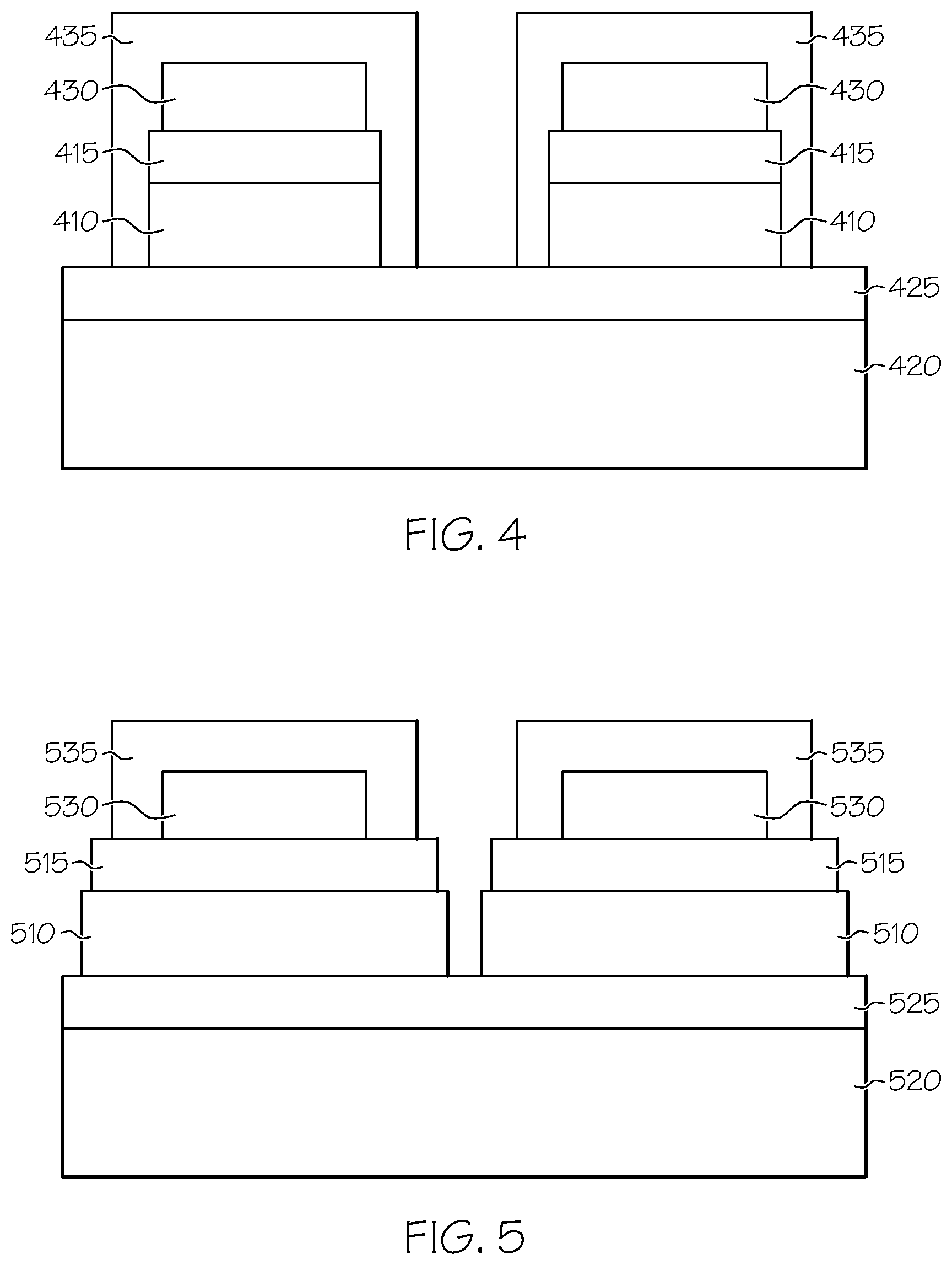
FIG. 4 shows another method of making encapsulated environmentally sensitive devices. The flexible substrate 410 has a pre-applied first barrier stack 415. The individual layers of the barrier stacks are not shown. The flexible substrate 410 is cut into discrete sheets with dimensions appropriate to the environmentally sensitive device 430 to be applied. The discrete sheets of the flexible substrate 410 with the pre-applied first barrier stack 415 are temporarily laminated adjacent to the rigid support 420 with the reversible adhesive 425. The environmentally sensitive device 430 is applied adjacent to the first barrier stack 415, and encapsulated by the second barrier stack 435, which includes an edge seal. The adhesive can be reversed, and the rigid support 420 removed. The individual encapsulated environmentally sensitive devices are separated by the removal of the rigid support 420; separation does not require cutting. This approach allows the creation of an edge seal for the barrier stack edges exposed when the flexible substrate 410 and first barrier stack 415 were cut into discrete sheets.
The adhesive layer 425 can be replaced after each cycle, if desired. This helps to eliminate problems with contaminants and debris becoming trapped in the adhesive.
Another method is shown in FIG. 5. In this arrangement, the flexible support 510 is cut into discrete sheets having an appropriate size for environmentally sensitive device 530. The discrete sheets of the flexible substrate 510 are temporarily laminated to the rigid support 520 with the reversible adhesive 525. The first barrier stack 515, which has an edge seal, is deposited adjacent to the flexible substrate 510. The individual layers of the barrier stacks are not shown. The environmentally sensitive device 530 is fabricated adjacent to the first barrier stack 515, and the second barrier stack 535, which has an edge seal, encapsulates it. The adhesive 525 is reversed, and the rigid support 520 removed. The removal of the rigid support 520 separates the individual encapsulated environmentally sensitive devices; no cutting is necessary.
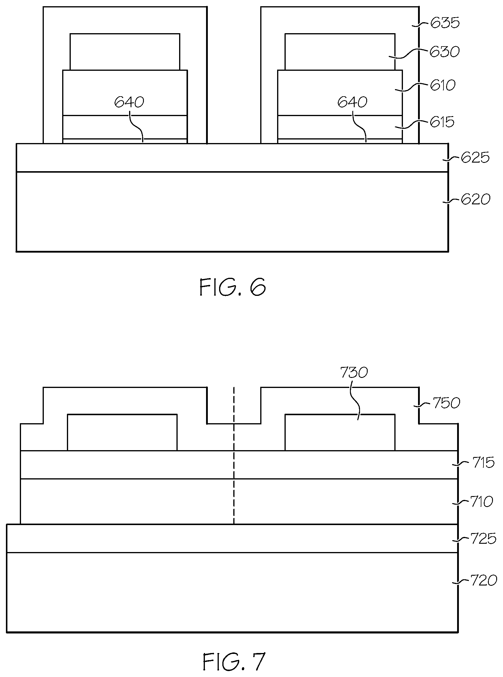
Still another method is shown in FIG. 6. The flexible support 610 has a pre-applied barrier stack 615. The flexible support 610 is cut into discrete sheets sized for the environmentally sensitive device 630. The flexible substrate 610 with the barrier stack 615 is temporarily laminated to the rigid support 620 using a reversible adhesive 625. The individual layers of the barrier stacks are not shown. In this arrangement, the barrier stack 615 faces the adhesive 625, rather than the flexible substrate 610 facing the adhesive 625. An optional functional layer 640, such as a scratch resistant layer, can be included over the barrier stack 615 and would serve as the interface between the barrier stack 615 and the adhesive 625. The environmentally sensitive device 630 is fabricated adjacent to the flexible support 610, and is encapsulated by the second barrier stack 635, which has an edge seal. This arrangement allows the second barrier stack 635 to protect the edges of the first barrier stack 615 which were exposed when the flexible substrate 610 and first barrier stack 615 were cut into discrete sheets.
Alternatively in FIGS. 2-6, the second barrier could be a sheet of a barrier material, such as a sheet of a metal or metal foil, which can be laminated over the environmentally sensitive device. FIG. 7 shows another method of making encapsulated environmentally sensitive devices. In this arrangement, the flexible substrate 710 includes a pre-applied three dimensional barrier 745. The flexible substrate 710 is temporarily laminated to the rigid support 720 using a reversible adhesive 725. The environmentally sensitive device 730 is fabricated adjacent to the flexible support 710. A second three dimensional barrier 750 encapsulates the environmentally sensitive device 730. The adhesive 725 can be reversed, and the rigid support 720 removed. The flexible substrate 710 can be cut to separate the individual encapsulated environmentally sensitive devices. One advantage of the three dimensional first and second barriers is that cutting the barriers does not compromise the barrier. A method of making a three dimensional barrier is described in U.S. application Ser. No. 11/627,583, filed concurrently herewith, entitled "Three Dimensional Multilayer Barrier and Method of Making", which is incorporated by reference herein. Another method is shown in FIG. 8. In this embodiment, there is no barrier stack on the flexible substrate 810. For example, the flexible substrate could be a metal or metal foil. The flexible substrate 810 is temporarily laminated to the rigid support 820 using reversible adhesive 825. A second barrier stack 835 is applied adjacent to the environmentally sensitive device 830. The second barrier stack 835 can be applied by laminating a flexible film 840 with a pre-applied second barrier 835 using an adhesive 845. Other methods of lamination could be used including, but not limited to, using heat. A gettering material could be included between the adhesive 845 and the environmentally sensitive device 830.
A cover sheet could be laminated to an array of environmentally sensitive devices. The adhesive/sealant (and optional getter) could be patterned to surround each of the array of devices on the flexible substrate using a mask or a printing technique such as ink jet. Another method is the use of a layer of adhesive/sealant applied to the entire surface (the devices as well as the area between devices). A third method is to use pick and place equipment to apply individual covers to each of the devices. In this case, the adhesive/sealant could be applied as described in either of the first two approaches.
Alternatively, the second barrier 835 could be deposited adjacent to the environmentally sensitive device 830 using vacuum or atmospheric processes. In this case, the flexible film 840 and adhesive 845 would not be used.
There can be one or more first and/or second barrier stacks. The barrier stacks can include at least one decoupling layer and at least one barrier layer. For example, a suitable arrangement for the encapsulated environmentally sensitive device is shown in FIG. 9. The flexible substrate 910 is temporarily laminated to the rigid support 920 using a reversible adhesive 925. First barrier stacks 915 are adjacent to the flexible substrate 910. The environmentally sensitive device 930 is adjacent to the first barrier stacks 915. The second barrier stacks 935 are adjacent to the environmentally sensitive device 930. The first and second barrier stacks 915, 935 are made of alternating decoupling layers 940 and barrier layers 945. There are five first barrier stacks 915 of alternating decoupling layers and barrier layers, and seven second barrier stacks 935. In the second barrier stacks 935, the barrier layer adjacent to the environmentally sensitive device can be thicker than the other barrier layers, and the last decoupling layer (the top layer) can be thicker than the other decoupling layers, if desired. FIG. 9 shows only the order of the various layers; it does not show the edge seals for the barrier stacks.
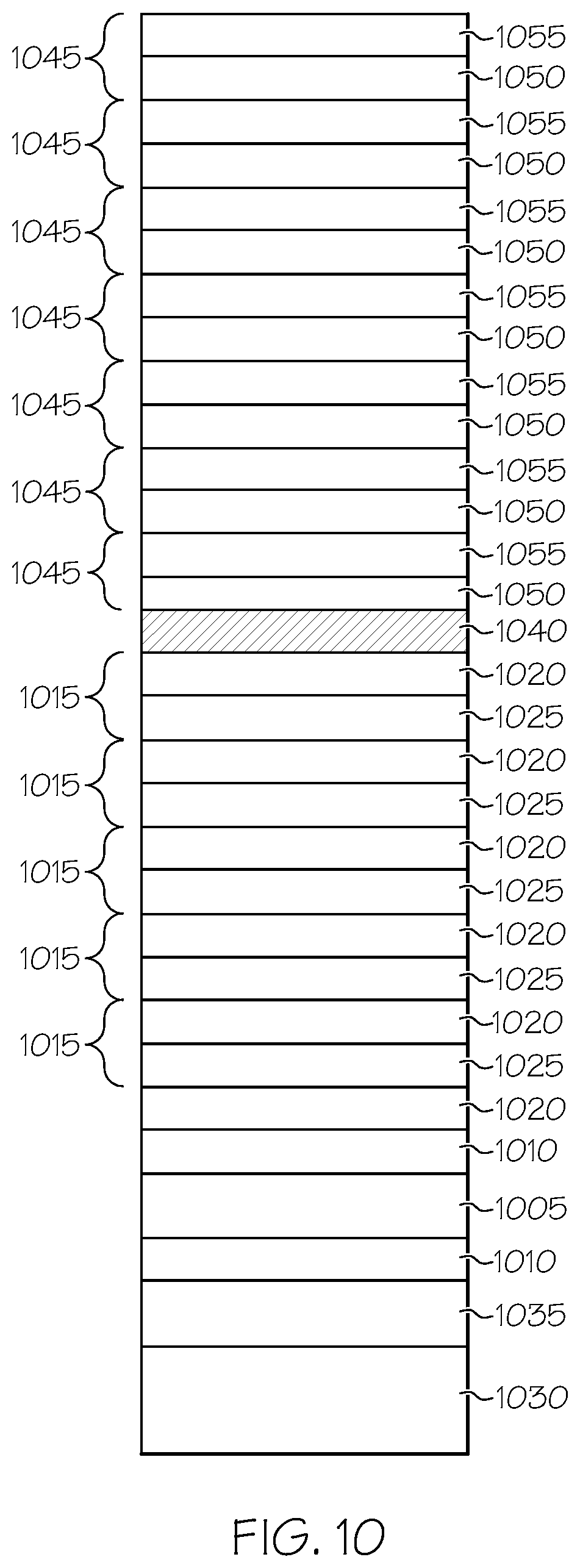
EXAMPLE 1
FIG. 10 shows one embodiment of a structure which was tested. The flexible substrate 1005 was polyethylene naphthenate. It had a hard coat layer (SDC Technology, crystal coat MP 101) 1010 on both sides. It also had pre-applied barrier stacks 1015 containing 5 sets of alternating layers of aluminum oxide 1020 and acrylate polymer 1025 and an additional aluminum oxide layer 1020. The flexible substrate and barrier stacks were temporarily laminated to the rigid glass support 1030 using a reversible adhesive (3M 668 Thermo Bond) 1035. A layer of calcium 1040, which is used to test barrier performance, was then deposited over the first barrier stacks 1015. The calcium test is described in Nisato et al., "Thin Film Encapsulation for OLEDs: Evaluation of Multi-layer Barriers using the Ca Test," SID 03 Digest, 2003, p. 550-553, which is incorporated herein by reference. The second barrier stacks 1045 were then deposited. The second barrier stacks were 7 sets of alternating layers of aluminum oxide 1050 and acrylate polymer 1055. The first oxide layer (adjacent to the layer of calcium 1040) and the last polymer layer (the top layer) were thicker than the remaining layers. These samples had rather short lifetimes, typically about 25 hours at 60.degree. C. and 90% RH. The best results were about 100 hours, but there was significant damage to the barrier coated flexible substrate.
The experiment was repeated by laminating the flexible substrate with the pre-applied barrier stacks to the rigid glass support. Three layers, a fast process aluminum oxide, acrylate polymer, and aluminum oxide were deposited on the barrier stacks prior to deposition and encapsulation of the Ca test patch. This was done to solve issues which were believed to be due to debris from shipping and/or handling of the flexible substrate and barrier stacks. This experiment showed excellent results, with about 90% of the Ca samples passing after 500 hours at 60.degree. C. and 90% RH.
While certain representative embodiments and details have been shown for purposes of illustrating the invention, it will be apparent to those skilled in the art that various changes in the compositions and methods disclosed herein may be made without departing from the scope of the invention, which is defined in the appended claims.
* * * * *
D00000
D00001
D00002
D00003
D00004
D00005
D00006
D00007
XML
uspto.report is an independent third-party trademark research tool that is not affiliated, endorsed, or sponsored by the United States Patent and Trademark Office (USPTO) or any other governmental organization. The information provided by uspto.report is based on publicly available data at the time of writing and is intended for informational purposes only.
While we strive to provide accurate and up-to-date information, we do not guarantee the accuracy, completeness, reliability, or suitability of the information displayed on this site. The use of this site is at your own risk. Any reliance you place on such information is therefore strictly at your own risk.
All official trademark data, including owner information, should be verified by visiting the official USPTO website at www.uspto.gov. This site is not intended to replace professional legal advice and should not be used as a substitute for consulting with a legal professional who is knowledgeable about trademark law.