Wireless power receiver with a synchronous rectifier
Leabman February 16, 2
U.S. patent number 10,923,954 [Application Number 15/803,476] was granted by the patent office on 2021-02-16 for wireless power receiver with a synchronous rectifier. This patent grant is currently assigned to Energous Corporation. The grantee listed for this patent is Energous Corporation. Invention is credited to Michael A. Leabman.
| United States Patent | 10,923,954 |
| Leabman | February 16, 2021 |
Wireless power receiver with a synchronous rectifier
Abstract
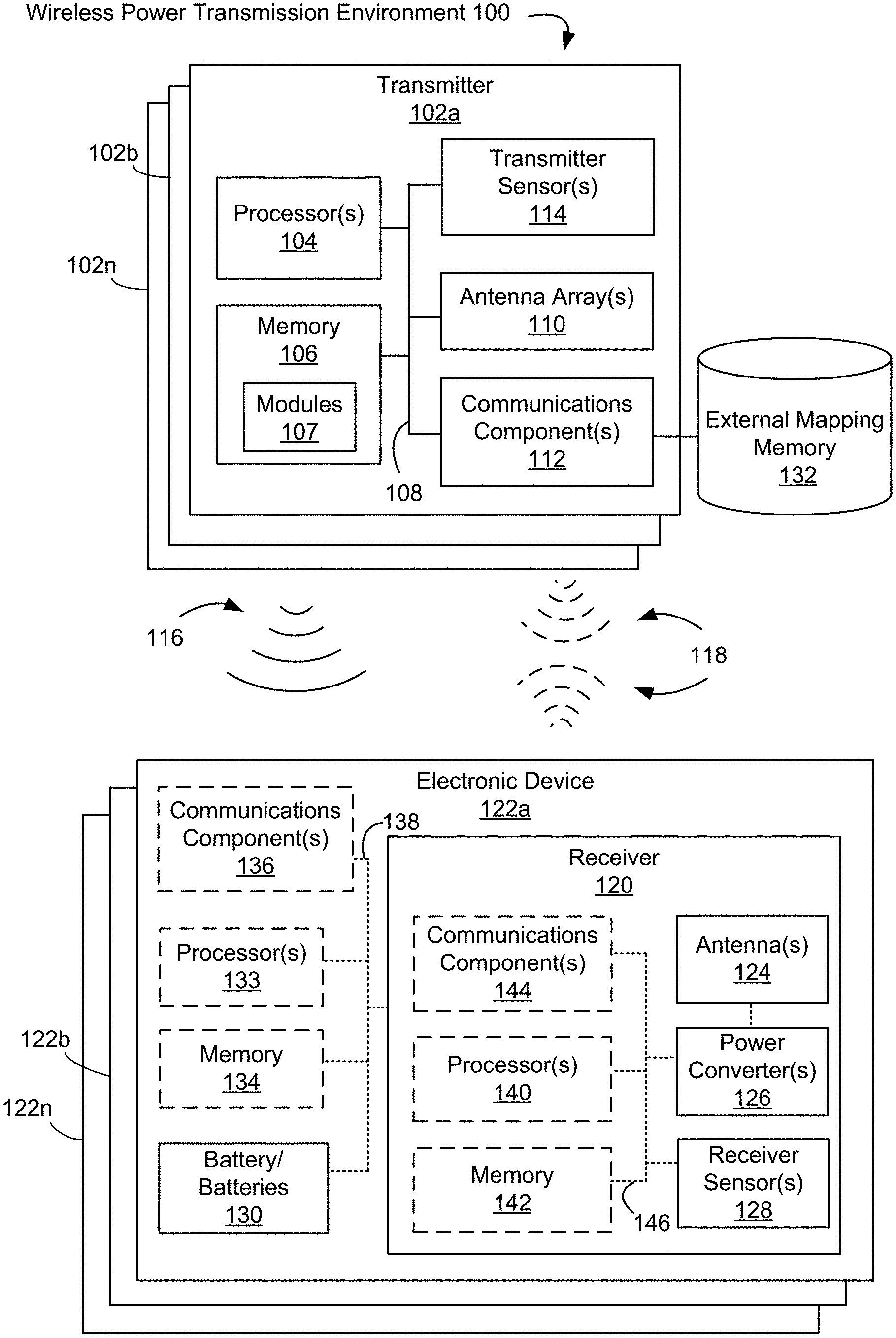
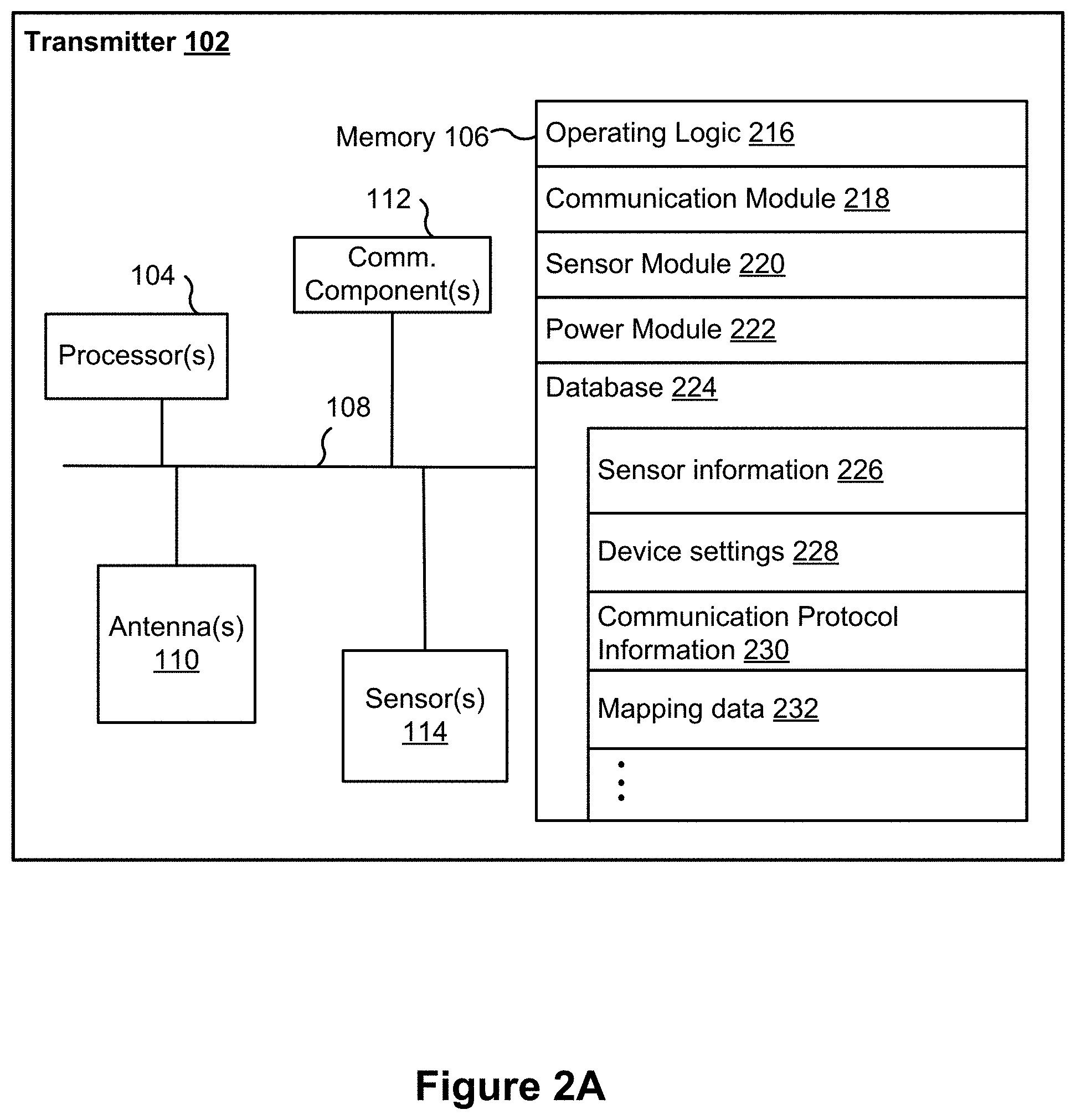
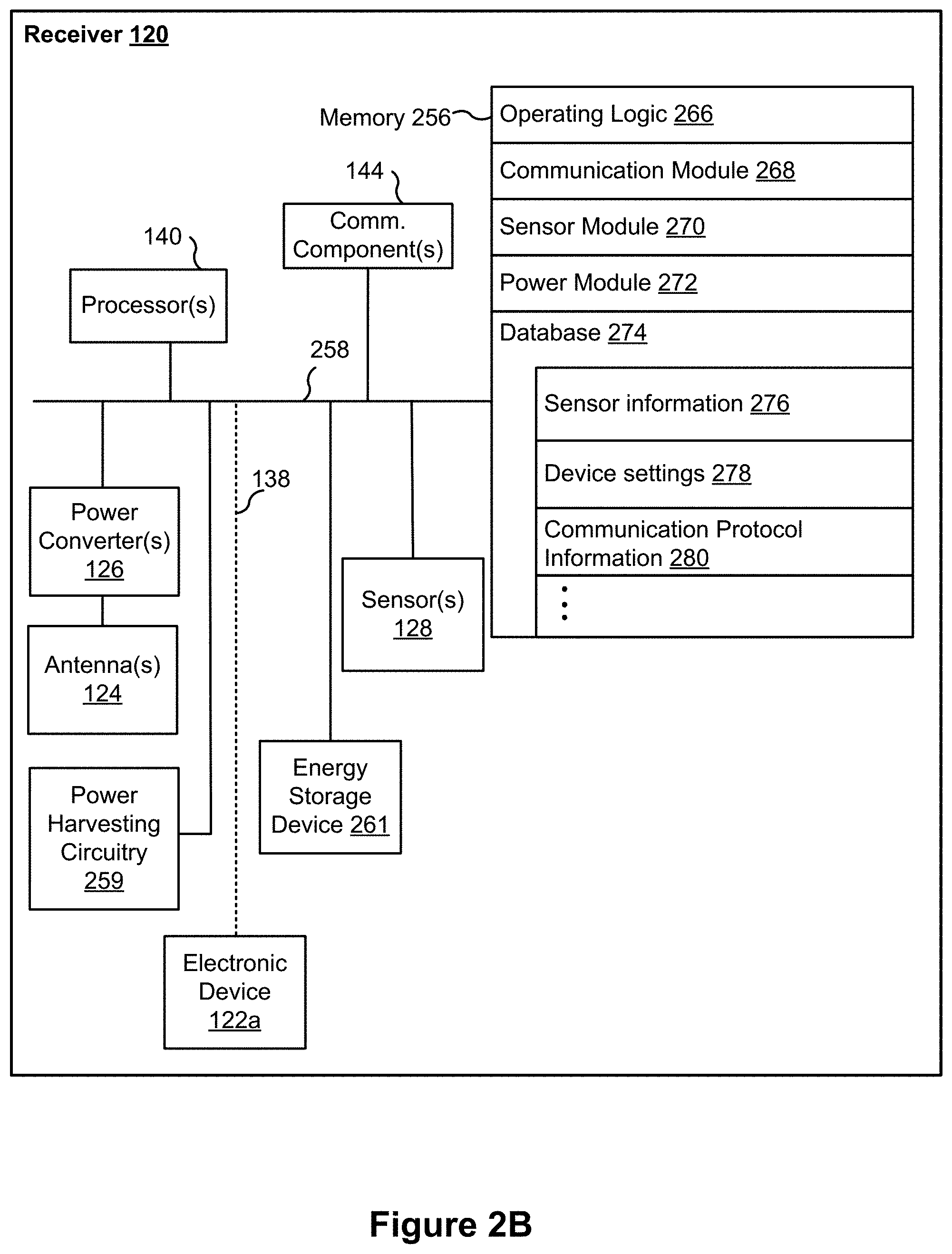
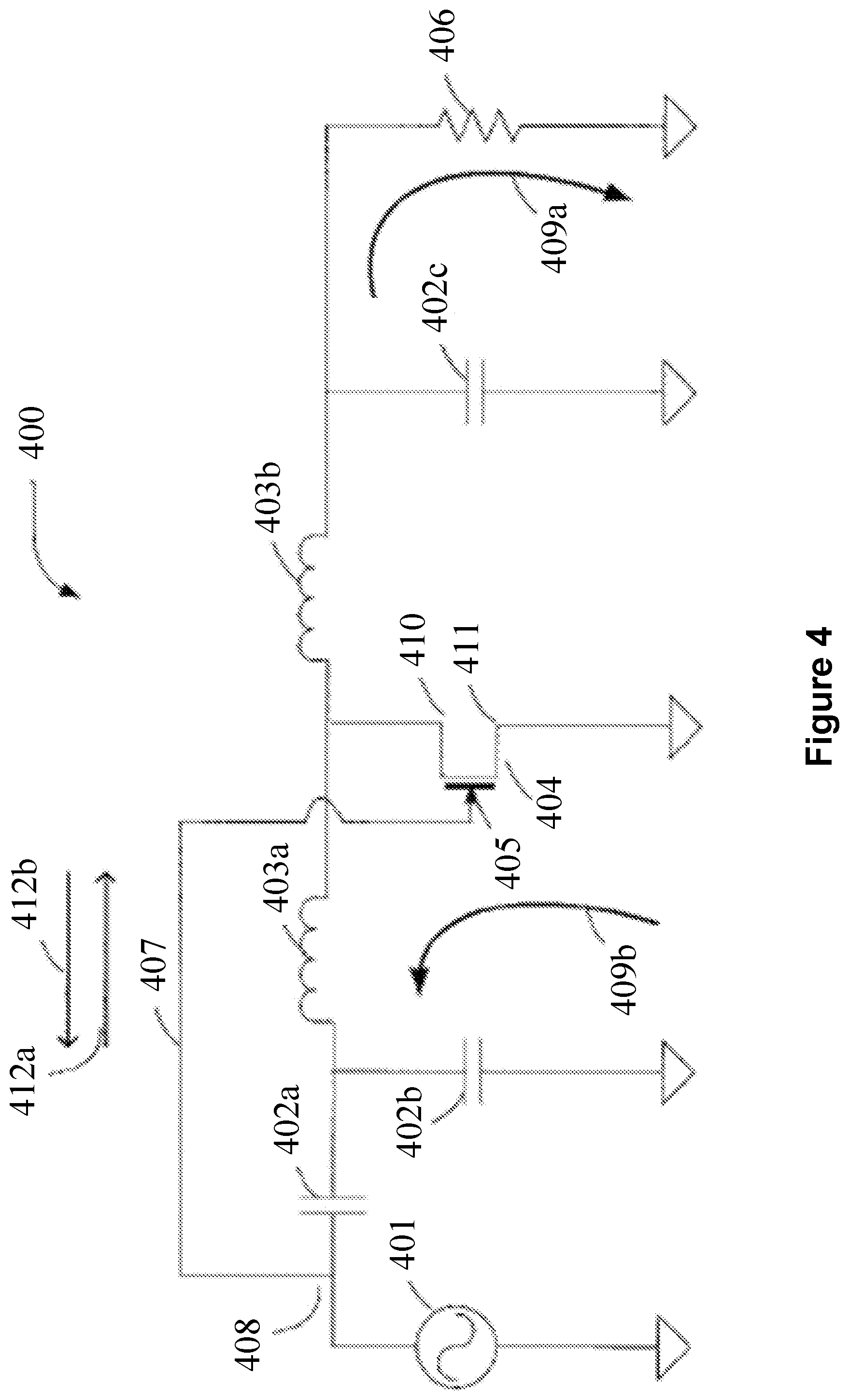
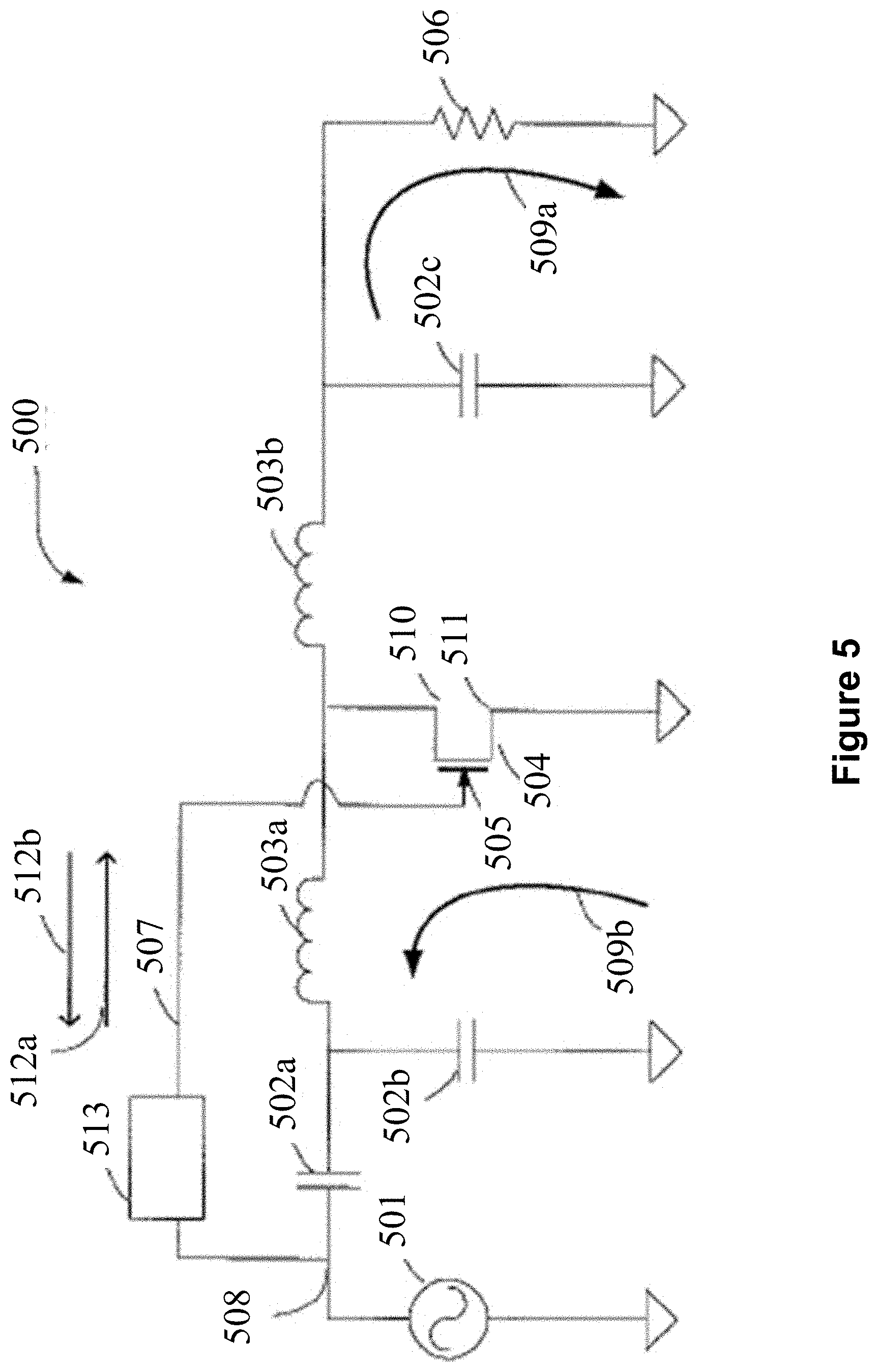
Embodiments disclosed herein describe a wireless power receiver including a synchronous rectifier using a Class-E or a Class-F amplifier. The voltage waveform generated from a power source, for example an antenna, is tapped to create a feed-forward tap-line to provide a gate voltage to the transistor of the Class-E or the Class-F amplifier. In some instances, a constant phase shift across the feed-forward tap-line may be provided using a micro-strip of a predetermined length that is selected such that the transistor switches at the zero-crossings of the voltage waveform arriving at the drain terminal of the transmitter. In other instances, a feed-forward circuit is used for controlling the phase across the feed-forward loop.
| Inventors: | Leabman; Michael A. (Pleasanton, CA) | ||||||||||
|---|---|---|---|---|---|---|---|---|---|---|---|
| Applicant: |
|
||||||||||
| Assignee: | Energous Corporation (San Jose,
CA) |
||||||||||
| Family ID: | 1000005369236 | ||||||||||
| Appl. No.: | 15/803,476 | ||||||||||
| Filed: | November 3, 2017 |
Prior Publication Data
| Document Identifier | Publication Date | |
|---|---|---|
| US 20180123400 A1 | May 3, 2018 | |
Related U.S. Patent Documents
| Application Number | Filing Date | Patent Number | Issue Date | ||
|---|---|---|---|---|---|
| 62417115 | Nov 3, 2016 | ||||
| Current U.S. Class: | 1/1 |
| Current CPC Class: | H02J 50/20 (20160201); H02M 3/33592 (20130101); H02J 50/12 (20160201); H03F 3/193 (20130101); H03F 3/2176 (20130101); H03F 1/3223 (20130101); H02M 7/217 (20130101); Y02B 70/10 (20130101) |
| Current International Class: | H02J 7/00 (20060101); H02J 50/12 (20160101); H02K 7/14 (20060101); H03F 1/32 (20060101); H03F 3/217 (20060101); H02J 7/02 (20160101); H03F 3/193 (20060101); H02J 50/20 (20160101); H02M 3/335 (20060101); H02M 7/217 (20060101) |
| Field of Search: | ;320/108 |
References Cited [Referenced By]
U.S. Patent Documents
| 787412 | April 1905 | Tesla |
| 2811624 | October 1957 | Haagensen |
| 2863148 | December 1958 | Gammon et al. |
| 3167775 | January 1965 | Guertler |
| 3434678 | March 1969 | Brown et al. |
| 3696384 | October 1972 | Lester |
| 3754269 | August 1973 | Clavin |
| 4101895 | July 1978 | Jones, Jr. |
| 4360741 | November 1982 | Fitzsimmons et al. |
| 4944036 | July 1990 | Hyatt |
| 4995010 | February 1991 | Knight |
| 5200759 | April 1993 | McGinnis |
| 5211471 | May 1993 | Rohrs |
| 5276455 | January 1994 | Fitzsimmons et al. |
| 5548292 | August 1996 | Hirshfield et al. |
| 5556749 | September 1996 | Mitsuhashi et al. |
| 5568088 | October 1996 | Dent et al. |
| 5631572 | May 1997 | Sheen et al. |
| 5646633 | July 1997 | Dahlberg |
| 5697063 | December 1997 | Kishigami et al. |
| 5712642 | January 1998 | Hulderman |
| 5936527 | August 1999 | Isaacman et al. |
| 5982139 | November 1999 | Parise |
| 6046708 | April 2000 | MacDonald, Jr. et al. |
| 6061025 | May 2000 | Jackson et al. |
| 6127799 | October 2000 | Krishnan |
| 6127942 | October 2000 | Welle |
| 6163296 | December 2000 | Lier et al. |
| 6176433 | January 2001 | Uesaka et al. |
| 6271799 | August 2001 | Rief |
| 6289237 | September 2001 | Mickle et al. |
| 6329908 | December 2001 | Frecska |
| 6400586 | June 2002 | Raddi et al. |
| 6421235 | July 2002 | Ditzik |
| 6437685 | August 2002 | Hanaki |
| 6456253 | September 2002 | Rummeli et al. |
| 6476795 | November 2002 | Derocher et al. |
| 6501414 | December 2002 | Amdt et al. |
| 6583723 | June 2003 | Watanabe et al. |
| 6597897 | July 2003 | Tang |
| 6615074 | September 2003 | Mickle et al. |
| 6650376 | November 2003 | Obitsu |
| 6664920 | December 2003 | Mott et al. |
| 6680700 | January 2004 | Hilgers |
| 6798716 | September 2004 | Charych |
| 6803744 | October 2004 | Sabo |
| 6853197 | February 2005 | McFarland |
| 6856291 | February 2005 | Mickle et al. |
| 6911945 | June 2005 | Korva |
| 6960968 | November 2005 | Odendaal et al. |
| 6967462 | November 2005 | Landis |
| 6988026 | January 2006 | Breed et al. |
| 7003350 | February 2006 | Denker et al. |
| 7012572 | March 2006 | Schaffner et al. |
| 7027311 | April 2006 | Vanderelli et al. |
| 7068234 | June 2006 | Sievenpiper |
| 7068991 | June 2006 | Parise |
| 7079079 | July 2006 | Jo et al. |
| 7183748 | February 2007 | Unno et al. |
| 7191013 | March 2007 | Miranda et al. |
| 7193644 | March 2007 | Carter |
| 7196663 | March 2007 | Bolzer et al. |
| 7205749 | April 2007 | Hagen et al. |
| 7215296 | May 2007 | Abramov et al. |
| 7222356 | May 2007 | Yonezawa et al. |
| 7274334 | September 2007 | o'Riordan et al. |
| 7274336 | September 2007 | Carson |
| 7351975 | April 2008 | Brady et al. |
| 7359730 | April 2008 | Dennis et al. |
| 7372408 | May 2008 | Gaucher |
| 7392068 | June 2008 | Dayan |
| 7403803 | July 2008 | Mickle et al. |
| 7443057 | October 2008 | Nunally |
| 7451839 | November 2008 | Perlman |
| 7463201 | December 2008 | Chiang et al. |
| 7471247 | December 2008 | Saily |
| 7535195 | May 2009 | Horovitz et al. |
| 7614556 | November 2009 | Overhultz et al. |
| 7639994 | December 2009 | Greene et al. |
| 7643312 | January 2010 | Vanderelli et al. |
| 7652577 | January 2010 | Madhow et al. |
| 7679576 | March 2010 | Riedel et al. |
| 7702771 | April 2010 | Ewing et al. |
| 7786419 | August 2010 | Hyde et al. |
| 7812771 | October 2010 | Greene et al. |
| 7830312 | November 2010 | Choudhury et al. |
| 7844306 | November 2010 | Shearer et al. |
| 7868482 | January 2011 | Greene et al. |
| 7898105 | March 2011 | Greene et al. |
| 7904117 | March 2011 | Doan et al. |
| 7911386 | March 2011 | Itoh et al. |
| 7925308 | April 2011 | Greene et al. |
| 7948208 | May 2011 | Partovi et al. |
| 8049676 | November 2011 | Yoon et al. |
| 8055003 | November 2011 | Mittleman et al. |
| 8070595 | December 2011 | Alderucci et al. |
| 8072380 | December 2011 | Crouch |
| 8092301 | January 2012 | Alderucci et al. |
| 8099140 | January 2012 | Arai |
| 8115448 | February 2012 | John |
| 8159090 | April 2012 | Greene et al. |
| 8159364 | April 2012 | Zeine |
| 8180286 | May 2012 | Yamasuge |
| 8184454 | May 2012 | Mao |
| 8228194 | July 2012 | Mickle |
| 8234509 | July 2012 | Gioscia et al. |
| 8264101 | September 2012 | Hyde et al. |
| 8264291 | September 2012 | Morita |
| 8276325 | October 2012 | Clifton et al. |
| 8278784 | October 2012 | Cook et al. |
| 8284101 | October 2012 | Fusco |
| 8310201 | November 2012 | Wright |
| 8338991 | December 2012 | Von Novak et al. |
| 8362745 | January 2013 | Tinaphong |
| 8380255 | February 2013 | Shearer et al. |
| 8384600 | February 2013 | Huang et al. |
| 8410953 | April 2013 | Zeine |
| 8411963 | April 2013 | Luff |
| 8432062 | April 2013 | Greene et al. |
| 8432071 | April 2013 | Huang et al. |
| 8446248 | May 2013 | Zeine |
| 8447234 | May 2013 | Cook et al. |
| 8451189 | May 2013 | Fluhler |
| 8452235 | May 2013 | Kirby et al. |
| 8457656 | June 2013 | Perkins et al. |
| 8461817 | June 2013 | Martin et al. |
| 8467733 | June 2013 | Leabman |
| 8497601 | July 2013 | Hall et al. |
| 8497658 | July 2013 | Von Novak et al. |
| 8552597 | August 2013 | Song et al. |
| 8558661 | October 2013 | Zeine |
| 8560026 | October 2013 | Chanterac |
| 8564485 | October 2013 | Milosavljevic et al. |
| 8604746 | December 2013 | Lee |
| 8614643 | December 2013 | Leabman |
| 8621245 | December 2013 | Shearer et al. |
| 8626249 | January 2014 | Kuusilinna et al. |
| 8629576 | January 2014 | Levine |
| 8653966 | February 2014 | Rao et al. |
| 8674551 | March 2014 | Low et al. |
| 8686685 | April 2014 | Moshfeghi |
| 8686905 | April 2014 | Shtrom |
| 8712355 | April 2014 | Black et al. |
| 8712485 | April 2014 | Tam |
| 8718773 | May 2014 | Wills et al. |
| 8729737 | May 2014 | Schatz et al. |
| 8736228 | May 2014 | Freed et al. |
| 8760113 | June 2014 | Keating |
| 8770482 | July 2014 | Ackermann et al. |
| 8772960 | July 2014 | Yoshida |
| 8823319 | September 2014 | Von Novak, III et al. |
| 8832646 | September 2014 | Wendling |
| 8854176 | October 2014 | Zeine |
| 8860364 | October 2014 | Low et al. |
| 8897770 | November 2014 | Frolov et al. |
| 8903456 | December 2014 | Chu et al. |
| 8917057 | December 2014 | Hui |
| 8923189 | December 2014 | Leabman |
| 8928544 | January 2015 | Massie et al. |
| 8937408 | January 2015 | Ganem et al. |
| 8946940 | February 2015 | Kim et al. |
| 8963486 | February 2015 | Kirby et al. |
| 8970070 | March 2015 | Sada et al. |
| 8989053 | March 2015 | Skaaksrud et al. |
| 9000616 | April 2015 | Greene et al. |
| 9001622 | April 2015 | Perry |
| 9006934 | April 2015 | Kozakai et al. |
| 9021277 | April 2015 | Shearer et al. |
| 9030161 | May 2015 | Lu et al. |
| 9059598 | June 2015 | Kang et al. |
| 9059599 | June 2015 | Won et al. |
| 9077188 | July 2015 | Moshfeghi |
| 9083595 | July 2015 | Rakib et al. |
| 9088216 | July 2015 | Garrity et al. |
| 9124125 | September 2015 | Leabman et al. |
| 9130397 | September 2015 | Leabman et al. |
| 9130602 | September 2015 | Cook |
| 9142998 | September 2015 | Yu et al. |
| 9143000 | September 2015 | Leabman et al. |
| 9143010 | September 2015 | Urano |
| 9153074 | October 2015 | Zhou et al. |
| 9178389 | November 2015 | Hwang |
| 9225196 | December 2015 | Huang et al. |
| 9240469 | January 2016 | Sun et al. |
| 9242411 | January 2016 | Kritchman et al. |
| 9244500 | January 2016 | Cain et al. |
| 9252628 | February 2016 | Leabman et al. |
| 9270344 | February 2016 | Rosenberg |
| 9276329 | March 2016 | Jones et al. |
| 9282582 | March 2016 | Dunsbergen et al. |
| 9294840 | March 2016 | Anderson et al. |
| 9297896 | March 2016 | Andrews |
| 9318898 | April 2016 | John |
| 9368020 | June 2016 | Bell et al. |
| 9401977 | July 2016 | Gaw |
| 9409490 | August 2016 | Kawashima |
| 9419335 | August 2016 | Pintos |
| 9438045 | September 2016 | Leabman |
| 9438046 | September 2016 | Leabman |
| 9444283 | September 2016 | Son et al. |
| 9450449 | September 2016 | Leabman et al. |
| 9461502 | October 2016 | Lee et al. |
| 9520725 | December 2016 | Masaoka et al. |
| 9520748 | December 2016 | Hyde et al. |
| 9522270 | December 2016 | Perryman et al. |
| 9532748 | January 2017 | Denison et al. |
| 9537354 | January 2017 | Bell et al. |
| 9537357 | January 2017 | Leabman |
| 9537358 | January 2017 | Leabman |
| 9538382 | January 2017 | Bell et al. |
| 9544640 | January 2017 | Lau |
| 9559553 | January 2017 | Bae |
| 9564773 | February 2017 | Pogorelik et al. |
| 9571974 | February 2017 | Choi et al. |
| 9590317 | March 2017 | Zimmerman et al. |
| 9590444 | March 2017 | Walley |
| 9620996 | April 2017 | Zeine |
| 9647328 | May 2017 | Dobric |
| 9706137 | July 2017 | Scanlon et al. |
| 9711999 | July 2017 | Hietala et al. |
| 9723635 | August 2017 | Nambord et al. |
| 9793758 | October 2017 | Leabman |
| 9793764 | October 2017 | Perry |
| 9800172 | October 2017 | Leabman |
| 9806564 | October 2017 | Leabman |
| 9819230 | November 2017 | Petras et al. |
| 9825674 | November 2017 | Leabman |
| 9843229 | December 2017 | Leabman |
| 9847669 | December 2017 | Leabman |
| 9847677 | December 2017 | Leabman |
| 9853361 | December 2017 | Chen et al. |
| 9853692 | December 2017 | Bell et al. |
| 9859758 | January 2018 | Leabman |
| 9866279 | January 2018 | Bell et al. |
| 9867032 | January 2018 | Verma et al. |
| 9871301 | January 2018 | Contopanagos |
| 9876380 | January 2018 | Leabman et al. |
| 9876394 | January 2018 | Leabman |
| 9876536 | January 2018 | Bell et al. |
| 9882394 | January 2018 | Bell et al. |
| 9887584 | February 2018 | Bell et al. |
| 9893555 | February 2018 | Leabman et al. |
| 9893564 | February 2018 | de Rochemont |
| 9899744 | February 2018 | Contopanagos et al. |
| 9899844 | February 2018 | Bell et al. |
| 9899861 | February 2018 | Leabman et al. |
| 9916485 | March 2018 | Lilly et al. |
| 9917477 | March 2018 | Bell et al. |
| 9923386 | March 2018 | Leabman et al. |
| 9939864 | April 2018 | Bell et al. |
| 9965009 | May 2018 | Bell et al. |
| 9966765 | May 2018 | Leabman |
| 9966784 | May 2018 | Leabman |
| 9967743 | May 2018 | Bell et al. |
| 9973008 | May 2018 | Leabman |
| 10003211 | June 2018 | Leabman et al. |
| 10008777 | June 2018 | Broyde et al. |
| 10014728 | July 2018 | Leabman |
| 10027159 | July 2018 | Hosseini |
| 10038337 | July 2018 | Leabman et al. |
| 10050462 | August 2018 | Leabman et al. |
| 10056782 | August 2018 | Leabman |
| 10063064 | August 2018 | Bell et al. |
| 10068703 | September 2018 | Contopanagos |
| 10075008 | September 2018 | Bell et al. |
| 10090699 | October 2018 | Leabman |
| 10090714 | October 2018 | Bohn et al. |
| 10090886 | October 2018 | Bell et al. |
| 10103552 | October 2018 | Leabman et al. |
| 10110046 | October 2018 | Esquibel et al. |
| 10122219 | November 2018 | Hosseini et al. |
| 10124754 | November 2018 | Leabman |
| 10128686 | November 2018 | Leabman et al. |
| 10134260 | November 2018 | Bell et al. |
| 10135112 | November 2018 | Hosseini |
| 10135294 | November 2018 | Leabman |
| 10141771 | November 2018 | Hosseini et al. |
| 10148097 | December 2018 | Leabman et al. |
| 10153645 | December 2018 | Bell et al. |
| 10153653 | December 2018 | Bell et al. |
| 10153660 | December 2018 | Leabman et al. |
| 10158257 | December 2018 | Leabman |
| 10158259 | December 2018 | Leabman |
| 10164478 | December 2018 | Leabman |
| 10170917 | January 2019 | Bell et al. |
| 10181756 | January 2019 | Bae et al. |
| 10186892 | January 2019 | Hosseini et al. |
| 10193396 | January 2019 | Bell et al. |
| 10199835 | February 2019 | Bell |
| 10199849 | February 2019 | Bell |
| 10205239 | February 2019 | Contopanagos et al. |
| 10211674 | February 2019 | Leabman et al. |
| 10223717 | March 2019 | Bell |
| 10224758 | March 2019 | Leabman et al. |
| 10224982 | March 2019 | Leabman |
| 10230266 | March 2019 | Leabman et al. |
| 10243414 | March 2019 | Leabman et al. |
| 10256657 | April 2019 | Hosseini et al. |
| 10256677 | April 2019 | Hosseini et al. |
| 10263432 | April 2019 | Leabman et al. |
| 10291055 | May 2019 | Bell et al. |
| 10291066 | May 2019 | Leabman |
| 10291294 | May 2019 | Leabman |
| 10298024 | May 2019 | Leabman |
| 10298133 | May 2019 | Leabman |
| 10305315 | May 2019 | Leabman et al. |
| 10312715 | June 2019 | Leabman |
| 10333332 | June 2019 | Hosseini |
| 10396588 | August 2019 | Leabman |
| 10490346 | November 2019 | Contopanagos |
| 10491029 | November 2019 | Hosseini |
| 10498144 | December 2019 | Leabman et al. |
| 10511097 | December 2019 | Kornaros et al. |
| 10516301 | December 2019 | Leabman |
| 10523058 | December 2019 | Leabman |
| 10615647 | April 2020 | Johnston et al. |
| 10714984 | July 2020 | Hosseini et al. |
| 2001/0027876 | October 2001 | Tsukamoto et al. |
| 2002/0001307 | January 2002 | Nguyen et al. |
| 2002/0024471 | February 2002 | Ishitobi |
| 2002/0028655 | March 2002 | Rosener et al. |
| 2002/0034958 | March 2002 | Oberschmidt et al. |
| 2002/0054330 | May 2002 | Jinbo et al. |
| 2002/0065052 | May 2002 | Pande et al. |
| 2002/0072784 | June 2002 | Sheppard et al. |
| 2002/0095980 | July 2002 | Breed et al. |
| 2002/0103447 | August 2002 | Terry |
| 2002/0123776 | September 2002 | Von Arx |
| 2002/0133592 | September 2002 | Matsuda |
| 2002/0171594 | November 2002 | Fang |
| 2002/0172223 | November 2002 | Stilp |
| 2003/0005759 | January 2003 | Breed et al. |
| 2003/0038750 | February 2003 | Chen |
| 2003/0058187 | March 2003 | Billiet et al. |
| 2003/0076274 | April 2003 | Phelan et al. |
| 2003/0179152 | September 2003 | Watada et al. |
| 2003/0179573 | September 2003 | Chun |
| 2003/0192053 | October 2003 | Sheppard et al. |
| 2004/0019624 | January 2004 | Sukegawa |
| 2004/0020100 | February 2004 | O'Brien et al. |
| 2004/0036657 | February 2004 | Forster et al. |
| 2004/0066251 | April 2004 | Eleftheriades et al. |
| 2004/0107641 | June 2004 | Walton et al. |
| 2004/0113543 | June 2004 | Daniels |
| 2004/0119675 | June 2004 | Washio et al. |
| 2004/0130425 | July 2004 | Dayan et al. |
| 2004/0130442 | July 2004 | Breed |
| 2004/0142733 | July 2004 | Parise |
| 2004/0145342 | July 2004 | Lyon |
| 2004/0155832 | August 2004 | Yuanzhu |
| 2004/0196190 | October 2004 | Mendolia et al. |
| 2004/0203979 | October 2004 | Attar et al. |
| 2004/0207559 | October 2004 | Milosavljevic |
| 2004/0218759 | November 2004 | Yacobi |
| 2004/0241402 | December 2004 | Kawate |
| 2004/0259604 | December 2004 | Mickle et al. |
| 2004/0263124 | December 2004 | Wieck et al. |
| 2005/0007276 | January 2005 | Barrick et al. |
| 2005/0030118 | February 2005 | Wang |
| 2005/0046584 | March 2005 | Breed |
| 2005/0055316 | March 2005 | Williams |
| 2005/0077872 | April 2005 | Single |
| 2005/0093766 | May 2005 | Turner |
| 2005/0116683 | June 2005 | Cheng |
| 2005/0117660 | June 2005 | Vialle et al. |
| 2005/0134517 | June 2005 | Gottl |
| 2005/0171411 | August 2005 | KenKnight et al. |
| 2005/0198673 | September 2005 | Kit et al. |
| 2005/0227619 | October 2005 | Lee et al. |
| 2005/0232469 | October 2005 | Schofield |
| 2005/0237249 | October 2005 | Nage l |
| 2005/0237258 | October 2005 | Abramov et al. |
| 2005/0282591 | December 2005 | Shaff |
| 2006/0013335 | January 2006 | Leabman |
| 2006/0019712 | January 2006 | Choi |
| 2006/0030279 | February 2006 | Leabman et al. |
| 2006/0033674 | February 2006 | Essig, Jr. et al. |
| 2006/0056855 | March 2006 | Nakagawa et al. |
| 2006/0071308 | April 2006 | Tang et al. |
| 2006/0092079 | May 2006 | de Rochemont |
| 2006/0094425 | May 2006 | Mickle et al. |
| 2006/0113955 | June 2006 | Nunally |
| 2006/0119532 | June 2006 | Yun et al. |
| 2006/0136004 | June 2006 | Cowan et al. |
| 2006/0160517 | July 2006 | Yoon |
| 2006/0183473 | August 2006 | Ukon |
| 2006/0190063 | August 2006 | Kanzius |
| 2006/0192913 | August 2006 | Shutou et al. |
| 2006/0199620 | September 2006 | Greene et al. |
| 2006/0238365 | October 2006 | Vecchione et al. |
| 2006/0266564 | November 2006 | Perlman et al. |
| 2006/0266917 | November 2006 | Baldis et al. |
| 2006/0278706 | December 2006 | Hatakayama et al. |
| 2006/0284593 | December 2006 | Nagy et al. |
| 2006/0287094 | December 2006 | Mahaffey et al. |
| 2007/0007821 | January 2007 | Rossetti |
| 2007/0019693 | January 2007 | Graham |
| 2007/0021140 | January 2007 | Keyes |
| 2007/0060185 | March 2007 | Simon et al. |
| 2007/0070490 | March 2007 | Tsunoda et al. |
| 2007/0090997 | April 2007 | Brown et al. |
| 2007/0093269 | April 2007 | Leabman et al. |
| 2007/0097653 | May 2007 | Gilliland et al. |
| 2007/0103110 | May 2007 | Sagoo |
| 2007/0106894 | May 2007 | Zhang |
| 2007/0109121 | May 2007 | Cohen |
| 2007/0139000 | June 2007 | Kozuma |
| 2007/0149162 | June 2007 | Greene et al. |
| 2007/0164868 | July 2007 | Deavours et al. |
| 2007/0173196 | July 2007 | Gallic |
| 2007/0173214 | July 2007 | Mickle et al. |
| 2007/0178857 | August 2007 | Greene et al. |
| 2007/0178945 | August 2007 | Cook et al. |
| 2007/0182367 | August 2007 | Partovi |
| 2007/0191074 | August 2007 | Harrist et al. |
| 2007/0191075 | August 2007 | Greene et al. |
| 2007/0197281 | August 2007 | Stronach |
| 2007/0210960 | September 2007 | Rofougaran et al. |
| 2007/0222681 | September 2007 | Greene et al. |
| 2007/0228833 | October 2007 | Stevens et al. |
| 2007/0229261 | October 2007 | Zimmerman et al. |
| 2007/0240297 | October 2007 | Yang et al. |
| 2007/0257634 | November 2007 | Leschin et al. |
| 2007/0273486 | November 2007 | Shiotsu |
| 2007/0291165 | December 2007 | Wang |
| 2007/0296639 | December 2007 | Hook et al. |
| 2007/0298846 | December 2007 | Greene et al. |
| 2008/0014897 | January 2008 | Cook et al. |
| 2008/0024376 | January 2008 | Norris et al. |
| 2008/0048917 | February 2008 | Achour et al. |
| 2008/0062062 | March 2008 | Borau et al. |
| 2008/0062255 | March 2008 | Gal |
| 2008/0067874 | March 2008 | Tseng |
| 2008/0074324 | March 2008 | Puzella et al. |
| 2008/0089277 | April 2008 | Aledander et al. |
| 2008/0110263 | May 2008 | Klessel et al. |
| 2008/0113816 | May 2008 | Mahaffey et al. |
| 2008/0122297 | May 2008 | Arai |
| 2008/0123383 | May 2008 | Shionoiri |
| 2008/0129536 | June 2008 | Randall et al. |
| 2008/0140278 | June 2008 | Breed |
| 2008/0169910 | July 2008 | Greene et al. |
| 2008/0197802 | August 2008 | Onishi |
| 2008/0204342 | August 2008 | Kharadly |
| 2008/0204350 | August 2008 | Tam et al. |
| 2008/0210762 | September 2008 | Osada et al. |
| 2008/0211458 | September 2008 | Lawther et al. |
| 2008/0233890 | September 2008 | Baker |
| 2008/0248758 | October 2008 | Schedelbeck et al. |
| 2008/0248846 | October 2008 | Stronach et al. |
| 2008/0258993 | October 2008 | Gummalla et al. |
| 2008/0266191 | October 2008 | Hilgers |
| 2008/0278378 | November 2008 | Chang et al. |
| 2008/0309452 | December 2008 | Zeine |
| 2009/0002493 | January 2009 | Kates |
| 2009/0010316 | January 2009 | Rofougaran et al. |
| 2009/0019183 | January 2009 | Wu et al. |
| 2009/0036065 | February 2009 | Siu |
| 2009/0039828 | February 2009 | Jakubowski |
| 2009/0047998 | February 2009 | Alberth, Jr. |
| 2009/0058354 | March 2009 | Harrison |
| 2009/0058361 | March 2009 | John |
| 2009/0058731 | March 2009 | Geary et al. |
| 2009/0060012 | March 2009 | Gresset et al. |
| 2009/0067198 | March 2009 | Graham et al. |
| 2009/0067208 | March 2009 | Martin et al. |
| 2009/0073066 | March 2009 | Jordon et al. |
| 2009/0096412 | April 2009 | Huang |
| 2009/0096413 | April 2009 | Partovi |
| 2009/0102292 | April 2009 | Cook et al. |
| 2009/0102296 | April 2009 | Greene et al. |
| 2009/0108679 | April 2009 | Porwal |
| 2009/0122847 | May 2009 | Nysen et al. |
| 2009/0128262 | May 2009 | Lee et al. |
| 2009/0157911 | June 2009 | Aihara |
| 2009/0174604 | July 2009 | Keskitalo |
| 2009/0180653 | July 2009 | Sjursen et al. |
| 2009/0200985 | August 2009 | Zane et al. |
| 2009/0206791 | August 2009 | Jung |
| 2009/0207090 | August 2009 | Pettus et al. |
| 2009/0207092 | August 2009 | Nysen et al. |
| 2009/0218884 | September 2009 | Soar |
| 2009/0218891 | September 2009 | McCollough |
| 2009/0219903 | September 2009 | Alamouti et al. |
| 2009/0243397 | October 2009 | Cook et al. |
| 2009/0256752 | October 2009 | Akkermans et al. |
| 2009/0264069 | October 2009 | Yamasuge |
| 2009/0271048 | October 2009 | Wakamatsu |
| 2009/0280866 | November 2009 | Lo et al. |
| 2009/0281678 | November 2009 | Wakamatsu |
| 2009/0284082 | November 2009 | Mohammadian |
| 2009/0284083 | November 2009 | Karalis et al. |
| 2009/0284220 | November 2009 | Toncich et al. |
| 2009/0284227 | November 2009 | Mohammadian et al. |
| 2009/0284325 | November 2009 | Rossiter et al. |
| 2009/0286475 | November 2009 | Toncich et al. |
| 2009/0286476 | November 2009 | Toncich et al. |
| 2009/0291634 | November 2009 | Saarisalo |
| 2009/0299175 | December 2009 | Bernstein et al. |
| 2009/0308936 | December 2009 | Nitzan et al. |
| 2009/0312046 | December 2009 | Clevenger et al. |
| 2009/0315412 | December 2009 | Yamamoto et al. |
| 2009/0322281 | December 2009 | Kamijo et al. |
| 2010/0001683 | January 2010 | Huang et al. |
| 2010/0007307 | January 2010 | Baarman et al. |
| 2010/0007569 | January 2010 | Sim et al. |
| 2010/0019686 | January 2010 | Gutierrez, Jr. |
| 2010/0019908 | January 2010 | Cho et al. |
| 2010/0026605 | February 2010 | Yang et al. |
| 2010/0027379 | February 2010 | Saulnier et al. |
| 2010/0029383 | February 2010 | Dai |
| 2010/0033021 | February 2010 | Bennett |
| 2010/0033390 | February 2010 | Alamouti et al. |
| 2010/0034238 | February 2010 | Bennett |
| 2010/0041453 | February 2010 | Grimm, Jr. |
| 2010/0044123 | February 2010 | Perlman et al. |
| 2010/0054200 | March 2010 | Tsai |
| 2010/0060534 | March 2010 | Oodachi |
| 2010/0066631 | March 2010 | Puzella et al. |
| 2010/0075607 | March 2010 | Hosoya |
| 2010/0079005 | April 2010 | Hyde et al. |
| 2010/0079011 | April 2010 | Hyde et al. |
| 2010/0082193 | April 2010 | Chiappetta |
| 2010/0087227 | April 2010 | Francos et al. |
| 2010/0090524 | April 2010 | Obayashi |
| 2010/0090656 | April 2010 | Shearer et al. |
| 2010/0109443 | May 2010 | Cook et al. |
| 2010/0117596 | May 2010 | Cook et al. |
| 2010/0117926 | May 2010 | DeJean, II |
| 2010/0119234 | May 2010 | Suematsu et al. |
| 2010/0123618 | May 2010 | Martin et al. |
| 2010/0123624 | May 2010 | Minear et al. |
| 2010/0124040 | May 2010 | Diebel et al. |
| 2010/0127660 | May 2010 | Cook et al. |
| 2010/0142418 | June 2010 | Nishioka et al. |
| 2010/0142509 | June 2010 | Zhu et al. |
| 2010/0148723 | June 2010 | Cook et al. |
| 2010/0151808 | June 2010 | Toncich et al. |
| 2010/0156721 | June 2010 | Alamouti et al. |
| 2010/0156741 | June 2010 | Vazquez et al. |
| 2010/0164296 | July 2010 | Kurs et al. |
| 2010/0164433 | July 2010 | Janefalker et al. |
| 2010/0167664 | July 2010 | Szinl |
| 2010/0171461 | July 2010 | Baarman et al. |
| 2010/0171676 | July 2010 | Tani et al. |
| 2010/0174629 | July 2010 | Taylor et al. |
| 2010/0176934 | July 2010 | Chou et al. |
| 2010/0181961 | July 2010 | Novak et al. |
| 2010/0181964 | July 2010 | Huggins et al. |
| 2010/0194206 | August 2010 | Burdo et al. |
| 2010/0201189 | August 2010 | Kirby et al. |
| 2010/0201201 | August 2010 | Mobarhan et al. |
| 2010/0201314 | August 2010 | Toncich et al. |
| 2010/0207572 | August 2010 | Kirby et al. |
| 2010/0210233 | August 2010 | Cook et al. |
| 2010/0213895 | August 2010 | Keating et al. |
| 2010/0214177 | August 2010 | Parsche |
| 2010/0222010 | September 2010 | Ozaki et al. |
| 2010/0225270 | September 2010 | Jacobs et al. |
| 2010/0227570 | September 2010 | Hendin |
| 2010/0231470 | September 2010 | Lee et al. |
| 2010/0237709 | September 2010 | Hall et al. |
| 2010/0244576 | September 2010 | Hillan et al. |
| 2010/0253281 | October 2010 | Li |
| 2010/0256831 | October 2010 | Abramo et al. |
| 2010/0259110 | October 2010 | Kurs et al. |
| 2010/0259447 | October 2010 | Crouch |
| 2010/0264747 | October 2010 | Hall et al. |
| 2010/0277003 | November 2010 | Von Novak et al. |
| 2010/0277121 | November 2010 | Hall et al. |
| 2010/0279606 | November 2010 | Hillan et al. |
| 2010/0289341 | November 2010 | Ozaki et al. |
| 2010/0295372 | November 2010 | Hyde et al. |
| 2010/0308767 | December 2010 | Rofougaran et al. |
| 2010/0309079 | December 2010 | Rofougaran et al. |
| 2010/0309088 | December 2010 | Hyvonen et al. |
| 2010/0315045 | December 2010 | Zeine |
| 2010/0316163 | December 2010 | Forenza et al. |
| 2010/0327766 | December 2010 | Recker et al. |
| 2010/0328044 | December 2010 | Waffenschmidt et al. |
| 2010/0332401 | December 2010 | Prahlad et al. |
| 2011/0013198 | January 2011 | Shirley |
| 2011/0018360 | January 2011 | Baarman et al. |
| 2011/0028114 | February 2011 | Kerselaers |
| 2011/0031928 | February 2011 | Soar |
| 2011/0032149 | February 2011 | Leabman |
| 2011/0032866 | February 2011 | Leabman |
| 2011/0034190 | February 2011 | Leabman |
| 2011/0034191 | February 2011 | Leabman |
| 2011/0043047 | February 2011 | Karalis et al. |
| 2011/0043163 | February 2011 | Baarman et al. |
| 2011/0043327 | February 2011 | Baarman et al. |
| 2011/0050166 | March 2011 | Cook et al. |
| 2011/0055037 | March 2011 | Hayashigawa et al. |
| 2011/0056215 | March 2011 | Ham |
| 2011/0057607 | March 2011 | Carobolante |
| 2011/0057853 | March 2011 | Kim et al. |
| 2011/0062788 | March 2011 | Chen et al. |
| 2011/0074342 | March 2011 | MacLaughlin |
| 2011/0074349 | March 2011 | Ghovanloo |
| 2011/0074620 | March 2011 | Wintermantel |
| 2011/0078092 | March 2011 | Kim et al. |
| 2011/0090126 | April 2011 | Szini et al. |
| 2011/0109167 | May 2011 | Park et al. |
| 2011/0114401 | May 2011 | Kanno et al. |
| 2011/0115303 | May 2011 | Baarman et al. |
| 2011/0115432 | May 2011 | El-Maleh |
| 2011/0115605 | May 2011 | Dimig et al. |
| 2011/0121660 | May 2011 | Azancot et al. |
| 2011/0122018 | May 2011 | Tarng et al. |
| 2011/0122026 | May 2011 | DeLaquil et al. |
| 2011/0127845 | June 2011 | Walley et al. |
| 2011/0127952 | June 2011 | Walley et al. |
| 2011/0133655 | June 2011 | Recker et al. |
| 2011/0133691 | June 2011 | Hautanen |
| 2011/0148578 | June 2011 | Aloi et al. |
| 2011/0148595 | June 2011 | Miller et al. |
| 2011/0151789 | June 2011 | Viglione et al. |
| 2011/0154429 | June 2011 | Stantchev |
| 2011/0156493 | June 2011 | Bennett |
| 2011/0156494 | June 2011 | Mashinsky |
| 2011/0156640 | June 2011 | Moshfeghi |
| 2011/0163128 | July 2011 | Taguchi et al. |
| 2011/0175455 | July 2011 | Hashiguchi |
| 2011/0175461 | July 2011 | Tinaphong |
| 2011/0181120 | July 2011 | Liu et al. |
| 2011/0182245 | July 2011 | Malkamaki et al. |
| 2011/0184842 | July 2011 | Melen |
| 2011/0188207 | August 2011 | Won et al. |
| 2011/0193688 | August 2011 | Forsell |
| 2011/0194543 | August 2011 | Zhao et al. |
| 2011/0195722 | August 2011 | Walter et al. |
| 2011/0199046 | August 2011 | Tsai et al. |
| 2011/0215086 | September 2011 | Yeh |
| 2011/0217923 | September 2011 | Ma |
| 2011/0220634 | September 2011 | Yeh |
| 2011/0221389 | September 2011 | Won et al. |
| 2011/0222272 | September 2011 | Yeh |
| 2011/0227725 | September 2011 | Muirhead |
| 2011/0243040 | October 2011 | Khan et al. |
| 2011/0243050 | October 2011 | Yanover |
| 2011/0244913 | October 2011 | Kim et al. |
| 2011/0248573 | October 2011 | Kanno et al. |
| 2011/0248575 | October 2011 | Kim et al. |
| 2011/0249678 | October 2011 | Bonicatto |
| 2011/0254377 | October 2011 | Widmer et al. |
| 2011/0254503 | October 2011 | Widmer et al. |
| 2011/0259953 | October 2011 | Baarman et al. |
| 2011/0273977 | November 2011 | Shapira et al. |
| 2011/0278941 | November 2011 | Krishna et al. |
| 2011/0279226 | November 2011 | Chen et al. |
| 2011/0281535 | November 2011 | Low et al. |
| 2011/0282415 | November 2011 | Eckhoff et al. |
| 2011/0285213 | November 2011 | Kowalewski |
| 2011/0286374 | November 2011 | Shin et al. |
| 2011/0291489 | December 2011 | Tsai et al. |
| 2011/0302078 | December 2011 | Failing |
| 2011/0304216 | December 2011 | Baarman |
| 2011/0304437 | December 2011 | Beeler |
| 2011/0304521 | December 2011 | Ando et al. |
| 2012/0007441 | January 2012 | John |
| 2012/0013196 | January 2012 | Kim et al. |
| 2012/0013198 | January 2012 | Uramoto et al. |
| 2012/0013296 | January 2012 | Heydari et al. |
| 2012/0019419 | January 2012 | Prat et al. |
| 2012/0043887 | February 2012 | Mesibov |
| 2012/0051109 | March 2012 | Kim et al. |
| 2012/0051294 | March 2012 | Guillouard |
| 2012/0056486 | March 2012 | Endo et al. |
| 2012/0056741 | March 2012 | Zhu et al. |
| 2012/0068906 | March 2012 | Asher et al. |
| 2012/0074891 | March 2012 | Anderson et al. |
| 2012/0075072 | March 2012 | Pappu |
| 2012/0080944 | April 2012 | Recker et al. |
| 2012/0080957 | April 2012 | Cooper et al. |
| 2012/0086284 | April 2012 | Capanella et al. |
| 2012/0086615 | April 2012 | Norair |
| 2012/0095617 | April 2012 | Martin et al. |
| 2012/0098350 | April 2012 | Campanella et al. |
| 2012/0098485 | April 2012 | Kang et al. |
| 2012/0099675 | April 2012 | Kitamura et al. |
| 2012/0103562 | May 2012 | Clayton |
| 2012/0104849 | May 2012 | Jackson |
| 2012/0105252 | May 2012 | Wang |
| 2012/0112532 | May 2012 | Kesler et al. |
| 2012/0119914 | May 2012 | Uchida |
| 2012/0126743 | May 2012 | Rivers, Jr. |
| 2012/0132647 | May 2012 | Beverly et al. |
| 2012/0133214 | May 2012 | Yun et al. |
| 2012/0142291 | June 2012 | Rath et al. |
| 2012/0146426 | June 2012 | Sabo |
| 2012/0146576 | June 2012 | Partovi |
| 2012/0146577 | June 2012 | Tanabe |
| 2012/0147802 | June 2012 | Ukita et al. |
| 2012/0149307 | June 2012 | Terada et al. |
| 2012/0150670 | June 2012 | Taylor et al. |
| 2012/0153894 | June 2012 | Widmer et al. |
| 2012/0157019 | June 2012 | Li |
| 2012/0161531 | June 2012 | Kim et al. |
| 2012/0161544 | June 2012 | Kashiwagi et al. |
| 2012/0169276 | July 2012 | Wang |
| 2012/0169278 | July 2012 | Choi |
| 2012/0173418 | July 2012 | Beardsmore et al. |
| 2012/0179004 | July 2012 | Roesicke et al. |
| 2012/0181973 | July 2012 | Lyden |
| 2012/0182427 | July 2012 | Marshall |
| 2012/0188142 | July 2012 | Shashi et al. |
| 2012/0187851 | August 2012 | Huggins et al. |
| 2012/0193999 | August 2012 | Zeine |
| 2012/0200399 | August 2012 | Chae |
| 2012/0201153 | August 2012 | Bharadia et al. |
| 2012/0201173 | August 2012 | Jian et al. |
| 2012/0206299 | August 2012 | Valdes-Garcia |
| 2012/0211214 | August 2012 | Phan |
| 2012/0212071 | August 2012 | Myabayashi et al. |
| 2012/0212072 | August 2012 | Miyabayashi et al. |
| 2012/0214462 | August 2012 | Chu et al. |
| 2012/0214536 | August 2012 | Kim et al. |
| 2012/0228392 | September 2012 | Cameron et al. |
| 2012/0228956 | September 2012 | Kamata |
| 2012/0231856 | September 2012 | Lee et al. |
| 2012/0235636 | September 2012 | Partovi |
| 2012/0242283 | September 2012 | Kim et al. |
| 2012/0248886 | October 2012 | Kesler et al. |
| 2012/0248888 | October 2012 | Kesler et al. |
| 2012/0248891 | October 2012 | Drennen |
| 2012/0249051 | October 2012 | Son et al. |
| 2012/0262002 | October 2012 | Widmer et al. |
| 2012/0265272 | October 2012 | Judkins |
| 2012/0267900 | October 2012 | Huffman et al. |
| 2012/0268238 | October 2012 | Park et al. |
| 2012/0274154 | November 2012 | DeLuca |
| 2012/0280650 | November 2012 | Kim et al. |
| 2012/0286582 | November 2012 | Kim et al. |
| 2012/0292993 | November 2012 | Mettler et al. |
| 2012/0293021 | November 2012 | Teggatz et al. |
| 2012/0293119 | November 2012 | Park et al. |
| 2012/0299389 | November 2012 | Lee et al. |
| 2012/0299540 | November 2012 | Perry |
| 2012/0299541 | November 2012 | Perry |
| 2012/0299542 | November 2012 | Perry |
| 2012/0300588 | November 2012 | Perry |
| 2012/0300592 | November 2012 | Perry |
| 2012/0300593 | November 2012 | Perry |
| 2012/0306284 | December 2012 | Lee |
| 2012/0306433 | December 2012 | Kim et al. |
| 2012/0306705 | December 2012 | Sakurai et al. |
| 2012/0306707 | December 2012 | Yang et al. |
| 2012/0306720 | December 2012 | Tanmi et al. |
| 2012/0307873 | December 2012 | Kim et al. |
| 2012/0309295 | December 2012 | Maguire |
| 2012/0309308 | December 2012 | Kim et al. |
| 2012/0309332 | December 2012 | Liao |
| 2012/0313446 | December 2012 | Park et al. |
| 2012/0313449 | December 2012 | Kurs |
| 2012/0313835 | December 2012 | Gebretnsae |
| 2012/0326660 | December 2012 | Lu et al. |
| 2013/0002550 | January 2013 | Zalewski |
| 2013/0005252 | January 2013 | Lee et al. |
| 2013/0018439 | January 2013 | Chow et al. |
| 2013/0024059 | January 2013 | Miller et al. |
| 2013/0026981 | January 2013 | Van Der Lee |
| 2013/0026982 | January 2013 | Rothenbaum |
| 2013/0032589 | February 2013 | Chung |
| 2013/0033571 | February 2013 | Steen |
| 2013/0038124 | February 2013 | Newdoll et al. |
| 2013/0038402 | February 2013 | Karalis et al. |
| 2013/0043738 | February 2013 | Park et al. |
| 2013/0044035 | February 2013 | Zhuang |
| 2013/0049471 | February 2013 | Oleynik |
| 2013/0049475 | February 2013 | Kim et al. |
| 2013/0049484 | February 2013 | Weissentern et al. |
| 2013/0057078 | March 2013 | Lee |
| 2013/0057205 | March 2013 | Lee et al. |
| 2013/0057210 | March 2013 | Negaard et al. |
| 2013/0057364 | March 2013 | Kesler et al. |
| 2013/0058379 | March 2013 | Kim et al. |
| 2013/0062959 | March 2013 | Lee et al. |
| 2013/0063082 | March 2013 | Lee et al. |
| 2013/0063143 | March 2013 | Adalsteinsson et al. |
| 2013/0063266 | March 2013 | Yunker et al. |
| 2013/0069444 | March 2013 | Waffenschmidt et al. |
| 2013/0076308 | March 2013 | Niskala et al. |
| 2013/0077650 | March 2013 | Traxler et al. |
| 2013/0078918 | March 2013 | Crowley et al. |
| 2013/0082651 | April 2013 | Park et al. |
| 2013/0082653 | April 2013 | Lee et al. |
| 2013/0083774 | April 2013 | Son et al. |
| 2013/0088082 | April 2013 | Kang et al. |
| 2013/0088090 | April 2013 | Wu |
| 2013/0088192 | April 2013 | Eaton |
| 2013/0088331 | April 2013 | Cho |
| 2013/0093388 | April 2013 | Partovi |
| 2013/0099389 | April 2013 | Hong et al. |
| 2013/0099586 | April 2013 | Kato |
| 2013/0106197 | May 2013 | Bae et al. |
| 2013/0107023 | May 2013 | Tanaka et al. |
| 2013/0119777 | May 2013 | Rees |
| 2013/0119778 | May 2013 | Jung |
| 2013/0119929 | May 2013 | Partovi |
| 2013/0120052 | May 2013 | Siska |
| 2013/0120205 | May 2013 | Thomson et al. |
| 2013/0120206 | May 2013 | Biancotto et al. |
| 2013/0120217 | May 2013 | Ueda et al. |
| 2013/0130621 | May 2013 | Kim et al. |
| 2013/0132010 | May 2013 | Winger et al. |
| 2013/0134923 | May 2013 | Smith |
| 2013/0137455 | May 2013 | Xia |
| 2013/0141037 | June 2013 | Jenwatanavet et al. |
| 2013/0148341 | June 2013 | Williams |
| 2013/0149975 | June 2013 | Yu et al. |
| 2013/0154387 | June 2013 | Lee et al. |
| 2013/0155748 | June 2013 | Sundstrom |
| 2013/0157729 | June 2013 | Tabe |
| 2013/0162335 | June 2013 | Kim et al. |
| 2013/0169061 | July 2013 | Microshnichenko et al. |
| 2013/0169219 | July 2013 | Gray |
| 2013/0169348 | July 2013 | Shi |
| 2013/0171939 | July 2013 | Tian et al. |
| 2013/0175877 | July 2013 | Abe et al. |
| 2013/0178253 | July 2013 | Karaoguz |
| 2013/0181881 | July 2013 | Christie et al. |
| 2013/0187475 | July 2013 | Vendik |
| 2013/0190031 | July 2013 | Persson et al. |
| 2013/0193769 | August 2013 | Mehta et al. |
| 2013/0197320 | August 2013 | Albert et al. |
| 2013/0200064 | August 2013 | Alexander |
| 2013/0207477 | August 2013 | Nam et al. |
| 2013/0207604 | August 2013 | Zeine |
| 2013/0207879 | August 2013 | Rada et al. |
| 2013/0210357 | August 2013 | Qin et al. |
| 2013/0221757 | August 2013 | Cho et al. |
| 2013/0222201 | August 2013 | Ma et al. |
| 2013/0234530 | September 2013 | Miyauchi |
| 2013/0234536 | September 2013 | Chemishkian et al. |
| 2013/0234658 | September 2013 | Endo et al. |
| 2013/0241306 | September 2013 | Aber et al. |
| 2013/0241468 | September 2013 | Moshfeghi |
| 2013/0241474 | September 2013 | Moshfeghi |
| 2013/0249478 | September 2013 | Hirano |
| 2013/0249479 | September 2013 | Partovi |
| 2013/0250102 | September 2013 | Scanlon et al. |
| 2013/0254578 | September 2013 | Huang et al. |
| 2013/0264997 | October 2013 | Lee et al. |
| 2013/0268782 | October 2013 | Tam et al. |
| 2013/0270923 | October 2013 | Cook et al. |
| 2013/0278076 | October 2013 | Proud |
| 2013/0278209 | October 2013 | Von Novak |
| 2013/0285464 | October 2013 | Miwa |
| 2013/0285477 | October 2013 | Lo et al. |
| 2013/0285606 | October 2013 | Ben-Shalom et al. |
| 2013/0288600 | October 2013 | Kuusilinna et al. |
| 2013/0288617 | October 2013 | Kim et al. |
| 2013/0293423 | November 2013 | Moshfeghi |
| 2013/0307751 | November 2013 | Yu-Juin et al. |
| 2013/0310020 | November 2013 | Kazuhiro |
| 2013/0311798 | November 2013 | Sultenfuss |
| 2013/0328417 | December 2013 | Takeuchi |
| 2013/0334883 | December 2013 | Kim et al. |
| 2013/0339108 | December 2013 | Ryder et al. |
| 2013/0343208 | December 2013 | Sexton et al. |
| 2013/0343251 | December 2013 | Zhang |
| 2014/0001846 | January 2014 | Mosebrook |
| 2014/0001875 | January 2014 | Nahidipour |
| 2014/0001876 | January 2014 | Fujiwara et al. |
| 2014/0006017 | January 2014 | Sen |
| 2014/0008992 | January 2014 | Leabman |
| 2014/0008993 | January 2014 | Leabman |
| 2014/0009108 | January 2014 | Leabman |
| 2014/0009110 | January 2014 | Lee |
| 2014/0011531 | January 2014 | Burstrom et al. |
| 2014/0015336 | January 2014 | Weber et al. |
| 2014/0015344 | January 2014 | Mohamadi |
| 2014/0021907 | January 2014 | Yu et al. |
| 2014/0021908 | January 2014 | McCool |
| 2014/0035524 | February 2014 | Zeine |
| 2014/0035526 | February 2014 | Tripathi et al. |
| 2014/0035786 | February 2014 | Ley |
| 2014/0043248 | February 2014 | Yeh |
| 2014/0049422 | February 2014 | Von Novak et al. |
| 2014/0054971 | February 2014 | Kissin |
| 2014/0055098 | February 2014 | Lee et al. |
| 2014/0057618 | February 2014 | Zirwas et al. |
| 2014/0062395 | March 2014 | Kwon et al. |
| 2014/0082435 | March 2014 | Kitgawa |
| 2014/0086125 | March 2014 | Polo et al. |
| 2014/0086592 | March 2014 | Nakahara et al. |
| 2014/0091756 | April 2014 | Ofstein et al. |
| 2014/0091968 | April 2014 | Harel et al. |
| 2014/0091974 | April 2014 | Desclos et al. |
| 2014/0103869 | April 2014 | Radovic |
| 2014/0104157 | April 2014 | Burns |
| 2014/0111147 | April 2014 | Soar |
| 2014/0111153 | April 2014 | Kwon et al. |
| 2014/0113689 | April 2014 | Lee |
| 2014/0117946 | May 2014 | Muller et al. |
| 2014/0118140 | May 2014 | Amis |
| 2014/0128107 | May 2014 | An |
| 2014/0132210 | May 2014 | Partovi |
| 2014/0133279 | May 2014 | Khuri-Yakub |
| 2014/0139034 | May 2014 | Sankar et al. |
| 2014/0139039 | May 2014 | Cook et al. |
| 2014/0139180 | May 2014 | Kim et al. |
| 2014/0141838 | May 2014 | Cai et al. |
| 2014/0142876 | May 2014 | John et al. |
| 2014/0143933 | May 2014 | Low et al. |
| 2014/0145879 | May 2014 | Pan |
| 2014/0145884 | May 2014 | Dang et al. |
| 2014/0152117 | June 2014 | Sanker |
| 2014/0159651 | June 2014 | Von Novak et al. |
| 2014/0159652 | June 2014 | Hall et al. |
| 2014/0159662 | June 2014 | Furui |
| 2014/0159667 | June 2014 | Kim et al. |
| 2014/0169385 | June 2014 | Hadani et al. |
| 2014/0175893 | June 2014 | Sengupta et al. |
| 2014/0176054 | June 2014 | Porat et al. |
| 2014/0176061 | June 2014 | Cheatham, III et al. |
| 2014/0176082 | June 2014 | Visser |
| 2014/0177399 | June 2014 | Teng et al. |
| 2014/0183964 | July 2014 | Walley |
| 2014/0184148 | July 2014 | Van Der Lee et al. |
| 2014/0184155 | July 2014 | Cha |
| 2014/0184163 | July 2014 | Das et al. |
| 2014/0184170 | July 2014 | Jeong |
| 2014/0191568 | July 2014 | Partovi |
| 2014/0191818 | July 2014 | Waffenschmidt et al. |
| 2014/0194092 | July 2014 | Wanstedt et al. |
| 2014/0194095 | July 2014 | Wanstedt et al. |
| 2014/0197691 | July 2014 | Wang |
| 2014/0203629 | July 2014 | Hoffman et al. |
| 2014/0206384 | July 2014 | Kim et al. |
| 2014/0210281 | July 2014 | Ito et al. |
| 2014/0217955 | August 2014 | Lin |
| 2014/0217967 | August 2014 | Zeine et al. |
| 2014/0225805 | August 2014 | Pan et al. |
| 2014/0232320 | August 2014 | Ento July et al. |
| 2014/0232610 | August 2014 | Shigemoto et al. |
| 2014/0239733 | August 2014 | Mach et al. |
| 2014/0241231 | August 2014 | Zeine |
| 2014/0245036 | August 2014 | Oishi |
| 2014/0246416 | September 2014 | White |
| 2014/0247152 | September 2014 | Proud |
| 2014/0252813 | September 2014 | Lee et al. |
| 2014/0252866 | September 2014 | Walsh et al. |
| 2014/0265725 | September 2014 | Angle et al. |
| 2014/0265727 | September 2014 | Berte |
| 2014/0265943 | September 2014 | Angle et al. |
| 2014/0266025 | September 2014 | Jakubowski |
| 2014/0266946 | September 2014 | Bily et al. |
| 2014/0273819 | September 2014 | Nadakuduti et al. |
| 2014/0273892 | September 2014 | Nourbakhsh |
| 2014/0281655 | September 2014 | Angle et al. |
| 2014/0292090 | October 2014 | Cordeiro et al. |
| 2014/0292451 | October 2014 | Zimmerman |
| 2014/0300452 | October 2014 | Rofe et al. |
| 2014/0312706 | October 2014 | Fiorello et al. |
| 2014/0325218 | October 2014 | Shimizu et al. |
| 2014/0327320 | November 2014 | Muhs et al. |
| 2014/0327390 | November 2014 | Park et al. |
| 2014/0333142 | November 2014 | Desrosiers |
| 2014/0346860 | November 2014 | Aubry et al. |
| 2014/0354063 | December 2014 | Leabman et al. |
| 2014/0354221 | December 2014 | Leabman et al. |
| 2014/0355718 | December 2014 | Guan et al. |
| 2014/0357309 | December 2014 | Leabman et al. |
| 2014/0368048 | December 2014 | Leabman |
| 2014/0368161 | December 2014 | Leabman et al. |
| 2014/0368405 | December 2014 | Ek et al. |
| 2014/0375139 | December 2014 | Tsukamoto |
| 2014/0375253 | December 2014 | Leabman et al. |
| 2014/0375255 | December 2014 | Leabman et al. |
| 2014/0375258 | December 2014 | Arkhipenkov |
| 2014/0375261 | December 2014 | Manova-Elssibony et al. |
| 2014/0376646 | December 2014 | Leabman et al. |
| 2015/0001949 | January 2015 | Leabman et al. |
| 2015/0002086 | January 2015 | Matos et al. |
| 2015/0003207 | January 2015 | Lee et al. |
| 2015/0008980 | January 2015 | Kim et al. |
| 2015/0011160 | January 2015 | Uurgovan et al. |
| 2015/0015180 | January 2015 | Miller et al. |
| 2015/0015182 | January 2015 | Brandtman et al. |
| 2015/0015192 | January 2015 | Leabamn |
| 2015/0015194 | January 2015 | Leabman et al. |
| 2015/0015195 | January 2015 | Leabman et al. |
| 2015/0021990 | January 2015 | Myer et al. |
| 2015/0022008 | January 2015 | Leabman et al. |
| 2015/0022009 | January 2015 | Leabman et al. |
| 2015/0022010 | January 2015 | Leabman et al. |
| 2015/0022194 | January 2015 | Almalki et al. |
| 2015/0023204 | January 2015 | Wil et al. |
| 2015/0028688 | January 2015 | Masaoka |
| 2015/0028694 | January 2015 | Leabman et al. |
| 2015/0028697 | January 2015 | Leabman et al. |
| 2015/0028875 | January 2015 | Irie et al. |
| 2015/0029397 | January 2015 | Leabman et al. |
| 2015/0035378 | February 2015 | Calhoun et al. |
| 2015/0035715 | February 2015 | Kim et al. |
| 2015/0039482 | February 2015 | Fuinaga |
| 2015/0041459 | February 2015 | Leabman et al. |
| 2015/0042264 | February 2015 | Leabman et al. |
| 2015/0042265 | February 2015 | Leabman et al. |
| 2015/0044977 | February 2015 | Ramasamy et al. |
| 2015/0046526 | February 2015 | Bush et al. |
| 2015/0061404 | March 2015 | Lamenza et al. |
| 2015/0076917 | March 2015 | Leabman et al. |
| 2015/0076927 | March 2015 | Leabman et al. |
| 2015/0077036 | March 2015 | Leabman et al. |
| 2015/0077037 | March 2015 | Leabman et al. |
| 2015/0091520 | April 2015 | Blum et al. |
| 2015/0091706 | April 2015 | Chemishkian et al. |
| 2015/0097442 | April 2015 | Muurinen |
| 2015/0097663 | April 2015 | Sloo et al. |
| 2015/0102681 | April 2015 | Leabman et al. |
| 2015/0102764 | April 2015 | Leabman et al. |
| 2015/0102769 | April 2015 | Leabman et al. |
| 2015/0102942 | April 2015 | Houser et al. |
| 2015/0102973 | April 2015 | Hand et al. |
| 2015/0108848 | April 2015 | Joehren |
| 2015/0109181 | April 2015 | Hyde et al. |
| 2015/0115877 | April 2015 | Aria et al. |
| 2015/0115878 | April 2015 | Park |
| 2015/0116153 | April 2015 | Chen et al. |
| 2015/0123483 | May 2015 | Leabman et al. |
| 2015/0123496 | May 2015 | Leabman et al. |
| 2015/0128733 | May 2015 | Taylor et al. |
| 2015/0130285 | May 2015 | Leabman et al. |
| 2015/0130293 | May 2015 | Hajimiri et al. |
| 2015/0137612 | May 2015 | Yamakawa et al. |
| 2015/0148664 | May 2015 | Stolka et al. |
| 2015/0155737 | June 2015 | Mayo |
| 2015/0155738 | June 2015 | Leabman et al. |
| 2015/0162662 | June 2015 | Chen et al. |
| 2015/0162751 | June 2015 | Leabman et al. |
| 2015/0162779 | June 2015 | Lee et al. |
| 2015/0171512 | June 2015 | Chen et al. |
| 2015/0171513 | June 2015 | Chen et al. |
| 2015/0171656 | June 2015 | Leabman et al. |
| 2015/0171658 | June 2015 | Manova-Elssibony et al. |
| 2015/0171931 | June 2015 | Won et al. |
| 2015/0177326 | June 2015 | Chakraborty et al. |
| 2015/0180133 | June 2015 | Hunt |
| 2015/0180249 | June 2015 | Jeon et al. |
| 2015/0180284 | June 2015 | Kang et al. |
| 2015/0181117 | June 2015 | Park et al. |
| 2015/0187491 | July 2015 | Yanagawa |
| 2015/0188352 | July 2015 | Peek et al. |
| 2015/0199665 | July 2015 | Chu |
| 2015/0201385 | July 2015 | Mercer et al. |
| 2015/0207333 | July 2015 | Baarman et al. |
| 2015/0207542 | July 2015 | Zeine |
| 2015/0222126 | August 2015 | Leabman et al. |
| 2015/0233987 | August 2015 | Von Novak, III et al. |
| 2015/0234144 | August 2015 | Cameron et al. |
| 2015/0236520 | August 2015 | Baarman |
| 2015/0244070 | August 2015 | Cheng et al. |
| 2015/0244080 | August 2015 | Gregoire |
| 2015/0244187 | August 2015 | Hone |
| 2015/0244201 | August 2015 | Chu |
| 2015/0244341 | August 2015 | Ritter et al. |
| 2015/0249484 | September 2015 | Mach et al. |
| 2015/0255989 | September 2015 | Walley et al. |
| 2015/0256097 | September 2015 | Gudan et al. |
| 2015/0260835 | September 2015 | Widmer et al. |
| 2015/0262465 | September 2015 | Pritchett |
| 2015/0263534 | September 2015 | Lee |
| 2015/0263548 | September 2015 | Cooper |
| 2015/0270618 | September 2015 | Zhu et al. |
| 2015/0270622 | September 2015 | Takasaki et al. |
| 2015/0270741 | September 2015 | Leabman et al. |
| 2015/0278558 | October 2015 | Priev et al. |
| 2015/0280429 | October 2015 | Makita |
| 2015/0280484 | October 2015 | Radziemski et al. |
| 2015/0288074 | October 2015 | Harper et al. |
| 2015/0288438 | October 2015 | Maltsev et al. |
| 2015/0311585 | October 2015 | Church et al. |
| 2015/0312721 | October 2015 | Singh |
| 2015/0318729 | November 2015 | Leabman |
| 2015/0326024 | November 2015 | Bell et al. |
| 2015/0326025 | November 2015 | Bell et al. |
| 2015/0326051 | November 2015 | Bell et al. |
| 2015/0326063 | November 2015 | Leabman et al. |
| 2015/0326068 | November 2015 | Bell et al. |
| 2015/0326069 | November 2015 | Petras et al. |
| 2015/0326070 | November 2015 | Petras et al. |
| 2015/0326071 | November 2015 | Contopanagos |
| 2015/0326072 | November 2015 | Petras et al. |
| 2015/0326142 | November 2015 | Petras et al. |
| 2015/0326143 | November 2015 | Petras et al. |
| 2015/0327085 | November 2015 | Hadani |
| 2015/0333528 | November 2015 | Leabman |
| 2015/0333529 | November 2015 | Leabman |
| 2015/0333573 | November 2015 | Leabman |
| 2015/0333800 | November 2015 | Perry et al. |
| 2015/0339497 | November 2015 | Kurian |
| 2015/0340759 | November 2015 | Bridgelall et al. |
| 2015/0340903 | November 2015 | Bell et al. |
| 2015/0340909 | November 2015 | Bell et al. |
| 2015/0340910 | November 2015 | Petras et al. |
| 2015/0340911 | November 2015 | Bell et al. |
| 2015/0341087 | November 2015 | Moore et al. |
| 2015/0349574 | December 2015 | Leabman |
| 2015/0358222 | December 2015 | Berger et al. |
| 2015/0365137 | December 2015 | Miller et al. |
| 2015/0365138 | December 2015 | Miller et al. |
| 2016/0005068 | January 2016 | Im et al. |
| 2016/0012695 | January 2016 | Bell et al. |
| 2016/0013560 | January 2016 | Daniels |
| 2016/0013656 | January 2016 | Bell et al. |
| 2016/0013677 | January 2016 | Bell et al. |
| 2016/0013678 | January 2016 | Bell et al. |
| 2016/0013855 | January 2016 | Campos |
| 2016/0020636 | January 2016 | Khlat |
| 2016/0020647 | January 2016 | Leabman et al. |
| 2016/0020649 | January 2016 | Bell et al. |
| 2016/0020830 | January 2016 | Bell et al. |
| 2016/0028403 | January 2016 | McCaughan et al. |
| 2016/0033254 | February 2016 | Zeine et al. |
| 2016/0042206 | February 2016 | Pesavento et al. |
| 2016/0043571 | February 2016 | Kesler et al. |
| 2016/0054395 | February 2016 | Bell et al. |
| 2016/0054396 | February 2016 | Bell et al. |
| 2016/0054440 | February 2016 | Younis |
| 2016/0056635 | February 2016 | Bell |
| 2016/0056640 | February 2016 | Mao |
| 2016/0056669 | February 2016 | Bell |
| 2016/0056966 | February 2016 | Bell |
| 2016/0065005 | March 2016 | Won et al. |
| 2016/0079799 | March 2016 | Khlat |
| 2016/0087483 | March 2016 | Hietala et al. |
| 2016/0087486 | March 2016 | Pogorelik et al. |
| 2016/0094091 | March 2016 | Shin et al. |
| 2016/0094092 | March 2016 | Davlantes et al. |
| 2016/0099601 | April 2016 | Leabman et al. |
| 2016/0099602 | April 2016 | Leabman et al. |
| 2016/0099609 | April 2016 | Leabman et al. |
| 2016/0099610 | April 2016 | Leabman et al. |
| 2016/0099611 | April 2016 | Leabman et al. |
| 2016/0099612 | April 2016 | Leabman et al. |
| 2016/0099613 | April 2016 | Leabman et al. |
| 2016/0099614 | April 2016 | Leabman et al. |
| 2016/0099755 | April 2016 | Leabman et al. |
| 2016/0099756 | April 2016 | Leabman et al. |
| 2016/0099757 | April 2016 | Leabman et al. |
| 2016/0099758 | April 2016 | Leabman et al. |
| 2016/0100124 | April 2016 | Leabman et al. |
| 2016/0100312 | April 2016 | Bell et al. |
| 2016/0112787 | April 2016 | Rich |
| 2016/0126749 | May 2016 | Shichino et al. |
| 2016/0126752 | May 2016 | Vuori et al. |
| 2016/0126776 | May 2016 | Kim et al. |
| 2016/0141908 | May 2016 | Jakl et al. |
| 2016/0164563 | June 2016 | Khawand et al. |
| 2016/0174162 | June 2016 | Nadakuduti et al. |
| 2016/0181849 | June 2016 | Govindaraj |
| 2016/0181854 | June 2016 | Leabman |
| 2016/0181867 | June 2016 | Daniel et al. |
| 2016/0181873 | June 2016 | Mitcheson et al. |
| 2016/0191121 | June 2016 | Bell |
| 2016/0197522 | July 2016 | Zeine et al. |
| 2016/0202343 | July 2016 | Okutsu |
| 2016/0204622 | July 2016 | Leabman |
| 2016/0204642 | July 2016 | Oh |
| 2016/0233582 | August 2016 | Piskun |
| 2016/0238365 | August 2016 | Wixey et al. |
| 2016/0240908 | August 2016 | Strong |
| 2016/0248276 | August 2016 | Hong et al. |
| 2016/0294225 | October 2016 | Blum et al. |
| 2016/0299210 | October 2016 | Zeine |
| 2016/0301240 | October 2016 | Zeine |
| 2016/0322868 | November 2016 | Akuzawa et al. |
| 2016/0323000 | November 2016 | Liu et al. |
| 2016/0336804 | November 2016 | Son et al. |
| 2016/0339258 | November 2016 | Perryman et al. |
| 2016/0344098 | November 2016 | Ming |
| 2016/0359367 | December 2016 | Rothschild |
| 2016/0380464 | December 2016 | Chin et al. |
| 2016/0380466 | December 2016 | Yang et al. |
| 2017/0005481 | January 2017 | Von Novak, III |
| 2017/0005516 | January 2017 | Leabman et al. |
| 2017/0005524 | January 2017 | Akuzawa et al. |
| 2017/0005530 | January 2017 | Zeine et al. |
| 2017/0012448 | January 2017 | Miller et al. |
| 2017/0025887 | January 2017 | Hyun et al. |
| 2017/0025903 | January 2017 | Song et al. |
| 2017/0026087 | January 2017 | Tanabe |
| 2017/0040700 | February 2017 | Leung |
| 2017/0043675 | February 2017 | Jones et al. |
| 2017/0047784 | February 2017 | Jung et al. |
| 2017/0187225 | February 2017 | Hosseini |
| 2017/0063168 | March 2017 | Uchida |
| 2017/0077733 | March 2017 | Jeong et al. |
| 2017/0077735 | March 2017 | Leabman |
| 2017/0077736 | March 2017 | Leabman |
| 2017/0077764 | March 2017 | Bell et al. |
| 2017/0077765 | March 2017 | Bell et al. |
| 2017/0077979 | March 2017 | Papa et al. |
| 2017/0077995 | March 2017 | Leabman |
| 2017/0085112 | March 2017 | Leabman et al. |
| 2017/0085120 | March 2017 | Leabman et al. |
| 2017/0085127 | March 2017 | Leabman |
| 2017/0085437 | March 2017 | Condeixa et al. |
| 2017/0092115 | March 2017 | Sloo et al. |
| 2017/0104263 | April 2017 | Hosseini |
| 2017/0110886 | April 2017 | Reynolds et al. |
| 2017/0110887 | April 2017 | Bell et al. |
| 2017/0110888 | April 2017 | Leabman |
| 2017/0110889 | April 2017 | Bell |
| 2017/0110914 | April 2017 | Bell |
| 2017/0127196 | May 2017 | Blum et al. |
| 2017/0134686 | May 2017 | Leabman |
| 2017/0141582 | May 2017 | Adolf et al. |
| 2017/0141583 | May 2017 | Adolf et al. |
| 2017/0163076 | June 2017 | Park et al. |
| 2017/0168595 | June 2017 | Sakaguchi et al. |
| 2017/0179763 | June 2017 | Leabman |
| 2017/0179771 | June 2017 | Leabman |
| 2017/0187198 | June 2017 | Leabman |
| 2017/0187222 | June 2017 | Hosseini |
| 2017/0187223 | June 2017 | Hosseini |
| 2017/0187224 | June 2017 | Hosseini |
| 2017/0187228 | June 2017 | Hosseini |
| 2017/0187247 | June 2017 | Leabman |
| 2017/0187248 | June 2017 | Leabman |
| 2017/0187422 | June 2017 | Hosseini |
| 2017/0214422 | July 2017 | Na et al. |
| 2017/0338695 | November 2017 | Port |
| 2018/0040929 | February 2018 | Chappelle |
| 2018/0048178 | February 2018 | Leabman |
| 2018/0090992 | March 2018 | Shrivastava et al. |
| 2018/0131238 | May 2018 | Leabman |
| 2018/0159355 | June 2018 | Leabman |
| 2018/0166924 | June 2018 | Hosseini |
| 2018/0166925 | June 2018 | Hosseini |
| 2018/0198199 | July 2018 | Hosseini |
| 2018/0212474 | July 2018 | Hosseini |
| 2018/0226840 | August 2018 | Leabman |
| 2018/0241255 | August 2018 | Leabman |
| 2018/0248409 | August 2018 | Johnston |
| 2018/0254639 | September 2018 | Bell |
| 2018/0262014 | September 2018 | Bell |
| 2018/0262040 | September 2018 | Contopanagos |
| 2018/0262060 | September 2018 | Johnston |
| 2018/0269570 | September 2018 | Hosseini |
| 2018/0287431 | October 2018 | Liu et al. |
| 2018/0309314 | October 2018 | White et al. |
| 2018/0331429 | November 2018 | Kornaros |
| 2018/0331581 | November 2018 | Hosseini |
| 2018/0337534 | November 2018 | Bell et al. |
| 2018/0375340 | December 2018 | Bell et al. |
| 2018/0375368 | December 2018 | Leabman |
| 2018/0376235 | December 2018 | Leabman |
| 2019/0074728 | March 2019 | Leabman |
| 2019/0131827 | May 2019 | Johnston |
| 2019/0173323 | June 2019 | Hosseini |
| 2019/0245389 | August 2019 | Johnston et al. |
| 2019/0288567 | September 2019 | Leabman et al. |
| 2019/0296586 | September 2019 | Moshfeghi |
| 2019/0372384 | December 2019 | Hosseini et al. |
| 2019/0393729 | December 2019 | Contopanagos et al. |
| 2019/0393928 | December 2019 | Leabman |
| 2020/0006988 | January 2020 | Leabman |
| 2020/0021128 | January 2020 | Bell et al. |
| 2020/0044488 | February 2020 | Johnston et al. |
| 2020/0119592 | April 2020 | Hosseini |
| 2020/0153117 | May 2020 | Papio-Toda et al. |
| 2020/0244111 | July 2020 | Johnston et al. |
| 201278367 | Jul 2009 | CN | |||
| 102292896 | Dec 2011 | CN | |||
| 102860037 | Jan 2013 | CN | |||
| 103151848 | Jun 2013 | CN | |||
| 103348563 | Oct 2013 | CN | |||
| 203826555 | Sep 2014 | CN | |||
| 104090265 | Oct 2014 | CN | |||
| 105765821 | Jul 2016 | CN | |||
| 106329116 | Jan 2017 | CN | |||
| 103380561 | Sep 2017 | CN | |||
| 200216655 | Feb 2002 | DE | |||
| 10-2003216953 | Feb 2015 | DE | |||
| 1028482 | Aug 2000 | EP | |||
| 1081506 | Mar 2001 | EP | |||
| 2397973 | Jun 2010 | EP | |||
| 2346136 | Jul 2011 | EP | |||
| 2545635 | Jan 2013 | EP | |||
| 2747195 | Jun 2014 | EP | |||
| 3067983 | Sep 2016 | EP | |||
| 3118970 | Jan 2017 | EP | |||
| 3145052 | Mar 2017 | EP | |||
| 2404497 | Feb 2005 | GB | |||
| 2556620 | Jun 2018 | GB | |||
| 2002319816 | Oct 2002 | JP | |||
| 2006157586 | Jun 2006 | JP | |||
| 2007043432 | Feb 2007 | JP | |||
| 2008167017 | Jul 2008 | JP | |||
| 2009525715 | Jul 2009 | JP | |||
| 2009201328 | Sep 2009 | JP | |||
| 2012016171 | Jan 2012 | JP | |||
| 2013099249 | May 2013 | JP | |||
| 2013162624 | Aug 2013 | JP | |||
| 2014075927 | Apr 2014 | JP | |||
| 2015128349 | Jul 2015 | JP | |||
| WO2015177859 | Apr 2017 | JP | |||
| 20060061776 | Jun 2006 | KR | |||
| 20070044302 | Apr 2007 | KR | |||
| 100755144 | Sep 2007 | KR | |||
| 20110132059 | Dec 2011 | KR | |||
| 20110135540 | Dec 2011 | KR | |||
| 20120009843 | Feb 2012 | KR | |||
| 20120108759 | Oct 2012 | KR | |||
| 20130026977 | Mar 2013 | KR | |||
| 20140023409 | Feb 2014 | KR | |||
| 20140023410 | Mar 2014 | KR | |||
| 20140085200 | Jul 2014 | KR | |||
| 20150077678 | Jul 2015 | KR | |||
| 2658332 | Jun 2018 | RU | |||
| WO 1995/08125 | Mar 1995 | WO | |||
| WO 1998/31070 | Jul 1998 | WO | |||
| WO 9952173 | Oct 1999 | WO | |||
| WO 200111716 | Feb 2001 | WO | |||
| WO 2003091943 | Nov 2003 | WO | |||
| WO 2004077550 | Sep 2004 | WO | |||
| WO 2006122783 | Nov 2006 | WO | |||
| WO 2007070571 | Jun 2007 | WO | |||
| WO 2008024993 | Feb 2008 | WO | |||
| WO 2008156571 | Dec 2008 | WO | |||
| WO 2010022181 | Feb 2010 | WO | |||
| WO 2010039246 | Apr 2010 | WO | |||
| WO 2010138994 | Dec 2010 | WO | |||
| WO 2011112022 | Sep 2011 | WO | |||
| WO 2012177283 | Dec 2012 | WO | |||
| WO 2013031988 | Mar 2013 | WO | |||
| WO 2013035190 | Mar 2013 | WO | |||
| WO 2013038074 | Mar 2013 | WO | |||
| WO 2013042399 | Mar 2013 | WO | |||
| WO 2013052950 | Apr 2013 | WO | |||
| WO 2013105920 | Jul 2013 | WO | |||
| WO 2014068992 | May 2014 | WO | |||
| WO 2014075103 | May 2014 | WO | |||
| WO 2014132258 | Sep 2014 | WO | |||
| WO 2014134996 | Sep 2014 | WO | |||
| WO 2014182788 | Nov 2014 | WO | |||
| WO 2014182788 | Nov 2014 | WO | |||
| WO 2014197472 | Dec 2014 | WO | |||
| WO 2014209587 | Dec 2014 | WO | |||
| WO 2015038773 | Mar 2015 | WO | |||
| WO 2016088261 | Jun 2015 | WO | |||
| WO 2015097809 | Jul 2015 | WO | |||
| WO 2015130902 | Sep 2015 | WO | |||
| WO 2015161323 | Oct 2015 | WO | |||
| WO 2016024869 | Feb 2016 | WO | |||
| WO 2016048512 | Mar 2016 | WO | |||
| WO 2016187357 | Nov 2016 | WO | |||
Other References
|
Energous Corp., ISRWO, PCT/US2014/037170, Sep. 15, 2014, 11 pgs. cited by applicant . Energous Corp., IPRP, PCT/US2014/037170, Nov. 10, 2015, 8 pgs. cited by applicant . Energous Corp., ISRWO, PCT/US2014/041534, Oct. 13, 2014, 10 pgs. cited by applicant . Energous Corp., IPRP, PCT/US2014/041534, Dec. 29, 2015, 7 pgs. cited by applicant . Energous Corp., ISRWO, PCT/US2014/046956, Nov. 12, 2014, 10 pgs. cited by applicant . Energous Corp., IPRP, PCT/US2014/046956, Jan. 19, 2016, 7 pgs. cited by applicant . Energous Corp., ISRWO, PCT/US2014/037072, Sep. 12, 2014, 8 pgs. cited by applicant . Energous Corp., IPRP, PCT/US2014/037072, Nov. 10, 2015, 6 pgs. cited by applicant . Energous Corp., ISRWO, PCT/US2014/068568, Mar. 20, 2015, 10 pgs. cited by applicant . Energous Corp., IPRP, PCT/US2014/068568, Jun. 14, 2016, 8 pgs. cited by applicant . Energous Corp., ISRWO, PCT/US2014/055195, dated Dec. 22, 2014, 11 pgs. cited by applicant . Energous Corp., IPRP, PCT/US2014/055195, Mar. 22, 2016, 9 pgs. cited by applicant . Energous Corp., ISRWO, PCT/US2015/067291, Mar. 4, 2016, 10 pgs. cited by applicant . Energous Corp., IPRP, PCT/US2015/067291, Jul. 4, 2017, 4 pgs. cited by applicant . Energous Corp., ISRWO, PCT/US2015/067242, Mar. 16, 2016, 9 pgs. cited by applicant . Energous Corp., IPRP, PCT/US2015/067242, Jun. 27, 2017, 7 pgs. cited by applicant . Energous Corp., ISRWO, PCT/US2015/067243, Mar. 10, 2016, 11 pgs. cited by applicant . Energous Corp., IPRP, PCT/US2015/067243, Jun. 27, 2017, 7 pgs. cited by applicant . Energous Corp., ISRWO, PCT/US2014/037109, Apr. 8, 2016, 12 pgs. cited by applicant . Energous Corp., IPRP, PCT/US2014/037109, Apr. 12, 2016, 9 pgs. cited by applicant . Energous Corp., ISRWO, PCT/US2015/067275, Mar. 3, 2016, 8 pgs. cited by applicant . Energous Corp., IPRP, PCT/US2015/067275, Jul. 4, 2017, 7 pgs. cited by applicant . Energous Corp., ISRWO, PCT/US2015/067245, Mar. 17, 2016, 8 pgs. cited by applicant . Energous Corp., IPRP, PCT/US2015/067245, Jun. 27, 2017, 7 pgs. cited by applicant . Energous Corp., ISRWO, PCT/US2014/041546, Oct. 16, 2014, 12 pgs. cited by applicant . Energous Corp., IPRP, PCT/US2014/041546, Dec. 29, 2015, 9 pgs. cited by applicant . Energous Corp., ISRWO, PCT/US2015/67250, Mar. 30, 2016, 11 pgs. cited by applicant . Energous Corp., IPRP, PCT/US2015/67250, Mar. 30, 2016, 10 pgs. cited by applicant . Energous Corp., ISRWO, PCT/US2015/067325, Mar. 10, 2016, 9 pgs. cited by applicant . Energous Corp., IPRP, PCT/US2015/067325, Jul. 4, 2017, 8 pgs. cited by applicant . Energous Corp., ISRWO, PCT/US2014/040697, Oct. 1, 2014, 12 pgs. cited by applicant . Energous Corp.,IPRP, PCT/US2014/040697, Dec. 8, 2015, 9 pgs. cited by applicant . Energous Corp., ISRWO, PCT/US2014/040705, Sep. 23, 2014, 8 pgs. cited by applicant . Energous Corp., IPRP, PCT/US2014/040705, Dec. 8, 2015, 6 pgs. cited by applicant . Energous Corp., ISRWO, PCT/US2015/067249, Mar. 29, 2016, 8 pgs. cited by applicant . Energous Corp., IPRP, PCT/US2015/067249, Jun. 27, 2017, 7 pgs. cited by applicant . Energous Corp., ISRWO, PCT/US2015/067246, May 11, 2016, 18 pgs. cited by applicant . Energous Corp., IPRP, PCT/US2015/067246, Jun. 27, 2017, 9 pgs. cited by applicant . Energous Corp., ISRWO, PCT/US2014/059317, Feb. 24, 2015, 13 pgs. cited by applicant . Energous Corp., IPRP, PCT/US2014/059317, Apr. 12, 2016, 10 pgs. cited by applicant . Energous Corp., ISRWO, PCT/US2014/049669, Nov. 13, 2014, 10 pgs. cited by applicant . Energous Corp., IPRP, PCT/US2014/049669, Feb. 9, 2016, 8 pgs. cited by applicant . Energous Corp., ISRWO, PCT/US2014/041323, Oct. 1, 2014, 10 pgs. cited by applicant . Energous Corp., IPRP, PCT/US2014/041323, Dec. 22, 2015, 8 pgs. cited by applicant . Energous Corp., ISRWO, PCT/US2014/048002, Nov. 13, 2014, 11 pgs. cited by applicant . Energous Corp., IPRP, PCT/US2014/048002, Feb. 12, 2015 8 pgs. cited by applicant . Energous Corp., ISRWO, PCT/US2014/062682, Feb. 12, 2015, 10 pgs. cited by applicant . Energous Corp., IPRP, PCT/US2014/062682, May 3, 2016, 8 pgs. cited by applicant . Energous Corp., ISRWO, PCT/US2014/049666, Nov. 10, 2014, 7 pgs. cited by applicant . Energous Corp., IPRP, PCT/US2014/049666, Feb. 9, 2016, 5 pgs. cited by applicant . Energous Corp., ISRWO, PCT/US2014/046961, Nov. 24, 2014, 16 pgs. cited by applicant . Energous Corp., IPRP, PCT/US2014/046961, Jan. 19, 2016, 8 pgs. cited by applicant . Energous Corp., ISRWO, PCT/US2015/067279, Mar. 11, 2015, 13 pgs. cited by applicant . Energous Corp., IPRP, PCT/US2015/067279, Jul. 4, 2017, 7 pgs. cited by applicant . Energous Corp., ISRWO, PCT/US2014/041342, Jan. 27, 2015, 10 pgs. cited by applicant . Energous Corp., IPRP, PCT/US2014/041342, Dec. 15, 2015, 8 pgs. cited by applicant . Energous Corp., ISRWO, PCT/US2014/046941, Nov. 6, 2014, 11 pgs. cited by applicant . Energous Corp., IPRP, PCT/US2014/046941, Jan. 19, 2016, 9 pgs. cited by applicant . Energous Corp., ISRWO, PCT/US2014/062661, Jan. 27, 2015, 12 pgs. cited by applicant . Energous Corp., IPRP, PCT/US2014/062661, May 3, 2016, 10 pgs. cited by applicant . Energous Corp., ISRWO, PCT/US2014/059871, Jan. 23, 2015, 12 pgs. cited by applicant . Energous Corp., IPRP, PCT/US2014/059871, Apr. 12, 2016, 9 pgs. cited by applicant . Energous Corp., ISRWO, PCT/US2014/045102, Oct. 28, 2014, 14 pgs. cited by applicant . Energous Corp., IPRP, PCT/US2014/045102, Jan. 12, 2016, 11 pgs. cited by applicant . Energous Corp., ISRWO, PCT/US2014/059340, Jan. 15, 2015, 13 pgs. cited by applicant . Energous Corp., IPRP, PCT/US2014/059340, Apr. 12, 2016, 11 pgs. cited by applicant . Energous Corp., ISRWO, PCT/US2015/067282, Jul. 5, 2016, 7 pgs. cited by applicant . Energous Corp., IPRP, PCT/US2015/067282, Jul. 4, 2017, 6 pgs. cited by applicant . Energous Corp., ISRWO, PCT/US2014/041558, Oct. 10, 2014, 8 pgs. cited by applicant . Energous Corp., IPRP, PCT/US2014/041558, Dec. 29, 2015, 6 pgs. cited by applicant . Energous Corp., ISRWO, PCT/US2014/045119, Oct. 13, 2014, 11 pgs. cited by applicant . Energous Corp., IPRP, PCT/US2014/045119, Jan. 12, 2016, 9 pgs. cited by applicant . Energous Corp., ISRWO PCT/US2014/045237, Oct. 13, 2014, 16 pgs. cited by applicant . Energous Corp., IPRP , PCT/US2014/045237, Jan. 12, 2016, 12 pgs. cited by applicant . Energous Corp., ISRWO , PCT/US2014/054897, Feb. 17, 2015, 10 pgs. cited by applicant . Energous Corp., IPRP , PCT/US2014/054897, Mar. 15, 2016, 8 pgs. cited by applicant . Energous Corp., ISRWO , PCT/US2015/067334, Mar. 3, 2016, 6 pgs. cited by applicant . Energous Corp., IPRP , PCT/US2015/067334, Jul. 4, 2017, 5 pgs. cited by applicant . Energous Corp., ISRWO , PCT/US2014/047963, Nov. 7, 2014, 13 pgs. cited by applicant . Energous Corp., IPRP , PCT/US2014/047963, Jan. 26, 2016, 10 pgs. cited by applicant . Energous Corp., ISRWO , PCT/US2014/054891, Dec. 18, 2014, 12 pgs. cited by applicant . Energous Corp., IPRP , PCT/US2014/054891, Mar. 15, 2016, 10 pgs. cited by applicant . Energous Corp., ISRWO , PCT/US2014/054953, Dec. 4, 2014, 7 pgs. cited by applicant . Energous Corp., IPRP , PCT/US2014/054953, Mar. 22, 2016, 5 pgs. cited by applicant . Energous Corp., ISRWO , PCT/US2015/067294, Mar. 29, 2016, 7 pgs. cited by applicant . Energous Corp., IPRP , PCT/US2015/067294, Jul. 4, 2017, 6 pgs. cited by applicant . Energous Corp., ISRWO , PCT/US2014/062672 Jan. 26, 2015, 11 pgs. cited by applicant . Energous Corp., IPRP , PCT/US2014/062672 May 10, 2016, 8 pgs. cited by applicant . Energous Corp., ISRWO , PCT/US2016/069313 Nov. 13, 2017, 10 pgs. cited by applicant . Energous Corp., IPRP , PCT/US2016/069313 Jul. 3, 2018, 7 pgs. cited by applicant . Energous Corp., ISRWO , PCT/US2014/044810 Oct. 21, 2014, 12 pgs. cited by applicant . Energous Corp., IPRP , PCT/US2014/044810, Jan. 5, 2016, 10 pgs. cited by applicant . Energous Corp., ISRWO , PCT/US2015/067271, Mar. 11, 2016, 6 pgs. cited by applicant . Energous Corp., IPRP , PCT/US2015/067271, Jul. 4, 2017, 5 pgs. cited by applicant . Energous Corp., ISRWO , PCT/US2014/040648, Oct. 10, 2014, 11 pgs. cited by applicant . Energous Corp., IPRP , PCT/US2014/040648, Dec. 8, 2015, 8 pgs. cited by applicant . Energous Corp., ISRWO , PCT/US2014/049673, Nov. 18, 2014, 10 pgs. cited by applicant . Energous Corp., IPRP , PCT/US2014/049673, Feb. 9, 2016, 6 pgs. cited by applicant . Energous Corp., ISRWO , PCT/US2014/068282, Mar. 19, 2015, 13 pgs. cited by applicant . Energous Corp., IPRP, PCT/US2014/068282, Jun. 7, 2016, 10 pgs. cited by applicant . Energous Corp., ISRWO, PCT/US2014/068586, Mar. 20, 2015, 11 pgs. cited by applicant . Energous Corp., IPRP, PCT/US2014/068586, Jul. 14, 2016, 8 pgs. cited by applicant . Energous Corp., ISRWO, PCT/US2016/068504, Mar. 30, 2017, 8 pgs. cited by applicant . Energous Corp., IPRP, PCT/US2016/068504, Jun. 26, 2018, 5 pgs. cited by applicant . Energous Corp., ISRWO, PCT/US2016/068495, Mar. 30, 2017, 9 pgs. cited by applicant . Energous Corp., IPRP, PCT/US2016/068495, Jun. 26, 2018, 7 pgs. cited by applicant . Energous Corp., ISRWO, PCT/US2015/067287, Feb. 2, 2016, 8 pgs. cited by applicant . Energous Corp., IPRP, PCT/US2015/067287, Jul. 4, 2017, 6 pgs. cited by applicant . Energous Corp., ISRWO, PCT/US2016/068551, Mar. 17, 2017, 8 pgs. cited by applicant . Energous Corp., IPRP PCT/US2016/068551, Jun. 26, 2018, 6 pgs. cited by applicant . Energous Corp., ISRWO, PCT/US2016/068498, May 17, 2017, 8 pgs. cited by applicant . Energous Corp., IPRP, PCT/US2016/068498, Jun. 26, 2018, 6 pgs. cited by applicant . Energous Corp., ISRWO, PCT/US2016/068993, Mar. 13, 2017, 12 pgs. cited by applicant . Energous Corp., IPRP, PCT/US2016/068993, Jul. 3, 2018, 10 pgs. cited by applicant . Energous Corp., ISRWO, PCT/US2016/068565, Mar. 8, 2017, 11 pgs. cited by applicant . Energous Corp., IPRP, PCT/US2016/068565, Jun. 26, 2018, 9 pgs. cited by applicant . Energous Corp., ISRWO, PCT/US2016/068987, May 8, 2017, 10 pgs. cited by applicant . Energous Corp., IPRP, PCT/US2016/068987, Jul. 3, 2018, 7 pgs. cited by applicant . Energous Corp., ISRWO, PCT/US2016/069316 , Mar. 16, 2017, 15 pgs. cited by applicant . Energous Corp., IPRP, PCT/US2016/069316 , Jul. 3, 2018, 12 pgs. cited by applicant . Energous Corp., ISRWO, PCT/US2018/012806 , Mar. 23, 2018, 9 pgs. cited by applicant . Energous Corp., ISRWO, PCT/US2017/046800 , Sep. 11, 2017, 13 pgs. cited by applicant . Energous Corp., ISRWO, PCT/US2017/065886, Apr. 6, 2018, 13 pgs. cited by applicant . Energous Corp., ISRWO, PCT/US2018/031768, Jul. 3, 2018, 9 pgs. cited by applicant . Order Granting Reexamination Request Control No. 90013793 Aug. 31, 2016, 23 pgs. cited by applicant . Ossia Inc. vs Energous Corp., PGR2016-00023--Institution Decision, Nov. 29, 2016, 29 pgs. cited by applicant . Ossia Inc. vs Energous Corp., PGR2016-00024--Institution Decision, Nov. 29, 2016, 50 pgs. cited by applicant . Ossia Inc. vs Energous Corp., PGR2016-00024--Judgement--Adverse, Jan. 20, 2017, 3 pgs. cited by applicant . ReExam Ordered Control No. 90013793 Feb. 2, 2017, 8 pgs. cited by applicant . Ossia Inc. vs Energous Corp., Declaration of Stephen B. Heppe in Support of Petition for Post-Grant Review of U.S. Pat. No. 9,124,125, PGR2016-00024, May 31, 2016, 122 pgs. cited by applicant . Ossia Inc. vs Energous Corp., Petition for Post-Grant Review of U.S. Pat. No. 9,124,125, May 31, 2016, 92 pgs. cited by applicant . Ossia Inc. vs Energous Corp., Patent Owner Preliminary Response, dated Sep. 8, 2016, 95 pgs. cited by applicant . Ossia Inc. vs Energous Corp., Petition for Post Grant Review of U.S. Pat. No. 9,124,125, May 31, 2016, 86 pgs. cited by applicant . Ossia Inc. vs Energous Corp., Declaration of Stephen B. Heppe in Support of Petition for Post-Grant Review of U.S. Pat. No. 9,124,125, PGR2016-00023, May 31, 2016, 144 pgs. cited by applicant . Supplementary European Search Report, EP Patent Application No. EP14818136-5, dated Jul. 21, 2016, 9 pgs. cited by applicant . European Search Report, EP Patent Application No. EP16189052.0, dated Jan. 31, 2017, 11 pgs. cited by applicant . European Search Report, EP Patent Application No. EP16189319-3, dated Feb. 1, 2017, 9 pgs. cited by applicant . European Search Report, EP Patent Application No. EP14822971, dated Feb. 1, 2017, 9 pgs. cited by applicant . European Search Report, EP Patent Application No. EP16189987, dated Feb. 1, 2017, 8 pgs. cited by applicant . European Search Report, EP Patent Application No. 16196205.5, dated Mar. 28, 2017, 7 pgs. cited by applicant . European Search Report, EP Patent Application No. 16189300, dated Feb. 28, 2017, 4 pgs. cited by applicant . European Search Report, EP Patent Application No. 16189988.5, dated Mar. 1, 2017, 4 pgs. cited by applicant . European Search Report, EP Patent Application No. 16189982.8, dated Jan. 27, 2017, 9 pgs. cited by applicant . European Search Report, EP Patent Application No. 16189974, dated Mar. 2, 2017, 5 pgs. cited by applicant . European Search Report, EP Patent Application No. 16193743, dated Feb. 2, 2017, 5 pgs. cited by applicant . European Search Report, EP Patent Application No. 14868901.1, dated Jul. 7, 2017, 5 pgs. cited by applicant . European Search Report. EP15876036, dated May 3, 2018, 8 pgs. cited by applicant . Supplemental European Search Report. EP15874273.4, dated May 11, 2018, 7 pgs. cited by applicant . Supplemental European Search Report. EP15876033.0, dated Jun. 13, 2018, 10 pgs. cited by applicant . Supplemental European Search Report. EP15876043.9, dated Aug. 8, 2018, 9 pgs. cited by applicant . L.H. Hsieh et al. Development of a Retrodirective Wireless Microwave Power Transmission System, IEEE, 2003 pp. 393-396. cited by applicant . B.D. Van Veen et al., Beamforming: A Versatile Approach to Spatial Filtering, IEEE, ASSP Magazine, Apr. 1988, pp. 4-24. cited by applicant . Leabman, Adaptive Band-partitioning for Interference Cancellation in Communication System, Thesis Massachusetts Institute of Technology, Feb. 1997, pp. 1-70. cited by applicant . Panda, SIW based Slot Array Antenna and Power Management Circuit for Wireless Energy Harvesting Applications, IEEE APSURSI, Jul. 2012, 2 pgs. cited by applicant . Singh, Wireless Power Transfer Using Metamaterial Bonded Microstrip Antenna for Smart Grid WSN: In Fourth International Conference on Advances in Computing and Communications (ICACC), Aug. 27-29, 2014, Abstract 299. cited by applicant . T. Gill et al. "A System for Change Detection and Human Recognition in Voxel Space using the Microsoft Kinect Sensor," 2011 IEEE Applied Imagery Pattern Recognition Workshop. 8 pgs. cited by applicant . J. Han et al. Enhanced Computer Vision with Microsoft Kinect Sensor: A Review, IEEE Transactions on Cybernetics vol. 43, No. 5. pp. 1318-1334, Oct. 3, 2013. cited by applicant . Zhai, "A Practical wireless charging system based on ultra-wideband retro-reflective beamforming" 2010 IEEE Antennas and Propagation Society International Symposium, Toronto, ON 2010, pp. 1-4. cited by applicant . Mao: BeamStar: An Edge-Based Approach to Routing in Wireless Sensors Networks, IEEE Transactions on Mobile Computing, IEEE Service Center, Los Alamitos, CA US, vol. 6, No. 11, Nov. 1, 2007, 13 pgs. cited by applicant . Smolders--Institute of Electrical 1-15 and Electronics Engineers: "Broadband microstrip array antennas" Digest of the Antennas and Propagation Society International Symposium. Seattle, WA Jun. 19-24, 1994. Abstract 3 pgs. cited by applicant . Paolo Nenzi et al; "U-Helix: On-chip short conical antenna", 2013 7th European Conference on Antennas and Propagation (EUCAP), ISBN:978-1-4673-2187-7, IEEE, Apr. 8, 2013, 5 pgs. cited by applicant . Adamiuk G et al; "Compact, Dual-Polarized UWB-Antanna, Embedded in a Dielectric" IEEE Transactions on Antenna and Propagation, IEEE Service Center, Piscataway, NJ, US vol. 56, No. 2, ISSN: 0018-926X, abstract; Figure 1, Feb. 1, 2010, 8 pgs. cited by applicant . Mascarenas et al.; "Experimental Studies of Using Wireless Energy Transmission for Powering Embedded Sensor Nodes." Nov. 28, 2009, Journal of Sound and Vibration, pp. 2421-2433. cited by applicant . Li et al. High-Efficiency Switching-Mode Charger System Design Considerations with Dynamic Power Path Management, Mar./Apr. 2012 Issue, 8 pgs. cited by applicant . Energous Corp., IPRP, PCT/US2018/031786, Apr. 14, 2020, 7 pgs. cited by applicant . Energous Corp., IPRP, PCT/US2018/058178, May 5, 2020, 7 pgs. cited by applicant . Energous Corp., IPRP, PCT/US2019/015820, Aug. 4, 2020, 7 pgs. cited by applicant . Energous Corp., ISRWO, PCT/US2018/064289, Apr. 25, 2019, 12 pgs. cited by applicant . Energous Corp., ISRWO, PCT/US2020/016975, May 15, 2020, 15 pgs. cited by applicant . Energous Corp., IPRP, PCT/US2017/046800, Feb. 12, 2019, 10 pgs. cited by applicant . Energous Corp., IPRP, PCT/US2017/065886, Jun. 18, 2019, 10 pgs. cited by applicant . Energous Corp., IPRP, PCT/US2018/012806 , Jul. 9, 2019, 6 pgs. cited by applicant . Energous Corp., ISRWO, PCT/US2018/025465, Jun. 22, 2018, 9 pgs. cited by applicant . Energous Corp., IPRP, PCT/US2018/025465, Oct. 1, 2019, 8 pgs. cited by applicant . Energous Corp., IPRP, PCT/US2018/031768, Nov. 12, 2019, 8 pgs. cited by applicant . Energous Corp., ISRWO, PCT/US2018/031786, Aug. 8, 2018, 9 pgs. cited by applicant . Energous Corp., ISRWO, PCT/US2018/039334, Sep. 11, 2018, 9 pgs. cited by applicant . Energous Corp., ISRWO, PCT/US2018/051082, Dec. 12, 2018, 9 pgs. cited by applicant . Energous Corp., ISRWO, PCT/US2018/058178, Mar. 13, 2019, 10 pgs. cited by applicant . Energous Corp., ISRWO, PCT/US2018/064289, Mar. 28, 2019, 14 pgs. cited by applicant . Energous Corp., ISRWO, PCT/US2019/015820, May 14, 2019, 9 pgs. cited by applicant . Energous Corp., ISRWO, PCT/US2019/021817, Apr. 6, 2019, 11 pgs. cited by applicant . Energous Corp., ISRWO, PCT/US2019/039014, Oct. 4, 2019, 15 pgs. cited by applicant . European Search Report. EP16882597-4, dated Aug. 7, 2019, 9 pgs. cited by applicant . Energous Corp. Supplementary European Search Report, EP18204043.6, dated Feb. 14, 2019, 5 pgs. cited by applicant . Energous Corp. Supplementary European Search Report, EP 16880153.8, dated Jul. 2, 2019, 9 pgs. cited by applicant . Energous Corp., Supplementary European Search Report. EP17840412.5, dated Jul. 15, 2019, 8 pgs. cited by applicant . Energous Corp., Supplementary European Search Report. EP16880139-7, dated Jul. 12, 2019, 5 pgs. cited by applicant . Energous Corp., Supplementary European Search Report. EP16880158-7, dated Jul. 15, 2019, 5 pgs. cited by applicant . Energous Corp., Supplementary European Search Report. EP16882696-4, dated Jul. 3, 2019, 10 pgs. cited by applicant . Energous Corp., Extended European Search Report. EP17882087-4, dated Sep. 17, 2019, 10 pgs. cited by applicant. |
Primary Examiner: Pacheco; Alexis B
Attorney, Agent or Firm: Morgan, Lewis & Bockius LLP
Parent Case Text
CROSS-REFERENCE TO RELATED APPLICATIONS
This application claims priority to U.S. Provisional Patent Application No. 62/417,115, filed Nov. 3, 2016 and entitled "Synchronous Rectifier for Wireless Power Receivers," which is hereby incorporated by reference in its entirety.
This application is related to U.S. patent application Ser. No. 14/856,337 filed on Sep. 16, 2015; U.S. patent application Ser. No. 14/856,317, filed Sep. 16, 2015 and entitled "Receiver Devices Configured to Operate with a Wireless Charging System"; U.S. patent application Ser. No. 14/856,186, filed Sep. 16, 2015 and entitled "Systems and Methods for Transmitting Power to Receivers"; U.S. patent application Ser. No. 14/856,219, filed Sep. 16, 2015 and entitled "Systems and Methods for Tracking Movement of Receivers in a Transmission Field"; U.S. patent application Ser. No. 14/854,820, filed Sep. 15, 2015 and entitled "Identifying Receivers in a Wireless Charging Transmission Field"; U.S. patent application Ser. No. 14/860,824, filed Sep. 22, 2015 and entitled "Receiver Devices Configured to Determine Location Within a Transmission Field"; U.S. patent application Ser. No. 14/860,843, filed Sep. 22, 2015 and entitled "Systems and Methods for Identifying Receiver Locations Using Sensor Technologies"; U.S. patent application Ser. No. 14/860,858, filed Sep. 22, 2015 and entitled "Systems and Methods for Preconfiguring Transmission Devices for Power Wave Transmissions"; U.S. patent application Ser. No. 14/861,285, filed Sep. 22, 2015 and entitled "Systems and Methods for Identifying Sensitive Objects in a Wireless Charging Field"; U.S. patent application Ser. No. 14/861,350, filed Sep. 22, 2015 and entitled "Systems and Methods for Preconfiguring Sensor Data for Wireless Charging Systems"; U.S. patent application Ser. No. 14/860,991, filed Sep. 22, 2015 and entitled "Systems and Methods for Generating and Transmitting Wireless Power Transmission Waves"; U.S. patent application Ser. No. 14/860,963, filed Sep. 22, 2015 and entitled "Systems and Methods for Determining and Generating Waveform for Wireless Power Transmission Waves"; U.S. patent application Ser. No. 14/861,246, filed Sep. 22, 2015 and entitled "Systems and Methods for Nullifying Energy Levels for Wireless Power Transmission Waves"; U.S. patent application Ser. No. 14/861,397, filed Sep. 22, 2015 and entitled "Systems and Methods for Selecting Antennas to Generate and Transmit Power Transmission Waves"; U.S. patent application Ser. No. 14/861,443, filed Sep. 22, 2015 and entitled "Wireless Power Transmission Device Having Antennas Oriented in Three Dimensions," all of which are incorporated herein by reference in their entireties.
Claims
What is claimed is:
1. A wireless power receiver, comprising: at least one radio frequency (RF) antenna configured to generate an alternating current (AC) waveform from received RF waves; and a field effect transistor (FET) comprising: a source terminal configured to be electrically coupled to ground; a drain terminal electrically coupled to the at least one RF antenna, and configured to receive the AC waveform generated by the at least one RF antenna; and a gate terminal configured to be driven by a feed-forward signal tapped from the AC waveform generated by the at least one antenna, wherein the feed-forward signal is configured to bias the FET such that: during a first bias condition where the AC waveform has a positive polarity, the FET operates as an open switch that causes a load to receive a direct current (DC) waveform that is outputted by the drain terminal, and during a second bias condition where the AC waveform has a negative polarity, the FET operates as a closed switch that causes a capacitor to receive the DC waveform, wherein the FET is configured to operate as a rectifier and convert the AC waveform to the DC waveform.
2. The wireless power receiver of claim 1, further comprising: a tap-line configured to carry the feed-forward signal from the at least one antenna to the gate terminal.
3. The wireless power receiver of claim 2, wherein the tap-line is a micro-strip of a predetermined length that is selected such that the feed-forward signal arrives at the gate terminal completely out of phase or nearly completely out of phase with the AC waveform arriving at the drain terminal.
4. The wireless power receiver of claim 1, further comprising: a feed-forward controller configured to insert a phase delay into the feed-forward signal.
5. The wireless power receiver of claim 4, wherein the feed-forward controller is configured to insert the phase delay into the feed-forward signal such that the feed-forward signal arrives at the gate terminal completely out of phase or nearly completely out of phase with the AC waveform arriving at the drain terminal.
6. The wireless power receiver of claim 4, wherein the feed-forward controller is configured to insert the phase delay into the feed-forward signal such that the feed-forward signal arrives at the gate terminal with a predetermined phase offset with the AC waveform arriving at the drain terminal.
7. The wireless power receiver of claim 1, wherein the FET is selected from the group consisting of: complementary metal oxide semiconductor (CMOS) P-type FET, CMOS N-type FET, Gallium arsenide (GaAs) FET, Gallium nitride (GaN) FET, silicon on insulator (SOI) FET, and a floating gate metal oxide FET (MOSFET).
8. The wireless power receiver of claim 1, wherein the FET is configured to implement a Class-E or a Class-F switch.
9. A method of receiving wireless power comprising: receiving radio frequency (RF) waves at a RF antenna; generating an alternating current (AC) waveform from the RF waves; receiving by a drain terminal of a field effect transistor (FET) the AC waveform; and receiving, by a gate terminal of the FET of the wireless power receiver, a feed-forward signal tapped from the AC waveform, wherein the feed-forward signal is configured to bias the FET such that: during a first bias condition where the AC waveform has a positive polarity, the FET operates as an open switch that causes a load to receive a direct current (DC) waveform that is outputted by the drain terminal, and during a second bias condition where the AC waveform has a negative polarity, the FET operates as a closed switch that causes a capacitor to receive the DC waveform; wherein the FET is configured to operate as a rectifier and convert the AC waveform to the DC waveform.
10. The method of claim 9, further comprising conducting, by a tap-line, the feed-forward signal from a source of the AC waveform to the gate terminal.
11. The method of claim 10, wherein the tap-line is a micro-strip of a predetermined length that is selected such that the feed-forward signal arrives at the gate terminal completely out of phase or nearly completely out of phase with the AC waveform arriving at the drain terminal.
12. The method of claim 9, further comprising inserting, by a feed-forward controller, a phase delay in the feed-forward signal.
13. The method of claim 12, wherein the feed-forward controller inserts the phase delay such that the feed-forward signal arrives at the gate terminal completely out of phase or nearly completely out of phase with the AC waveform arriving at the drain terminal.
14. The method of claim 12, wherein the feed-forward controller inserts the phase delay such that the feed-forward signal arrives at the gate terminal with a predetermined phase offset with the AC waveform arriving at the drain terminal.
15. The method of claim 9, wherein the FET is a complementary metal oxide semiconductor (CMOS) FET.
16. The method of claim 9, wherein the FET is selected from the group consisting of: complementary metal oxide semiconductor (CMOS) P-type FET, CMOS N-type FET, Gallium arsenide (GaAs) FET, Gallium nitride (GaN) FET, silicon on insulator (SOI) FET, and a floating gate metal oxide FET (MOSFET).
17. The method of claim 9, wherein the FET is configured to implement a Class-E or Class-F switch.
18. The wireless power receiver of claim 1, wherein: during a subsequent first bias condition, the wireless power receiver is configured to release the DC waveform from the capacitor such that the load receives the DC waveform and the released DC waveform, wherein the released DC waveform smooth out a current passing through the load.
19. The method of claim 9, further comprising: during a subsequent first bias condition, releasing the DC waveform from the capacitor such that the load receives the DC waveform and the released DC waveform, wherein the released DC waveform smooth out a current passing through the load.
Description
TECHNICAL FIELD
The present disclosure relates generally to wireless power receivers, and more specifically to synchronous rectifiers for wireless power receivers.
BACKGROUND
Portable electronic devices, such as laptop computers, mobile phones, tablets, and other electronic devices, require frequent charging of a power-storing component (e.g., a battery) to operate. Many electronic devices require charging one or more times per day. Often, charging an electronic device requires manually connecting an electronic device to an outlet or other power source using a wired charging cable. In some cases, the power-storing component is removed from an electronic device and inserted into charging equipment. Accordingly, charging is time consuming, burdensome, and inefficient because users must carry around multiple charging cables and/or other charging devices, and frequently must locate appropriate power sources to charge their electronic devices. Additionally, conventional charging techniques potentially deprive a user of the ability to use the device while it is charging, and/or require the user to remain next to a wall outlet or other power source to which their electronic device or other charging equipment is connected.
Some other conventional charging systems utilize inductive coils to generate a magnetic field that is used to charge a device. However, such inductive coupling has a limited short range, such as a few inches or less. Users typically must place the device at a specific position on a charging pad and are unable to move the device to different positions on the pad, without interrupting or terminating the charging of the device. This results in a frustrating experience for many users as they may be unable to locate the device at the exact right position on the pad to start charging their device.
Additionally, existing antennas used for transmission of power waves have relatively large cross-sectional areas, such as 6 inches by 6 inches for transmission of power waves at a frequency of 900 MHz. Due to these large cross-sectional areas, integrating these antennas with devices results in noticeable and undesired changes to the aesthetic appearance of the devices, thereby reducing the likelihood that users will be willing to install such devices in their homes or offices.
Other conventional systems use radio frequency (RF) waves to transmit power. These RF waves form pockets of energy by a controlled constructive interference of the RF waves at the location of a wireless power receiver. However, the power received through the controlled constructive interference must be rectified to direct current (DC) that can be supplied to the electronic device to be charged. Wireless power receivers with traditional diode based rectifiers are lossy and consume a significant portion of the received power to operate.
SUMMARY
Accordingly, there is a need for improved antenna designs that help to address the shortcomings of conventional charging systems described above. In particular, there is a need for antennas that have a form factor that is suitable for integration within devices. Also, there is a need for a more efficient wireless power receiver with a rectifier that enables the wireless power receiver to transfer most of the received power to an associated electronic device.
In an embodiment, a wireless power receiver comprises: a field effect transistor (FET) including a source terminal, a drain terminal, and a gate terminal, wherein: the source terminal is connected to the ground; the drain terminal is connected to an alternating current (AC) voltage source; and the gate terminal is configured to be driven by a feed-forward signal tapped from the AC voltage source.
In another embodiment, a method comprises: receiving, by a drain terminal of a field effect transistor (FET) of a wireless power receiver, an input alternating current (AC) voltage waveform from a AC voltage source; and receiving, by a gate terminal of the FET of the wireless power receiver, a feed-forward signal tapped from the input AC voltage waveform, wherein the feed-forward signal biases the FET to operate as an open switch such that a connected load receives a current only during a positive cycle of the AV voltage waveform received from the AC voltage source.
Some embodiments provide a wireless power receiver that includes at least one radio frequency (RF) antenna and a field effect transistor (FET). The at least one RF antenna is configured to generate an alternating current (AC) waveform from received RF waves. The FET includes a source terminal configured to be electrically coupled to ground, a drain terminal electrically coupled to the at least one antenna, and a gate terminal configured to be driven by a feed-forward signal tapped from the AC waveform generated by the at least one antenna.
In some embodiments, the wireless power receiver includes a tap-line configured to carry the feed-forward signal from the at least one antenna to the gate terminal. In some embodiments, the tap-line is a micro-strip of a predetermined length that is selected such that the feed-forward signal arrives at the gate terminal completely out of phase or nearly completely out of phase with the AC waveform arriving at the drain terminal. In some embodiments, a feed-forward controller inserts a phase delay into the feed-forward signal.
In some embodiments, the feed-forward controller is configured to insert the phase delay into the feed-forward signal such that the feed-forward signal arrives at the gate terminal completely out of phase or nearly completely out of phase with the AC waveform arriving at the drain terminal. In some embodiments, the feed-forward controller is configured to insert the phase delay into the feed-forward signal such that the feed-forward signal arrives at the gate terminal with a predetermined phase offset with the AC waveform arriving at the drain terminal. In some embodiments, the one or more capacitors are configured to store electric charge during a negative cycle of the AC waveform. In some embodiments, the drain terminal outputs a direct current waveform to a load. In some embodiments, the FET is selected from the group consisting of: complementary metal oxide semiconductor (CMOS) P-type FET, CMOS N-type FET, Gallium arsenide (GaAs) FET, Gallium nitride (GaN) FET, silicon on insulator (SOI) FET, and a floating gate metal oxide FET (MOSFET). In some embodiments, the FET is configured to implement a Class-E or a Class-F switch.
In some embodiments, a method of receiving wireless power is provided. Radio frequency (RF) waves are received at a RF antenna. The waves are converted to an alternating current (AC) waveform. A drain terminal of a field effect transistor (FET) receives the AC waveform. A gate terminal of the FET receives a feed-forward signal tapped from the AC waveform. The feed-forward signal biases the FET to operate as an open switch such that a connected load receives a direct current (DC) waveform during a positive cycle of the AC waveform.
In some embodiments, a tap-line conducts the feed-forward signal from a source of the AC waveform (e.g., the at least one antenna) to the gate terminal. In some embodiments, the tap-line is a micro-strip described above. In some embodiments, a feed-forward controller inserts a phase delay in the feed-forward signal. In some embodiments, the feed-forward controller inserts the phase delay such that the feed-forward signal arrives at the gate terminal completely out of phase or nearly completely out of phase with the AC waveform arriving at the drain terminal. In some embodiments, the the feed-forward controller inserts the phase delay such that the feed-forward signal arrives at the gate terminal with a predetermined phase offset with the AC waveform arriving at the drain terminal. In some embodiments, the one or more capacitors store electric charges from the current during a negative cycle of the AC waveform. In some embodiments, the FET is selected from the group consisting of: complementary metal oxide semiconductor (CMOS) P-type FET, CMOS N-type FET, Gallium arsenide (GaAs) FET, Gallium nitride (GaN) FET, silicon on insulator (SOI) FET, and a floating gate metal oxide FET (MOSFET). In some embodiments, the FET is configured to implement a Class-E or Class-F switch.
Note that the various embodiments described above can be combined with any other embodiments described herein. The features and advantages described in the specification are not all inclusive and, in particular, many additional features and advantages will be apparent to one of ordinary skill in the art in view of the drawings, specification, and claims. Moreover, it should be noted that the language used in the specification has been principally selected for readability and instructional purposes, and may not have been selected to delineate or circumscribe the inventive subject matter.
BRIEF DESCRIPTION OF THE DRAWINGS
So that the present disclosure can be understood in greater detail, a more particular description may be had by reference to the features of various embodiments, some of which are illustrated in the appended drawings. The appended drawings, however, merely illustrate pertinent features of the present disclosure and are therefore not to be considered limiting, for the description may admit to other effective features.
FIG. 1 is a block diagram illustrating a representative wireless power transmission system in accordance with some embodiments.
FIG. 2A is a block diagram illustrating a representative transmitter device in accordance with some embodiments.
FIG. 2B is a block diagram illustrating a representative receiver device in accordance with some embodiments.
FIG. 3A schematically illustrates a synchronized switching of a switching device in a rectifier, according an exemplary embodiment.
FIG. 3B shows prior art diode characteristics.
FIG. 3C shows a prior art half-wave rectifier with a diode.
FIG. 3D shows a loss due to diode bias voltage in the prior art half-wave rectifier.
FIG. 4 is a circuit diagram illustrating a representative system for a synchronous rectification of an alternating current (AC) in accordance with some embodiments.
FIG. 5 is a circuit diagram illustrating a representative system for a synchronous rectification of an alternating current (AC) in accordance with some embodiments.
FIG. 6 is a block diagram illustrating a representative a wireless power receiver in accordance with some embodiments.
In accordance with common practice, the various features illustrated in the drawings may not be drawn to scale. Accordingly, the dimensions of the various features may be arbitrarily expanded or reduced for clarity. In addition, some of the drawings may not depict all of the components of a given system, method or device. Finally, like reference numerals may be used to denote like features throughout the specification and figures.
DETAILED DESCRIPTION
The present disclosure is here described in detail with reference to embodiments illustrated in the drawings, which form a part here. Other embodiments may be used and/or other changes may be made without departing from the spirit or scope of the present disclosure. The illustrative embodiments described in the detailed description are not meant to be limiting of the subject matter presented here. Furthermore, the various components and embodiments described herein may be combined to form additional embodiments not expressly described, without departing from the spirit or scope of the invention.
Reference will now be made to the exemplary embodiments illustrated in the drawings, and specific language will be used here to describe the same. It will nevertheless be understood that no limitation of the scope of the invention is thereby intended. Alterations and further modifications of the inventive features illustrated here, and additional applications of the principles of the inventions as illustrated here, which would occur to one skilled in the relevant art and having possession of this disclosure, are to be considered within the scope of the invention.
FIG. 1 is a block diagram illustrating a representative wireless power transmission system 100 in accordance with some embodiments. In accordance with some embodiments, the wireless power transmission system 100 includes transmitters 102 (e.g., transmitters 102a, 102b . . . 102n) and a receiver 120. In some embodiments, the wireless power transmission environment 100 includes multiple receivers 120, each of which is associated with (e.g., coupled to) a respective electronic device 122.
In accordance with some embodiments, the transmitter 102 (e.g., transmitter 102a) includes processor(s) 104, memory 106, one or more antenna array(s) 110, communications component(s) 112, and one or more transmitter sensor(s) 114 interconnected via a communications bus 108. References to these components of transmitters 102 cover embodiments in which one or more than one of each of these components (and combinations thereof) are included.
In some embodiments, a single processor 104 (e.g., processor 104 of transmitter 102a) executes software modules for controlling multiple transmitters 102 (e.g., transmitters 102b . . . 102n). In some embodiments, a single transmitter 102 (e.g., transmitter 102a) includes multiple processors 104 such as one or more transmitter processors (e.g., configured to control transmission of signals 116 by antenna(s) 110), one or more communications component processors (e.g., configured to control communications transmitted by the communications component(s) 112 and/or receive communications via the communications component(s) 112), and/or one or more sensor processors (e.g., configured to control operation of the transmitter sensor(s) 114 and/or receive output from the transmitter sensor(s) 114).
The receiver 120 receives the power signals 116 and/or the communication signals 118 transmitted by the transmitters 102. In some embodiments, the receiver 120 includes one or more rectennas 124 (e.g., an antenna array including multiple antenna elements and one or more rectifier elements), a power converter 126, a receiver sensor 128, and/or other components or circuitry (e.g., processor(s) 140, memory 142, and/or communications component(s) 144). References to these components of receiver 120 cover embodiments in which one or more than one of each of these components (and combinations thereof) are included. The receiver 120 converts energy from the received signals 116 (e.g., power waves) into electrical energy to power and/or charge the electronic device 122. For example, the receiver 120 uses the power converter 126 to convert captured energy from the power waves 116 to alternating current (AC) electricity or to direct current (DC) electricity usable to power and/or charge the electronic device 122. In some embodiments, the power converter 126 include at least one rectifier, while in some other embodiments, the antenna(s) 1254 and the power converter(s) 126 include at least one rectenna (i.e., a combination of an antenna and rectifier). Non-limiting examples of the power converter 126 include rectifiers, rectifying circuits, and voltage conditioners, among other suitable circuitry and devices.
In some embodiments, receiver 120 is a standalone device that is detachably coupled to one or more electronic devices 122. For example, electronic device 122 has processor(s) 133 for controlling one or more functions of electronic device 122 and receiver 120 has processor(s) 140 for controlling one or more functions of receiver 120.
In some embodiments, as shown, receiver 120 is a component of electronic device 122. For example, processor(s) 133 controls functions of electronic device 122 and receiver 120.
In some embodiments, electronic device 122 includes processor(s) 133, memory 134, communications component(s) 136, and/or battery/batteries 130. In some embodiments, these components are interconnected by way of a communications bus 138. In some embodiments, communications between electronic device 122 and receiver 120 occur via communications component(s) 136 and/or 144. In some embodiments, communications between electronic device 122 and receiver 120 occur via a wired connection between communications bus 138 and communications bus 146. In some embodiments, electronic device 122 and receiver 120 share a single communications bus.
In some embodiments, the receiver 120 receives one or more power waves 116 directly from the transmitter 102. In some embodiments, the receiver 120 harvests energy from one or more pockets of energy created by one or more power waves 116 transmitted by the transmitter 102.
In some embodiments, after the power waves 116 are received and/or energy is harvested from a pocket of energy, circuitry (e.g., integrated circuits, amplifiers, rectifiers, and/or voltage conditioner) of the receiver 120 converts the energy of the power waves (e.g., radio frequency electromagnetic radiation) to a suitable form (e.g., electricity) for powering the electronic device 122 and/or storage in a battery 130 of the electronic device 122. In some embodiments, a rectifying circuit of the receiver 120 translates the electrical energy from AC to DC for use by the electronic device 122. In some embodiments, a voltage conditioning circuit increases or decreases the voltage of the electrical energy as required by the electronic device 122. In some embodiments, an electrical relay conveys electrical energy from the receiver 120 to the electronic device 122.
In some embodiments, the receiver 120 is a component of the electronic device 122. In some embodiments, a receiver 120 is coupled (e.g., detachably coupled) to the electronic device 122. In some embodiments, the electronic device 122 is a peripheral device of receiver 120. In some embodiments, the electronic device 122 obtains power from multiple transmitters 102. In some embodiments, the electronic device 122 using (e.g., is coupled to) multiple receivers 120. In some embodiments, the wireless power transmission system 100 includes a plurality of electronic devices 122, each having at least one respective receiver 120 that is used to harvest power waves from the transmitters 102 and provide usable power for charging/powering the electronic devices 122.
In some embodiments, the one or more transmitters 102 adjust one or more characteristics (e.g., phase, gain, direction, and/or frequency) of power waves 116. For example, a particular transmitter 102 (e.g., transmitter 102a) selects a subset of one or more antenna elements of antenna(s) 110 to initiate transmission of the power waves 116, cease transmission of the power waves 116, and/or adjust one or more characteristics used to transmit the power waves 116. In some embodiments, the one or more transmitters 102 adjust the power waves 116 such that trajectories of the power waves 116 converge at a predetermined location within a transmission field (e.g., a location or region in space), resulting in controlled constructive or destructive interference patterns.
In some embodiments, respective antenna array(s) 110 of the one or more transmitters 102 optionally include a set of one or more antennas configured to transmit the power waves 116 into respective transmission fields of the one or more transmitters 102. In some embodiments, integrated circuits (not shown) of the respective transmitter 102, such as a controller circuit and/or waveform generator, control the behavior of the antenna(s). For example, based on the information received from the receiver 120 via the communications signal 118, a controller circuit determines a set of one or more characteristics or waveform characteristics (e.g., amplitude, frequency, trajectory, phase, among other characteristics) used for transmitting power waves that effectively provide power to the receiver 120. In some embodiments, the controller circuit identifies a subset of antennas from the antenna(s) 110 that would be effective in transmitting the power waves 116. As another example, a waveform generator circuit of the respective transmitter 102 (e.g., coupled to the processor 104) converts energy and generates the power waves 116 having the waveform characteristics identified by the controller, and then provides the power waves to the antenna array(s) 110 for transmission.
In some instances, constructive interference of power waves occurs when two or more power waves 116 are in phase with each other and converge into a combined wave such that an amplitude of the combined wave is greater than amplitude of a single one of the power waves. For example the positive and negative peaks of sinusoidal waveforms arriving at a location from multiple antennas "add together" to create larger positive and negative peaks. In some instances and embodiments, a pocket of energy is formed at a location in a transmission field where constructive interference of power waves occurs.
In some instances, destructive interference of power waves occurs when two or more power waves are out of phase and converge into a combined wave such that the amplitude of the combined wave is less than the amplitude of a single one of the power waves. For example, the power waves "cancel each other out," thereby diminishing the amount of energy concentrated at a location in the transmission field. In some embodiments, destructive interference is used to generate a negligible amount of energy or "null" at a location within the transmission field where the power waves converge.
In some embodiments, the one or more transmitters 102 transmit power waves 116 that create two or more discrete transmission fields (e.g., overlapping and/or non-overlapping discrete transmission fields). In some embodiments, a first transmission field is managed by a first processor 104 of a first transmitter (e.g. transmitter 102a) and a second transmission field is managed by a second processor 104 of a second transmitter (e.g., transmitter 102b). In some embodiments, the two or more discrete transmission fields (e.g., overlapping and/or non-overlapping) are managed by the transmitter processors 104 as a single transmission field.
In some embodiments, the communications component(s) 112 transmit communication signals 118 via a wired and/or wireless communication connection to receiver 120. In some embodiments, the communications component 112 generates communications signals 118 to determine positioning of the receiver 120 (e.g., via triangulation). In some embodiments, the communication signals 118 are used to convey information between the transmitter 102 and the receiver 120. In some embodiments, the conveyed information is used for adjusting one or more characteristics used to transmit the power waves 116. In some embodiments, the communications signals 118 relay information related to device status, efficiency, user data, power consumption, billing, geo-location, and/or other types of information.
In some embodiments, the receiver 120 includes a transmitter (not shown), or is a part of a transceiver, that transmits communications signals 118 to communications component 112 of transmitter 102.
In some embodiments, the communications component 112 (e.g., communications component 112 of transmitter 102a) includes a communications component antenna for communicating with the receiver 120, other transmitters 102 (e.g., transmitters 102b through 102n), and/or other remote devices. In some embodiments, these communications signals 118 represent a distinct channel of signals transmitted by transmitter 102, independent from a channel of signals used for transmission of the power waves 116.
In some embodiments, the receiver 120 includes a receiver-side communications component (not shown) configured to communicate various types of data with one or more of the transmitters 102, through a respective communications signal 118 generated by the receiver-side communications component. The data optionally includes location indicators for the receiver 120 and/or the electronic device 122, a power status of the device 122, status information for the receiver 120, status information for the electronic device 122, status information regarding the power waves 116, and/or status information for pocket(s) of energy. In some embodiments, the receiver 120 provides data to the transmitter 101, via the communications signal 118, regarding the current operation of the system 100, including one or more of: information identifying a present location of the receiver 120 or the device 122, an amount of energy received by the receiver 120, and an amount of power received and/or used by the electronic device 122, among other possible types of information.
In some embodiments, the data contained within communications signals 118 is used by electronic device 122, receiver 120, and/or transmitters 102 for determining adjustments of the one or more characteristics used by the antenna(s) 110 to transmit the power waves 116. For example, using a communications signal 118, the transmitter 102 communicates data that is used to identify the receiver(s) 120 within a transmission field, identify the electronic device(s) 122, determine safe and effective waveform characteristics for power waves, and/or hone the placement of pockets of energy. In some embodiments, the receiver 120 uses a communications signal 118 to communicate data for alerting transmitters 102 that the receiver 120 has entered or is about to enter a transmission field, provide information about electronic device 122, provide user information that corresponds to electronic device 122, indicate the effectiveness of received power waves 116, and/or provide updated characteristics or transmission parameters that the one or more transmitters 102 use to adjust transmission of the power waves 116.
As an example, the communications component 112 of the transmitter 102 communicates (e.g., transmits and/or receives) one or more types of data (such as authentication data and/or transmission parameters) including various information such as a beacon message, a transmitter identifier, a device identifier for an electronic device 122, a user identifier, a charge level for the electronic device 122, a location of receiver 120 in a transmission field, and/or a location of the electronic device 122 in a transmission field.
In some embodiments, the transmitter sensor 114 and/or the receiver sensor 128 detect and/or identify conditions of the electronic device 122, the receiver 120, the transmitter 102, and/or a transmission field. In some embodiments, data generated by the transmitter sensor 114 and/or the receiver sensor 128 is used by the transmitter 102 to determine appropriate adjustments to the one or more characteristics used to transmit the power waves 116. In some embodiments, data from the transmitter sensor 114 and/or the receiver sensor 128 received by transmitter 102 includes raw sensor data and/or sensor data processed by a processor, such as a sensor processor. In some embodiments, the processed sensor data includes determinations based upon sensor data output. In some embodiments, sensor data is received from sensors that are external to the receiver 120 and the transmitters 102 (such as thermal imaging data, information from optical sensors, and others).
In some embodiments, the receiver sensor(s) 128 include a gyroscope that provides raw data such as orientation data (e.g., tri-axial orientation data). In some embodiments, processing this raw data includes determining a location of receiver 120 and/or a location of receiver antenna 124 using the orientation data.
In some embodiments, the receiver sensor(s) 128 include one or more infrared sensors (e.g., that output thermal imaging information), and processing this infrared sensor data includes identifying a person (e.g., indicating presence of the person and/or indicating an identification of the person) or other sensitive object based upon the thermal imaging information.
In some embodiments, the receiver sensor(s) 128 includes a gyroscope and/or an accelerometer that indicates an orientation of the receiver 120 and/or the electronic device 122. As an example, transmitter(s) 102 receive orientation information from the receiver sensor 128 and the transmitter(s) 102 (or a component thereof, such as the processor 104) uses the received orientation information to determine whether the electronic device 122 is flat on a table, in motion, and/or in use (e.g., near to a user's ear).
In some embodiments, the receiver sensor 128 is a sensor of the electronic device 122 (e.g., an electronic device 122 that is remote from receiver 120). In some embodiments, the receiver 120 and/or the electronic device 122 includes a communication system for transmitting signals (e.g., sensor signals output by the receiver sensor 128) to the transmitter 102.
Non-limiting examples of transmitter sensor 114 and/or receiver sensor 128 include infrared/pyro-electric sensors, ultrasonic sensors, laser sensors, optical sensors, Doppler sensors, gyro sensors, accelerometers, microwave sensors, millimeter sensors, RF standing-wave sensors, resonant LC sensors, capacitive sensors, and/or inductive sensors. In some embodiments, technologies for the transmitter sensor 114 and/or the receiver sensor 128 include binary sensors that acquire stereoscopic sensor data, such as the location of a human or other sensitive object.
In some embodiments, the transmitter sensor 114 and/or the receiver sensor 128 is configured for human recognition (e.g., is capable of distinguishing between a person and other objects, such as furniture) and/or human identification (e.g., is capable of distinguishing between two persons). Examples of sensor data output by human recognition-enabled sensors include: body temperature data, infrared range-finder data, motion data, activity recognition data, silhouette detection and recognition data, gesture data, heart rate data, portable devices data, and wearable device data (e.g., biometric readings and output, accelerometer data).
In some embodiments, the transmitters 102 adjust one or more characteristics used to transmit the power waves 116 to ensure compliance with electromagnetic field (EMF) exposure protection standards for human subjects. Maximum exposure limits are defined by US and European standards in terms of power density limits and electric field limits (as well as magnetic field limits). These include, for example, limits established by the Federal Communications Commission (FCC) for MPE, and limits established by European regulators for radiation exposure. Limits established by the FCC for MPE are codified at 47 CFR .sctn. 1.1310. For electromagnetic field (EMF) frequencies in the microwave range, power density can be used to express an intensity of exposure. Power density is defined as power per unit area. For example, power density can be commonly expressed in terms of watts per square meter (W/m.sup.2), milliwatts per square centimeter (mW/cm.sup.2), or microwatts per square centimeter (.mu.W/cm.sup.2). In some embodiments, output from transmitter sensor 114 and/or receiver sensor 128 is used by transmitter 102 to detect whether a person or other sensitive object enters a power transmission region (e.g., a location within a predetermined distance of a transmitter 102, power waves generated by transmitter 102, and/or a pocket of energy). In some embodiments, in response to detecting that a person or other sensitive object has entered the power transmission region, the transmitter 102 adjusts one or more power waves 116 (e.g., by ceasing power wave transmission, reducing power wave transmission, and/or adjusting the one or more characteristics of the power waves). In some embodiments, in response to detecting that a person or other sensitive object has entered the power transmission region, the transmitter 102 activates an alarm (e.g., by transmitting a signal to a loudspeaker that is a component of transmitter 102 or to an alarm device that is remote from transmitter 102). In some embodiments, in response to detecting that a person or other sensitive object has entered a power transmission region, the transmitter 102 transmits a digital message to a system log or administrative computing device.
In some embodiments, the antenna array(s) 110 includes multiple antenna elements (e.g., configurable "tiles") collectively forming an antenna array. In various embodiments, the antenna(s) 110 generate RF power waves, ultrasonic power waves, infrared power waves, and/or magnetic resonance power waves. In some embodiments, the antenna(s) 110 (e.g., of a single transmitter, such as transmitter 102a, and/or of multiple transmitters, such as transmitters 102a, 102b, . . . , 102n) transmit two or more power waves that intersect at a defined location (e.g., a location corresponding to a detected location of a receiver 120), thereby forming a pocket of energy at the defined location.
In some embodiments, transmitter 102 assigns a first task to a first subset of antenna elements of antenna(s) 110, a second task to a second subset of antenna elements of antenna(s) 110, and so on, such that the constituent antennas of antenna(s) 110 perform different tasks (e.g., determining locations of previously undetected receivers 120 and/or transmitting power waves 116 to one or more receivers 120). As one example, the antenna(s) 110 includes ten antennas, nine antennas transmit power waves 116 that form a pocket of energy and the tenth antenna operates in conjunction with communications component 112 to identify new receivers in the transmission field. In another example, the antenna(s) 110 includes ten antenna elements is split into two groups of five antenna elements, each of which transmits power waves 116 to two different receivers 120 in the transmission field.
In some embodiments, a device for wirelessly charging a battery includes a transmitter unit having a transmitter and an antenna unit comprising the antenna array in communication with the transmitter. In some embodiments, the antenna unit is configured to transmit a wireless signal for use in charging a battery. The battery may be in a wearable device such as a smart watch, or a mobile device such as a smart phone. In some embodiments, the wireless signal is used for operating an electronic device. In some embodiments, the antenna unit is configured as a linear array. In some embodiments, the linear array is longer than 2 feet. In some embodiments, the linear array is formed from multiple linear subarrays with spaces between the multiple linear subarrays. The antenna unit comprising the array of antennas may be configured as a matrix. In some embodiments, the antenna elements are regularly spaced. In some embodiments, the antenna elements are variably or irregularly spaced. In some embodiments, the antenna elements are grouped into sub-arrays, and the sub-arrays are selectable for transmitting wireless power signals by the selected sub-arrays. In some embodiments, the antenna elements are individually selectable. In some embodiments, a processing unit (e.g., processor(s) 104) is configured to cause a transmitter to generate and transmit a wireless transmission signal via the antenna element(s).
FIG. 2A is a block diagram illustrating a representative transmitter device 102 (also sometimes referred to herein as a transmitter) in accordance with some embodiments. In some embodiments, the transmitter device 102 includes one or more processing units (e.g., CPUs, ASICs, FPGAs, microprocessors, and the like) 104, one or more communications components 112, memory 106, antenna(s) 110, and one or more communication buses 108 for interconnecting these components (sometimes called a chipset). In some embodiments, the transmitter device 102 includes one or more sensor(s) 114 as described above with reference to FIG. 1. In some embodiments, the transmitter device 102 includes one or more output devices such as one or more indicator lights, a sound card, a speaker, a small display for displaying textual information and error codes, etc. In some embodiments, the transmitter device 102 includes a location detection device, such as a GPS (global positioning satellite) or other geo-location receiver, for determining the location of the transmitter device 102. In some embodiments, the antenna(s) 110 include one or more multi-band antennas (such as those described below in reference to FIGS. 3-5B).
In various embodiments, the one or more sensor(s) 114 include one or more thermal radiation sensors, ambient temperature sensors, humidity sensors, IR sensors, occupancy sensors (e.g., RFID sensors), ambient light sensors, motion detectors, accelerometers, and/or gyroscopes.
The communications component(s) 112 enable communication between the transmitter 102 and one or more communication networks. In some embodiments, the communications component(s) 112 include, e.g., hardware capable of data communications using any of a variety of wireless protocols (e.g., IEEE 802.15.4, Wi-Fi, ZigBee, 6LoWPAN, Thread, Z-Wave, Bluetooth Smart, ISA100.11a, WirelessHART, MiWi, etc.) wired protocols (e.g., Ethernet, HomePlug, etc.), and/or any other suitable communication protocol, including communication protocols not yet developed as of the filing date of this document.
The memory 106 includes high-speed random access memory, such as DRAM, SRAM, DDR SRAM, or other random access solid state memory devices; and, optionally, includes non-volatile memory, such as one or more magnetic disk storage devices, one or more optical disk storage devices, one or more flash memory devices, or one or more other non-volatile solid state storage devices. The memory 106, or alternatively the non-volatile memory within memory 106, includes a non-transitory computer-readable storage medium. In some embodiments, the memory 106, or the non-transitory computer-readable storage medium of the memory 106, stores the following programs, modules, and data structures, or a subset or superset thereof: Operating logic 216 including procedures for handling various basic system services and for performing hardware dependent tasks; Communication module 218 for coupling to and/or communicating with remote devices (e.g., remote sensors, transmitters, receivers, servers, mapping memories, etc.) in conjunction with communications component(s) 112; Sensor module 220 for obtaining and processing sensor data (e.g., in conjunction with sensor(s) 114) to, for example, determine the presence, velocity, and/or positioning of object in the vicinity of the transmitter 102; Power-wave generating module 222 for generating and transmitting (e.g., in conjunction with antenna(s) 110) power waves, including but not limited to, forming pocket(s) of energy at given locations; and Database 224, including but not limited to: Sensor information 226 for storing and managing data received, detected, and/or transmitted by one or more sensors (e.g., sensors 114 and/or one or more remote sensors); Device settings 228 for storing operational settings for the transmitter 102 and/or one or more remote devices; Communication protocol information 230 for storing and managing protocol information for one or more protocols (e.g., custom or standard wireless protocols, such as ZigBee, Z-Wave, etc., and/or custom or standard wired protocols, such as Ethernet); and Mapping data 232 for storing and managing mapping data (e.g., mapping one or more transmission fields).
Each of the above-identified elements (e.g., modules stored in memory 106 of the transmitter 102) are optionally stored in one or more of the previously mentioned memory devices, and corresponds to a set of instructions for performing the function(s) described above. The above identified modules or programs (e.g., sets of instructions) need not be implemented as separate software programs, procedures, or modules, and thus various subsets of these modules are optionally combined or otherwise rearranged in various embodiments. In some embodiments, the memory 106, optionally, stores a subset of the modules and data structures identified above. Furthermore, the memory 106, optionally, stores additional modules and data structures not described above, such as a tracking module for tracking the movement and positioning of objects within a transmission field.
In some instances and embodiments, the transmitter(s) 102 are positioned in households and commercial settings, such as conference rooms, where it is necessary and/or preferable that the transmitter(s) 102 are sized in a manner that results in a small footprint and/or profile. Although the size of the footprint (e.g., width of overall antenna arrays) in some embodiments has to have a certain length for creating the energy pockets at various distances, the profiles (e.g., length of the antenna elements along the z-axis, which defines the distance that the transmitters 102 extend from a wall) is optionally reduced to be more viable for use by consumers and businesses.
FIG. 2B is a block diagram illustrating a representative receiver device 120 (also sometimes called a receiver) in accordance with some embodiments. In some embodiments, the receiver device 120 includes one or more processing units (e.g., CPUs, ASICs, FPGAs, microprocessors, and the like) 140, one or more communications components 144, memory 256, antenna(s) 124, power converter(s) 126, power harvesting circuitry 259, and one or more communication buses 258 for interconnecting these components (sometimes called a chipset). In some embodiments, the receiver device 120 includes one or more sensor(s) 128 such as one or sensors described above with reference to FIG. 1. In some embodiments, the receiver device 120 includes an energy storage device 261 for storing energy harvested via the power harvesting circuitry 259. In various embodiments, the energy storage device 261 includes one or more batteries (e.g., battery 130, FIG. 1), one or more capacitors, one or more inductors, and the like.
As described above in reference to FIG. 1, in some embodiments, the receiver 120 is internally or externally connected to an electronic device (e.g., electronic device 122a, FIG. 1) via a connection (e.g., a bus) 138.
In some embodiments, the power harvesting circuitry 259 includes one or more rectifying circuits and/or one or more power converters. In some embodiments, the power harvesting circuitry 259 includes one or more components (e.g., a power converter 126) configured to convert energy from power waves and/or energy pockets to electrical energy (e.g., electricity). In some embodiments, the power harvesting circuitry 259 is further configured to supply power to a coupled electronic device (e.g., an electronic device 122), such as a laptop or phone. In some embodiments, supplying power to a coupled electronic device include translating electrical energy from an AC form to a DC form (e.g., usable by the electronic device 122). In some embodiments, the antenna(s) 124 include one or more multi-band antennas (such as those described below in reference to FIGS. 3-5B).
In some embodiments, the receiver device 120 includes one or more output devices such as one or more indicator lights, a sound card, a speaker, a small display for displaying textual information and error codes, etc. (in some embodiments, the receiver device 120 sends information for display at an output device of an associated electronic device). In some embodiments, the receiver device 120 includes a location detection device, such as a GPS (global positioning satellite) or other geo-location receiver, for determining the location of the receiver device 120.
In various embodiments, the one or more sensor(s) 128 include one or more thermal radiation sensors, ambient temperature sensors, humidity sensors, IR sensors, occupancy sensors (e.g., RFID sensors), ambient light sensors, motion detectors, accelerometers, and/or gyroscopes.
The communications component(s) 144 enable communication between the receiver 120 and one or more communication networks. In some embodiments, the communications component(s) 144 include, e.g., hardware capable of data communications using any of a variety of custom or standard wireless protocols (e.g., IEEE 802.15.4, Wi-Fi, ZigBee, 6LoWPAN, Thread, Z-Wave, Bluetooth Smart, ISA100.11a, WirelessHART, MiWi, etc.) custom or standard wired protocols (e.g., Ethernet, HomePlug, etc.), and/or any other suitable communication protocol, including communication protocols not yet developed as of the filing date of this document.
The memory 256 includes high-speed random access memory, such as DRAM, SRAM, DDR SRAM, or other random access solid state memory devices; and, optionally, includes non-volatile memory, such as one or more magnetic disk storage devices, one or more optical disk storage devices, one or more flash memory devices, or one or more other non-volatile solid state storage devices. The memory 256, or alternatively the non-volatile memory within memory 256, includes a non-transitory computer-readable storage medium. In some embodiments, the memory 256, or the non-transitory computer-readable storage medium of the memory 256, stores the following programs, modules, and data structures, or a subset or superset thereof: Operating logic 266 including procedures for handling various basic system services and for performing hardware dependent tasks; Communication module 268 for coupling to and/or communicating with remote devices (e.g., remote sensors, transmitters, receivers, servers, mapping memories, etc.) in conjunction with communications component(s) 144; Sensor module 270 for obtaining and processing sensor data (e.g., in conjunction with sensor(s) 128) to, for example, determine the presence, velocity, and/or positioning of the receiver 120, a transmitter 102, or an object in the vicinity of the receiver 120; Wireless power-receiving module 272 for receiving (e.g., in conjunction with antenna(s) 124 and/or power harvesting circuitry 259) energy from power waves and/or energy pockets; optionally converting (e.g., in conjunction with power harvesting circuitry 259) the energy (e.g., to direct current); transferring the energy to a coupled electronic device (e.g., an electronic device 122); and optionally storing the energy (e.g., in conjunction with energy storage device 261); and Database 274, including but not limited to: Sensor information 276 for storing and managing data received, detected, and/or transmitted by one or more sensors (e.g., sensors 128 and/or one or more remote sensors); Device settings 278 for storing operational settings for the receiver 120, a coupled electronic device (e.g., an electronic device 122), and/or one or more remote devices; and Communication protocol information 280 for storing and managing protocol information for one or more protocols (e.g., custom or standard wireless protocols, such as ZigBee, Z-Wave, etc., and/or custom or standard wired protocols, such as Ethernet).
Each of the above identified elements (e.g., modules stored in memory 256 of the receiver 120) are optionally stored in one or more of the previously mentioned memory devices, and corresponds to a set of instructions for performing the function(s) described above. The above identified modules or programs (e.g., sets of instructions) need not be implemented as separate software programs, procedures, or modules, and thus various subsets of these modules are optionally combined or otherwise rearranged in various embodiments. In some embodiments, the memory 256, optionally, stores a subset of the modules and data structures identified above. Furthermore, the memory 256, optionally, stores additional modules and data structures not described above, such as an identifying module for identifying a device type of a connected device (e.g., a device type for an electronic device 122).
In some embodiments, the antennas (e.g., antenna(s) 110 and/or antenna(s) 124) have orientations that cause the wireless power signals 116 to be transmitted at different polarizations depending on an orientation of the electronic device with respect to the antennas. For example, in accordance with some embodiments, the receiver 120 includes a monopole or a dipole antenna so that orientation of the receiver 120 with respect to the antenna(s) 110 has minimal impact on the amount of power that is received from the wireless power signals 116.
A wireless power receiver may include a rectifier to rectify alternating current (AC) received at one or more antennas of the receiver to direct current (DC). Conventional rectifiers may use diodes for rectifying AC to DC. As such, a conventional rectifier may operate as follows: a diode may operate like a valve for electric current and allows the flow of the current in one direction and opposes the flow of the current in other direction. Therefore, for a load that is configured to operate using DC, a diode may be placed in between an AC source and the load. When the AC is flowing in a first direction, the diode may be forward biased (i.e. may operate as a closed switch) to allow the current to flow through the load; and when the AC is flowing in a second direction that is opposite to the first direction, the diode may be reverse biased (i.e. may operate as an open switch) such that no current flows through the load. Therefore, a unidirectional current without a change in polarity may flow through the load.
As mentioned above, in some embodiments the power converter(s) 126 of FIGS. 1 and 2B, include one or more rectifiers or rectennas (i.e., antennas with rectifiers). Conventional rectifiers are often bridge rectifiers or the like that use a series of diodes arranged so that the output from the rectifier is always a positive signal (e.g., a DC signal), regardless of the incoming signal's polarity (e.g., an AC signal). Diodes, however, are lossy components in an electrical circuit, and may consume a significant amount of the power that they are being implemented to rectify. Generally, a typical diode may have a threshold voltage of 0.7 V, i.e., it may consume about 0.7 V to be forward biased. Consequently, there is a lossy voltage drop across a diode when a current is flowing through the diode of about 0.7 V.
In light of this issue, there is a need a rectifier with a lower loss of voltage and that consumes significantly less power compared to the conventional diode-based rectifiers. Moreover, as diodes heat-up, their performance suffers. Other systems may use a transistor as a switching device, but these systems typically require a separate power source to bias the gate of the transistor. FIG. 3B shows the characteristics of a current vs. voltage relationship for a typical diode. A bias voltage level must be reached before current flows when the diode is positively biased. Below the bias voltage or when the diode is negatively biased, no current flows through it. While not a typical operational setup for a diode, there is a breakdown voltage when a diode is negatively biased beyond a voltage at which the diode characteristics described here break down and the current flows in the reverse direction.
FIG. 3C shows the typical implementation of a half-wave rectifier using a diode. FIG. 3D shows the input output voltage relationship for a half-wave rectifier using the circuitry of FIG. 3C. Due to the bias voltage required to turn on a diode (i.e., the voltage required to allow current to flow through the diode), and due to the voltage drop across the diode, there is a loss of energy incurred. FIG. 3D shows the loss due to the bias voltage as well as the voltage drop across the diode. The embodiments disclosed herein negate or reduce this loss by using field-effect transistors (FETs) rather than diodes in rectifier implementation.
In applications where a wirelessly received waveform is rectified, there may be a need to synchronize the switching points in the rectifier with the received waveform. To synchronize the switching with the voltage waveform generated by a receiving antenna, the received voltage is tapped-off by a tap-line and it is used to bias the FET. E.g., in a Class-E amplifier. In other words, the voltage waveform generated in the antenna is fed forward by the feed-forward tap-line such that the FET switches synchronously with the received AC voltage waveform. In some embodiments, the rectifiers described herein use a Class-E amplifier as a switching device.
In some embodiments, the tap-line is a micro-strip of a preselected length. The length is selected such that the voltage waveform biases the FET synchronous with the voltage waveform arriving at the drain of the FET. For example, in some embodiments, the voltage waveform arriving at the gate of the FET is 180 degrees phase shifted from the voltage waveform arriving at the drain of the FET. Therefore, during the positive cycle of the AC voltage, wherein the AC power source has a positive voltage, i.e. higher potential than the ground, the FET operates as an open switch, thereby having no conduction path through the FET. As the current cannot pass through the FET in the positive cycle, the current passes through the load. However, during the negative cycle of the AC voltage, wherein the AC power source has a negative voltage, i.e. lower potential than the ground, the FET operates as a closed switch, thereby providing a path of least resistance for a current from the ground to the AC voltage of the drain. Therefore, the current flows from the ground towards the power source, in other words the drain, through the FET. A resistive load may not provide the path of least resistance, and therefore the current does not flow through the load in the negative cycle of the AC voltage. IN some embodiments, during the negative cycle of the AC voltage, the charge from the current from the ground towards the power source is stored at one or more capacitors, and the stored charge is used during the positive cycle of the AC voltage.
In some embodiments, a feed-forward controller circuit is used to control the phase of the voltage waveform passing through the tap-line to the gate of the FET. For example, in some embodiments, the controller circuit is a LC circuit introducing the requisite amount of phase delay such that the zero-crossings of the feed-forward voltage waveforms at the gate of the FET match with the zero-crossings of the voltage waveform seen by the drain of the FET. In some embodiments, the feed-forward controller circuit is programmable.
In some embodiments, the phase of feed-forward voltage is controlled such that the transistor switches asynchronously with the received waveform. By doing so, a portion of the received power is rectified to be transferred to the load. The remaining power is reflected back to the antenna or sent to the ground such that the circuit components do not heat up due the excess amount of unused power. In other embodiments, the phase of the feed-forward voltage is controlled such that the switching of the transistor does not allow for any rectification of the received power.
Although the figures and description below describe an electrical ground for the sake of brevity, one ordinarily skilled in the art should appreciate that the ground may refer to an equipotential surface.
FIG. 3A schematically illustrates a synchronized switching 300 of a switching device in a rectifier. An incoming alternating current (AC) or radio frequency (RF) wave 301 may reverse the polarity in every time period T. For example, for a 5.8 GHz wave has 5.8*109 cycles every second, and therefore the number of times the polarity switched per second is 2*5.8*109. In this case, the time period T is approximately 8.62*10-11 seconds, or 86.2 picoseconds. To be synchronous with the polarity reversal, the switching device may have to switch between the two states at the time the polarity of the RF wave 301 reverses. As shown in the timing graph 302, for example a bias-voltage, for the switching device, may also switch the state every T time period. In the context of rectifying a wirelessly received waveform, for example an RF waveform, in addition to the time period T, the switching device may switch between its states at the same time the polarity of the RF wave 301 is reversed. For a load configured to operate using the positive polarity of the RF wave 301, the switching device may close a circuit providing a current to the load, and may open the circuit such that no current flows to the load. The switching device may open the circuit or may close the circuit based on a bias voltage provided to the switching device. Therefore, to achieve an efficient switching, the bias voltage may have to be synchronized with the phase of the RF wave 301 such that the switching device switches exactly at the zero-crossings of the RF wave 301, or as close to it as possible.
FIG. 4 illustrates a system 400 for a synchronous rectification of an alternating current (AC) signal, accordingly to an exemplary embodiment. The system 400 is configured to rectify AC generated by an AC power source 401 to supply a direct current (DC) to a load 406. In the context of rectifying a wireless waveform received through an antenna, the AC waveform, for example the RF waveform received through one or more antennas may be the power source 401, as explained further below. In some embodiments, the system 400 comprises one or more electrical components such as capacitors 402, inductors 403, one or more transistors 404, resistors (not shown), and/or other various circuit components. In some embodiments, the system 400 uses the electrical components for electrical functions such as storing electrical charges temporarily, controlling the fluctuation of the voltage across various portions of the circuit, and/or controlling the fluctuation of current passing through various portions of the circuit. In some embodiments, the system 400 further includes control circuits to control various aspects of the system 400 and its operation. In some embodiments, the system 400 also includes one or more impedance matching circuits, resonance matching circuits, filtering circuits, and/or other kinds of circuits.
In some embodiments, AC power source 401 is a radio frequency (RF) antenna or any other type of energy harvesting device, which receives power from one or more power waves. For instance, in some embodiments, the AC power source 401 is a receiving antenna, where the electrons within the antenna are excited by electromagnetic waves to generate AC in a conductor connected to the antenna. In some embodiments, in addition to the antenna, RF receiving circuitry is also included in the receiver, for example to down-convert the received signal to baseband. In some embodiments, the load 406 is any device that is powered by the power harvested from one or more power RF waves. In some embodiments, the load 406 is configured to operate using DC power. Although the aforementioned embodiment describes receiving AC power from one or more power waves and rectifying the AC into DC power for the load 406, it should be understood that the system 400 may be used for any type of rectification, regardless the source of AC power and the load device.
In some embodiments, the capacitors 402 are any suitable capacitors. For example, the capacitors 402 may have fixed capacitance values or may be have variable capacitance values. For capacitors 402 having variable capacitance, the capacitance is adjusted manually or by a control circuit (not shown). In some embodiments, the system 400 uses the capacitors 402 as a temporary storage of charges during the operation of the system 400. In some embodiments, the system 400 temporarily stores the charge in the capacitors 402 and releases the stored charge to control the voltage fluctuations across various portions of the circuit. In some embodiments, the system 400 uses the capacitors 402, for example capacitor 402a, to filter-out or convert to DC from the AC. The inductors 403 may be any kind of inductors known in the art. In some embodiments, the system 400 uses the inductors 403 to smooth out the fluctuation of the current passing through the inductors 403.
In some embodiments, the transistor 404 is a field effect transistor (FET). For example, in some embodiments, the transistor 404 is a complementary metal oxide semiconductor (CMOS) P-type FET or N-type FET. In some embodiments, the transistor 404 is a Gallium arsenide (GaAs) FET or a Gallium nitride (GaN) FET. In some embodiments, the transistor 404 is a 2.5 V silicon on insulator (SOI) CMOS NFET implementing a Class-E switch. In some embodiments, the transistor may be a floating gate FET, for example floating gate MOSFET. In some embodiments, the Class-E switch is used to construct a Class-E power amplifier. In some embodiments, a Class-F switch is used to construct a synchronous Class-F rectifier. In some embodiments, a Class-E switch is used to construct a synchronous Class-E rectifier. In some embodiments, the transistor 404 comprises a gate 405, a drain 210, and a source 211. It should be understood that one or more types of the transistors 404 described herein are merely exemplary, and other transistors and/or switching devices may be used without deviating from the scope of this disclosure.
In operation, the AC power source 401 may generate an AC voltage. In some implementations, the frequency of the generated AC voltage may be fixed, for example at 5.8 GHz. In other implementations, the frequency of the AC voltage may be variable. In these implementations, the frequency of the AC voltage may fluctuate within a frequency band. One ordinarily skilled in the art appreciates that the AC voltage may reverse its polarity at every cycle. Furthermore, as the AC power source 401 reverses the polarity of the AC voltage, the direction of the flow of current through one or more portions of the system 400 reverses as well. For example, during the positive polarity ("positive cycle") of the AC voltage generated by the AC power source 401, a current may be moving in a direction 412a. During the negative polarity ("negative cycle") of the AC voltage generated by the AC power source 401, the current may be moving in an opposite direction 412b. While reversing the polarity of the voltage, that is, transitioning from the positive cycle to the negative cycle and vice-versa, the AC voltage generated by the power source 401 may pass through a zero-crossing. A zero-crossing may be defined as a point where the value of the AC voltage generated by the AC power source is zero. When the current and the voltage are in phase, the zero crossing for the voltage may coincide with the zero-crossing of the current generated by the voltage. A person ordinarily skilled in the art understands that, for an efficient rectification of the AC to DC, the transistor 404 may have to switch at every zero-crossing of the voltage or current. In other words, the transistor 404 may have to be synchronized with the alternating current or voltage. Failure to switch at the zero-crossing, i.e. lack of synchronous switching of the transistor 404, may result in the loss of power. Although the following description applies to both synchronization with the phases of each of alternating voltages and currents in a circuit, the following description uses synchronization based on the phases of the voltage for the sake of brevity.
To synchronize the switching of the transistor 404 with the AC voltage generated by the AC power source, the system 400 includes a tap-line 407 connected at a position 408 to a power line coming out of the AC power source. In some embodiments, the tap-line 407 may comprise a micro-strip of a preselected length. The length of the micro-strip may be selected such that the phase of the waveform seen by the drain 410 of the transistor 404 is out of phase of the waveform seen by the gate 405 of the transistor 404. In some embodiments, the length of the micro-strip is selected to be different for different frequencies of the AC voltage being rectified. For instance, for any point in time, if the reference phase at the voltage source is .phi.REF and the phase of the waveform seen by the drain 410 is .phi.REF+.phi.OFFSET, the length of the tap-line 407 may be selected such that the phase of the waveform seen by gate 405 is .phi.REF+.phi.OFFSET+.pi. or .phi.REF+.phi.OFFSET-.pi.. Therefore, during the positive cycle of the AC when the current is moving in the direction 412a, the voltage waveform seen by the drain 410 may have a positive polarity while the voltage waveform seen by the gate 405 may have a negative polarity, and vice versa. The voltage waveform with negative polarity may bias the gate 405 such that the transistor 404 operates as an open switch, that is, there may be no conduction path for the current through the transistor 404. Therefore, the current may pass through the inductor 403b and onto the load 406 in the direction 409a.
During the negative cycle of the AC, when the current is moving in the direction 412b, the voltage waveform seen by the drain 410 may have a negative polarity while the voltage seen by the gate 405 may have a positive polarity due to the predetermined length of the tap-line 407, as detailed above. The voltage waveform with the positive polarity at the gate 405 may bias the gate 405 such that the transistor 404 operates as a closed switch, that is, there may be a conduction path from the ground through the transistor 404 towards the power source 401. Therefore, as the power source 401 is at a lower potential that the ground, the transistor 404 may provide a path of least resistance between the ground and the power source 401. As a result, the current may flow from the ground and through the transistor in the direction 409b. On the contrary, the load 406 may not provide a path of least resistance between the ground and the power source 401, and therefore no current may flow from the load 406 during the negative cycle of the AC.
During the negative cycle of the AC, the system 400 may store charges from the current flowing in the direction 409b, 412b in one or more charge storage devices, such as the capacitor 402b. The system 400 may transfer the stored charges from the capacitor 402b to the load during one or more subsequent positive cycles of the AC when current is allowed to pass through the load 406. The system 400 may use the stored the charge to smooth out the current passing through the load 406 during the positive cycle of the AC.
FIG. 5 illustrates a system 500 for a synchronous rectification of an alternating current (AC), accordingly to an exemplary embodiment. The system 500 may be configured to rectify AC generated by an AC power source 501 to supply a direct current (DC) to a load 506. The system 500 may comprise electrical components such as capacitors 502, inductors 503, one or more transistors 504, resistors (not shown), and/or other various circuit components. The system 500 may use the electrical components for electrical functions such as storing electrical charges temporarily, controlling the fluctuation of the voltage across various portions of the circuit, and/or controlling the fluctuation of current passing through various portions of the circuit. The system 500 may further include control circuits to control various aspects of the system 500 and its operation. The system 500 may also include impedance matching circuits, resonance matching circuits, filtering circuits, and/or other kinds of circuits.
In some embodiments, the AC power source 501 is a radio frequency (RF) antenna or any other type of energy harvesting device, which receives power from one or more power waves. In some embodiments, it may also include additional receiver circuitry, for instance RF receiving circuitry, down-converter. For instance, in some embodiments, the AC power source 501 is a receiving antenna, wherein the electrons within the antenna may be excited by the electrical component of electromagnetic waves thereby generating an AC in a wire connected to the antenna. In some embodiments, the load 506 is any device that is powered by the power harvested from one or more RF power waves, i.e., RF waves that transmit power. In some instances, the load 506 is configured to operate using DC power. Although the aforementioned embodiment describes receiving AC power from one or more power waves and rectifying the AC into DC power for the load 506, it should be understood that the system 500 may be used for any type of rectification, regardless the source of AC power and the load device.
The capacitors 502 may be any kind of capacitors. For example, in some embodiments, the capacitors 502 have fixed capacitance values or may be have variable capacitance values. For capacitors 502 having variable capacitance, the capacitance may be adjusted manually or by a control circuit (not shown). The system 500 may use the capacitors 502 as a temporary storage of charges during the operation of the system 500. In some embodiments, the system 500 temporarily stores the charge in the capacitors 502 and release the stored charge to control the voltage fluctuations across various portions of the circuit. In some embodiments, the system 500 uses the capacitors 502, for example the capacitor 502a, to convert or filter-out DC from the AC. The inductors 503 may be any kind of inductors known in the art. In some embodiments, the system 500 uses the inductors 503 to smooth the fluctuation of the current passing through the inductors 503.
In some embodiments, the transistor 504 is a field effect transistor (FET). For example, in some embodiments, the transistor 504 is a complementary metal oxide semiconductor (CMOS) P-type FET or N-type FET. In some embodiments, the transistor 504 is a Gallium arsenide (GaAs) FET or a Gallium nitride (GaN) FET. In some embodiments, the transistor 504 is a 2.5 V silicon on insulator (SOI) CMOS NFET implementing a class-E switch. In some embodiments, the transistor is a floating gate MOSFET. In some embodiments, the Class-E switch may be used to construct a Class-E power amplifier. In some embodiments, a Class-F switch is used to construct a synchronous Class-F rectifier. In some embodiments, a Class-E switch is used to construct a synchronous class-E rectifier. The transistor 504 may comprise a gate 505, a drain 310, and a source 311. It should be understood that one or more types of the transistors 504 described herein are merely exemplary, and other transistors and/or switching devices may be used without deviating from the scope of this disclosure.
In operation, the AC power source 501 may generate an AC voltage. In some implementations, the frequency of the generated AC voltage may be fixed, for example at 5.8 GHz. In other implementations, the frequency of the AC voltage may be variable. In these implementations, the frequency of the AC voltage may fluctuate within a frequency band. One ordinarily skilled in the art appreciates that the AC voltage may reverse its polarity at every cycle. Furthermore, as the AC power source 501 reverses the polarity of the AC voltage, the direction of the flow of current through one or more portions of the system 500 reverses as well. For example, during the positive polarity ("positive cycle") of the AC voltage generated by the AC power source 501, a current may be moving in a direction 512a. During the negative polarity ("negative cycle") of the AC voltage generated by the AC power source 501, the current may be moving in an opposite direction 5312b. While reversing the polarity of the voltage, that is, transitioning from the positive cycle to the negative cycle and vice-versa, the AC voltage generated by the power source 501 may pass through a zero-crossing. A zero-crossing may be defined as a point where the value of the AC voltage generated by the AC power source is zero. When the current and the voltage are in phase, the zero crossing for the voltage may coincide with the zero-crossing of the current generated by the voltage. A person ordinarily skilled in the art understands that, for an efficient rectification of the AC to DC, the transistor 504 may have to switch at every zero-crossing of the voltage or current. In other words, the transistor 504 may have to be synchronized with the alternating current or voltage. Failure to switch the zero-crossing, i.e. lack of synchronous switching of the transistor 504, may result in the loss of power. Although the following description applies to both synchronization with the phases of each of alternating voltages and currents in a circuit, the following description uses synchronization based on the phases of the voltage for the sake of brevity.
To synchronize the switching of the transistor 504 with the AC voltage generated by the AC power source, the system 500 includes a tap-line 507 connected at a position 508 to a power line coming out of the AC power source. In some embodiments, a feed-forward controller 513 may be connected to the tap-line 507. In some embodiments, the feed-forward controller 513 may be a series LC circuit to shift the phase of a voltage waveform. The feed-forward controller 513 may control the phase of the voltage, for example by inserting a delay, in the tap-line 507 to synchronize and control the rectification of the AC voltage generated by the AC power source 501. For example, the feed-forward controller 513 may select the phase of the waveform passing through the tap-line 507 to the gate 505 of the transistor such the phase of the waveform seen by the drain 310 of the transistor 504 is out of phase of the waveform seen by the gate 505. For instance, for any point in time, if the reference phase at the voltage source is .phi.REF and the phase of the waveform seen by the drain 510 is .phi.REF+.phi.OFFSET, the feed-forward controller may select the that the phase of the waveform seen by gate 505 to be .phi..sub.REF+.phi..sub.OFFSET+.pi. or .phi..sub.REF+.phi..sub.OFFSET-.pi.. Therefore, during the positive cycle of the AC when the current is moving in the direction 512a, the voltage waveform seen by the drain 510 may have a positive polarity while the voltage waveform seen by the gate 505 may have a negative polarity. The voltage waveform with negative polarity may bias the gate 505 such that the transistor 504 operates as an open switch, that is, there may be no conduction path for the current through the transistor 504. Therefore, the current may pass through the inductor 503b and onto the load 506 in the direction 509a.
During the negative cycle of the AC, when the current is moving in the direction 512b, the voltage waveform seen by the drain 510 may have a negative polarity while the voltage seen by the gate 505 may have a positive polarity due to the phase selection by the feed-forward controller 513, as detailed above. The voltage waveform with the positive polarity at the gate 505 may bias the gate 505 such that the transistor 504 operates as a closed switch, that is, there may be a conduction path from the ground through the transistor 504 towards the power source 501. Therefore, as the power source 501 is at a lower potential that the ground, the transistor 504 may provide a path of least resistance between the ground and the power source 501. As a result, the current may flow from the ground and through the transistor in the direction 509b. On the contrary, the load 506 may not provide a path of least resistance between the ground and the power source 501, and therefore no current may flow from the load 506 during the negative cycle of the AC.
During the negative cycle of the AC, the system 500 may store charges from the current flowing in the direction 509b, 512b in one or more charge storage devices, such as the capacitor 502b. The system 500 may transfer the stored charges from the capacitor 502b to the load during one or more subsequent positive cycles of the AC when current is allowed to pass through the load 506. The system 500 may use the stored the charge to smooth out the current passing through the load 506 during the positive cycle of the AC.
In some embodiments, the feed-forward controller 513 may control the phase of the waveform through the tap-line such that the tap-line biases one or more switching devices (for example transistor 504) such that the switching may occur out of phase with the voltage waveform. Such out of phase switching may regulate the amount of power being rectified by the system 500. In some embodiments, the switching is completely out of phase by one or more switching devices such that no power is being rectified by the system 500, and the incoming power may be bounced back to the power source. Therefore, in these embodiments, the unwanted power may be kept out of various components of the system 500, thereby avoiding unnecessary heating of the components of the system 500.
FIG. 6 shows an exemplary wireless power receiver 600, according to an exemplary embodiment. In some embodiments, the wireless power receiver 600 comprises an antenna 601, a rectifier 602, and a load 603. In some embodiments, the antenna 601 receives radio frequency (RF) power waves transmitted from one or more transmitters and generate an alternating current (AC) voltage from the RF power waves. In some embodiments, the antenna 601 is any type of antenna such a patch antenna, a loop antenna, and/or a spiral antenna. In some embodiments, the AC voltage generated by the antenna 601 is conducted to the rectifier 602. In some embodiments, the rectifier 602 is a synchronous rectifier that uses a field effect transistor (FET) as a Class-E switch. In some embodiments, the rectifier 602 converts the received AC voltage to DC voltage and supply the DC voltage to the load 603.
In some embodiments, the receiver 600 comprises electrical components such as capacitors, inductors, resistors, and/or other various circuit components. In some embodiments, the receiver 600 uses the electrical components for electrical functions such as storing electrical charges temporarily, controlling the fluctuation of the voltage across various portions of the circuit, and/or controlling the fluctuation of current passing through various portions of the circuit. In some embodiments, the receiver 600 further includes control circuits to control various aspects of the receiver 600 and its operation. In some embodiments, the receiver 600 also includes impedance matching circuits, resonance matching circuits, filtering circuits, and/or other kinds of circuits. In some embodiments, the receiver 600 also comprises one or more power converters to step up or step down voltages at various portions of the receiver 600.
The capacitors may be any kind of capacitors. For example, the capacitors may have fixed capacitance values or may be have variable capacitance values. For capacitors having variable capacitance, the capacitance may be adjusted manually or by a control circuit. The receiver 600 may use the capacitors as a temporary storage of charges during the operation of the receiver 600. A person ordinarily skilled in the art appreciates that, the receiver 600 may temporarily store the charge in the capacitors and release the stored charge to control the voltage fluctuations across various portions of the receiver 600. The receiver 600 may also use the capacitors to filter out DC component in an AC. The inductors may be any kind of inductors known in the art. The receiver 600 may use the inductors to smooth the fluctuation of the current passing through the inductors.
The foregoing method descriptions and the process flow diagrams are provided merely as illustrative examples and are not intended to require or imply that the steps of the various embodiments must be performed in the order presented. As will be appreciated by one of skill in the art the steps in the foregoing embodiments may be performed in any order. Words such as "then," "next," and the like, are not intended to limit the order of the steps; these words are simply used to guide the reader through the description of the methods. Although process flow diagrams may describe the operations as a sequential process, many of the operations can be performed in parallel or concurrently. In addition, the order of the operations may be rearranged. A process may correspond to a method, a function, a procedure, a subroutine, a subprogram, etc. When a process corresponds to a function, its termination may correspond to a return of the function to the calling function or the main function.
The various illustrative logical blocks, modules, circuits, and algorithm steps described in connection with the embodiments disclosed herein may be implemented as electronic hardware, computer software, or combinations of both. To clearly illustrate this interchangeability of hardware and software, various illustrative components, blocks, modules, circuits, and steps have been described above generally in terms of their functionality. Whether such functionality is implemented as hardware or software depends upon the particular application and design constraints imposed on the overall system. Skilled artisans may implement the described functionality in varying ways for each particular application, but such implementation decisions should not be interpreted as causing a departure from the scope of the present invention.
Embodiments implemented in computer software may be implemented in software, firmware, middleware, microcode, hardware description languages, or any combination thereof. A code segment or machine-executable instructions may represent a procedure, a function, a subprogram, a program, a routine, a subroutine, a module, a software package, a class, or any combination of instructions, data structures, or program statements. A code segment may be coupled to another code segment or a hardware circuit by passing and/or receiving information, data, arguments, parameters, or memory contents. Information, arguments, parameters, data, etc. may be passed, forwarded, or transmitted via any suitable means including memory sharing, message passing, token passing, network transmission, etc.
The actual software code or specialized control hardware used to implement these systems and methods is not limiting of the invention. Thus, the operation and behavior of the systems and methods were described without reference to the specific software code being understood that software and control hardware can be designed to implement the systems and methods based on the description herein.
When implemented in software, the functions may be stored as one or more instructions or code on a non-transitory computer-readable or processor-readable storage medium. The steps of a method or algorithm disclosed herein may be embodied in a processor-executable software module that may reside on a computer-readable or processor-readable storage medium. A non-transitory computer-readable or processor-readable media includes both computer storage media and tangible storage media that facilitate transfer of a computer program from one place to another. A non-transitory processor-readable storage media may be any available media that may be accessed by a computer. By way of example, and not limitation, such non-transitory processor-readable media may comprise RAM, ROM, EEPROM, CD-ROM or other optical disk storage, magnetic disk storage or other magnetic storage devices, or any other tangible storage medium that may be used to store desired program code in the form of instructions or data structures and that may be accessed by a computer or processor. Disk and disc, as used herein, include compact disc (CD), laser disc, optical disc, digital versatile disc (DVD), floppy disk, and Blu-ray disc where disks usually reproduce data magnetically, while discs reproduce data optically with lasers. Combinations of the above should also be included within the scope of computer-readable media. Additionally, the operations of a method or algorithm may reside as one or any combination or set of codes and/or instructions on a non-transitory processor-readable medium and/or computer-readable medium, which may be incorporated into a computer program product. The preceding description of the disclosed embodiments is provided to enable any person skilled in the art to make or use the present invention. Various modifications to these embodiments will be readily apparent to those skilled in the art, and the generic principles defined herein may be applied to other embodiments without departing from the spirit or scope of the invention. Thus, the present invention is not intended to be limited to the embodiments shown herein but is to be accorded the widest scope consistent with the following claims and the principles and novel features disclosed herein. While various aspects and embodiments have been disclosed, other aspects and embodiments are contemplated. The various aspects and embodiments disclosed are for purposes of illustration and are not intended to be limiting, with the true scope and spirit being indicated by the following claims.
* * * * *
D00000
D00001
D00002
D00003
D00004
D00005
D00006
D00007
D00008
D00009
D00010
XML
uspto.report is an independent third-party trademark research tool that is not affiliated, endorsed, or sponsored by the United States Patent and Trademark Office (USPTO) or any other governmental organization. The information provided by uspto.report is based on publicly available data at the time of writing and is intended for informational purposes only.
While we strive to provide accurate and up-to-date information, we do not guarantee the accuracy, completeness, reliability, or suitability of the information displayed on this site. The use of this site is at your own risk. Any reliance you place on such information is therefore strictly at your own risk.
All official trademark data, including owner information, should be verified by visiting the official USPTO website at www.uspto.gov. This site is not intended to replace professional legal advice and should not be used as a substitute for consulting with a legal professional who is knowledgeable about trademark law.