Light-guide optical element and method of its manufacture
Ofir , et al. January 19, 2
U.S. patent number 10,895,679 [Application Number 15/939,285] was granted by the patent office on 2021-01-19 for light-guide optical element and method of its manufacture. This patent grant is currently assigned to LUMUS LTD.. The grantee listed for this patent is LUMUS LTD. Invention is credited to Meir Tzion Bitan, Edgar Friedmann, Yuval Ofir.


| United States Patent | 10,895,679 |
| Ofir , et al. | January 19, 2021 |
Light-guide optical element and method of its manufacture
Abstract
An optical structure and corresponding process of manufacture for light guide optical elements (LOEs) which guide light by reflection at major surfaces. The structure further includes light directing surfaces for coupling light out of the LOE, obliquely inclined with respect to the major surfaces. The optical structure is formed from a stack of multiple optically transparent layers each of which has a surface pattern of regions configured as light directing surfaces which are arranged in an X-Z plane in a spaced-apart relationship along at least the X-axis with optically transparent regions between them. The layers are stacked along a Y-axis so that each of the surface patterns is located at an interface between two adjacent layers and the patterns of the layers are aligned with a shift of a predetermined value along one or both of the X-axis and Z-axis.
| Inventors: | Ofir; Yuval (Ness Ziona, IL), Friedmann; Edgar (Ness Ziona, IL), Bitan; Meir Tzion (Ness Ziona, IL) | ||||||||||
|---|---|---|---|---|---|---|---|---|---|---|---|
| Applicant: |
|
||||||||||
| Assignee: | LUMUS LTD. (Ness Ziona,
IL) |
||||||||||
| Appl. No.: | 15/939,285 | ||||||||||
| Filed: | March 29, 2018 |
Prior Publication Data
| Document Identifier | Publication Date | |
|---|---|---|
| US 20180292599 A1 | Oct 11, 2018 | |
Foreign Application Priority Data
| Apr 6, 2017 [IL] | 251645 | |||
| Current U.S. Class: | 1/1 |
| Current CPC Class: | G02B 27/1073 (20130101); G02B 27/0081 (20130101); G02B 27/145 (20130101); G02B 6/0076 (20130101); G02B 6/0058 (20130101); G02B 6/0055 (20130101); G02B 6/0065 (20130101); G02B 27/0172 (20130101); G02B 6/0036 (20130101) |
| Current International Class: | F21V 8/00 (20060101); G02B 27/00 (20060101); G02B 27/10 (20060101); G02B 27/14 (20060101); G02B 27/01 (20060101) |
References Cited [Referenced By]
U.S. Patent Documents
| 2748659 | June 1956 | Geffcken et al. |
| 2795069 | June 1957 | Hardesty |
| 2886911 | May 1959 | Hardesty |
| 3491245 | January 1970 | Hardesty |
| 3626394 | December 1971 | Nelson et al. |
| 3667621 | June 1972 | Barlow |
| 3677621 | July 1972 | Smith |
| 3737212 | June 1973 | Antonson et al. |
| 3802763 | April 1974 | Cook et al. |
| 3857109 | December 1974 | Pilloff |
| 3873209 | March 1975 | Schinke et al. |
| 3940204 | February 1976 | Withrington |
| 3969023 | July 1976 | Brandt |
| 4084883 | April 1978 | Eastman et al. |
| 4191446 | March 1980 | Arditty et al. |
| 4309070 | January 1982 | St. Leger Searle |
| 4331387 | May 1982 | Wentz |
| 4355864 | October 1982 | Soref |
| 4516828 | May 1985 | Steele |
| 4613216 | September 1986 | Herbec et al. |
| 4711512 | December 1987 | Upatnieks |
| 4715684 | December 1987 | Gagnon |
| 4775217 | October 1988 | Ellis |
| 4798448 | January 1989 | Van Raalte |
| 4805988 | February 1989 | Dones |
| 4932743 | June 1990 | Isobe et al. |
| 4978952 | December 1990 | Irwin |
| 5033828 | July 1991 | Haruta |
| 5076664 | December 1991 | Migozzi |
| 5096520 | March 1992 | Faris |
| 5157526 | October 1992 | Kondo |
| 5231642 | July 1993 | Scifres et al. |
| 5301067 | April 1994 | Bleier et al. |
| 5353134 | October 1994 | Michel et al. |
| 5367399 | November 1994 | Kramer |
| 5369415 | November 1994 | Richard et al. |
| 5453877 | September 1995 | Gerbe et al. |
| 5543877 | August 1996 | Takashi et al. |
| 5555329 | September 1996 | Kuper et al. |
| 5619601 | April 1997 | Akashi et al. |
| 5650873 | July 1997 | Gal et al. |
| 5680209 | October 1997 | Machler |
| 5712694 | January 1998 | Taira et al. |
| 5724163 | March 1998 | David |
| 5751480 | May 1998 | Kitagishi |
| 5764412 | June 1998 | Suzuki et al. |
| 5829854 | November 1998 | Jones |
| 5883684 | March 1999 | Millikan et al. |
| 5896232 | April 1999 | Budd et al. |
| 5919601 | July 1999 | Nguyen et al. |
| 5966223 | October 1999 | Amitai et al. |
| 5982536 | November 1999 | Swan |
| 6021239 | February 2000 | Minami et al. |
| 6052500 | April 2000 | Takano et al. |
| 6091548 | July 2000 | Chen |
| 6144347 | November 2000 | Mizoguchi et al. |
| 6222676 | April 2001 | Togino et al. |
| 6239092 | May 2001 | Papasso et al. |
| 6322256 | November 2001 | Inada et al. |
| 6324330 | November 2001 | Stites |
| 6349001 | February 2002 | Spitzer |
| 6362861 | March 2002 | Hertz et al. |
| 6384982 | May 2002 | Spitzer |
| 6388814 | May 2002 | Tanaka |
| 6404550 | June 2002 | Yajima |
| 6404947 | June 2002 | Matsuda |
| 6490104 | December 2002 | Gleckman et al. |
| 6509982 | January 2003 | Steiner |
| 6542307 | April 2003 | Gleckman et al. |
| 6556282 | April 2003 | Jamieson et al. |
| 6577411 | June 2003 | David |
| 6580529 | June 2003 | Amitai et al. |
| 6671100 | December 2003 | McRuer |
| 6690513 | February 2004 | Hulse et al. |
| 6710902 | March 2004 | Takeyama |
| 6775432 | August 2004 | Basu |
| 6791760 | September 2004 | Janeczko et al. |
| 6798579 | September 2004 | Robinson et al. |
| 6829095 | December 2004 | Amitai |
| 6942925 | September 2005 | Lazarev et al. |
| 7016113 | March 2006 | Choi et al. |
| 7021777 | April 2006 | Amitai |
| 7088664 | August 2006 | Kim et al. |
| 7175304 | February 2007 | Wadia et al. |
| 7205960 | April 2007 | David |
| 7339742 | March 2008 | Amitai et al. |
| 7355795 | April 2008 | Yamazaki et al. |
| 7391573 | June 2008 | Amitai |
| 7418170 | August 2008 | Mukawa et al. |
| 7430355 | September 2008 | Heikenfeld et al. |
| 7448170 | November 2008 | Skendzic et al. |
| 7457040 | November 2008 | Amitai |
| 7576916 | August 2009 | Amitai |
| 7577326 | August 2009 | Amitai |
| 7643214 | January 2010 | Amitai |
| 7672055 | March 2010 | Amitai |
| 7724441 | May 2010 | Amitai |
| 7724442 | May 2010 | Amitai |
| 7724443 | May 2010 | Amitai |
| 7751122 | July 2010 | Amitai |
| 7778508 | August 2010 | Hirayama |
| 7884985 | February 2011 | Amitai et al. |
| 7949214 | May 2011 | Dejong |
| 7995275 | August 2011 | Maeda et al. |
| 8000020 | August 2011 | Amitai |
| 8004765 | August 2011 | Amitai |
| 8035872 | October 2011 | Ouchi |
| 8098439 | January 2012 | Amitai et al. |
| 8187481 | May 2012 | Hobbs |
| 8369019 | February 2013 | Baker |
| 8405573 | March 2013 | Lapidot et al. |
| 8432614 | April 2013 | Amitai |
| 8643948 | February 2014 | Amitai et al. |
| 8655178 | February 2014 | Capron et al. |
| 8665178 | March 2014 | Wang |
| 8666208 | March 2014 | Amirparviz et al. |
| 8736963 | May 2014 | Robbins et al. |
| 8743464 | June 2014 | Amirparviz |
| 8810914 | August 2014 | Amitai et al. |
| 8861081 | October 2014 | Amitai et al. |
| 8902503 | December 2014 | Amitai et al. |
| 8913865 | December 2014 | Bennett |
| 8965152 | February 2015 | Simmonds |
| 9025253 | May 2015 | Hadad et al. |
| 9069180 | June 2015 | Amitai et al. |
| 9104036 | August 2015 | Amitai et al. |
| 9207457 | December 2015 | Amitai |
| 9248616 | February 2016 | Amitai |
| 9279986 | March 2016 | Amitai |
| 9316832 | April 2016 | Amitai et al. |
| 9417453 | August 2016 | Amitai et al. |
| 9448408 | September 2016 | Amitai et al. |
| 9500869 | November 2016 | Amitai |
| 9551880 | January 2017 | Amitai |
| 9568738 | February 2017 | Mansharof et al. |
| 9709809 | July 2017 | Miyawaki et al. |
| 9740013 | August 2017 | Amitai et al. |
| 9804396 | October 2017 | Amitai |
| 9805633 | October 2017 | Zheng |
| 9910283 | March 2018 | Amitai |
| 9933684 | April 2018 | Brown et al. |
| 10048499 | August 2018 | Amitai |
| 10222535 | March 2019 | Remhof et al. |
| 10261321 | April 2019 | Amitai |
| 10302835 | May 2019 | Danziger |
| 10302957 | May 2019 | Sissom |
| 2001/0030860 | October 2001 | Kimura et al. |
| 2002/0015233 | February 2002 | Park |
| 2002/0176173 | November 2002 | Song |
| 2002/0191297 | December 2002 | Gleckman et al. |
| 2003/0007157 | January 2003 | Hulse et al. |
| 2003/0020006 | January 2003 | Janeczko et al. |
| 2003/0063042 | April 2003 | Friesem et al. |
| 2003/0072160 | April 2003 | Kuepper et al. |
| 2003/0090439 | May 2003 | Spitzer et al. |
| 2003/0165017 | September 2003 | Amitai et al. |
| 2003/0197938 | October 2003 | Schmidt et al. |
| 2003/0218718 | November 2003 | Moliton et al. |
| 2004/0085649 | May 2004 | Repetto et al. |
| 2004/0130681 | July 2004 | Aastuen et al. |
| 2004/0137189 | July 2004 | Tellini et al. |
| 2004/0233534 | November 2004 | Nakanishi et al. |
| 2005/0018308 | January 2005 | Cassarly et al. |
| 2005/0024849 | February 2005 | Parker et al. |
| 2005/0084210 | April 2005 | Cha |
| 2005/0174641 | August 2005 | Greenberg |
| 2005/0174658 | August 2005 | Long et al. |
| 2005/0180687 | August 2005 | Amitai et al. |
| 2005/0265044 | December 2005 | Chen et al. |
| 2006/0126182 | June 2006 | Levola |
| 2006/0268421 | November 2006 | Shimizu et al. |
| 2007/0070859 | March 2007 | Hirayama |
| 2007/0188837 | August 2007 | Shimizu et al. |
| 2008/0025667 | January 2008 | Amitai |
| 2008/0094586 | April 2008 | Hirayama |
| 2008/0106775 | May 2008 | Amitai et al. |
| 2008/0151375 | June 2008 | Lin |
| 2008/0151379 | June 2008 | Amitai |
| 2008/0186604 | August 2008 | Amitai |
| 2008/0192239 | August 2008 | Otosaka |
| 2008/0198471 | August 2008 | Amitai |
| 2008/0247150 | October 2008 | Itoh et al. |
| 2008/0278812 | November 2008 | Amitai |
| 2008/0285140 | November 2008 | Amitai |
| 2009/0010023 | January 2009 | Kanade et al. |
| 2009/0052046 | February 2009 | Amitai |
| 2009/0052047 | February 2009 | Amitai |
| 2009/0097127 | April 2009 | Amitai |
| 2009/0122414 | May 2009 | Amitai |
| 2009/0153437 | June 2009 | Aharoni |
| 2009/0190222 | July 2009 | Simmonds et al. |
| 2010/0077110 | March 2010 | Amitai et al. |
| 2010/0111472 | May 2010 | DeJong |
| 2010/0171680 | July 2010 | Lapidot et al. |
| 2010/0202128 | August 2010 | Saccomanno |
| 2010/0214635 | August 2010 | Sasaki et al. |
| 2010/0278480 | November 2010 | Vasylyev et al. |
| 2010/0291489 | November 2010 | Moskovits et al. |
| 2011/0096566 | April 2011 | Tsai et al. |
| 2011/0227661 | September 2011 | Numata et al. |
| 2011/0242661 | October 2011 | Simmonds |
| 2012/0039576 | February 2012 | Dangel et al. |
| 2012/0062998 | March 2012 | Schultz et al. |
| 2012/0147361 | June 2012 | Mochizuki et al. |
| 2012/0179369 | July 2012 | Lapidot et al. |
| 2012/0194781 | August 2012 | Agurok |
| 2012/0306940 | December 2012 | Machida |
| 2013/0022316 | January 2013 | Pelletier et al. |
| 2013/0135749 | May 2013 | Akutsu et al. |
| 2013/0229717 | September 2013 | Amitai |
| 2013/0276960 | October 2013 | Amitai |
| 2013/0279017 | October 2013 | Amitai |
| 2013/0321432 | December 2013 | Burns et al. |
| 2013/0334504 | December 2013 | Thompson et al. |
| 2014/0003762 | January 2014 | Macnamara |
| 2014/0043688 | February 2014 | Schrader et al. |
| 2014/0118813 | May 2014 | Amitai et al. |
| 2014/0118836 | May 2014 | Amitai et al. |
| 2014/0118837 | May 2014 | Amitai et al. |
| 2014/0126051 | May 2014 | Amitai et al. |
| 2014/0126052 | May 2014 | Amitai et al. |
| 2014/0126056 | May 2014 | Amitai et al. |
| 2014/0126057 | May 2014 | Amitai et al. |
| 2014/0126175 | May 2014 | Amitai et al. |
| 2014/0185142 | July 2014 | Gupta et al. |
| 2014/0226215 | August 2014 | Komatsu et al. |
| 2014/0226361 | August 2014 | Vasylyev |
| 2015/0016777 | January 2015 | Abovitz et al. |
| 2015/0081313 | March 2015 | Boross et al. |
| 2015/0138451 | May 2015 | Amitai |
| 2015/0138646 | May 2015 | Tatsugi |
| 2015/0153569 | June 2015 | Yonekubo |
| 2015/0160529 | June 2015 | Popovich et al. |
| 2015/0182348 | July 2015 | Siegal et al. |
| 2015/0182748 | July 2015 | Gefen |
| 2015/0198805 | July 2015 | Mansharof et al. |
| 2015/0205140 | July 2015 | Mansharof et al. |
| 2015/0205141 | July 2015 | Mansharof et al. |
| 2015/0219834 | August 2015 | Nichol et al. |
| 2015/0241619 | August 2015 | Richards et al. |
| 2015/0277127 | October 2015 | Amitai |
| 2015/0293360 | October 2015 | Amitai |
| 2016/0116743 | April 2016 | Amitai |
| 2016/0170212 | June 2016 | Amitai |
| 2016/0170213 | June 2016 | Amitai |
| 2016/0170214 | June 2016 | Amitai |
| 2016/0187656 | June 2016 | Amitai |
| 2016/0234485 | August 2016 | Robbins et al. |
| 2016/0238844 | August 2016 | Dobschal |
| 2016/0341964 | November 2016 | Amitai |
| 2016/0349518 | December 2016 | Amitai et al. |
| 2016/0370693 | December 2016 | Watanabe |
| 2017/0045743 | February 2017 | Dobschal et al. |
| 2017/0045744 | February 2017 | Amitai |
| 2017/0052376 | February 2017 | Amitai |
| 2017/0052377 | February 2017 | Amitai |
| 2017/0075119 | March 2017 | Schultz et al. |
| 2017/0097506 | April 2017 | Schowengerdt |
| 2017/0139116 | May 2017 | Zeng |
| 2017/0242249 | August 2017 | Wall |
| 2017/0336636 | November 2017 | Amitai et al. |
| 2017/0343822 | November 2017 | Border et al. |
| 2017/0357095 | December 2017 | Amitai |
| 2017/0363799 | December 2017 | Ofir et al. |
| 2018/0039082 | February 2018 | Amitai |
| 2018/0067315 | March 2018 | Amitai et al. |
| 2018/0157057 | June 2018 | Gelberg et al. |
| 2018/0210202 | July 2018 | Danziger |
| 2018/0267317 | September 2018 | Amitai |
| 2018/0275384 | September 2018 | Danziger et al. |
| 2018/0292592 | October 2018 | Danziger |
| 2018/0292599 | October 2018 | Ofir et al. |
| 2018/0373039 | December 2018 | Amitai |
| 2019/0011710 | January 2019 | Amitai |
| 2019/0056600 | February 2019 | Danziger et al. |
| 2019/0064518 | February 2019 | Danziger |
| 2019/0155035 | May 2019 | Amitai |
| 2019/0170327 | June 2019 | Eisenfeld et al. |
| 2019/0208187 | July 2019 | Danziger |
| 2019/0212487 | July 2019 | Danziger et al. |
| 2019/0227215 | July 2019 | Danziger et al. |
| 2019/0293856 | September 2019 | Danziger |
| 2019/0339530 | November 2019 | Amitai |
| 2019/0361240 | November 2019 | Gelberg |
| 2019/0361241 | November 2019 | Amitai |
| 2019/0377187 | December 2019 | Rubin et al. |
| 2019/0391408 | December 2019 | Mansharof |
| 200941530 | Sep 2007 | CN | |||
| 101542346 | Sep 2009 | CN | |||
| 101846799 | Sep 2010 | CN | |||
| 106104569 | Nov 2016 | CN | |||
| 107238928 | Oct 2017 | CN | |||
| 1422172 | Nov 1970 | DE | |||
| 19725262 | Dec 1998 | DE | |||
| 102013106392 | Dec 2014 | DE | |||
| 0365406 | Apr 1990 | EP | |||
| 0380035 | Aug 1990 | EP | |||
| 0399865 | Nov 1990 | EP | |||
| 0543718 | May 1993 | EP | |||
| 0566004 | Oct 1993 | EP | |||
| 1158336 | Nov 2001 | EP | |||
| 1180711 | Feb 2002 | EP | |||
| 1326102 | Jul 2003 | EP | |||
| 1385023 | Jan 2004 | EP | |||
| 1485747 | Dec 2004 | EP | |||
| 1562066 | Aug 2005 | EP | |||
| 0770818 | Apr 2007 | EP | |||
| 1779159 | May 2007 | EP | |||
| 2530510 | Dec 2012 | EP | |||
| 2496905 | Jun 1982 | FR | |||
| 2638242 | Apr 1990 | FR | |||
| 2721872 | Jan 1996 | FR | |||
| 2220081 | Dec 1989 | GB | |||
| 2272980 | Jun 1994 | GB | |||
| 2276222 | Nov 1994 | GB | |||
| 2278888 | Dec 1994 | GB | |||
| H1994242260 | Mar 1996 | JP | |||
| 2001021448 | Jan 2001 | JP | |||
| 2002539498 | Nov 2002 | JP | |||
| 2003140081 | May 2003 | JP | |||
| 2003149643 | May 2003 | JP | |||
| 2003536102 | Dec 2003 | JP | |||
| 2004527801 | Sep 2004 | JP | |||
| 2005084522 | Mar 2005 | JP | |||
| 2006003872 | Jan 2006 | JP | |||
| 2006145644 | Jun 2006 | JP | |||
| 2009515225 | Apr 2009 | JP | |||
| 2010060770 | Mar 2010 | JP | |||
| 2010170606 | Aug 2010 | JP | |||
| 2011221235 | Nov 2011 | JP | |||
| 2012163659 | Aug 2012 | JP | |||
| 2013076847 | Apr 2013 | JP | |||
| 201809798 | Mar 2018 | TW | |||
| 9510106 | Apr 1995 | WO | |||
| 9815868 | Apr 1998 | WO | |||
| 1998/058291 | Dec 1998 | WO | |||
| 9952002 | Oct 1999 | WO | |||
| 0004407 | Jan 2000 | WO | |||
| 0063738 | Oct 2000 | WO | |||
| 0127685 | Apr 2001 | WO | |||
| 0195025 | Dec 2001 | WO | |||
| 0195027 | Dec 2001 | WO | |||
| 02082168 | Oct 2002 | WO | |||
| 03058320 | Jul 2003 | WO | |||
| 03081320 | Oct 2003 | WO | |||
| 2004109349 | Dec 2004 | WO | |||
| 2005024485 | Mar 2005 | WO | |||
| 2005024491 | Mar 2005 | WO | |||
| 2005024969 | Mar 2005 | WO | |||
| 2005093493 | Oct 2005 | WO | |||
| 2005124427 | Dec 2005 | WO | |||
| 2006013565 | Feb 2006 | WO | |||
| 2006085308 | Aug 2006 | WO | |||
| 2006085309 | Aug 2006 | WO | |||
| 2006085310 | Aug 2006 | WO | |||
| 2006087709 | Aug 2006 | WO | |||
| 2006098097 | Sep 2006 | WO | |||
| 2007054928 | May 2007 | WO | |||
| 2007093983 | Aug 2007 | WO | |||
| 2008023367 | Feb 2008 | WO | |||
| 2008129539 | Oct 2008 | WO | |||
| 2008149339 | Dec 2008 | WO | |||
| 2009009268 | Jan 2009 | WO | |||
| 2009074638 | Jun 2009 | WO | |||
| 2011130720 | Oct 2011 | WO | |||
| 2013065656 | May 2013 | WO | |||
| 2013175465 | Nov 2013 | WO | |||
| 2013188464 | Dec 2013 | WO | |||
| 2015081313 | Jun 2015 | WO | |||
| 2015158828 | Oct 2015 | WO | |||
| 2016103251 | Jun 2016 | WO | |||
| 2016132347 | Aug 2016 | WO | |||
| 2017106873 | Jun 2017 | WO | |||
| 2017199232 | Nov 2017 | WO | |||
Other References
|
Da-Yong et al., "A Continuous Membrance Micro Deformable Mirror Based on Anodic Bonding of SOI to Glass Water", Microsystem Technologies, Micro and Nanosystems Information Storage and Processing Systems, vol. 16, No. 10, May 20, 2010 pp. 1765-1769. cited by applicant. |
Primary Examiner: Williams; Joseph L
Assistant Examiner: Stern; Jacob R
Attorney, Agent or Firm: Friedman; Mark M.
Claims
The invention claimed is:
1. An optical structure that is an intermediate work-product configured to be subdivided along a plurality of parallel dicing planes to produce two or more light guide optical elements (LOEs) configured such that each LOE comprises an optically transparent body for guiding input light in a general propagation direction through the body by total internal reflections of light from major surfaces of the body and comprises light directing surfaces for coupling the input light out of the body in one or more output directions, where the light directing surfaces are fully embedded in a volume of the body being spaced from the major surfaces of the body and are inclined with respect to said major surfaces at a predetermined angle, the optical structure being configured as a stack of multiple optically transparent layers, wherein: each of said optically transparent layers has a planar surface arranged in an X-Z plane and provided with a surface pattern of a plurality of elongated light directing regions having parallel extensional directions, said light directing regions being in a spaced-apart relationship along at least an X-axis with optically transparent space regions between them; and the multiple layers are stacked one on top of the other along a Y-axis such that each of the surface patterns is located at an interface between two adjacent layers and the patterns of said layers are shifted relative to adjacent layers by a predetermined shift value along one of the X-axis and the Z-axis; wherein said surface pattern of light directing regions and said optically transparent space regions are deployed such that dicing of the optical structure, along a plurality of parallel dicing planes intersecting with an X-Z plane and forming a predetermined angle with the X-Z plane, subdivides the optical structure into a plurality of slices spaced along said one of the X-axis and Z-axis, to produce a plurality of bodies for the LOE elements, each of said bodies having an internal array of spaced-apart, parallel, light directing regions fully embedded in the LOE's body and inclined with respect to major surfaces of the LOE body at said predetermined angle.
2. The optical structure according to claim 1, wherein the multiple layers are stacked one on top of the other along Y-axis with the shift along said one of the X-axis and Z-axis, thereby providing that the patterns of said layers are aligned with said shift.
3. The optical structure according to claim 1, wherein the multiple layers comprise at least two layers of different thicknesses.
4. The optical structure according to claim 1, wherein said light directing regions of the pattern are arranged in spaced-apart relationship along the X-axis and Z-axis.
5. The optical structure according to claim 1, wherein said light directing surfaces comprise surfaces having different optical properties differently affecting the input light.
6. The optical structure according to claim 1, wherein the light directing regions comprise regions directing light by at least one of reflection and diffraction effects.
7. The optical structure according to claim 1, wherein the patterns of said layers are aligned with the shift along the X-axis, said shift being of a value smaller than a minimal space between said light directing regions along the X-axis.
8. The optical structure according to claim 1, wherein the light directing surfaces comprise surfaces which are substantially equally spaced from the major surfaces at said dicing planes.
9. The optical structure according to claim 1 wherein the light directing surfaces comprise surfaces of different dimensions such that they are differently spaced from the major surfaces at said dicing planes.
10. A method for fabricating two or more light guide optical elements (LOEs), such that each of said two or more LOEs comprises an optically transparent body for guiding input light in a general propagation direction through the body by total internal reflections of light from major surfaces of the body and comprises at least one light directing surface for coupling the input light out of the body in one or more output directions, where said at least one light directing surface is fully embedded in a volume of body being spaced from the major surfaces of the body and inclined with respect to said major surfaces at a predetermined angle, the method comprising: providing the optical structure of claim 1; and dicing said Gtack optical structure along a plurality of dicing planes intersecting with the X-Z plane and forming a predetermined angle with said X-Z plane, so as to subdivide the optical structure into a plurality of slices spaced from one another along said one of the X-axis and Z-axis, to thereby define a plurality of bodies for the LOEs, each of said bodies having an internal array of spaced-apart, parallel, light directing regions fully embedded in the LOE's body and inclined with respect to major surfaces of the LOE body at said predetermined angle.
11. The method according to claim 10, further comprising applying edge cutting to each of said slices producing the LOE having the optically transparent body for guiding input light in a general propagation direction by total internal reflections from its major surfaces and comprising the at least one light directing surface for affecting the input light propagation towards one or more output directions, which is spaced from the major surfaces.
12. The method according to claim 10, comprising more than one patterned substrates placed one on top of the other along the Y-axis and being all enclosed between said top and bottom layers, such that the patterns of said patterned substrates are located at interfaces between the adjacent layers and are shifted with respect to one another along one of X-axis and Z-axis, thereby forming said plurality of the LOEs, each LOE comprising an inner pattern comprising two or more spaced-apart light directing regions fully embedded in the body.
13. The method according to claim 10, comprising more than one patterned substrates placed one on top of the other along the Y-axis, being all enclosed between said top and bottom layers, wherein the patterned substrates are shifted with respect to one another along X-axis, thereby providing that the patterns of said patterned substrates are shifted with respect to one another along X-axis with a shift value being smaller than a minimal spacer region between the adjacent light directing regions in the layer, thereby forming said plurality of the LOEs, each LOE comprising an inner pattern comprising two or more spaced-apart light directing regions fully embedded in the body.
14. The method according to claim 10, wherein dimensions of the spacer regions and the dicing of said stack into the slices defines distance of the light directing region from the major surfaces of the LOE.
15. The method according to claim 12, wherein the two or more light directing regions comprise regions of different dimensions such that they are differently spaced from the major surfaces.
16. The method according to claim 12, wherein said two or more light directing regions comprise regions having different optical properties differently affecting the input light.
17. The method according to claim 10, wherein the light directing regions comprise regions directing light by at least one of reflection and diffraction effects.
18. The method according to claim 10, wherein said preparing of the at least one patterned substrate comprises applying to a surface of the optically transparent planar body a lithography process to create said pattern of the spaced apart, parallel, light directing regions spaced by optically transparent spacer regions.
19. The method according to claim 18, wherein said lithography process is configured to apply a negative or positive patterning to create said pattern.
20. The method according to claim 10, wherein said preparing of the at least one patterned substrate comprises applying to a surface of the optically transparent planar body a direct writing patterning process to create said pattern of the spaced apart, parallel, light directing regions spaced by optically transparent spacer regions.
21. The method according to claim 10, wherein each of the major surfaces comprising an outer coating including at least one of the following: Hard Coating (HC), Anti-scratch coating, super-hydrophobic coating, anti-smudge coating, anti-bacterial and anti-fouling coating, Anti-reflection coating.
22. The method according to claim 21, comprising applying one of the following processes to said outer surfaces to create said major surfaces of the LOE: liquid/solvent based coating; one or more printing techniques; one or more dry coatings.
23. The method according to claim 22, wherein said liquid/solvent based coating comprises at least one of the following: dip coating, spin coating, spray-coating, die coating, capillary coating, roll coating, curtain/knife coating, bar-coating.
24. The method according to claim 22, wherein said one or more dry coatings comprise at least one of the following: evaporation; and sputtering of optical coatings.
25. The method according to claim 22, further comprising applying a curing processes to the liquid/solvent based coatings or printed coatings on said outer surfaces.
26. The method according to claim 25, further comprising applying polishing to the outer surfaces.
27. A light guide optical element (LOE) comprising an optically transparent body comprising major surfaces and configured for guiding input light in a general propagation direction through the body by total internal reflections of light from said major surfaces, and carrying at least one light directing surface configured for coupling said input light out of the body towards one or more output directions and being fully embedded in a volume of said body such that it is spaced from the major surfaces, the LOE being manufactured by a method comprising: providing the optical structure of claim 1; and dicing said optical structure along a plurality of dicing planes intersecting with the X-Z plane and forming a predetermined angle with said X-Z plane, so as to subdivide the optical structure into a plurality of slices spaced from one another along said one of the X-axis and Z-axis, to thereby define a plurality of bodies for the LOEs, each of said bodies having an internal array of spaced-apart, parallel, light directing regions fully embedded in the LOE's body and inclined with respect to major surfaces of the LOE body at said predetermined angle.
Description
TECHNOLOGICAL FIELD AND BACKGROUND
The present invention is in the field of optical devices and relates to a compact light-guide optical element and a method of its manufacture. More specifically, the present invention relates to a substrate-guided optical device including one or more at least partially reflecting or diffractive surfaces carried by a common light-transmissive substrate.
Such light-guide optical element (LOE) can be used in a large number of imaging applications, such as portable DVDs, cellular phone, mobile TV receiver, video games, portable media players, or any other mobile display devices, e.g. see-through near-eye display, or head-mounted display, for use in augmented/virtual reality systems. The main physical principle of the operation of LOE is that light waves are trapped inside a substrate by total internal reflections from the major surfaces of the LOE. In addition, the light waves which are trapped inside the LOE are coupled out into the eyes of the viewer by one or more internal reflecting or partially reflecting/diffractive surfaces.
One of the important factors defining the performance of the above-described LOE is associated with a requirement for uniformity of illumination formed by light output from the LOE. To this end, the actual active area of each partially reflecting surface is to be considered, because a potential non-uniformity in the resulting image might occur due to the different reflection sequences of different rays that reach each selectively reflecting surfaces. More specifically, some rays arrive without previous interaction with a selectively reflecting surface; while other rays arrive after one or more partial reflections.
Since the inactive portions of the selectively reflecting surfaces do not contribute to the coupling of the trapped light waves out of the substrate, their impact on the optical performance of the LOE can be only negative. That is, if there is no overlapping between the reflecting surfaces then there will be inactive optical portions in the output aperture of the system and "holes" will exist in the image. On the other hand, the inactive portions of the reflecting surfaces are certainly active with respect to the light waves from the external scene. In addition, the major axis orientation of two adjacent surfaces cannot be identical; otherwise the entire second surface will be inactive. Therefore, if overlapping is set between the reflective surfaces to compensate for the inactive portions in the output aperture then rays from the output scene that cross these overlapped areas will suffer from double attenuations and holes will be created in the external scene. This phenomenon significantly reduces the performance not only of displays, which are located at a distance from the eye like head-up displays, but that of near-eye displays also.
The above problem, and some solutions therefor, are described for example in U.S. Pat. No. 7,724,443 and WO 2007/054928, both assigned to the assignee of the present application. The possible technique to overcome the problem is by providing that only the actual active portions of the partially reflecting surfaces are embedded inside the substrate, that is, the reflecting surfaces do not intersect with the lower major surface, but terminate short of this surface. Since the ends of the reflecting surfaces are adjacent to one another over the length of the LOE, there is no holes in the projected augmented image, and since there is no overlap between the surfaces there is no holes in the real image of the external view, thus providing uniform illumination.
GENERAL DESCRIPTION
There is need in the art for a novel approach for the fabrication of light guide elements (LOEs) of the kind described above, namely LOEs configured for trapping light inside a substrate by total internal reflections from the major surfaces of the LOE, and carrying one or more reflecting or partially reflecting/diffractive surfaces for coupling the trapped light out of the substrate.
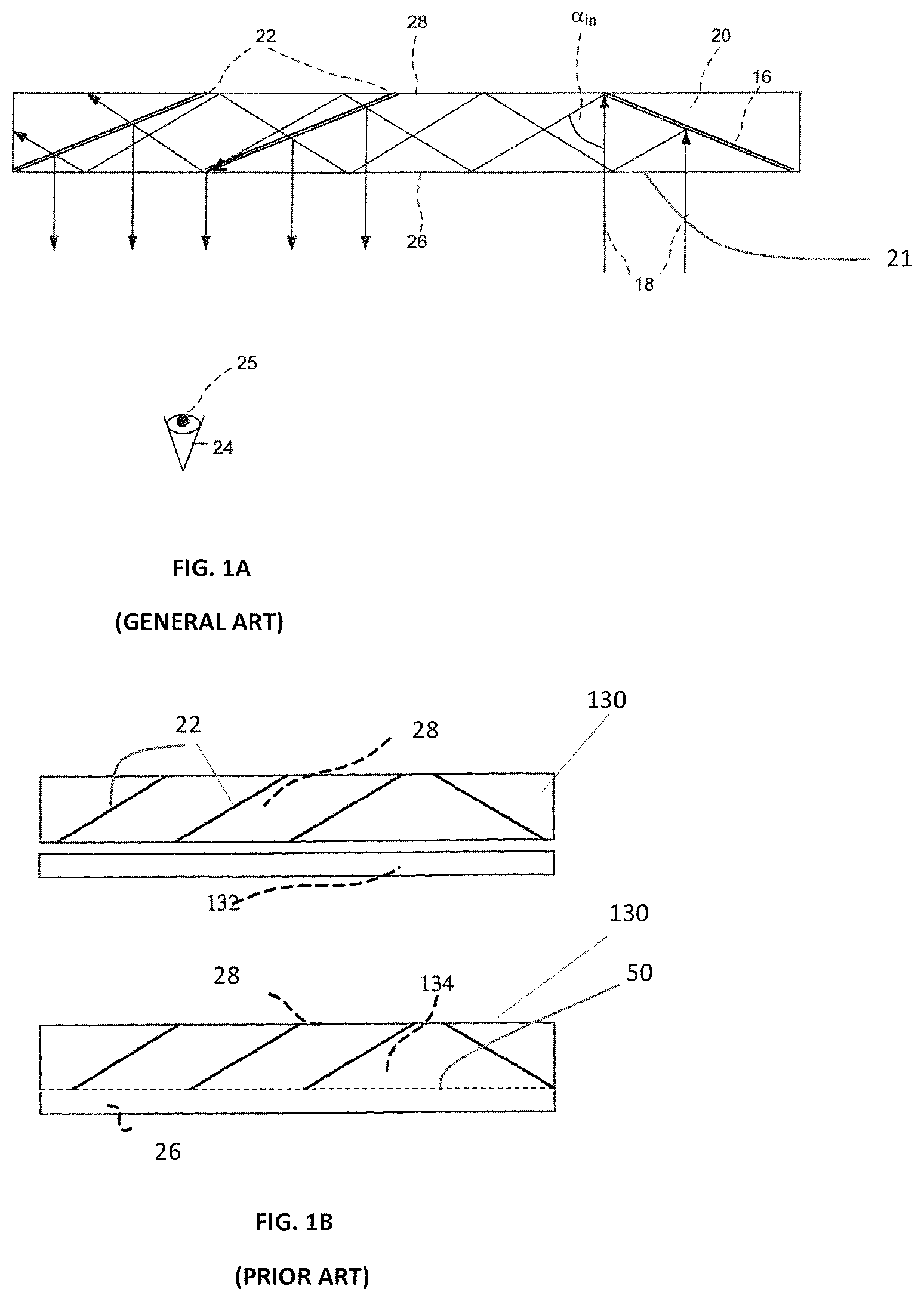
Such LOE and light propagation scheme therein and out thereof is generally illustrated in FIG. 1A. The LOE 20 has a light input region 21 (e.g. being aligned with an output of a virtual image source), major surfaces 26 and 28 guiding light by total internal reflections therefrom, and one or more at least partially reflective/diffractive surfaces 22 arranged with proper orientation inside the LOE. After several reflections from the major surfaces 26, 28, the trapped light waves reach the selective partially reflecting surface(s) 22, coupling the light out of the LOE to propagate in output direction(s) towards a pupil 25 of viewer's eye 24.
Generally speaking such at least partially reflective/diffractive surface 22 embedded in the LOE's substrate serves for redirecting the light propagating in a general propagation direction through the substrate in one or more output directions. For simplicity, such surface is termed herein below as "light directing surface".
As known, for example from the above-indicated U.S. Pat. No. 7,724,443 and WO 2007/054928 assigned to the assignee of the present application, the high performance (e.g. uniform illumination) of the LOE can be provided by embedding such light directing surfaces 22 in the substrate such that they are spaced from the major surface(s) 26, 28.
As schematically shown in FIG. 1B, according to some of the techniques described in these patent publications, such configuration can be achieved by attaching a blank plate 132 (i.e. a plate with no partially reflecting surfaces) to one of the major surfaces of the light guide substrate 130 (e.g. by using optical cement), so as to yield at an LOE 134 with the appropriate active apertures for all of the reflecting surfaces. As noted above, the two major surfaces, 26 and 28, are parallel to each other in such a way that the combined structure forms a complete rectangular parallelepiped.
As shown schematically in FIG. 1C, according to alternative techniques known from these patent publications, the same can be achieved by fabricating two similar, tooth-shaped transparent forms 140 fabricated by injection-molding or casting. The required reflecting surfaces 22 (either anisotropic or coated thin-film) are inserted in the appropriate places between the forms 140 and the two forms are then glued together to create the required LOE 144.
As seen in the figures, the resulting structure 134 (FIG. 1B) has interface 50 located in a plane parallel to the major surfaces and thus inclined with respect to the reflecting surfaces 22; and the resulting structure 144 (FIG. 1C) has an interface 150 having regions/segments 150A located in planes substantially parallel to the reflecting surfaces 22 and regions/segments 150B located in planes intersecting those of the reflecting surfaces and the major surfaces.
Generally, in order to achieve an undistorted image having good optical quality, the major and the (partially) reflecting/diffractive surfaces should have high quality. On the other hand, it is desired that the fabrication process of such LOE is as simple and straightforward as possible, as well as cost effective.
The present invention provides a novel approach for the fabrication of an LOE with one or more at least partially reflecting/diffractive surfaces (at times referred to herein below as "light directing surfaces") coupling light out of the LOE's substrate/body, and a resulting novel configuration of the LOE.
Thus, according to one broad aspect of the invention, it provides a light guide optical element (LOE) comprising: an optically transparent body which has major surfaces for guiding input light in a general propagation direction through the body by total internal reflections of light from said major surfaces, and carries at least one light directing surface, each light directing surface being configured for coupling the input light out of the body towards one or more output directions. The configuration is such that each of said at least one light directing surface is fully embedded in a volume of said body such that it is spaced from the major surfaces; and the body comprises one or more interfaces inside the body, where all of said one or more interfaces inside the body are located in at least one plane parallel to each of said at least one light directing surface and inclined with respect to said major surfaces at a predetermined angle, said at least one light directing surface being located in at least one region, respectively, at one of said one or more interfaces.
It should be understood, that in the LOE of the invention there are no interfaces other than those parallel to the light directing surfaces and extending between the major surfaces, and all the light directing surfaces are arranged in regions of at least some of such interfaces. In this connection, it should be understood that the term "interface" used herein refers to a physical boundary between elements forming an integral structure of the LOE.
In some embodiments, the body (substrate) of the LOE comprises an inner pattern formed by an array of two or more of the light directing surfaces arranged in a spaced-apart parallel relationship along at least one axis. The light directing surfaces of the array are located at the one or more interfaces inside the body and are fully embedded in the volume thereof such that the two or more light directing surfaces are spaced from the major surfaces.
At least some of such multiple light directing surfaces may be substantially equally spaced from the at least one of the major surfaces; as well as at least some of the multiple light directing surfaces may be of different or same dimensions, while differently spaced from the major surfaces.
It also should be noted that, although the invention is described below as using light directing surfaces being at least partially reflective/diffractive with respect to the input light propagating in the body, the principles of the invention are not limited to these specific applications. Thus, generally, the light directing surfaces have optical properties different from their surroundings, and may generally include surfaces having different optical properties differently affecting the input light propagating though the body (e.g. inducing polarization effect, spectral effect, etc.).
In some embodiments, the multiple light directing surfaces of the LOE are arranged in a spaced-apart relationship along two perpendicular axes in said at least one plane.
The present invention provides a novel method for fabricating the above-described LOE. Moreover, the method of the invention is advantageous for mass production of such LOEs, as is provides a simple technique for concurrently manufacturing multiple LOEs using any known suitable patterning technique(s).
Thus, according to another broad aspect of the invention, it provides a method for fabrication of two or more light guide optical elements (LOEs) configured as described above, the method comprising:
preparing at least one patterned substrate, the patterned substrate having an optically transparent planar body with a surface thereof formed with a pattern of spaced apart, parallel, light directing regions, which are arranged in an X-Z plane in a spaced-apart relationship along one of X-axis and Z-axis with optically transparent spacer regions between them;
enclosing said at least one patterned substrate between top and bottom optically transparent substrates, thereby forming a stack of multiple optically transparent layers stacked one on top of the other along Y-axis, where the pattern of the spaced apart, parallel, light directing regions is located at an interface between the layers;
dicing said stack of multiple optically transparent layers along a dicing plane intersecting with the X-Z plane and forming a predetermined angle with the X-Z plane, into a predetermined number of slices spaced from one another along the X-axis, to thereby define a plurality of bodies for the LOEs, each of said bodies comprising the at least one light directing region which is fully embedded in the LOE's body such that said at least one light directing region is spaced from major surfaces of the LOE and forms with said major surfaces said predetermined angle.
The method further comprises applying edge cutting to each of said slices producing the LOE having the optically transparent body having major surface and comprising the at least one light directing surface embedded in the body spaced from the major surfaces.
In some embodiments, where each of the LOEs to be fabricated should include multiple light directing regions, more than one patterned substrates are provided being placed one on top of the other along the Y-axis and being all enclosed between the top and bottom layers, such that the patterns of said patterned substrates are located at interfaces between the adjacent layers and are shifted with respect to one another along one of X-axis and Z-axis, thereby forming said plurality of the LOEs, each LOE comprising an inner pattern comprising two or more spaced-apart light directing regions fully embedded in the body.
It should be noted that, in some embodiments, the shift value is smaller than a minimal spacer/uncoated region between the adjacent light directing regions in the layer.
The above shift of the patterns in the adjacent layers can be achieved by properly applying the patterning process; or by shifting the similarly patterned substrates with respect to one another along X-axis.
The dimensions of the spacer regions and the dicing of the stack into the slices define distance(s) of the light directing region(s) from the major surfaces of the LOE. The two or more light directing regions may include regions of different dimensions, as well as may include regions having different optical properties differently affecting the input light.
The patterned layers may be of the same or different thicknesses.
As indicated above, the patterned substrate may be prepared by any known suitable technique, e.g. a lithography process (negative or positive patterning) creating the pattern of the spaced apart, parallel, light directing regions spaced by optically transparent spacer regions; or applying to a surface of the optically transparent planar body a direct writing patterning process.
It should be understood that, in some cases, an intermediate structure formed by the above-described stack of multiple optically transparent layers where one or more of the layers have the surface pattern, can be produced, and supplied to a customer for further slicing into LOE bodies, when needed.
The invention, in its yet further broad aspect provides such an optical structure prepared for forming therefrom multiple LOE's bodies. The optical structure is configured as a stack of multiple optically transparent layers, wherein:
each of said optically transparent layers has a surface pattern of parallel light directing regions which are arranged in an X-Z plane in a spaced-apart relationship along at least X-axis with optically transparent space regions between them;
the multiple layers are stacked one on top of the other along Y-axis such that each of the surface patterns is located at an interface between two adjacent layers and the patterns of said layers are aligned with a shift of a predetermined value along one of the X-axis and Z-axis,
thereby enabling dicing of the optical structure, along a dicing plane intersecting with a X-Z plane and forming a predetermined angle with the X-Z plane, into a predetermined number of slices spaced along one of the X-axis and Z-axes, to produce a plurality of bodies for the LOE elements, each of said bodies being formed with an inner pattern comprising an array of spaced-apart, parallel, light directing regions fully embedded in the LOE's body and being inclined with respect to surfaces of the LOE body, configured for major reflecting surfaces, with said predetermined angle.
As indicated above, the multiple layers may include two or more layers of different thicknesses.
The light directing regions of the pattern may be arranged in spaced-apart relationship along both the X-axis and Z-axis.
The invention also provides a light guide optical element (LOE) comprising an optically transparent body comprising major surfaces and configured for guiding input light in a general propagation direction through the body by total internal reflections of light from said major surfaces, and carrying at least one light directing surface configured for coupling said input light out of the body towards one or more output directions and being fully embedded in a volume of said body such that it is spaced from the major surfaces, the LOE being manufactured by a method comprising:
preparing at least one patterned substrate having an optically transparent planar body with a surface thereof formed with a pattern of spaced apart, parallel, light directing regions, which are arranged in an X-Z plane in a spaced-apart relationship along one of X-axis and Z-axis with optically transparent regions of the substrate between them;
enclosing said at least one patterned substrate between top and bottom optically transparent substrates, thereby forming a stack of multiple optically transparent layers stacked one on top of the other along Y-axis, where the pattern of the spaced apart, parallel, light directing regions is located at an interface between the layers;
dicing said stack of multiple optically transparent layers along a dicing plane intersecting with an X-Z plane and forming a predetermined angle with said X-Z plane, into a predetermined number of slices spaced from one another along said one of the X-axis and Z-axis, to thereby define a plurality of bodies for the LOEs, each of said bodies comprising the at least one light directing region which is fully embedded in the LOE's body
BRIEF DESCRIPTION OF THE DRAWINGS
In order to better understand the subject matter that is disclosed herein and to exemplify how it may be carried out in practice, embodiments will now be described, by way of non-limiting examples only, with reference to the accompanying drawings, in which:
FIG. 1A schematically illustrate the configuration and operation of a convention planar light-guide optical element (LOE) of the type to which the present invention relates;
FIGS. 1B and 1C show two known examples of the LOW configuration aimed at solving the problem associated with the conventional LOW configuration of FIG. 1A;
FIG. 2 shows schematically the configuration of the LOE according to the present invention;
FIGS. 3A-3D show an example of a method of the invention for fabrication of the multiple LOEs, each configured with a single light directing region embedded in the LOE's body;
FIGS. 4A-4E show another example of a method of the invention for fabrication of the multiple LOEs, each configured with a plurality of the spaced-apart light directing regions embedded in the LOE's body, by stacking multiple patterned substrates where the regions in each substrate extend along the Z-axis and are spaced along the X-axis, and the patterns in the stacked substrates are shifted along the X-axis;
FIG. 4F exemplifies the LOE fabricated by the general method of FIGS. 4A-D, but using different patterned layers, such that multiple light directing surfaces in the LOE include light directing surfaces having different dimensions and being differently spaced from at least one of the major surfaces;
FIGS. 5A to 5G show yet another example of a method of the invention for fabrication of the multiple LOEs, each configured with a plurality of the spaced-apart light directing regions embedded in the LOE's body, by stacking multiple patterned substrates where the regions in each substrate extend along the Z-axis and are spaced along the X-axis, and the patterns in the stacked substrates are shifted along the Z-axis;
FIGS. 6A to 6F show yet further example of a method of the invention for fabrication of the multiple LOEs, each configured with a plurality of the spaced-apart light directing regions embedded in the LOE's body, by stacking multiple patterned substrates where the regions in each substrate extend along the Z-axis and are spaced along both the X-axis and the Z-axis, and the patterns in the stacked layers are shifted along the X-axis; and
FIG. 7 illustrates a spectacles configured in which the lenses incorporate the LOEs of the invention.
DETAILED DESCRIPTION OF EMBODIMENTS
As described above, FIG. 1A illustrates schematically the configuration and operation (light propagation scheme) in a conventional LOE device, and FIGS. 1B and 1C show two examples of the improved LOE configuration providing that the light directing surfaces are fully embedded in substrate of the LOE device, being spaced from the major surface(s) thereof.
Reference is now made to FIG. 2 which schematically illustrates a part of an LOE device 200 configured according to the present invention. To facilitate understanding, the same reference numbers are used for identifying components that are common in all the examples of the invention and those of the known device described above.
The LOE 200 includes an optically transparent body 20 which has two major surfaces 26 and 28 and one or more light directing surface 22. The LOE's is thus configured for guiding input light in a general propagation direction D through the body by total internal reflections of light from the major surfaces 26 and 28, and interaction of the so-propagating light with the light directing surface(s) 22 couples the light out of the body towards one or more output directions. The LOE 200 is preferably configured such that all of the light directing surface(s) 22 are fully embedded in the volume of the body 20 being spaced (equally or not) from the major surfaces. The LOE 200 is manufactured such that the body 20 includes one or more internal interfaces, generally at 60, where each internal interface extends between the major surfaces, and where all the interfaces (in the simplest case there may be only one such interface) are located in planes parallel to that/those of the light directing surface(s) 22, and the light directing surface(s) 22 is/are located in region(s), respectively, such one or more interfaces 60.
The following are several examples of a fabrication method of the invention for fabricating the LOE device of the invention. The simplest example of concurrent manufacture of multiple bodies for LOEs, where each LOEs includes a single light directing region, is shown in FIGS. 3A-3D; and more practical examples for concurrent manufacture of multiple LOE's bodies where each LOE includes an array of two or more light directing surfaces 22 arranged in an X-Z plane in a spaced-apart parallel relationship along one of the X-axis and Z-axis (the light directing regions may be elongated extending along the Z-axis) are described below with reference to FIGS. 4A-4E, 5A-5G and 6A-6F.
As shown in FIG. 3A, a patterned substrate 70 is prepared. The patterned substrate 70 has an optically transparent planar body 20 with at least one surface pattern 72A on at least one of its surfaces 70A. It should be understood, although not specifically shown, that the opposite surface 70B may also be provided with a surface pattern. The pattern 72A is in the form of an array of spaced apart, parallel, light directing regions 22 (generally at least two such regions) spaced by optically transparent regions 74 of the substrate 20. Typically, the regions 22 and 74 are, respectively, coated by desired light directing material (e.g. at least partially reflective or diffractive) and transparent regions (i.e., not configured to cause redirecting of light) which are typically uncoated. The transparent regions are referred to herein according to a preferred embodiment as "uncoated", but it should be understood that this does not preclude implementations in which various coatings or layers are present at the transparent regions which, after bonding with suitable index-matched optical cement or other optical bonding techniques, maintain the required transparency of the transparent regions. The light directing regions 22 in this example are elongated extending along the Z-axis, and are arranged in a spaced-apart relationship along the X-axis with optically transparent uncoated regions 74 between them. The surface pattern 72A may be created using any known suitable techniques, such as lithography (negative or positive), direct writing, etc., following or preceding with an optical coating process.
It should be noted, and will described more specifically further below that the light directing regions 22 may be arranged in a two-dimensional array, i.e. light directing regions may be spaced apart along both the X- and Z-axes.
Then, the patterned substrate 70 is enclosed between optically transparent layers 76 (or at least the patterned surface 70A is covered by such layer 76). Thus, a multi-layer stack 80 is created, by gluing with an optical adhesive, including optically transparent layers (substrates) 20, 76 stacked one on top of the other along the Y-axis, where the pattern 72A of the light directing regions 22 is located at an interface 50 between the layers. As noted above, the configuration may be such that another surface pattern is made on surface 70B and is thus located at an interface between surface 70B and the other optically transparent layer 76.
Then, a dicing/cutting is applied to the stack 80 (FIG. 3C) along dicing planes 82 which intersect with the X-Z plane at predetermined angle and pass through the optically transparent uncoated regions 74. By this a plurality of LOE's bodies 20 are fabricated--11 such bodies in the present example, only one of which being shown in FIG. 3D. Each such LOE has one light directing region 22 fully embedded in the LOE's body 20 and forming said angle with the major surfaces. As shown, such LOE has no internal interfaces other than interface 50 which is located in a plane parallel to the light directing surface 22 and said light directing surface is located on a region of the interface 50 while being spaced from the outer surfaces of the body 22.
These outer major surfaces may than be further processed by the application of a various coatings including, but not limited to, Hard Coating (HC), Anti-scratch coating, super-hydrophobic coating, anti-smudge coating, anti-bacterial and anti-fouling coating, Anti-reflection coating, to create the major reflective surfaces of the LOE. Methods for the creating these coatings may include but are not limited to, liquid/solvent based coating such as dip coating, spin coating, spray-coating, die coating, capillary coating, roll coating, curtain/knife coating, bar-coating, or various printing technique, and may further include a curing step (e.g. UV/Electron beam/Thermal curing) and an additional polishing step. Alternatively, dry coatings like evaporation or sputtering of optical coatings might be applied. It should also be noted, although not specifically shown here, that an edge cutting process can be applied to each body resulting from the dicing process, thereby producing the LOE of the desired configuration to guiding input light in a general propagation direction by total internal reflections from the major surfaces and coupling light out of the LOE by interaction with the light directing surface.
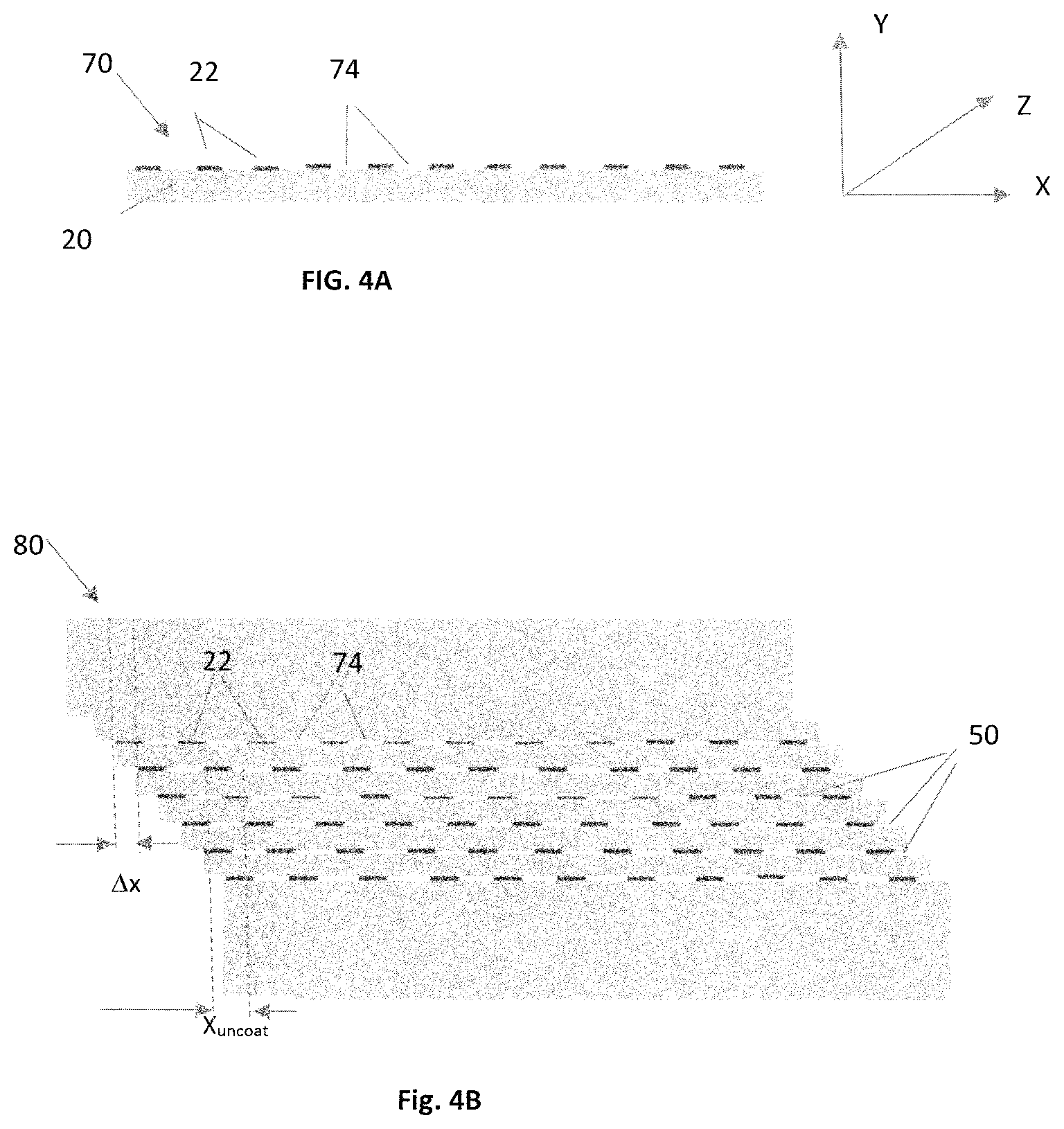
As mentioned above, the method of the invention can advantageously be used for concurrent manufacture of a large number of LOEs, each including an array of light directing surfaces. One of such method is exemplified in FIGS. 4A-4E. In this example, the method starts from preparation of the patterned substrates 70 (FIG. 4A) generally similar to the substrate of FIG. 3A. The substrates are prepared using any known suitable patterning technique.
The patterned substrates 70 are optically bonded along the Y-axis with an optical adhesive in an aligned manner one on top of the other (FIG. 4B), and may be enclosed between top and bottom optically transparent layers or only uppermost patterned surface may be covered by an optically transparent layer. By this, a multi-layer stack 80 is fabricated. In such stack 80, the patterns 72 are located at interfaces between the adjacent layers. Also, in such stack, the patterns 72 located in different planes are shifted with respect to one another along the X-axis with a predetermined shift value .DELTA.x. The shift value .DELTA.x is smaller than the minimal X-dimension, X.sub.uncoat, of the uncoated optically transparent region 74 between the adjacent light directing regions 22 in the layer. Such shifted-patterns' configuration can be obtained by either preparing the patterned layers with the required shift of the patterns, or by stacking the similarly patterned layers with the required lateral shift.
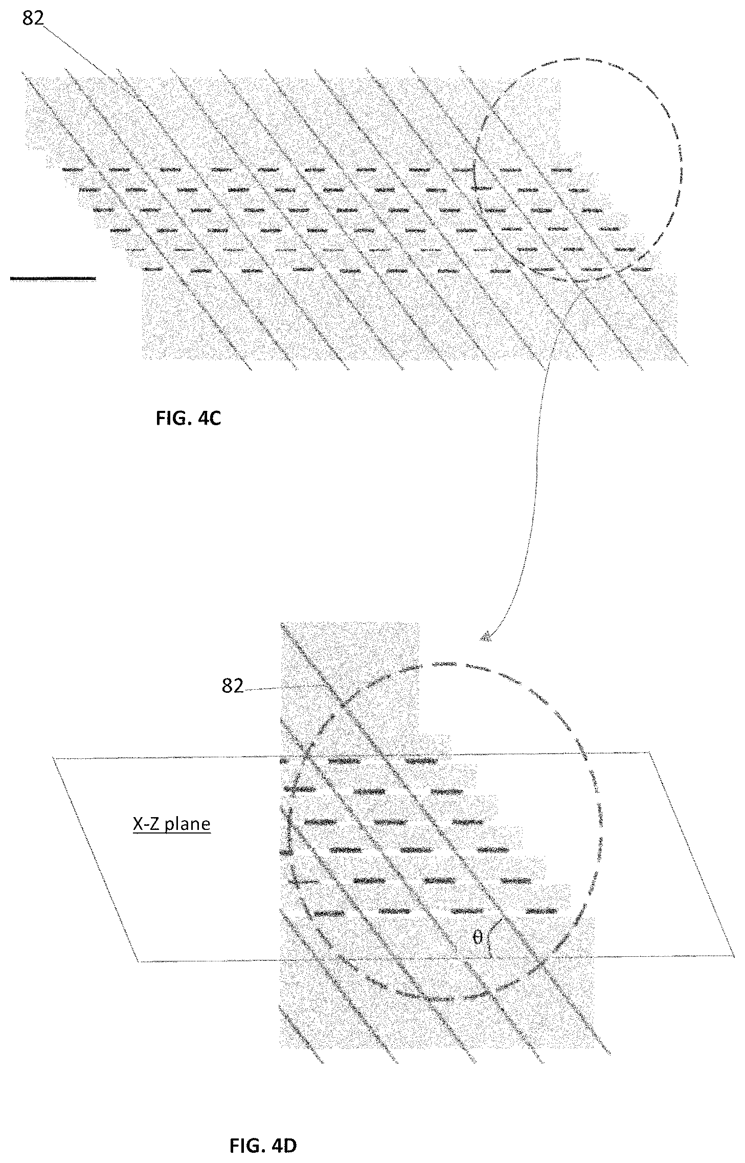
Then, the above-described dicing/cutting process is applied to the multi-layer stack 80 (FIGS. 4C and 4D) along dicing planes 82 which intersect with the X-Z plane forming a predetermined angle .theta. with the X-Z plane (as shown in FIG. 4D) and pass through the spacer regions 74 in all the patterned layers. This process results in the multiple LOE's bodies, each configured as shown in FIG. 4E, being formed with the multiple light directing regions 22 all fully embedded in the body 20 such that they are spaced from the major surfaces and are oriented with the angle .theta. with respect to the major surfaces. Also, the edge cutting process can be applied, either to the entire stack 80, or separately to each LOE body resulting from the dicing process.
It should be understood that the dimensions of the spacer/uncoated regions 74 between the light directing regions 22, as well as the parameters of the dicing applied to the stack, define distance(s) of the light directing regions 22 from the major surfaces of the LOE. As exemplified in FIG. 4F, the configuration may be such that the light directing regions 22 in the LOE 20 include regions of the same or different dimensions, as well as regions that are equally or differently spaced from the major surfaces.
FIGS. 5A to 5G show another example of a method of the invention for fabrication of the multiple LOEs, each having an array of light directing regions. First, multiple patterned substrates are prepared, one such patterned substrate 70 being shown in FIG. 5A. The patterned substrate has an optically transparent planar body 20 with a surface pattern 72A on at least one surfaces 70A. As mentioned above, the opposite surface of the substrate may also be provided with a surface pattern. The pattern 72A is in the form of two or more spaced apart, parallel, light directing regions 22 (regions coated with the required light redirecting material, such as reflective, partially reflective, or diffractive material) spaced by optically transparent (uncoated) regions 74 along the X-axis. In this example, the light directing 22 regions are elongated (lines) extend along the Z-axis. The surface pattern 72A may be created using any known suitable techniques, such as lithography (negative or positive), direct writing, etc., following or preceding with an optical coating process.
Multiple patterned substrates 70 are prepared to be enclosed between top and bottom optically transparent layers/plates 76 (FIG. 5B). The patterned substrates 70 are then stacked using an optical adhesive in an aligned manner one on top of the other along the Y-axis (FIG. 5C), and enclosed between the top and bottom optically transparent unpatterned plates 76 (or only the uppermost patterned surface may be covered by an optically transparent plate 76). By this, a multi-layer stack 80 is fabricated. In such stack 80, the patterns 72 (light directing regions) are located at the interfaces 50 between the adjacent layers. Also, in such stack 80, the substrates are shifted with respect to one another along the Z-axis with a predetermined shift value .DELTA.z.
A dicing/cutting process being applied to the multi-layer stack 80 is shown in FIG. 5D. As shown, the dicing planes 82 intersect with the X-Z plane forming a predetermined angle with the X-Z plane (as described above with reference to FIG. 4D). This process results in multiple LOE substrates--one such substrate 20 being shown in FIG. 5E. This substrate has two arrays 78A and 78B of light directing regions embedded therein (generally, two or more arrays, depending on the pattern in each initial substrate 70), where the light directing regions in the array are arranged in a spaced-apart relationship along the Z-axis, and the two arrays are arranged with a space 84 between them along the X-axis. A further dicing/cutting stage may optionally be applied to the space region 84 in such multi-array substrate (FIG. 5F), in order to obtain two LOE bodies 20A and 20B, containing respectively arrays 78A and 78B of the embedded light directing regions. In implementations of the present invention in which dicing is performed on two non-parallel planes, at least one of the dicing planes preferably passes through the transparent regions so as not to intersect the light directing regions so that the light directing regions are spaced inwards from the outer surface in the corresponding dimension of the LOE. In the present example, dicing planes 82 do intersect embedded light directing regions 78A and 78B, but the dicing plane of FIG. 5F does not. In this case, the light directing regions are not "fully embedded", as described in the following embodiments, but are inwardly spaced from the external surfaces of the LOE in at least one dimension. As shown in FIG. 5G, each of the so-obtained LOE's substrates/bodies further undergoes edge cutting and polishing. The light directing regions 22 are located within interfaces 50 oriented at the angle .theta. with respect to major surface 26 and 28, and regions 22 are appropriately spaced from the major surfaces.
It should be understood that the cutting process of FIG. 5F can alternatively be applied to the entire stack 80 of FIG. 5C, prior to the dicing process exemplified in FIG. 5D (i.e. dicing along planes 82). In this case, the dicing of FIG. 5D would be applied twice, separately to the each of two so-obtained single-array stacks.
Reference is now made to FIGS. 6A to 6F showing yet further example of a method of the invention for concurrent fabrication of the multiple LOEs, each with multiple light directing regions. This example is actually an alternative to that of FIGS. 5A-5G.
FIG. 6A shows one of a multiple patterned substrates 70. However, in this example, a patterned surface (generally, at least one surface) of the substrate 70 has a pattern in the form of a two-dimensional array of light directing regions arranged in a spaced-apart relationship along both the X-axis and the Z-axis. As described above, the light directing regions are coated by desired light directing material and are spaced by uncoated regions of the substrate. Thus, the pattern may be described as being formed by two arrays 72A and 72B of regions 22, where the arrays are spaced along the Z-axis, and the regions 22 of each array are spaced-apart along the X-axis.
Multiple patterned substrates 70 are prepared and put one on top of the other such that the patterns of different substrates are shifted with respect to one another along the X-axis a predetermined shift value .DELTA.x, as shown in FIG. 6B. The shift value .DELTA.x is smaller than the minimal X-dimension, X.sub.uncoat, of the uncoated optically transparent region 74 between the adjacent light directing regions 22 in the layer. It should be understood that in order to obtain such shift between the patterns, either the initially prepared substrates have shifted patterns, or the similarly patterned substrates are stacked with such shift, or both techniques are used.
The patterned substrates are optically bonded with an optical adhesive in an aligned manner one on top of the other to form a stack 80 (FIG. 6C), and may be enclosed between top and bottom optically transparent layers 76 (or only covered by the uppermost layer). In such stack 80, the patterns (light directing regions 22) are located at interfaces 50 between the adjacent layers/substrates.
A dicing/cutting process, similar to that described above with respect to FIGS. 3C and 4C, is applied to the multi-layer stack 80 (FIG. 6D) along dicing planes 82 which intersect with the X-Z plane forming a predetermined angle .theta. therewith as described above. The resulting LOE body 20, being one of the multiple bodies, is shown in FIG. 6E, and after the edge cutting and polishing process--is shown in FIG. 6F. As described above, in this example, the dicing/cutting along the X-axis in the space between the two arrays, might be first applied to the stack 80 and then the dicing along planes 82 may be applied to each of the resulting half-stacks. Each LOE body 20 has multiple spaced-apart parallel light directing regions all fully embedded in the body such that they are spaced (equally or not) from the surfaces 26 and 28 that are to serve as major surfaces.
It should be understood that the LOE produced by the methods of the invention (FIGS. 3D, 4E, 5G and 6F) has no internal interfaces other than interfaces 50 which are located in a plane parallel to the light directing surface 22 and said light directing surfaces are located in regions of the interfaces 50, while being spaced from the external surfaces of the body 22 in at least one dimension, and in particularly preferred cases, being spaced from the surfaces to be used as the major reflective surfaces of body 22.
FIG. 7 exemplifies how the structure (LOE) of the invention can be incorporated in spectacles. Each lens in the spectacles is formed as or carries the LOE attached thereto, and, when used together with a virtual image source, the light directing surfaces directs virtual image light towards the wearer's eye.
* * * * *
D00000
D00001
D00002
D00003
D00004
D00005
D00006
D00007
D00008
D00009
D00010
XML
uspto.report is an independent third-party trademark research tool that is not affiliated, endorsed, or sponsored by the United States Patent and Trademark Office (USPTO) or any other governmental organization. The information provided by uspto.report is based on publicly available data at the time of writing and is intended for informational purposes only.
While we strive to provide accurate and up-to-date information, we do not guarantee the accuracy, completeness, reliability, or suitability of the information displayed on this site. The use of this site is at your own risk. Any reliance you place on such information is therefore strictly at your own risk.
All official trademark data, including owner information, should be verified by visiting the official USPTO website at www.uspto.gov. This site is not intended to replace professional legal advice and should not be used as a substitute for consulting with a legal professional who is knowledgeable about trademark law.