Memcached server functionality in a cluster of data processing nodes
Davis , et al. December 29, 2
U.S. patent number 10,877,695 [Application Number 16/198,619] was granted by the patent office on 2020-12-29 for memcached server functionality in a cluster of data processing nodes. This patent grant is currently assigned to III Holdings 2, LLC. The grantee listed for this patent is III Holdings 2, LLC. Invention is credited to Prashant R. Chandra, Mark Bradley Davis.


View All Diagrams
| United States Patent | 10,877,695 |
| Davis , et al. | December 29, 2020 |
Memcached server functionality in a cluster of data processing nodes
Abstract
A method is performed by a first server on a chip (SoC) node that is one instance of a plurality of nodes within a cluster of nodes. An operation is performed for determine if a second one of the SoC nodes in the cluster has data stored thereon corresponding to a data identifier in response to receiving a data retrieval request including the data identifier. An operation is performed for determining if a remote memory access channel exists between the SoC node and the second one of the SoC nodes. An operation is performed for access the data from the second one of the SoC nodes using the remote memory access channel after determine that the second one of the SoC nodes has the data stored thereon and that the remote memory access channel exists between the SoC node and the second one of the SoC nodes.
| Inventors: | Davis; Mark Bradley (Austin, TX), Chandra; Prashant R. (San Jose, CA) | ||||||||||
|---|---|---|---|---|---|---|---|---|---|---|---|
| Applicant: |
|
||||||||||
| Assignee: | III Holdings 2, LLC
(Wilmington, DE) |
||||||||||
| Family ID: | 1000005269768 | ||||||||||
| Appl. No.: | 16/198,619 | ||||||||||
| Filed: | November 21, 2018 |
Prior Publication Data
| Document Identifier | Publication Date | |
|---|---|---|
| US 20200159449 A1 | May 21, 2020 | |
Related U.S. Patent Documents
| Application Number | Filing Date | Patent Number | Issue Date | ||
|---|---|---|---|---|---|
| 15357332 | Nov 27, 2018 | 10140245 | |||
| 13728428 | May 9, 2017 | 9648102 | |||
| 13453086 | Dec 3, 2013 | 8599863 | |||
| 12794996 | Jun 7, 2010 | ||||
| 61256723 | Oct 30, 2009 | ||||
| Current U.S. Class: | 1/1 |
| Current CPC Class: | G06F 3/067 (20130101); G06F 3/0659 (20130101); G06F 3/0604 (20130101); H04L 67/2842 (20130101) |
| Current International Class: | G06F 3/06 (20060101); H04L 29/08 (20060101) |
References Cited [Referenced By]
U.S. Patent Documents
| 5451936 | September 1995 | Yang et al. |
| 5594908 | January 1997 | Hyatt |
| 5623641 | April 1997 | Kadoyashiki |
| 5781187 | July 1998 | Gephardt et al. |
| 5901048 | May 1999 | Hu |
| 5908468 | June 1999 | Hartmann |
| 5968176 | October 1999 | Nessett et al. |
| 5971804 | October 1999 | Gallagher et al. |
| 6055618 | April 2000 | Thorson |
| 6141214 | October 2000 | Ahn |
| 6181699 | January 2001 | Crinion et al. |
| 6192414 | February 2001 | Horn |
| 6198741 | March 2001 | Yoshizawa et al. |
| 6252878 | June 2001 | Locklear, Jr. et al. |
| 6314487 | November 2001 | Hahn et al. |
| 6314501 | November 2001 | Gulick et al. |
| 6373841 | April 2002 | Goh et al. |
| 6442137 | August 2002 | Yu et al. |
| 6446192 | September 2002 | Narasimhan et al. |
| 6452809 | September 2002 | Jackson et al. |
| 6507586 | January 2003 | Satran et al. |
| 6556952 | April 2003 | Magro |
| 6574238 | June 2003 | Thrysoe |
| 6661671 | December 2003 | Franke et al. |
| 6711691 | March 2004 | Howard et al. |
| 6766389 | July 2004 | Hayter et al. |
| 6813676 | November 2004 | Henry et al. |
| 6816750 | November 2004 | Klaas |
| 6842430 | January 2005 | Melnik |
| 6857026 | February 2005 | Cain |
| 6963926 | November 2005 | Robinson |
| 6963948 | November 2005 | Gulick |
| 6977939 | December 2005 | Joy et al. |
| 6988170 | January 2006 | Barroso et al. |
| 6990063 | January 2006 | Lenoski et al. |
| 7020695 | March 2006 | Kundu et al. |
| 7032119 | April 2006 | Fung |
| 7080078 | July 2006 | Slaughter et al. |
| 7080283 | July 2006 | Songer et al. |
| 7095738 | August 2006 | Desanti |
| 7119591 | October 2006 | Lin |
| 7143153 | November 2006 | Black et al. |
| 7165120 | January 2007 | Giles et al. |
| 7170315 | January 2007 | Bakker et al. |
| 7180866 | February 2007 | Chartre et al. |
| 7203063 | April 2007 | Bash et al. |
| 7257655 | August 2007 | Burney et al. |
| 7263288 | August 2007 | Islam |
| 7274705 | September 2007 | Chang et al. |
| 7278582 | October 2007 | Siegel et al. |
| 7310319 | December 2007 | Awsienko et al. |
| 7325050 | January 2008 | O'Connor et al. |
| 7337333 | February 2008 | O'Conner et al. |
| 7340777 | March 2008 | Szor |
| 7353362 | April 2008 | Georgiou et al. |
| 7382154 | June 2008 | Ramos et al. |
| 7386888 | June 2008 | Liang et al. |
| 7418534 | August 2008 | Hayter et al. |
| 7437540 | October 2008 | Paolucci et al. |
| 7447147 | November 2008 | Nguyen et al. |
| 7447197 | November 2008 | Terrell et al. |
| 7466712 | December 2008 | Makishima et al. |
| 7467306 | December 2008 | Cartes et al. |
| 7467358 | December 2008 | Kang et al. |
| 7502884 | March 2009 | Shah et al. |
| 7519843 | April 2009 | Buterbaugh et al. |
| 7555666 | June 2009 | Brundridge et al. |
| 7583661 | September 2009 | Chaudhuri |
| 7586841 | September 2009 | Vasseur |
| 7596144 | September 2009 | Pong |
| 7599360 | October 2009 | Edsall et al. |
| 7606225 | October 2009 | Xie et al. |
| 7606245 | October 2009 | Ma et al. |
| 7616646 | November 2009 | Ma et al. |
| 7620057 | November 2009 | Aloni et al. |
| 7644215 | January 2010 | Wallace et al. |
| 7657677 | February 2010 | Huang et al. |
| 7657756 | February 2010 | Hall |
| 7660922 | February 2010 | Harriman |
| 7664110 | February 2010 | Lovett et al. |
| 7673164 | March 2010 | Agarwal |
| 7710936 | May 2010 | Morales Barroso |
| 7719834 | May 2010 | Miyamoto et al. |
| 7721125 | May 2010 | Fung |
| 7751433 | July 2010 | Dollo et al. |
| 7760720 | July 2010 | Pullela et al. |
| 7761687 | July 2010 | Blumrich et al. |
| 7783910 | August 2010 | Felter et al. |
| 7791894 | September 2010 | Bechtolsheim |
| 7792113 | September 2010 | Foschiano et al. |
| 7796399 | September 2010 | Clayton et al. |
| 7801132 | September 2010 | Ofek et al. |
| 7802017 | September 2010 | Uemura et al. |
| 7805575 | September 2010 | Agarwal et al. |
| 7831839 | November 2010 | Hatakeyama |
| 7840703 | November 2010 | Arimilli et al. |
| 7865614 | January 2011 | Lu et al. |
| 7925795 | April 2011 | Tamir et al. |
| 7934005 | April 2011 | Fascenda |
| 7970929 | June 2011 | Mahalingaiah |
| 7975110 | July 2011 | Spaur et al. |
| 7991817 | August 2011 | Dehon et al. |
| 7991922 | August 2011 | Hayter et al. |
| 7992151 | August 2011 | Warrier et al. |
| 8019832 | September 2011 | De Sousa et al. |
| 8060760 | November 2011 | Shetty et al. |
| 8060775 | November 2011 | Sharma et al. |
| 8082400 | December 2011 | Chang et al. |
| 8108508 | January 2012 | Goh et al. |
| 8122269 | February 2012 | Houlihan et al. |
| 8132034 | March 2012 | Lambert et al. |
| 8155113 | April 2012 | Agarwal |
| 8156362 | April 2012 | Branover et al. |
| 8165120 | April 2012 | Maruccia et al. |
| 8170040 | May 2012 | Konda |
| 8180996 | May 2012 | Fullerton et al. |
| 8189612 | May 2012 | Lemaire et al. |
| 8194659 | June 2012 | Ban |
| 8199636 | June 2012 | Rouyer et al. |
| 8205103 | June 2012 | Kazama et al. |
| 8379425 | February 2013 | Fukuoka et al. |
| 8397092 | March 2013 | Karnowski |
| 8407428 | March 2013 | Cheriton et al. |
| 8504791 | August 2013 | Cheriton et al. |
| RE44610 | November 2013 | Krakirian et al. |
| 8599863 | December 2013 | Davis |
| 8684802 | April 2014 | Gross et al. |
| 8738860 | May 2014 | Griffin et al. |
| 8745275 | June 2014 | Ikeya et al. |
| 8745302 | June 2014 | Davis et al. |
| 8782321 | July 2014 | Harriman et al. |
| 8812400 | August 2014 | Faraboschi et al. |
| 8824485 | September 2014 | Biswas et al. |
| 8854831 | October 2014 | Arnouse |
| 8903964 | December 2014 | Breslin et al. |
| 9008079 | April 2015 | Davis et al. |
| 9075655 | July 2015 | Davis et al. |
| 9311269 | April 2016 | Davis et al. |
| 9465771 | October 2016 | Davis et al. |
| 2001/0046227 | November 2001 | Matsuhira et al. |
| 2002/0004912 | January 2002 | Fung |
| 2002/0040391 | April 2002 | Chaiken et al. |
| 2002/0083352 | June 2002 | Fujimoto et al. |
| 2002/0097732 | July 2002 | Worster et al. |
| 2002/0107903 | August 2002 | Richter et al. |
| 2002/0124128 | September 2002 | Qiu |
| 2002/0159452 | October 2002 | Foster et al. |
| 2002/0161917 | October 2002 | Shapiro et al. |
| 2002/0172205 | November 2002 | Tagore-Brage et al. |
| 2002/0186656 | December 2002 | Vu |
| 2002/0194412 | December 2002 | Bottom |
| 2002/0196611 | December 2002 | Ho et al. |
| 2003/0007493 | January 2003 | Oi et al. |
| 2003/0033547 | February 2003 | Larson et al. |
| 2003/0041266 | February 2003 | Ke et al. |
| 2003/0076832 | April 2003 | Ni |
| 2003/0093255 | May 2003 | Freyensee et al. |
| 2003/0093624 | May 2003 | Arimilli et al. |
| 2003/0110262 | June 2003 | Hasan et al. |
| 2003/0140190 | July 2003 | Mahony et al. |
| 2003/0158940 | August 2003 | Leigh |
| 2003/0159083 | August 2003 | Fukuhara et al. |
| 2003/0172191 | September 2003 | Williams |
| 2003/0188083 | October 2003 | Kumar et al. |
| 2003/0193402 | October 2003 | Post et al. |
| 2003/0202520 | October 2003 | Witkowski et al. |
| 2003/0231624 | December 2003 | Alappat et al. |
| 2004/0013113 | January 2004 | Singh et al. |
| 2004/0017806 | January 2004 | Yazdy et al. |
| 2004/0017808 | January 2004 | Forbes et al. |
| 2004/0030938 | February 2004 | Barr et al. |
| 2004/0068676 | April 2004 | Larson et al. |
| 2004/0111612 | June 2004 | Choi et al. |
| 2004/0141521 | July 2004 | George |
| 2004/0165588 | August 2004 | Pandya |
| 2004/0210693 | October 2004 | Zeitler et al. |
| 2004/0215864 | October 2004 | Arimilli et al. |
| 2004/0215991 | October 2004 | McAfee et al. |
| 2004/0267486 | December 2004 | Percer et al. |
| 2005/0015378 | January 2005 | Gammel et al. |
| 2005/0018604 | January 2005 | Dropps et al. |
| 2005/0018606 | January 2005 | Dropps et al. |
| 2005/0018663 | January 2005 | Dropps et al. |
| 2005/0021606 | January 2005 | Davies et al. |
| 2005/0021728 | January 2005 | Sugimoto |
| 2005/0030954 | February 2005 | Dropps et al. |
| 2005/0033742 | February 2005 | Kamvar et al. |
| 2005/0033890 | February 2005 | Lee |
| 2005/0044195 | February 2005 | Westfall |
| 2005/0077921 | April 2005 | Percer et al. |
| 2005/0105538 | May 2005 | Perera et al. |
| 2005/0141424 | June 2005 | Lim et al. |
| 2005/0228852 | October 2005 | Santos et al. |
| 2005/0240688 | October 2005 | Moerman et al. |
| 2005/0259397 | November 2005 | Bash et al. |
| 2006/0002311 | January 2006 | Iwanaga et al. |
| 2006/0013218 | January 2006 | Shore et al. |
| 2006/0023245 | February 2006 | Sato et al. |
| 2006/0029053 | February 2006 | Roberts et al. |
| 2006/0090025 | April 2006 | Tufford et al. |
| 2006/0136570 | June 2006 | Pandya |
| 2006/0140211 | June 2006 | Huang et al. |
| 2006/0174342 | August 2006 | Zaheer et al. |
| 2006/0179241 | August 2006 | Clark et al. |
| 2006/0236371 | October 2006 | Fish |
| 2006/0248359 | November 2006 | Fung |
| 2006/0259734 | November 2006 | Sheu et al. |
| 2006/0265609 | November 2006 | Fung |
| 2007/0006001 | January 2007 | Isobe et al. |
| 2007/0047195 | March 2007 | Merkin et al. |
| 2007/0076653 | April 2007 | Park et al. |
| 2007/0081315 | April 2007 | Mondor et al. |
| 2007/0094486 | April 2007 | Moore et al. |
| 2007/0109968 | May 2007 | Hussain et al. |
| 2007/0130397 | June 2007 | Tsu |
| 2007/0174390 | July 2007 | Silvain et al. |
| 2007/0180310 | August 2007 | Johnson et al. |
| 2007/0209072 | September 2007 | Chen |
| 2007/0226795 | September 2007 | Conti et al. |
| 2007/0280230 | December 2007 | Park |
| 2007/0286009 | December 2007 | Norman |
| 2007/0288585 | December 2007 | Sekiguchi et al. |
| 2008/0013453 | January 2008 | Chiang et al. |
| 2008/0040463 | February 2008 | Brown et al. |
| 2008/0052437 | February 2008 | Loffink et al. |
| 2008/0059782 | March 2008 | Kruse et al. |
| 2008/0075089 | March 2008 | Evans et al. |
| 2008/0089358 | April 2008 | Basso et al. |
| 2008/0104264 | May 2008 | Duerk et al. |
| 2008/0140771 | June 2008 | Vass et al. |
| 2008/0140930 | June 2008 | Hotchkiss |
| 2008/0159745 | July 2008 | Segal |
| 2008/0162691 | July 2008 | Zhang et al. |
| 2008/0183882 | July 2008 | Flynn et al. |
| 2008/0186965 | August 2008 | Zheng et al. |
| 2008/0199133 | August 2008 | Takizawa et al. |
| 2008/0212273 | September 2008 | Bechtolsheim |
| 2008/0212276 | September 2008 | Bottom et al. |
| 2008/0217021 | September 2008 | Lembcke et al. |
| 2008/0222434 | September 2008 | Shimizu et al. |
| 2008/0235443 | September 2008 | Chow et al. |
| 2008/0239649 | October 2008 | Bradicich et al. |
| 2008/0243634 | October 2008 | Dworkin et al. |
| 2008/0250181 | October 2008 | Li et al. |
| 2008/0259555 | October 2008 | Bechtolsheim et al. |
| 2008/0259788 | October 2008 | Wang et al. |
| 2008/0266793 | October 2008 | Lee |
| 2008/0270599 | October 2008 | Tamir et al. |
| 2008/0288660 | November 2008 | Balasubramanian et al. |
| 2008/0288664 | November 2008 | Pettey et al. |
| 2008/0288683 | November 2008 | Ramey |
| 2008/0301379 | December 2008 | Pong |
| 2008/0301794 | December 2008 | Lee |
| 2008/0310848 | December 2008 | Yasuda et al. |
| 2008/0313369 | December 2008 | Verdoorn et al. |
| 2008/0320161 | December 2008 | Maruccia et al. |
| 2009/0021907 | January 2009 | Mann et al. |
| 2009/0044036 | February 2009 | Merkin |
| 2009/0063443 | March 2009 | Arimilli et al. |
| 2009/0064287 | March 2009 | Bagepalli et al. |
| 2009/0080428 | March 2009 | Witkowski et al. |
| 2009/0097200 | April 2009 | Sharma et al. |
| 2009/0113130 | April 2009 | He et al. |
| 2009/0133129 | May 2009 | Jeong et al. |
| 2009/0135751 | May 2009 | Hodges et al. |
| 2009/0135835 | May 2009 | Gallatin et al. |
| 2009/0158070 | June 2009 | Gruendler |
| 2009/0172423 | July 2009 | Song et al. |
| 2009/0198958 | August 2009 | Arimilli et al. |
| 2009/0204834 | August 2009 | Hendin et al. |
| 2009/0204837 | August 2009 | Raval et al. |
| 2009/0216920 | August 2009 | Lauterbach et al. |
| 2009/0219827 | September 2009 | Chen et al. |
| 2009/0222884 | September 2009 | Shaji et al. |
| 2009/0225751 | September 2009 | Koenck et al. |
| 2009/0235104 | September 2009 | Fung |
| 2009/0248943 | October 2009 | Jiang et al. |
| 2009/0251867 | October 2009 | Sharma et al. |
| 2009/0259863 | October 2009 | Williams et al. |
| 2009/0259864 | October 2009 | Li et al. |
| 2009/0265045 | October 2009 | Coxe, III |
| 2009/0271656 | October 2009 | Yokota et al. |
| 2009/0276666 | November 2009 | Haley et al. |
| 2009/0279518 | November 2009 | Falk et al. |
| 2009/0282274 | November 2009 | Langgood et al. |
| 2009/0282419 | November 2009 | Mejdrich et al. |
| 2009/0313390 | December 2009 | Ahuja et al. |
| 2010/0005331 | January 2010 | Somasundaram et al. |
| 2010/0008038 | January 2010 | Coglitore |
| 2010/0008365 | January 2010 | Porat |
| 2010/0026408 | February 2010 | Shau |
| 2010/0040053 | February 2010 | Gottumukkula et al. |
| 2010/0049822 | February 2010 | Davies et al. |
| 2010/0051391 | March 2010 | Jahkonen |
| 2010/0106987 | April 2010 | Lambert et al. |
| 2010/0118880 | May 2010 | Kunz et al. |
| 2010/0125742 | May 2010 | Ohtani |
| 2010/0125915 | May 2010 | Hall et al. |
| 2010/0138481 | June 2010 | Behrens |
| 2010/0158005 | June 2010 | Mukhopadhyay et al. |
| 2010/0161909 | June 2010 | Nation et al. |
| 2010/0165983 | July 2010 | Aybay et al. |
| 2010/0169479 | July 2010 | Jeong et al. |
| 2010/0198972 | August 2010 | Umbehocker |
| 2010/0198985 | August 2010 | Kanevsky et al. |
| 2010/0218194 | August 2010 | Dallman et al. |
| 2010/0220732 | September 2010 | Hussain et al. |
| 2010/0250914 | September 2010 | Abdul et al. |
| 2010/0265650 | October 2010 | Chen et al. |
| 2010/0281246 | November 2010 | Bristow et al. |
| 2010/0299548 | November 2010 | Chadirchi et al. |
| 2010/0308897 | December 2010 | Evoy et al. |
| 2010/0312910 | December 2010 | Lin et al. |
| 2010/0312969 | December 2010 | Yamazaki et al. |
| 2010/0318812 | December 2010 | Auradkar et al. |
| 2011/0023104 | January 2011 | Franklin |
| 2011/0026397 | February 2011 | Saltsidis et al. |
| 2011/0029652 | February 2011 | Chhuor et al. |
| 2011/0058573 | March 2011 | Balakavi et al. |
| 2011/0075369 | March 2011 | Sun et al. |
| 2011/0090633 | April 2011 | Rabinovitz |
| 2011/0103391 | May 2011 | Davis et al. |
| 2011/0113115 | May 2011 | Chang et al. |
| 2011/0119344 | May 2011 | Eustis |
| 2011/0123014 | May 2011 | Smith |
| 2011/0138046 | June 2011 | Bonnier et al. |
| 2011/0173612 | July 2011 | El Zur et al. |
| 2011/0185370 | July 2011 | Tamir et al. |
| 2011/0191514 | August 2011 | Wu et al. |
| 2011/0191610 | August 2011 | Agarwal et al. |
| 2011/0197012 | August 2011 | Liao et al. |
| 2011/0210975 | September 2011 | Wong et al. |
| 2011/0239014 | September 2011 | Karnowski |
| 2011/0271159 | November 2011 | Ahn et al. |
| 2011/0273840 | November 2011 | Chen |
| 2011/0295991 | December 2011 | Aida |
| 2011/0296141 | December 2011 | Daffron |
| 2011/0307887 | December 2011 | Huang et al. |
| 2011/0320690 | December 2011 | Petersen et al. |
| 2012/0011500 | January 2012 | Faraboschi et al. |
| 2012/0020207 | January 2012 | Corti et al. |
| 2012/0050981 | March 2012 | Xu et al. |
| 2012/0054469 | March 2012 | Ikeya et al. |
| 2012/0054511 | March 2012 | Brinks et al. |
| 2012/0081850 | April 2012 | Regimbal et al. |
| 2012/0096211 | April 2012 | Davis et al. |
| 2012/0099265 | April 2012 | Reber |
| 2012/0131201 | May 2012 | Matthews et al. |
| 2012/0155168 | June 2012 | Kim et al. |
| 2012/0198252 | August 2012 | Kirschtein et al. |
| 2012/0207165 | August 2012 | Davis |
| 2012/0297042 | November 2012 | Davis et al. |
| 2013/0010639 | January 2013 | Armstrong et al. |
| 2013/0024645 | January 2013 | Cheriton et al. |
| 2013/0031331 | January 2013 | Cheriton et al. |
| 2013/0058250 | March 2013 | Casado et al. |
| 2013/0094499 | April 2013 | Davis et al. |
| 2013/0097448 | April 2013 | Davis et al. |
| 2013/0111107 | May 2013 | Chang et al. |
| 2013/0148667 | June 2013 | Hama et al. |
| 2013/0163605 | June 2013 | Chandra et al. |
| 2013/0275703 | October 2013 | Schenfeld et al. |
| 2013/0290643 | October 2013 | Lim et al. |
| 2013/0290650 | October 2013 | Chang et al. |
| 2013/0318269 | November 2013 | Dalal et al. |
| 2014/0122833 | May 2014 | Davis et al. |
| 2014/0359044 | December 2014 | Davis et al. |
| 2014/0365596 | December 2014 | Kanevsky et al. |
| 2015/0039840 | February 2015 | Chandra et al. |
| 2015/0103826 | April 2015 | Davis |
| 2016/0161909 | June 2016 | Wada |
| 60216001 | Jul 2007 | DE | |||
| 10 2008 001 875 | Jun 2010 | DE | |||
| 2005-223753 | Aug 2005 | JP | |||
| 2005-536960 | Dec 2005 | JP | |||
| M377621 | Apr 2010 | TW | |||
| 201017430 | May 2010 | TW | |||
| WO-2004/021641 | Mar 2004 | WO | |||
| WO-2005/013143 | Feb 2005 | WO | |||
| WO-2008/000193 | Jan 2008 | WO | |||
| WO-2011/044271 | Apr 2011 | WO | |||
| WO-2012/037494 | Mar 2012 | WO | |||
Other References
|
Advanced Switching Technology Tech Brief, published 2005, 2 pages. cited by applicant . Chapter 1 Overview of the Origin Family Architecture from Origin and Onyx2 Theory of Operations Manual, published 1997, 18 pages. cited by applicant . Cisco MDS 9000 Family Multiprotocol Services Module, published 2006, 13 pages. cited by applicant . Comparing the I2C BUS to the SMBUS, Maxim Integrated, Dec. 1, 2000, p. 1. cited by applicant . Das et al., "Unifying Packet and Circuit Switched Networks," IEEE Globecom Workshops 2009, Nov. 30, 2009, pp. 1-6. cited by applicant . Deering, "IP Multicast Extensions for 4.3BSD UNIX and related Systems," Jun. 1999, 5 pages. cited by applicant . Elghany et al., "High Throughput High Performance NoC Switch," NORCHIP 2008, Nov. 2008, pp. 237-240. cited by applicant . Extended European Search Report for EP 10827330.1, dated Jun. 5, 2013. cited by applicant . Final Office Action on U.S. Appl. No. 12/889,721, dated Apr. 17, 2014. cited by applicant . Final Office Action on U.S. Appl. No. 15/281,462, dated Apr. 6, 2018. cited by applicant . Final Office Action on U.S. Appl. No. 13/234,054, dated Jan. 26, 2016. cited by applicant . Final Office Action on U.S. Appl. No. 13/692,741, dated Mar. 11, 2015. cited by applicant . Final Office Action on U.S. Appl. No. 12/794,996, dated Jun. 19, 2013. cited by applicant . Final Office Action on U.S. Appl. No. 12/889,721 dated Aug. 2, 2016. cited by applicant . Final Office Action on U.S. Appl. No. 12/889,721, dated May 22, 2015. cited by applicant . Final Office Action on U.S. Appl. No. 13/234,054 dated May 31, 2017. cited by applicant . Final Office Action on U.S. Appl. No. 13/234,054, dated Apr. 16, 2015. cited by applicant . Final Office Action on U.S. Appl. No. 13/475,713, dated Oct. 17, 2014. cited by applicant . Final Office Action on U.S. Appl. No. 13/475,722, dated Oct. 20, 2014. cited by applicant . Final Office Action on U.S. Appl. No. 13/527,498, dated Nov. 17, 2014. cited by applicant . Final Office Action on U.S. Appl. No. 13/527,505, dated Dec. 5, 2014. cited by applicant . Final Office Action on U.S. Appl. No. 13/624,725 dated Mar. 10, 2016. cited by applicant . Final Office Action on U.S. Appl. No. 13/624,725, dated Nov. 13, 2013. cited by applicant . Final Office Action on U.S. Appl. No. 13/624,731, dated Jul. 25, 2014. cited by applicant . Final Office Action on U.S. Appl. No. 13/662,759, dated Feb. 22, 2016. cited by applicant . Final Office Action on U.S. Appl. No. 13/705,340, dated Aug. 2, 2013. cited by applicant . Final Office Action on U.S. Appl. No. 13/705,414, dated Aug. 9, 2013. cited by applicant . Final Office Action on U.S. Appl. No. 13/728,428 dated May 6, 2016. cited by applicant . Final Office Action on U.S. Appl. No. 14/052,723, dated Dec. 3, 2015. cited by applicant . Final Office Action on U.S. Appl. No. 14/106,697 dated Feb. 2, 2016. cited by applicant . Final Office Action on U.S. Appl. No. 14/106,698, dated Aug. 19, 2015. cited by applicant . Final Office Action on U.S. Appl. No. 14/334,178, dated Nov. 4, 2015. cited by applicant . Final Office Action on U.S. Appl. No. 14/334,931, dated Jul. 9, 2015. cited by applicant . Final Office Action on U.S. Appl. No. 14/809,723 dated Aug. 25, 2017. cited by applicant . Final Office Action on U.S. Appl. No. 15/281,462 dated Jun. 13, 2017. cited by applicant . Final Office Action on U.S. Appl. No. 15/357,332 dated May 9, 2018. cited by applicant . Final Office Action on U.S. Appl. No. 13/624,731, dated Nov. 12, 2013. cited by applicant . fpga4fun.com,"What is JTAG?", 2 pages, Jan. 31, 2010. cited by applicant . From AT to BTX: Motherboard Form Factor, Webopedia, Apr. 29, 2005, p. 1. cited by applicant . Grecu et al., "A Scalable Communication-Centric SoC Interconnect Architecture" Proceedings 5th International Symposium on Quality Electronic Design, 2005, pp. 343, 348 (full article included). cited by applicant . Hossain et al., "Extended Butterfly Fat Tree Interconnection (EFTI) Architecture for Network on CHIP," 2005 IEEE Pacific Rim Conference on Communicatinos, Computers and Signal Processing, Aug. 2005, pp. 613-616. cited by applicant . HP ProLiant SL6500 Scalable System, Family data sheet, HP Technical sheet, Sep. 2010 4 pages. cited by applicant . HP Virtual Connect Traffic Flow--Technology brief, Jan. 2012, 22 pages. cited by applicant . International Preliminary Report on Patentability issued on PCT/US12/62608, dated May 6, 2014. cited by applicant . International Search Report and Written Opinion for PCT/US12/38987, dated Aug. 16, 2012. cited by applicant . International Search Report and Written Opinion for PCT/US12/61747, dated Mar. 1, 2013. cited by applicant . International Search Report and Written Opinion for PCT/US12/62608, dated Jan. 18, 2013. cited by applicant . International Search Report and Written Opinion for PCT/US2010/053227, dated May 10, 2012. cited by applicant . International Search Report and Written Opinion for PCT/US2011/051996, dated Jan. 19, 2012. cited by applicant . International Search Report and Written Opinion on PCT/US09/44200, dated Jul. 1, 2009. cited by applicant . International Search Report and Written Opinion on PCT/US2012/038986, dated Mar. 14, 2013. cited by applicant . Jansen et al., "SATA-IO to Develop Specification for Mini Interface Connector" Press Release Sep. 21, 2009, Serial ATA3 pages. cited by applicant . Nawathe et al., "Implementation of an 8-Core, 64-Thread, Power Efficient SPARC Server on a Chip", IEEE Journal of Solid-State Circuits, vol. 43, No. 1, Jan. 2008, pp. 6-20. cited by applicant . Non-Final Action on U.S. Appl. No. 13/728,362, dated Feb. 21, 2014. cited by applicant . Non-Final Office Action on U.S. Appl. No. 15/281,462 dated Feb. 10, 2017. cited by applicant . Non-Final Office Action on U.S. Appl. No. 15/254,111 dated Jun. 20, 2017. cited by applicant . Non-Final Office Action on U.S. Appl. No. 14/334,178 dated Dec. 18, 2015. cited by applicant . Non-Final Office Action on U.S. Appl. No. 12/889,721, dated Feb. 24, 2016. cited by applicant . Non-Final Office Action on U.S. Appl. No. 12/889,721, dated Jul. 2, 2013. cited by applicant . Non-Final Office Action on U.S. Appl. No. 13/475,722, dated Jan. 17, 2014. cited by applicant . Non-Final Office Action on U.S. Appl. No. 12/794,996, dated Sep. 17, 2012. cited by applicant . Non-Final Office Action on U.S. Appl. No. 12/889,721, dated Oct. 11, 2012. cited by applicant . Non-Final Office Action on U.S. Appl. No. 12/889,721, dated Sep. 29, 2014. cited by applicant . Non-Final Office Action on U.S. Appl. No. 13/234,054 dated Oct. 20, 2016. cited by applicant . Non-Final Office Action on U.S. Appl. No. 13/234,054, dated Oct. 23, 2014. cited by applicant . Non-Final Office Action on U.S. Appl. No. 13/234,054, dated Aug. 6, 2015. cited by applicant . Non-Final Office Action on U.S. Appl. No. 13/284,855, dated Dec. 19, 2013. cited by applicant . Non-Final Office Action on U.S. Appl. No. 13/453,086, dated Mar. 12, 2013. cited by applicant . Non-Final Office Action on U.S. Appl. No. 13/475,713, dated Apr. 1, 2014. cited by applicant . Non-Final Office Action on U.S. Appl. No. 13/527,505, dated May 8, 2014. cited by applicant . Non-Final Office Action on U.S. Appl. No. 13/527,498, dated May 8, 2014. cited by applicant . Non-Final Office Action on U.S. Appl. No. 13/624,725, dated Jan. 10, 2013. cited by applicant . Non-Final Office Action on U.S. Appl. No. 13/624,725, dated Apr. 23, 2015. cited by applicant . Non-final office action on U.S. Appl. No. 13/624,731 dated Jan. 29, 2013. cited by applicant . Non-Final Office Action on U.S. Appl. No. 13/662,759, dated Nov. 6, 2014. cited by applicant . Non-Final Office Action on U.S. Appl. No. 13/692,741, dated Sep. 4, 2014. cited by applicant . Non-Final Office Action on U.S. Appl. No. 13/692,741, dated Jul. 1, 2015. cited by applicant . Non-Final Office Action on U.S. Appl. No. 13/705,286, dated May 13, 2013. cited by applicant . Non-Final Office Action on U.S. Appl. No. 13/705,340, dated Mar. 12, 2014. cited by applicant . Non-Final Office Action on U.S. Appl. No. 13/705,340, dated Mar. 29, 2013. cited by applicant . Non-Final Office Action on U.S. Appl. No. 13/705,414, dated Apr. 9, 2013. cited by applicant . Non-Final Office Action on U.S. Appl. No. 13/728,308, dated May 14, 2015. cited by applicant . Non-Final Office Action on U.S. Appl. No. 13/728,428, dated Jun. 12, 2015. cited by applicant . Non-Final Office Action on U.S. Appl. No. 14/052,723, dated May 1, 2015. cited by applicant . Non-Final Office Action on U.S. Appl. No. 14/106,697, dated Aug. 17, 2015. cited by applicant . Non-Final Office Action on U.S. Appl. No. 14/106,698, dated Feb. 12, 2015. cited by applicant . Non-Final Office Action on U.S. Appl. No. 14/334,931, dated Jan. 5, 2015. cited by applicant . Non-Final Office Action on U.S. Appl. No. 14/725,543 dated Apr. 7, 2016. cited by applicant . Non-Final Office Action on U.S. Appl. No. 14/753,948 dated Nov. 4, 2016. cited by applicant . Non-Final Office Action on U.S. Appl. No. 14/809,723 dated Dec. 30, 2016. cited by applicant . Non-Final Office Action on U.S. Appl. No. 15/042,489 dated Jan. 9, 2018. cited by applicant . Non-Final Office Action on U.S. Appl. No. 15/078,115 dated Sep. 5, 2017. cited by applicant . Non-Final Office Action on U.S. Appl. No. 15/270,418 dated Apr. 21, 2017. cited by applicant . Non-Final Office Action on U.S. Appl. No. 15/281,462 dated Dec. 15, 2017. cited by applicant . Non-Final Office Action on U.S. Appl. No. 15/357,332 dated Nov. 9, 2017. cited by applicant . Non-Final Office Action on U.S. Appl. No. 13/705,428, dated Jul. 10, 2013. cited by applicant . Non-Final Office Action on U.S. Appl. No. 14/334,931 dated Dec. 11, 2015. cited by applicant . Notice of Allowance issued on U.S. Appl. No. 14/052,723, dated Feb. 8, 2017. cited by applicant . Notice of Allowance on U.S. Appl. No. 14/334,931 dated May 20, 2016. cited by applicant . Notice of Allowance on U.S. Appl. No. 13/234,054, dated Sep. 19, 2017. cited by applicant . Notice of Allowance on U.S. Appl. No. 13/453,086, dated Jul. 18, 2013. cited by applicant . Notice of Allowance on U.S. Appl. No. 13/475,713, dated Feb. 5, 2015. cited by applicant . Notice of Allowance on U.S. Appl. No. 13/475,722, dated Feb. 27, 2015. cited by applicant . Notice of Allowance on U.S. Appl. No. 13/527,498, dated Feb. 23, 2015. cited by applicant . Notice of Allowance on U.S. Appl. No. 13/527,505, dated Mar. 6, 2015. cited by applicant . Notice of Allowance on U.S. Appl. No. 13/624,725, dated Mar. 30, 2016. cited by applicant . Notice of Allowance on U.S. Appl. No. 13/624,731, dated Mar. 5, 2015. cited by applicant . Notice of Allowance on U.S. Appl. No. 13/705,340, dated Dec. 3, 2014, cited by applicant . Notice of Allowance on U.S. Appl. No. 13/705,386, dated Jan. 24, 2014. cited by applicant . Notice of Allowance on U.S. Appl. No. 13/705,414, dated Nov. 4, 2013. cited by applicant . Notice of Allowance on U.S. Appl. No. 13/728,428 dated Jul. 18, 2016. cited by applicant . Notice of Allowance on U.S. Appl. No. 14/106,697 dated Oct. 24, 2016. cited by applicant . Notice of Allowance on U.S. Appl. No. 14/725,543 dated Jul. 21, 2016. cited by applicant . Notice of Allowance on U.S. Appl. No. 14/753,948 dated Jun. 14, 2017. cited by applicant . Notice of Allowance on U.S. Appl. No. 14/809,723 dated Jan. 11, 2018. cited by applicant . Notice of Allowance on U.S. Appl. No. 15/078,115 dated Jan. 8, 2018. cited by applicant . Notice of Allowance on U.S. Appl. No. 15/254,111 dated Sep. 1, 2017. cited by applicant . Notice of Allowance on U.S. Appl. No. 15/270,418 dated Nov. 2, 2017. cited by applicant . Notice of Allowance on U.S. Appl. No. 15/360,668, dated May 5, 2017. cited by applicant . Notice of Allowance on U.S. Appl. No. 15/430,959 dated Mar. 15, 2018. cited by applicant . Notice of Allowance on U.S. Appl. No. 15/672,418 dated Apr. 4, 2018. cited by applicant . Notice of Allowance on U.S. Appl. No. 13/284,855, dated Jul. 14, 2014. cited by applicant . Notice of Allowance on U.S. Appl. No. 15/042,489 dated Jul. 16, 2018. cited by applicant . Notice of Allowance on U.S. Appl. No. 15/357,332 dated Jul. 12, 2018. cited by applicant . Notice of Allowance on U.S. Appl. No. 13/662,759 dated May 10, 2016. cited by applicant . Notice of Allowance on U.S. Appl. No. 13/692,741 dated Dec. 4, 2015. cited by applicant . Notice of Allowance on U.S. Appl. No. 14/334,178 dated Jun. 8, 2016. cited by applicant . Notice of Allowance U.S. Appl. No. 13/728,308, dated Oct. 7, 2015. cited by applicant . Office Action on Taiwan Application 100133390, dated Aug. 25, 2015 (English translation not available). cited by applicant . Office Action on Taiwan Application 101139729, dated May 25, 2015 (English translation not available). cited by applicant . Pande et al.,j "Design of a Switch for Network on Chip Applications," May 25-28, 2003 Proceedings of the 2003 International Symposium on Circuits and Systems, vol. 5, pp. V217-V220. cited by applicant . Reexamination Report on Japanese Application 2012-536877, dated Jan. 22, 2015 (English Translation not available). cited by applicant . Search Report on EP Application 10827330.1, dated Feb. 12, 2015. cited by applicant . U.S. Notice of Allowance on U.S. Appl. No. 13/705,340 dated Mar. 16, 2015. cited by applicant . U.S. Notice of Allowance on U.S. Appl. No. 14/052,723 dated Feb. 8, 2017. cited by applicant . U.S. Notice of Allowance on U.S. Appl. No. 14/334,178 dated Aug. 19, 2016. cited by applicant . U.S. Notice of Allowance on U.S. Appl. No. 15/254,111 dated Nov. 13, 2017. cited by applicant . Venaas, "IPv4 Multicast Address Space Registry," 2013, http://www.iana.org/assignments/multicast-addresses/multicast-addresses.x- html. cited by applicant . International Preliminary Report on Patentability for PCT/US2009/044200, dated Nov. 17, 2010. cited by applicant . International Preliminary Report on Patentability for PCT/US2010/053227, dated Dec. 16, 2010. cited by applicant . International Preliminary Report on Patentability for PCT/US2012/038986 dated Nov. 26, 2013. cited by applicant . International Preliminary Report on Patentability for PCT/US2012/061747, dated Apr. 29, 2014. cited by applicant . International Preliminary Report on Patentability for PCT/US2012/062608, dated May 6, 2014. cited by applicant . International Search Report and Written Opinion for PCT/US2012/038987, dated Aug. 16, 2012. cited by applicant . Final Office Action on U.S. Appl. No. 13/624,725, dated Nov. 4, 2015. cited by applicant. |
Primary Examiner: Unelus; Ernest
Attorney, Agent or Firm: Brinks Gilson & Lione
Parent Case Text
CROSS REFERENCE TO RELATED APPLICATIONS
The present application is a continuation of U.S. application Ser. No. 15/357,332, filed Nov. 21, 2016, which is a continuation of U.S. application Ser. No. 13/728,428, filed Dec. 27, 2012, which is a continuation-in-part of U.S. application Ser. No. 13/453,086 filed Apr. 23, 2012, which is a continuation-in-part of U.S. application Ser. No. 12/794,996 filed Jun. 7, 2010 which claims priority to U.S. Provisional Application No. 61/256,723 filed Oct. 30, 2009, all of these applications having a common applicant herewith and being incorporated herein in their entirety by reference.
Claims
What is claimed is:
1. A method comprising performing the following at a first node server: determining that a second node server has data stored in a memory of the second node server; sending a remote mapping request to the second node server to map a physical address in the memory in the second node server storing the data to an address space of the first node server, wherein the second node server is configured to determine whether to accept or deny the remote mapping request; in response to the second node server accepting the remote mapping request, mapping the physical address in the memory in the second node server to the address space of the first node server; and accessing the data the stored in the physical address in the memory in the second node server using the mapping.
2. The method of claim 1, wherein determining that the second node server has the data comprises correlating a data identifier of the data to a value corresponding to a node identifier of the second node server.
3. The method of claim 1, wherein accessing the data comprises receiving the data using a remote memory access channel.
4. The method of claim 1, wherein accessing the data comprises directly accessing the physical address.
5. The method of claim 1, wherein: the first node server comprises a node density configuration enabling the first node server to provide information computing resources to one or more data processing systems; and the second node server comprises a memory configuration enabling the second node server to enable memory resources thereof to be allocated to caching data for applications running on the one or more data processing systems.
6. The method of claim 1, further comprising in response to the second node server denying the remote mapping request, the first node server is unable to access the data.
7. A non-transitory computer-readable medium having tangibly embodied thereon and accessible therefrom a set of instructions interpretable by one or more data processing devices of a first node server in a cluster of nodes, wherein the set of instructions is configured to cause the one or more data processing devices of the first node server to implement operations for: determining that a second node server has data stored in a memory of the second node server; sending a remote mapping request to the second node server to map a physical address in the memory in the second node server storing the data to an address space of the first node server, wherein the second node server is configured to determine whether to accept or deny the remote mapping request; in response to the second node server accepting the remote mapping request, mapping the physical address in the memory in the second node server to the address space of the first node server; and accessing the data the stored in the physical address in the memory in the second node server using the mapping.
8. The non-transitory computer-readable medium of claim 7, wherein determining that the second node server has the data comprises correlating a data identifier of the data to a value corresponding to a node identifier of the second node server.
9. The non-transitory computer-readable medium of claim 7, wherein accessing the data comprises receiving the data using a remote memory access channel.
10. The non-transitory computer-readable medium of claim 7, wherein accessing the data comprises directly accessing the physical address.
11. The non-transitory computer-readable medium of claim 7, wherein the first node server comprises a node density configuration enabling the first node server to provide information computing resources to one or more data processing systems; and the second node server comprises a memory configuration enabling the second node server to enable memory resources thereof to be allocated to caching data for applications running on the one or more data processing systems.
12. The non-transitory computer-readable medium of claim 7, wherein in response to the second node server denying the remote mapping request, the first node server is unable to access the data.
13. A system comprising: a first node server; and a second node server; wherein the first node server is configured to: determine if the second node server has data stored in a memory of the second node server; send a remote mapping request to the second node server to map a physical address in the memory in the second node server storing the data to an address space of the first node server, wherein the second node server is configured to determine whether to accept or to deny the remote mapping request; in response to the second node server accepting the remote mapping request, map the physical address in the memory in the second node server to the address space of the first node server; and access the data the stored in the physical address in the memory in the second node server using the mapping.
14. The system of claim 13, wherein determining that the second node server has the data stored comprises correlating a data identifier of the data to a value corresponding to a node identifier of the second node server.
15. The system of claim 13, wherein accessing the data comprises directly accessing the physical address.
16. The system of claim 13, wherein the first node server has a node density configuration.
17. The system of claim 13, wherein the first node server is coupled to the second node server by a remote memory access channel.
18. The system of claim 13, wherein: the first node server comprises a node density configuration enabling the first node server to provide information computing resources to one or more data processing systems; and the second node server comprises a memory configuration enabling the second node server to enable memory resources thereof to be allocated to caching data for applications running on the one or more data processing systems.
19. The system of claim 13, wherein in response to the second node server denying the remote mapping request, the first node server is unable to access the data.
Description
BACKGROUND
1. Field of the Invention
The embodiments of the present invention relate to allocation and disassociation of disparate computing resources of clustered computing nodes. More specifically, embodiments of the present invention relate to systems and methods for providing memcached server functionality in a cluster of data processing nodes such as for allowing access to cached information from one or more data processing nodes within a cluster of data processing nodes.
2. Description of Related Art
Conventionally, network systems used different topologies, e.g. Ethernet architecture employed a spanning tree type of topology. Recently, Ethernet fabric topology has been developed that provides a higher level of performance, utilization, availability and simplicity. Such Ethernet fabric topologies are flatter and self-aggregating in part because of the use of intelligent switches in the fabric that are aware of the other switches and can find shortest paths without loops. One benefit is that Ethernet fabric topologies are scalable with high performance and reliability. Ethernet fabric data center architectures are available from Juniper, Avaya, Brocade, and Cisco.
A "shared nothing architecture" is a distributed computing architecture in which each node is independent and self-sufficient. Typically, none of the nodes share memory or disk storage. A shared nothing architecture is popular for web development because of its scalability. What is deficient in typical shared nothing clusters is the ability to allow memory capacity to be provisioned based on workload on a per-node basis, to implement memcached functionality on a per-node basis across a plurality of nodes in a cluster, to load/store from remote memory, to perform remote DMA transactions, and to perform remote interrupts.
SUMMARY
The system and method of the present invention provide flexible methods of extending these distributed network systems beyond the typical shared nothing cluster to accommodate different protocols in varying network topologies. The systems and methods hereof provide the ability to load/store from remote memory, implement memcached functionality on a per-node basis across a plurality of nodes in a cluster, perform remote DMA transactions, perform remote interrupts, allow a wide range of use cases that greatly extend performance, power optimization, and functionality of shared nothing clusters. Several examples are described which include network acceleration, storage acceleration, message acceleration, and shared memory windows across a power-optimized interconnect multi-protocol fabric.
In one embodiment, a method is performed by a first server on a chip (SoC) node that is one instance of a plurality of nodes within a cluster of nodes. The method comprises a plurality of operations. An operation is performed for determine if a second one of the SoC nodes in the cluster has data stored thereon corresponding to a data identifier in response to receiving a data retrieval request including the data identifier. An operation is performed for determining if a remote memory access channel exists between the SoC node and the second one of the SoC nodes. An operation is performed for access the data from the second one of the SoC nodes using the remote memory access channel after determine that the second one of the SoC nodes has the data stored thereon and that the remote memory access channel exists between the SoC node and the second one of the SoC nodes. The operations can be performed by one or more processors that access, from memory allocated or otherwise accessible to the one or more processors, instructions that embody the operations and that are processible by the one or more processors.
In another embodiment, a non-transitory computer-readable medium has tangibly embodied thereon and accessible therefrom a set of instructions interpretable by one or more data processing devices of a first SoC node in a cluster of SoC nodes. The set of instructions is configured for causing the one or more data processing devices to implement operations for determining if a second SoC node in the cluster has data stored thereon corresponding to a data identifier, determining if a remote memory access channel exists between the first SoC node and the second SoC node, and accessing the data from the second SoC node using the remote memory access channel after determining that the second SoC node has data stored thereon and that the remote memory access channel exists between the first and second SoC nodes.
In another embodiment, a data processing system comprises a first server on a chip (SoC) node characterized by a SoC node density configuration enabling the second SoC node to serve in a role of providing information computing resources to one or more data processing systems and a second SoC node characterized by a memory configuration enabling the second SoC node to serve in a role of enabling memory resources thereof to be allocated to one or more other SoC nodes. The first SoC node is coupled to the second SoC node by a remote memory access channel. One or more processors of the first SoC node is configured for accessing and processing instructions for causing the first SoC node to determine if the second SoC node has data stored thereon corresponding to a data identifier received by the first SoC node from a particular one of the one or more data processing systems. One or more processors of the second SoC node is configured for accessing and processing instructions for causing the second SoC node to provide the data stored thereon to the first SoC node using the respective remote memory access channel.
These and other objects, embodiments, advantages and/or distinctions of the present invention will become readily apparent upon further review of the following specification, associated drawings and appended claims.
BRIEF DESCRIPTION OF THE DRAWINGS
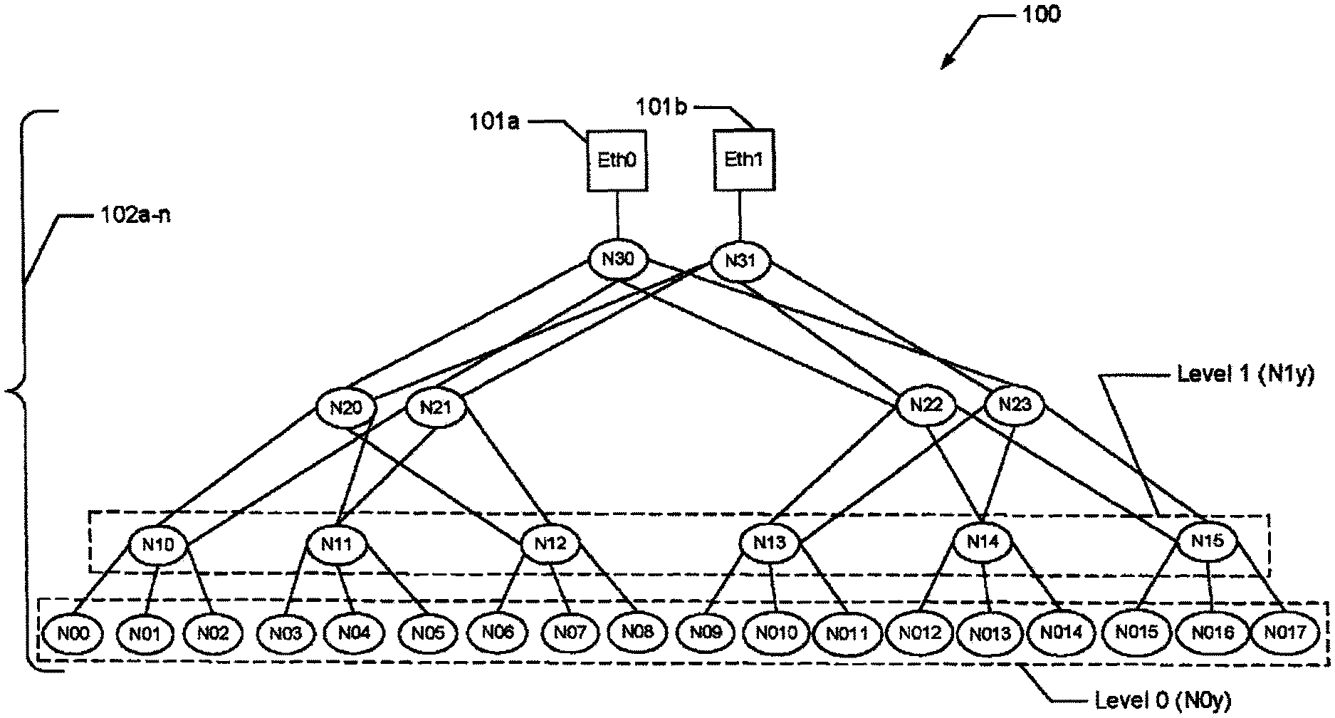
FIG. 1 is a high level diagram of a topology for a network system;
FIG. 2 is a block diagram of a network node in accordance with one embodiment of the present invention;
FIG. 3 is a block diagram of a network node in accordance with a second embodiment of the present invention;
FIG. 4 is a diagram showing local to remote address mapping;
FIG. 5 is a diagram showing validation of a remote transaction;
FIG. 6 is a schematic depicting an I/O physicalization; and
FIG. 7 is a schematic showing high performance distributed shared storage.
FIG. 8A is a diagram showing a node cluster architecture in accordance with one embodiment of the present invention.
FIG. 8B is a diagram showing a memory controller node chassis in accordance with one embodiment of the present invention.
FIG. 8C is a diagram showing a rack with a plurality of compute node chassis utilized in a rack with the memory controller node chassis of FIG. 8B in accordance with one embodiment of the present invention.
FIG. 9 is a diagram showing a memory hierarchy structure for computer nodes in accordance with one embodiment of the present invention.
FIG. 10 is a diagram showing a functional block diagram configured for implementing remote memory access functionality in accordance with one embodiment of the present invention.
FIG. 11 is a diagram showing physical address space of a particular one of the compute nodes shown in FIG. 8.
FIG. 12 is a diagram showing an embodiment of the present invention configured for providing memcached server functionality.
FIG. 13A is a diagram showing an embodiment of the present invention configured for implementing memory storage functionality using Partitioned Global Address Space (PGAS) languages.
FIG. 13B is a diagram showing a global memory space that is partitioned between participating threads for pooled memory functionality using PGAS languages.
FIG. 14A is a diagram showing an embodiment of the present invention configured for implementing hybrid memory cube (HMC) deployed near memory pools.
FIG. 14B is a diagram showing a private HMC of compute nodes coupled to a HMC deployed near memory pool.
FIG. 15 illustrates a logical view of a system on a chip (SoC).
FIG. 16 illustrates a software view of a power management unit.
DETAILED DESCRIPTION
FIG. 1 shows an example of a high-level topology of a network system 100 that illustrates compute nodes connected by a switched interconnect fabric. Network ports 101a and 101b come from the top of the fabric to external network connectivity. These network ports are typically Ethernet, but other types of networking including Infiniband are possible. Hybrid nodes 102a-n are compute nodes that comprise both computational processors as well as a fabric packet switch. The hybrid nodes 102a-n have multiple interconnect links to comprise the distributed fabric interconnect (i.e., a node interconnect fabric that provides an inter-node communication channel between a plurality of SoC nodes).
A recommended implementation for the fabric interconnect is a high-speed SerDes interconnect, such as multi-lane XAUI. In the preferred solution, a four-lane XAUI interconnect is used. Each of the four lanes can also have the speed varied from 1 Gb/sec (SGMII), XAUI rate (3.125 Gb/sec), and double XAUI (6.25 Gb/sec). The actual number of lanes and variability of speeds of each lane are implementation specific, and not important to the described innovations. Other interconnect technologies can be used that have a means to adaptively change the effective bandwidth, by varying some combination of link speeds and widths. Power consumption of a link is usually related to the delivered bandwidth of the link. By reducing the delivered bandwidth of the link, either through link speed or width, the power consumption of the link can be reduced.
Related application Ser. No. 12/794,996 (incorporated by reference) describes the architecture of a power-optimized, high performance, scalable inter-processor communication fabric. FIG. 1 shows a high-level topology 100 of a network system, such as described in the '996 Related Application, that illustrates XAUI connected SoC nodes connected by the switching fabric. The 10 Gb Ethernet ports EthO 101a and Ethl 101b come from the top of the tree. Most, if not all of the hybrid nodes 102a-n comprise both computational processors as well as an embedded switch as described below in conjunction with FIGS. 2-3. The hybrid nodes 102a-n have five XAUI links connected to the internal switch. The switching layers use all five XAUI links for switching. For example, as shown in FIG. 1, level 0 leaf nodes 102d, e (i.e., NOn nodes, or Nxy, where x=level and y=item number) only use one XAUI link to attach to the interconnect, leaving four high-speed ports that can be used as XAUI, 10 Gb Ethernet, PCIe, SATA, etc., for attachment to I/O. The vast majority of trees and fat tree-type network systems have active nodes only as leaf nodes, and the other nodes are pure switching nodes. This approach makes routing much more straightforward. Network system 100 has the flexibility to permit every hybrid node 102a-n to be a combination computational and switch node, or just a switch node. Most tree-type implementations have I/O on the leaf nodes, but system 100 lets the I/O be on any node. In general, placing the Ethernet at the top of the tree as at 101a/101b minimizes the average number of hops to the Ethernet.
In a preferred example, the hybrid nodes 102a-n shown in the tree-oriented topology of system 100 in FIG. 1 may represent independent nodes within a computing cluster. FIG. 1 illustrates one example implementation of individual nodes 102a-n of the cluster. When looking at a conventional implementation of a topology e.g. in FIG. 1, computing nodes are usually found in the lower level leaf nodes (e.g. N00-N017), and the upper level nodes do not have computing elements but are just network switching elements (N20-N31).
FIG. 2 illustrates one example of a "personality module" 200 in accordance with the present invention which is specifically designed for Ethernet protocol. Such an Ethernet personality module 200 can be used as a hybrid node for one or more of the nodes 102a-n of FIG. 1. With the node architecture shown in FIG. 2, the CPU Cores 206 of each personality module may be optionally enabled, or could be just left powered-off. With a personality module 200 used for the upper level switching nodes (N20-N30) in FIG. 1, the modules can be operated as pure switching elements (like traditional implementations), or the CPU Cores module 206 can be enabled and used as complete compute nodes within the computing cluster.
Note that the tree oriented interconnect fabric of FIG. 1 is simply one example of a type of server interconnect fabric. The concepts and inventions described herein have no dependency on the specific topology of interconnect fabric or protocol employed.
In more detail, the personality module 200 of FIG. 2 may be used as one or more of the hybrid nodes in the network system of FIG. 1. In FIG. 2, processors 205/206 communicate with the Ethernet MAC controllers 202 via the internal SOC processor bus fabric 201. Ethernet MAC controllers 202 generate Ethernet frames. The Ethernet Bridges 203 prepend a fabric routing header to the beginning of the Ethernet Frame. The Ethernet Bridges 203 contains the layer 2 Ethernet processing and computes the routing header based upon a distributed layer 2 Ethernet switch. A skilled person will appreciate that processors utilized in embodiments of the present invention (e.g., processors 205/206) are not unnecessarily limited to any particular model or brand of processor.
The Ethernet Bridges 203 in FIG. 2 receives an Ethernet frame from the Ethernet MAC controllers 202 in FIG. 2, sending an augmented routing frame to the fabric switch 204. Note that all frames that are flowing within the fabric are routing frames, not Ethernet frames. The Ethernet frame/routing frame conversion is done only as the packet is entering or leaving the fabric via a MAC. Note also that the routing logic within the switch may change fields within the routing frame. The Ethernet frame is never modified (except the adding/removing of the preamble, start of frame, and inter-frame gap fields).
The routing frame is composed of several fields providing sufficient data for the fabric switch 204 of FIG. 2 to make routing and security decisions without inspection of the underlying Ethernet frame which is considered an opaque payload. The resulting routing frame is thus a catenation of the routing frame header and the payload frame.
Related application Ser. No. 12/794,996 (incorporated by reference) disclosed in more detail an Ethernet protocol focused fabric switch. In the related '996 application two primary components are described: An Ethernet Routing Header processor that inspects Ethernet frames, and adds/removes the fabric switch routing header. The fabric switch that is responsible for transporting the packet between nodes by only using data from the routing header.
A key attribute of the Fabric Switch, 204 in FIG. 2, is that packets may be securely routed to their destination node/port by only using data in the routing header, without any inspection of the underlying data payload. Thus the data payload is considered opaque and invariant.
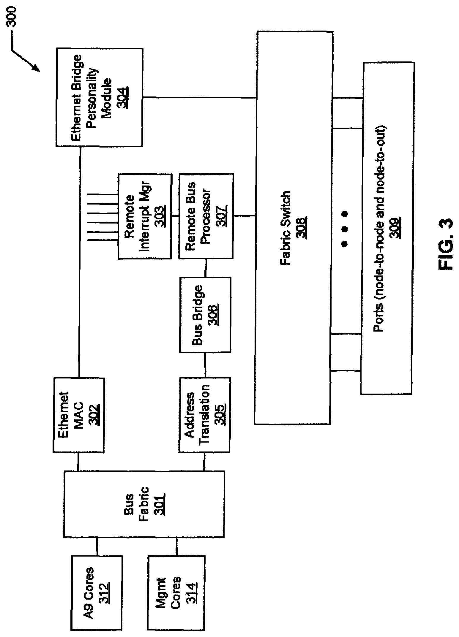
FIG. 3 illustrates a preferred embodiment of a multi-protocol personality module 300 that is similar to the Ethernet protocol module of FIG. 2. The module of FIG. 3 is similar to the Ethernet fabric module of FIG. 2 in that it continues to be responsible for transporting packets between nodes by only using data from the routing header. However, the multi-protocol personality module 300 of FIG. 3 operates with multiple protocols to accommodate a network operating with different protocols. Protocol specific personality modules are added such that routing header processing is done in new and separate fabric personality modules that provide mappings from specific protocol semantics to fabric routing headers. The multi-protocol personality module 300 of FIG. 3, like the Ethernet module of FIG. 2, is responsible for adding a routing header for packets entering the fabric, and removing the routing header when packets are leaving the fabric. The routing header maintains in place as the packets are transported node to node across the fabric.
The multi-protocol personality module 300 of FIG. 3 includes a portion for processing Ethernet (302, 304) which function much like the module of FIG. 2, and a portion (e.g., components 303, 305, 306, 307) for allowing bus transactions to be transported across the fabric, offering the ability to remote memory, I/O, and interrupt transactions across the fabric. In some embodiments of the present invention, a Remote Bus Personality Module of the multi-protocol personality module 300 comprises the portion of the multi-protocol personality module 300 that allows bus transactions to be transported across the fabric thereby enabling the ability to remote memory, I/O, and interrupt transactions across the fabric. In this regard, the Remote Bus Personality Module enables functionality related to allowing bus transactions to be transported across the fabric thereby provides the ability to remote memory, I/O, and interrupt transactions across the fabric.
As can be seen from the block diagram of FIG. 3 depicting an exemplary multi-protocol module 300, the Fabric Switch 308 transports packets across nodes of inter-node fabric (i.e., an inter-node communication channel defined thereby) therebetween by inspection of only the routing header. The routing header is composed of several fields providing sufficient data for the fabric switch 308 to make routing and security decisions without inspection of the underlying opaque data payload. The resulting routing frame is thus a catenation of the routing frame header and the opaque payload frame. One example of a payload frame is an Ethernet frame. For example, as shown in Table 1 below, a routing frame might comprise:
TABLE-US-00001 TABLE 1 Routing Frame Header Ethernet Frame Packet RF Header MAC MAC Ethertype/ Payload (data CRC32 destination Source Length and padding)
An example of a routing header follows in Table 2, but the fields may vary by implementation:
TABLE-US-00002 TABLE 2 Width Field (Bits) Notes Domain ID 5 Domain ID associated with this packet. 0 indicates that no domain has been specified. Mgmt Domain 1 Specifies that the packet is allowed on the private management domain. Source Node 12 Source node ID Source Port 2 0 = MAC0, 1 = MAC1, 2 = MAC_management processor, 3 = MAC OUT Dest Node 12 Destination node ID Dest Port 2 0 = MAC0, 1 = MAC1, 2 = MAC_management processor, 3 = MAC OUT RF Type 2 Routing Frame Type (0 = Unicast, 1 = Multicast, 2 = Neighbor Multicast, 3 = Link Directed) TTL 6 Time to Live - # of hops that this frame has existed. Switch will drop packet if the TTL threshold is exceeded (and notify management processor of exception). Broadcast ID 5 Broadcast ID for this source node for this broadcast packet. Checksum Checksum of the frame header fields.
Since the Fabric Switch 308 makes routing decisions by inspection of only the routing header, and the data payload frame is considered both opaque and invariant, these characteristics can be leveraged to create an extensible set of personality modules. A multi-protocol personality module 300 such as shown in FIG. 3 provides a mapping from specific protocols to add and remove the fabric routing headers for that protocol.
When using a personality module 300 such as shown in FIG. 3 as a hybrid node 102a-n in the system of FIG. 1, as previously stated, all frames that are flowing within the fabric are routing frames, not Ethernet frames. The payload frame/routing frame conversion is done only as the packet is entering or leaving the fabric. Note also that the routing logic within the switch may change fields within the routing frame. The payload frame is never modified.
The Ethernet Bridge personality processor 304 in FIG. 3, is functionally identical to the Routing Header processor in Related application Ser. No. 12/794,996, but generalized from a single-protocol processor (such as FIG. 2), to a module having a number of protocol processing portions. The Ethernet Bridge Processor 304 adds the routing header as the packet comes from the Ethernet MAC 302 to the fabric switch 308, and removes the routing header as the packet comes from the fabric switch 308 to the MAC 302.
Similar to FIG. 2, the processors 312/314 communicate with the Ethernet MAC controllers 302 in FIG. 3 via the internal SOC processor bus fabric 301. Ethernet MAC controllers 302 generate Ethernet frames. The Ethernet Bridge 304 prepends a fabric routing header to the beginning of the Ethernet Frame. The Ethernet Bridge 304 contains the layer 2 Ethernet processing and computes the routing header based upon a distributed layer 2 Ethernet switch.
As disclosed above in reference to the multi-protocol personality module 300 of FIG. 3, the Remote Bus Personality Module includes the Remote Interrupt Manager 303, the Remote Address translation module 305, the Bus Bridge 306 and the Remote Bus Processor 307. In FIG. 3, the Bus Fabric 301 represents the internal bus fabric of a system on a chip (SOC). As discussed below, the SoC can be configured to provide server functionality and thus be referred to as a server on a chip. This bus fabric carries CPU mastered load/store transactions to memory and I/O, as well as I/O mastered transactions, e.g. initiated by I/O DMA controllers.
The functionality of the Remote Bus personality Module consists of The Remote Address translation module 305, which converts local addresses steered to the Remote Bus Personality Module (RBPM) to [Remote Node, Remote Node Address]. The Bus Bridge 306, which converts a processor bus of arbitrary address and data width into a packed, potentially multi-flit packet. In this regard, the Bus Bridge 306 converts a processor bus of arbitrary address and data width into packetized transfers across the fabric. The Remote Bus Processor 307, which adds and removes the fabric routing header, transports bus packets from Bus Bridge 306 and interrupts from Remote Interrupt Manager 303 over the fabric in-order with guaranteed delivery.
The Remote Address translation module 305 converts local addresses steered to the RBFPM to [Remote Node, Remote Node Address]. This is depicted in more detail in FIG. 4 which shows that there is a set of mapping tables from [local address, size] to [Node ID, Remote address]. This address translation can be implemented as a custom module, typically leveraging a CAM (Content Addressable Memory). Alternatively, this stage may be implemented with a standard IP block of an I/O MMU (memory management unit) which translates the intermediate physical address in a bus transaction to a physical address. In this case, these translation tables are configured so that the resulting physical address encodes the [Remote Node ID, and Remote Address].
The Bus Bridge 306 of FIG. 3 functions to interface to and packetize the CPU/I/O bus transactions. In this regard, the Bus Bridge 306 can function as a packetizer. This Bus Bridge 306 is conceptually designed as having a layered model. In any given implementation, these layers may or may not be present, and will have tuned functionality for the bus bridging that is being implemented.
The multiple layer design of the Bus Bridge 306 is: Transaction layer The Transaction layer performs any necessary transforms that understand multiple bus channels or that understand the semantics of the transaction. Transfer layer (also known as Transport layer) The Transfer layer performs any necessary transforms within a channel related to the overall data transfer. This could include data compression. Data Link layer The Data Link layer performs arbitration, multiplexing and packing of channels to a physical packet representation. Implements any necessary flow control. Physical layer
The Physical layer performs transformation and optimization of the physical packet representation to packet size, width, and flit requirements to the fabric switch implementation. This Physical layer and/or the Link layer may actually produce multiple flits corresponding to a single physical bus packet.
The Remote Bus Processor 307 functions in a similar manner to the Ethernet Bridge Personality Processor 304 to add and remove the fabric routing header and transport bus packets from 306 to the fabric switch 308. Additionally, the Remote Bus Processor 307 connects interrupts from Remote Interrupt Manager 303 over the fabric with guaranteed delivery.
Example 1: Distributed One-Sided Cache Coherent Shared Memory Across the Fabric
In FIG. 1, one or more of the compute nodes could constitute servers, and the fabric connects two or more servers. The ability to open up memory sharing windows in another server across the fabric enables a wide-range of new capabilities that are not possible in traditional "shared nothing" clusters. In this example, the form that a load or store bus transaction issued by Server Node A is targeting a physical address in Server Node B. Such bus transactions may originate from any bus master in Node A, including processors, I/O bus masters (such as a SATA controller), or a DMA engine.
FIG. 4 illustrates the first stage of a remote shared memory access transaction using the Remote Bus Personality portion of the module of FIG. 3. As shown in FIG. 4, a bus master on Node A issues a load or store transaction to a range of physical addresses mapped to the Remote Bus Personality portion. The transaction appears as a bus transaction on FIG. 3, on Bus Fabric 301. The SOC busses of Bus Fabric 301, such as an ARM AXI, have configurable address and data widths, as an example 40 address bits, and 64-128 data bits.
The transaction flows through the Bus Bridge 306 as illustrated in FIG. 3 packetizing the bus transaction and creating one or more flits optimized for the fabric switch 308. The packetized transaction flows through the Remote Bus Processor 307 to create the routing header for the fabric. The remote bus packets are required to be delivered to destination server B in-order and with guaranteed delivery. If the underlying fabric and fabric switch do not implicitly have these characteristics, then the Remote Bus Processor 307 is required to implement in-order and guaranteed delivery.
The resulting routing frame flows into the fabric switch 308 on Node A, is routed through the intervening fabric (See FIG. 1), which may consists of multiple routing hops, and is delivered to the fabric switch on target Node B. For example, comparing FIG. 1, Node A might be node N30 and target Node B could be represented as node N014. The packet from fabric switch 308 of Node A is identified as a remote bus transaction, and is delivered to the Remote Bus Processor 307 on Node B.
Node B's Remote Bus Processor 307 implements the receiving side of in-order and guaranteed delivery in conjunction with the transmitting side. This can include notification of the sender of errors, missing flits, and request for retransmission, The Remote Bus Processor 307 of Node B then strips the routing header, sending the packetized transaction into the Bus Bridge 306. The Bus Bridge module 306 of Node B unpacks the packetized transaction (which may have included collecting multiple flits), and reconstitutes a valid transaction posted to Node B's bus. Any responses to that bus transaction are seen by this subsystem, and sent back to Node A following the same mechanism,
There are several functional and performance issues related to this cache coherency example. First, coherent memory transactions issued by CPUs in node A will not snoop caches on remote nodes to maintain efficiency. Second, incoming remote transactions from a Remote Bus Personality section can be implemented as one-sided cache coherent. This means that incoming loads or stores can optionally be configured to snoop and perform coherency protocols against processor caches. Finally, this provides a powerful, easy to use cache coherent programming mode without the performance and availability problems related to a full CC-NUMA (cache coherent--non-uniform memory access) design.
Example 2: Remote Bus Personality Module--Remote Interrupts
In many SOC bus infrastructures, interrupts are individual lines that feed into an interrupt controller for the processor(s) such as the Remote Interrupt Manager 303 of FIG. 3. These individual interrupt lines are sometimes OR'd with each other to map multiple interrupt sources to a single interrupt line.
For example, if server A (such as Node N30 of FIG. 1) processor generates an interrupt on server B (such as Node N14 of FIG. 1): First, Server A writes to a remote CSR (control status register) on server B which maps to the requested interrupt, such as the an interrupt line of Interrupt Manager 303 of FIG. 3. The interrupt line is made active and interrupts the Remote Bus Processor 307 on server B.
As another example, an I/O interrupt on server A can be reflected to an interrupt on server B. An I/O controller on server A (like a SATA controller) raises an interrupt line that is being monitored by the Remote Interrupt Manager 303, FIG. 3. The Remote Interrupt Manager 303 gets woken by an interrupt line that it is being monitored. Remote Interrupt Manager 303 creates a packet tagged as an interrupt packet and sends it into the Remote Bus Processor 307. This interrupt packet flows through the fabric as described above. When the interrupt packer reaches server B, the interrupt packet is delivered to Remote Bus Processor 307, which notes the specially tagged interrupt packet and sends it to the remote interrupt manager 303 of server B. Remote interrupt manager 303 causes the specified interrupt line to go active in server B.
Example 3: Remote Address Translation and Security
Referring to FIG. 3, block 314 is a management CPU core (See also Mgmt Core 205 of FIG. 2). This management CPU 314 is a key part of maintaining fabric security for remote bus transactions. The management CPU 314 maintains multi-node fabric transaction security on both sides of the transaction.
Each Remote Bus Processor 307 is allocated a range of addresses in physical address space. An exemplary process for the secure mapping of an address range from Server B into Server A's address space is as follows. 1. Main OS processor on Server A (block 312 in FIG. 3) sends a mapping request of tuple (node #, physical address in node #'s address space, and window length) to local management processor. 2. Management CPU 314 on Server A has the ability to accept or deny the remote mapping request. Upon local acceptance, management CPU on server A sends a secure management request with the remote mapping request to management CPU 314 on server B. 3. Management CPU 314 on server B has the ability to accept or deny the remote mapping request from Server A. 4. Upon acceptance, management CPU 314 on server B installs a mapping into the I/O MMU on server B, mapping an IPA window to the requested physical address. Additionally the Remote Bus Processor 307 on server B installs a mapping that designates that remote node A has access to that window. Mappings can be granted as read-only, write-only, or read-write. These mappings are illustrated in FIG. 5. These mappings can be implemented using a standard IP block like an I/O MMU, or with custom logic typically using a CAM. 5. Management CPU 314 on server B returns the base intermediate physical address of the window. 6. Management CPU 314 on server A installs a mapping into the local I/O MIVIU mapping from an IPA window on server A to the server B IPA window base address. 7 Management CPU 314 on server A returns the allocated local IPA address for the requested window to the requesting client on the main OS processor 312.
In the described examples, DMA engines on both the local (server A) and remote (server B) sides can be used to hardware facilitate data movement in either direction. Users are not constrained to the classic push OR pull data movement model. Further, many SOC bus transaction models have some notion of trust or security zone associated with that bus transaction. As an example, ARM AXI has the notion of TrustZone, where transactions are marked as being in Trusted World or Normal World. The Remote Bus portion in the Personality Module 300 illustrated in FIG. 3 annotates the bus transaction packet with the trust or security zone with the incoming bus transaction. When the remote server (e.g. server B) is issuing the remote transaction into the local bus fabric, a configuration option is used to define whether the transactions get issued with either the security zone of the requesting processor, or issued at a specific security zone level.
Example 4: Remote Bus Personality Module I/O Physicalization
FIG. 6 illustrates using the Remote Bus Personality portion of the Module 300 of FIG. 3 (i.e., the Remote Bus Personality Module) for I/O Physicalization. Some data center customers desire to have compute servers that have no embedded storage or I/O within the server, and then separate I/O boxes/chassis within the data center rack. The Remote Bus Personality Module of FIG. 3 allows multiple servers, designated as Srvr A, B, and C in FIG. 6, to use unmodified device drivers within the operating systems running in servers A, B, and C to access physically remote I/O devices across the server fabric. The server operating system, device drivers, and applications believe that they are communicating with server local devices. Use of the Remote Bus Personality Module of FIG. 3 allows the device I/O and interrupts to the actual I/O device to be bi-directionally remoted across the fabric with no changes or visibility to software.
Device drivers running on CPUs in the Server boxes (A, B, C) of FIG. 6 access I/O registers transparently across Fabric 608 in the remoted peripheral controller cards, illustrated as remote PCIe controllers 610/612 and remote SATA controllers 614/616 in FIG. 6. Direct memory access ("DMA") engines are located either in the server boxes, or alternatively in the I/O boxes embedded within the peripheral controllers, and the DMA traffic is remoted bi-directionally transparently across Fabric 608. Additionally, interrupts generated by the remote peripheral controllers are transparently transmitted across Fabric 608 and presented to the processors in servers A, B, or C. In this manner, the Remote Bus Personality Module enables remote memory access functionality which includes the ability to allow memory capacity to be provisioned based on workload on a per-node basis, to load/store from remote memory, to perform remote DMA transactions, and to perform remote interrupts.
The address maps, both I/O and memory, and interrupt maps are maintained and transmitted transparently across Fabric 608. In this example, the data flow is completely optimized. An example storage block transfer from SATA controller 614/616 of FIG. 6 would typically become: The device driver on Srvr B is reading a block from remote SATA 614 connected SSD 620 to a pre-allocated block buffer on a physical address PA1. The device driver programs and initiates the read by writing the appropriate control registers in remote SATA controller 614. Remote SATA controller 614 contains an embedded DMA engine which initiates the DMA, reading the data from the remoted SSD, and landing the data directly into physical address PA1 in Srvr B's address space. No network communication or additional data copies were needed in this optimized transfer.
Example 5: Remote Bus Personality Module Enabling High Performance Distributed Shared Storage
FIG. 7 illustrates an alternate distributed storage example. Distributed storage functionality is an embodiment of remote memory access functionality in which the remote memory is non-volatile memory (i.e., storage type memory), In this case the computational servers are illustrated as Srvr A, B, C. The I/O server boxes containing the storage peripherals in this use case have processors as well. This high performance shared storage example has one additional data movement from the example 4, I/O physicalization. But this example 5 adds the additional capabilities that the I/O devices and controllers can be shared by multiple servers.
In FIG. 7 a method of storage block transfer from a SATA controller is as follows. The device driver on Srvr A is reading a block from remote SATA 714 connected SSD 716 to a pre-allocated block buffer on a physical address PA1. The read is initiated by sending a lightweight message across Fabric 708 from Srvr A to Target I/O server 720 that contains the description of the read (device, block, size) and the physical address in Srvr A that the data should be moved to. The driver on SATA device 714 on Target I/O server 720 initiates the DMA read to its local buffer from its local SATA controller. Upon the completion of the DMA transfer to the I/O servers buffer, the device driver on the I/O server 720 uses a local DMA engine to initiate a fabric remoted DMA transfer from its local buffer to the physical address of the buffer in the requesting server's address space. The device driver programs and initiates the read by writing the appropriate control registers in controller of remote SATA 714.
This example requires one additional data movement as compared to the I/O Physicalization example 4, but is far more efficient than a traditional network oriented SAN or NAS remote storage data movement.
The discussion now turns to disassociation of memory (e.g., preferably mutable memory) from a cluster of nodes while enabling those nodes the ability to do full load/store/barrier instructions to a memory pool (e.g., aggregation of memory resources provided at a centralized location) through allocation of memory of the memory pool to the nodes based on workload on a per-node basis. Such implementation is referred to herein as pooled memory functionality. Implementing pooled memory functionality in this manner supports allocation of memory privately on a per node basis and allocation of memory to all or a portion of the nodes in a non-coherent, shared manner. Furthermore, in view of the disclosures made herein, a skilled person will appreciate that remote memory access functionality in accordance with the present invention supports implementation of near shared memory using, for example, HMC (hybrid memory cubes) memory resources and supports implementation of far shared memory over a SoC node fabric using, for example, both HMC and DDR memory resources.
A node cluster architecture 800 is shown in FIG. 8A. The node cluster architecture 800 is configured for providing remote memory access functionality in accordance with the present invention. More specifically, the node cluster architecture 800 includes a plurality of compute nodes 805 and a plurality of memory controller nodes 810 that are connected via a fabric 815 (i.e., links extending between fabric switches of interconnected nodes). Each one of the memory controller nodes 810 has memory 820 coupled thereto. Jointly, the memory 820 attached to all or a portion of the memory control nodes 810 is referred to herein as pooled memory. Preferably, aside from resident memory provisioning, the underlying architecture of the compute nodes 805 and the memory controller nodes 810 is entirely or substantially the same.
A plurality of the compute nodes 805 can be provided on a single card (i.e., a compute node card) and a plurality of the memory controller nodes 810 can be provided on a single card (i.e., a memory controller node card). The compute node card and memory controller node card can have identical overall planar dimensions such that both types of cards have a common or identical planar form factor. Each compute node 805 and each memory controller node 810 can have a plurality of SoC units thereon that provide information processing functionality. By definition, a compute node card will be populated more densely with SoC units that will be a memory controller node card. Preferably, but not necessarily, an architecture of the SoC units of the compute node cards is substantially the same or identical to that of the memory controller node cards,
The compute nodes 805 are each provisioned (i.e., configured) with a limited amount of local memory 807 and are packaged together (i.e., integrated with each other) with the goal of optimizing compute density within a given form factor (i.e., maximizing computer density in regard to cost, performance, space, heat generation, power consumption and the like). The memory controller nodes 810 are provisioned with a relatively large amount of local memory and together provide the pooled memory resource at a chassis, rack or cluster level (i.e., to maximizing poled memory in regard to cost, performance, space, heat generation, power consumption and the like for a given form factor). Put differently, a compute node card has insufficient memory resources for enabling intended data computing performance (e.g., data processing throughput) of compute nodes thereof and a memory controller node card has insufficient node CPU resources for enabling intended data computing performance (e.g., put/get and/or load/store utilization) of the pooled memory thereof. In this regard, intended data computing functionality of the server apparatus requires that the server apparatus include at least one computer node card and at least one memory controller card
Each compute node 805 can be allocated a portion of the pooled memory 820, which then serves as allocated memory to that particular one of the compute nodes 805. In this regard, the pooled memory 820 can be selectively allocated to and be selectively accessed by each one of the nodes (i.e., via pooled memory functionality). As shown in FIG. 8B, the one or more memory controller nodes 810 and associated pooled memory 820 (e.g., DDR as shown or HMC) can be implemented in the form of a memory controller node chassis 821. As shown in FIG. 8C, the memory controller node chassis 821 can be utilized in a rack 822 with a plurality of compute node chassis 823 that share memory resources of the memory controller node chassis 821. In this regard, one or more compute nodes 805 (or cards comprising same) and one or more memory controller nodes 810 with associated pooled memory 820 (or cards comprising same) can be referred to as a pooled memory server apparatus. It is also disclosed herein that a pooled memory server apparatus configured in accordance with the present invention can include a storage controller node chassis that is similar to the memory controller chassis except with storage resources (e.g., non-volatile storage resources such as hard disk drives) as opposed to memory resources (e.g., RAM).
In view of the disclosures made herein, a skilled person will appreciate that an underlying goal of the node cluster architecture 800 is to provide a fabric attached pool of memory (i.e., pooled memory) that can be flexibly assigned to compute nodes. For example, in the case of a dense node board such as that offered by Calxeda Inc under the trademark EnergyCard, every node of the compute node card (i.e., a plurality of nodes on a single board substrate) has a constrained, small number of DIMMs (e.g., every compute node having a constrained, small no. of DIMMs (e.g., 1)) and requires every node to have a relatively constrained amount of DRAM (e.g., every compute node to have something 4-8 GB of DRAM). But, in practical system implementations, some nodes will need different memory provisioning for specific requirements thereof (e.g., for Hadoop NameNode functionality, for Memcache functionality, for database functionality).
Pooled memory in accordance with embodiments of the present invention, which is attached to computer nodes though a fabric (i.e., fabric memory pools), support standardized dense node cards such as the Calxeda brand EnergyCard but allows them to be memory provisioned differently. In one specific implementation (shown in FIG. 8A), the bulk of the node cards in a cluster are cards with compute nodes (i.e., compute node cards). These compute node cards are configured with memory that is optimized with respect to capacity, power, and cost (e.g., one DIMM per channel). A variant of the compute node cards are cards are configured with associated pooled memory (i.e., pooled memory cards). The pooled memory cards, which are memory controller node cards in combination with associated pooled memory thereon, can be configured as maximum DRAM capacity cards. For example, the pooled memory cards can utilize multiple DIMMs per channel, RDIMMs at high densities (and higher power) or the like. This additional DRAM power is amortized across the fabric because there are likely a relatively small number of these pooled memory cards in comparison to compute node cards.
Embodiments of the present invention allow for pooled memory cards to be physically provisioned in a variety of different configurations. In support of these various physical provisioning configurations, pooled memory cards can be provisioned based on DIMM density (e.g., maximized DIMM density) or can be provisioned based on DRAM capacity (e.g., maximized DRAM capacity). In regard physical placement of the pooled memory cards, various rack and chassis positioned are envisioned. In one implementation (i.e., chassis provisioning), all or a portion of the pooled memory cards are configured for maximum DRAM capacity and serve as a chassis fabric memory pool. In another implementation (i.e., rack provisioning), a memory appliance (1U or 2U) is fabric connected within the rack using pooled memory cards are configured for maximum DRAM capacity. In another implementation (i.e., end of row provisioning), an entire rack is provided with pooled memory cards and serves as a memory rack that is at the end of a row of racks with computer nodes (i.e., compute racks). In still another implementation (i.e., distributed provisioning), all pooled memory cards are configured for maximum DRAM capacity and Linux NUMA APIs are used to create a distributed far memory pool. Additionally, Linux can even round-robin pages across the NUMA memory pool.
FIG. 9 shows a memory hierarchy structure 900 of each one of the computer nodes 805. As shown, the memory hierarchy structure 900 of each one of the computer nodes 805 has various memory resources. Of particular interest to remote memory access functionality implemented in accordance with the present invention is Remote Memory Layer 905, which introduces an additional level into the memory hierarchy structure 900 of each compute node. The Remote Memory Layer 905 enables a SoC (i.e., system) architecture where memory resources can be pooled at the cluster level and allocated amongst the nodes in a cluster (i.e., a plurality of nodes interconnected by a fabric). The Remote Memory Layer 905 allows memory capacity per node to be changed based on workload needs by changing the amount of pooled memory that is provisioned per node. This disaggregation and pooling of memory resources at the cluster level provides for better overall memory capacity utilization and lower power. Furthermore, the Remote Memory Layer 905 supports two types of accesses to remote memory that is mapped into a node's physical address space: a) coarse-grain accesses that rely in virtual-memory paging and involves transferring pages between remote and local memories and, b) fine-grain accesses that trigger cacheline transfers from the remote memory as a result of loads/stores from a node's operating system CPU to remote memory.
FIG. 10 shows a functional block diagram 1000 configured for implementing remote memory access functionality. The functional block diagram 1000 supports remote memory by a compute node 1005 (i.e., one of a plurality of computer nodes) across a fabric 1010. A Messaging Personality Module (i.e., the Messaging PM 1015) of the compute node 1005 serves as a hardware interface to remote DRAM 1020 (i.e., remote memory). The Messaging PM 1015 is connected to a cache coherent interconnect 1025 of the computer node 1005 such as through AXI Master and Slave interfaces thereof. The cache coherent interconnect 1025 has direct access to internal SRAM 1026 of the computer node 1005. Local DRAM 1127 (e.g., on a card level substrate on which the node is mounted) is coupled to the cache coherent interconnect 1025 via one or more memory controllers 129. Remote memory addresses of the remote DRAM 1020 are mapped to the Messaging PM 1005 through the AXI Master Port on the cache coherent interface 1025. Loads and stores to the remote DRAM 1020 by management cores 1030 (i.e., management processors) and operating system cores 1035 (i.e., OS processors) are diverted to the Messaging PM 1015, which then encapsulates these accesses in fabric packets and transports them to a memory controller node 1040 that serves the remote DRAM 1020 (i.e., the receiving controller node 1140). The memory controller node 1040 that serves the remote DRAM 1020 includes an instance of the Messaging PM. The receiving Messaging PM 1040 performs the requested access by reading or writing the local memory (e.g., local DRAM) of the memory controller node through its cache coherent interconnect.
In one embodiment, the functional block diagram 1000 is implemented via components of the multi-protocol personality module 300 discussed above in reference to FIG. 3. The Messaging PM 1005 can be embodied by the Remote interrupt Manager 303, the Remote Address translation module 305, the Bus Bridge 306 and the Remote Bus Processor 307. The cache coherent interconnect 1025 can be embodied by the bus fabric 301. The fabric 1010 can be implemented via one or more ports accessible to the fabric switch 308 for enabling access to the remote DRAM 1020.
In some embodiments of the present invention, the allocation of pooled memory (i.e., memory associated with one or more memory controller nodes) to individual compute nodes can managed by a cluster-level memory manager. This memory manager can be a software entity that is a standalone management entity or that is tightly integrated into other cluster-level management entities such as, for example, a job scheduler, a power management entity, etc. The allocation of the remote memory that is mapped into address space of a compute node to applications running on that computer node can be managed by an operating system (OS) or a virtual memory manager (VMM) using known virtual memory management and memory allocation techniques. For example, the OS and/or VMM can employ non-uniform memory access (NUMA) memory allocation techniques to distinguish between allocation of local memory and remote memory.
In view of the disclosures made herein, a skilled person will recognize that embodiments of the present invention enable various mechanisms of pooled memory functionality to be implemented. Pooled memory functionality is a specific implementation of remote memory access functionality. Examples of these mechanisms of pooled memory functionality include, but are not limited to, remote memory being mapped to physical address space of a node, load/store access being carried out from a CPU of a node, get/put access from user space, and DMA memory content transactions from remote memory to local memory. The benefits of these mechanisms of pooled memory functionality include, but are not limited to, disaggregated memory that can be used across multiple SoC generations, computer nodes can be assigned total memory based on workload characteristics, get/put into remote memory enables low-latency optimizations (e.g., via key/value stores, memcached, etc).
The remote memory architecture embodied within the functional block diagram 1000 can support two primary styles of pooled memory functionality. A first one of these styles of pooled memory functionality relates to shared remote memory. A second one of these styles of pooled memory functionality relates to disaggregated private memory. These use cases differ in whether an allocated portion of the pooled memory (i.e., remote memory) is mapped into the address space of a compute node and in how the allocated portion of the pooled memory is accessed.
The style of pooled memory functionality relating to shared remote memory involves remote memory get/put operations. In this style of pooled memory functionality, processor initiated bus cycles (i.e. load/stores) would not be directly remoted across the fabric. Rather, very low-latency user-space proxies for direct load/stores would be provided. These remote memory accesses represent get/put and/or load/store operations.
In the case pooled memory functionality relating to disaggregated private memory, as shown in FIG. 11, a physical address space 1105 of a particular compute node (e.g., a particular one of the compute nodes 805 shown in FIG. 8A) has local physical memory 1110 residing at its bottom portion and has the allocated remote memory (i.e., allocated remote memory 1115) mapped into its higher physical addresses. The allocated remote memory is not shared with any other nodes but is cacheable by management and OS cores of the node. Furthermore, the allocated remote memory is not directly accessible by user-space applications. In other words, accesses to allocated remote memory use physical addresses generated either by the paging mechanism implemented by the OS/VMM or by a memory management unit of the node's central processing unit. Accesses to allocated remote memory will typically higher latencies compared to accesses to local memory. This is due at least in part to memory bandwidth of the allocated remote memory being constrained by bi-section bandwidth of the fabric interconnecting the computer nodes and will likely be lower than the memory bandwidth of the local memory. Therefore, well-known memory hierarchy concepts such as caching and pre-fetching can be utilized for optimizing accesses to the allocated remote memory.
A primary goal of disaggregated private memory is to provide a fabric attached pool of memory (i.e., fabric attached pooled memory) that can be flexibly assigned to compute nodes. Native load/store transactions supported over a fabric. Examples of these native load/store transactions include, but are not limited to, transactions associated with global fabric address space, transactions associated with compute nodes carrying out read/write operations to remote memory, and transactions associated with remote DMA of memory content into physical memory of a compute node. In implementing disaggregated private memory in accordance with embodiments of the present invention, compute nodes will have private memory (e.g., private mutable memory) and can share a pool of fabric accessible memory (e.g., cacheable, non-coherent shared memory). Furthermore, fabric pool memory configured in accordance with embodiments of the present invention can be implemented within a chassis or across a largest possible fabric (e.g., across one or more rack).
Implementations of disaggregated private memory as disclosed herein can be considered as a class of remote NUMA memory (i.e., one-sided cache coherent which is also known as I/O coherent). For example, certain commercially available operating systems (e.g., Linux brand operating systems) have support for NUMA memory in the form of a NUMA subsystem, More specifically, Linux brand operating systems have NUMA awareness such as via numactl (e.g., control NUMA policy for processes or shared memory), Lib numa (e.g., NUMA policy API), and enhanced topology detection. Additionally, malloc-type memory allocation functionality is configured to ensure that the regions of memory that are allocated to a process are as physically close as possible to the core on which the process is executing, which increases memory access speeds. A node cluster architecture configured in accordance with the present invention can be configured to integrate with such a NUMA subsystem for allowing kernel and applications to have control of memory locality without having to expose new APIs and malloc-type memory allocation functionality for increasing memory access speeds.
Implementations of disaggregated private memory as disclosed herein can utilize device controllers (e.g., memory device controllers) that are physically allocated to remote nodes. This type of implementation is exemplified herein in the discussion relating to Example 4 and FIG. 6. Utilizing device controllers that are physically allocated to remote nodes allows the centralization of memory controllers and memory devices on a set of nodes. For example, the memory controllers and memory devices can be allocated to remote nodes at run-time whereby drivers continue to run on nodes acting as servers, drivers directly access remote memory controllers (e.g., of memory controller nodes), and DMA/interrupts are implemented transparent over the fabric that interconnects the nodes.
Example 6: Memcached Server Revolution
FIG. 12 illustrates an embodiment of the present invention configured for providing memcached server functionality 1200. The memcached server functionality 1200 utilizes pooled memory disclosed herein in accordance with the present invention. Memcached server functionality in accordance with the present invention is applicable to a large class of key-value store storage. Advantageously, implementation of the memcached server functionality 1200 in accordance with the present invention allows memcached clients 1205A, 1205B (e.g. web servers) to reach back to a pooled memory 1210 (i.e., memcached memory pool) to get cached values of data without having to go back to their respective database tier. For example, the pooled memory 1210 can be implemented as NUMA fabric pooled memory. The memcached clients 1205A, 1205B can be embodied by one or more compute nodes that are each allocated respective private mutable private memory 1215A, 1215B from pooled memory associated with one or more memory controller nodes. To this end, the memcached clients 1205, the pooled memory 1210, and the private mutable private memory 1215 can be embodied by the pooled memory server apparatus discussed above in reference to FIGS. 8a-8c.
The memcached clients 1205A, 1205B each map access information (e.g., a key) directly and reach into the pooled memory 1210 to obtain the data with a direct memory load. In this manner, unlike the traditional memcached approach, there is no networking needed for access memcached data. Each one of the memcached servers 1210a-e hashes into local DRAM and returns the hashed value over TCP/IP or UDP, which serves as the communication protocol between the memcached servers and each one of the memcached clients 1205.
In regard to a specific example in which a cluster of SoC nodes (i.e., including Node A and Node B) that are interconnected by a node interconnect fabric, Node A (e.g., through web server functionality thereof) requests an account lookup for Account #100. Web server request goes through a Memcached client API into a memcached client library with a cache data request for Key ID #100. The memcached client library hashes Key ID #100 to the memcached server that holds that data whereby it hashes to Node B that is providing memcached server functionality. The memcached client library determines that Node A and Node B have a remote memory capable fabric between them (e.g., are configured for providing remote memory access functionality in accordance with the present invention). The memcached client library on Node A performs a server-side hash of Key ID #100 and uses a remote memory access to node B to determine if this data is currently encached and, if so, the memory address that contains the data. In the case where it is determined that the data is currently encached, the memcached client library on Node A directly access the remote cached data from Node B's memory address space (e.g., memory address space of Node B's memcached server functionality). The memcached client library then returns the data to the requesting web server on Node A.
Example 7: High Frequency Trading Backend
In support of high frequency trading, stock exchange tick data can stream as multicast packets at rates up to 6 MB/sec or more. The tick data can be highly augmented with derived data thereof A fabric memory pool apparatus is used to store the tick data in one place and accessed by a plurality of trading servers. Referring to the pooled memory server apparatus discussed above in reference to FIGS. 8a-8c, the fabric memory pool apparatus can be embodied in the form of the memory controller node chassis 821 and the trading servers can be embodied in the form of the compute node chassis 823, The tick data is only appended such that the tick data does not have to be multicast and replicated. Furthermore, all compute nodes of the trading servers get direct read-only shared access to the tick data (i.e., via pooled memory of the memory controller nodes) whereby the tick data is still CPU cacheable for frequently accessed data.
Example 8: Message Passing Interface Remote Memory Access (One Sided)
The underlying premise of message passing interface (MPI) remote memory access (RMA) relates to any allocated memory is private to the MPI process by default. As needed, this allocated private memory can be exposed to other processes as a public memory region. To do this, an MPI process declares a segment of its memory to be part of a window, allowing other processes to access this memory segment using one-sided operations such as PUT, GET, ACCUMULATE, and others, Processes can control the visibility of data written using one-sided operations for other processes to access using several synchronization primitives. Referring to the pooled memory server apparatus discussed above in reference to FIGS. 8a-8c, memory of the MPI process can be embodied in the form of the memory controller node chassis 821.
MPI 3rd generation (i.e., MPI-3) RMA offers two new window allocation functions. The first new window allocation function is a collective version that can be used to allocate window memory for fast access. The second new window allocation function is a dynamic version which exposes no memory but allows the user to "register" remotely-accessible memory locally and dynamically at each process. Furthermore, new atomic operations, such as fetch-and-accumulate and compare-and-swap offer new functions for well-known shared memory semantics and enable the implementation of lock-free algorithms in distributed memory.
Example 9: Partitioned Global Address Space Languages (PGAS)
Examples of common PGAS languages include, but are not limited to, Unified Parallel C, Co-Array Fortran, Titanium, X-10, and Chapel. As shown in FIG. 13A, in these PGAS languages, memory distributed over many compute nodes (i.e., distributed memory 1300) is seen as one global memory (i.e., global memory 1305) that can be accessed by all the processes without requiring explicit communication like in MPI. Hidden communication is based on one-sided communication. As shown in FIG. 13B, PGAS languages introduce the concept of a global memory space 1310 that is partitioned between the participating threads 1315 (e.g., ranks in MPI) with each process being able to access both local memory (e.g., distributed memory 1300 local to a particular computer node) and remote memory (e.g., distributed memory 1300 local to a different computer node than the particular computer node). Access to local memory is via standard sequential program mechanisms whereas access to remote memory is directly supported by the new features of the PGAS language and is usually done in a "single-sided" manner (unlike the double-sided of MPI). The single-sided programming model is more natural than the MPI alternative for some algorithms. In accordance with embodiments of the present invention, RDMA and remote memory functionalities allow efficient PGAS capability to be provided. Referring to the pooled memory server apparatus discussed above in reference to FIGS. 8a-8c, the global memory 1305 can be embodied in the form of the memory controller node chassis 821.
Example 10: Disaggregated Server Resources
Currently, disaggregation of server resources is limited to separating compute resources (e.g., CPU and RAM) from storage via separate chassis that are connected via an interface such as, for example, PCIe or SAS. However, data centers and other types of server operating entities will benefit from disaggregation of CPU resources, storage resources, and memory resources. This will allow server operating entities to replace/update CPU resources, storage resources, and memory resources (i.e., server resources) at their respective lifecycle timeframe without having to replace/update one server resource at the particular lifecycle timeframe of another server resource. Advantageously, embodiments of the present invention can provide for such disaggregation of CPU resources, storage resources, and memory resources. In particular, embodiments of the present invention provide for the disaggregation of RAM (i.e., memory resources) from compute node cards (i.e., CPU resources) so that CPU resources can be replaced/updated as new CPU resources (e.g., processors) are released whereas memory resources (e.g., RAM, non-volatile storage, etc) can remain in use as long as they are efficient and/or effectively functional. To this end, referring to the pooled memory server apparatus discussed above in reference to FIGS. 8a-8c, the memory resources can be embodied in the form of the memory controller node chassis 821 (i.e., a first physical enclosure unit), the CPU resources can be embodied in the form of the compute node chassis 823 (i.e., a second physical enclosure unit), and the storage resources can be embodied in the form of the storage controller node chassis (i.e., a third physical enclosure unit). Memory resources can be in the form of one or more HMCs.
Example 11: Hybrid Memory Cube (HMC) Deployed Near Memory Pool
As shown in FIG. 14A, pooled memory functionality in accordance with the present invention can be implemented in the form of HMC deployed near memory pools. In such an implementation, a HMC unit (i.e., pooled memory) is shared by a plurality of compute nodes 1410 (i.e., the shared HMC unit 1405). For example, the compute nodes 1410 can all be of a common compute node card such as the Calxeda brand EnergyCard. As shown, each one of the compute nodes 1410 can also have respective base memory 1415. In this manner, the compute nodes 1410 can have non-coherent, shared memory and, optionally, private mutable memory. Referring to the pooled memory server apparatus discussed above in reference to FIGS. 8a-8c, the HMC unit can be embodied in the form of the memory controller node chassis 821 and the compute nodes 1410. CPU resources can be embodied in the form of the compute node chassis 823 and the HMC unit 1405 can be embodied in the form of the memory controller chassis. As a skilled person will appreciate, the near memory pools implemented with HMC units do not require a fabric for data communication. As shown in FIG. 14B, each one of the compute nodes 1410 has a respective private HMC 1420. The private HMC 1420 and the shared HMC 1405 each provide HMC links for supporting communication of data therebetween (e.g., 16-lane HMC link with 40 GB/sec link capacity). For example, the HMC units can each include a cache coherent interconnect 1425 (e.g., a fabric bus) having two memory ports (e.g., 25 GB/sec link capacity each) each coupled to a respective HMC controller 1430 by a bridge 1435. In view of the disclosures made herein, a skilled person will appreciate the compute nodes 1410 can be SoC nodes that are interconnected to each other through a node interconnect fabric and that access to the memory resources of the HMC unit 1405 is made over a respective communication link of the HMC unit 1405 without traversing any communication channel of the node interconnect fabric.
Example 12: Far Memory Pool Using Pooled Memory Functionality
Pooled memory functionality in accordance with the present invention can be implemented in the form of far memory pools. In such an implementation, pooled memory is shared by a plurality of compute nodes such as those of a compute node chassis configured in accordance with the present invention. The shared memory can be in the form of cache coherent DDR or cache coherent HMC such as that of a memory controller chassis configured in accordance with the present invention. The shared memory is accessed via a fabric that interconnects the computer nodes. Preferably, but not necessarily, the compute nodes are all of a common compute node card such as the Calxeda brand EnergyCard. Each one of the compute nodes can also have respective base memory. In this manner, the compute nodes can have non-coherent, shared memory and, optionally, private mutable memory.
In summary, in view of the disclosures made herein, a skilled person will appreciate that a system on a chip (SOC) refers to integration of one or more processors, one or more memory controllers, and one or more I/O controllers onto a single silicone chip. Furthermore, in view of the disclosures made herein, the skilled person will also appreciate that a SOC configured in accordance with the present invention can be specifically implemented in a manner to provide functionalities definitive of a server. In such implementations, a SOC in accordance with the present invention can be referred to as a server on a chip, In view of the disclosures made herein, the skilled person will appreciate that a server on a chip configured in accordance with the present invention can include a server memory subsystem, a server I/O controllers, and a server node interconnect. In one specific embodiment, this server on a chip will include a multi-core CPU, one or more memory controllers that supports ECC, and one or more volume server I/O controllers that minimally includes Ethernet and SATA controllers. The server on a chip can be structured as a plurality of interconnected subsystems, including a CPU subsystem, a peripherals subsystem, a system interconnect subsystem, and a management subsystem.
An exemplary embodiment of a server on a chip that is configured in accordance with the present invention is the ECX-1000 Series server on a chip offered by Calxeda incorporated. The ECX-1000 Series server on a chip includes a SOC architecture that provides reduced power consumption and reduced space requirements. The ECX-1000 Series server on a chip is well suited for computing environments such as, for example, scalable analytics, webserving, media streaming, infrastructure, cloud computing and cloud storage. A node card configured in accordance with the present invention can include a node card substrate having a plurality of the ECX-1000 Series server on a chip instances (i.e., each a server on a chip unit) mounted on the node card substrate and connected to electrical circuitry of the node card substrate. An electrical connector of the node card enables communication of signals between the node card and one or more other instances of the node card.
The ECX-1000 Series server on a chip includes a CPU subsystem (i.e., a processor complex) that uses a plurality of ARM brand processing cores (e.g., four ARM Cortex brand processing cores), which offer the ability to seamlessly turn on-and-off up to several times per second. The CPU subsystem is implemented with server-class workloads in mind and comes with a ECC L2 cache to enhance performance and reduce energy consumption by reducing cache misses. Complementing the ARM brand processing cores is a host of high-performance server-class I/O controllers via standard interfaces such as SATA and PCI Express interfaces. Table 3 below shows technical specification for a specific example of the ECX-1000 Series server on a chip.
TABLE-US-00003 TABLE 3 Example of ECX-1000 Series server on a chip technical specification Processor Cores 1. Up to four ARM .RTM. Cortex .TM.-A9 cores @ 1.1 to 1.4 GHz 2. NEON .RTM. technology extensions for multimedia and SIMD processing 3. Integrated FPU for floating point acceleration 4. Calxeda brand TrustZone .RTM. technology for enhanced security 5. Individual power domains per core to minimize overall power consumption Cache 1. 32 KB LI instruction cache per core 2. 32 KB LI data cache per core 3. 4 MB shared L2 cache with ECC Fabric Switch 1. Integrated 80 Gb (8x8) crossbar switch with through-traffic support 2. Five (5) 10 Gb external channels, three (3) 10 Gb internal channels 3. Configurable topology capable of connecting up to 4096 nodes 4. Dynamic Link Speed Control from 1 Gb to 10 Gb to minimize power and maximize performance 5. Network Proxy Support to maintain network presence even with node powered off Management 1. Separate embedded processor dedicated for Engine systems management 2. Advanced power management with dynamic power capping 3. Dedicated Ethernet MAC for out-of-band communication 4. Supports IPMI 2.0 and DCMI management protocols 5. Remote console support via Serial-over-LAN (SoL) Integrated 1. 72-bit DDR controller with ECC support Memory 32-bit physical memory addressing Controller 3. Supports DDR3 (1.5 V) and DDR3L (1.35 V) at 800/1066/1333 MT/s 4. Single and dual rank support with mirroring PCI Express 1. Four (4) integrated Gen2 PCIe controllers 2. One (1) integrated Genl PCIe controller 3. Support for up to two (2) PCIe x8 lanes 4. Support for up to four (4) PCIe x1, x2, or x4 lanes Networking 1. Support 1 Gb and 10 Gb Ethernet Interfaces 2. Up to five (5) XAUI 10 Gb ports 3. Up to six (6) 1 Gb SGMII ports (multiplexed w/XAUI ports) 4. Three (3) 10 Gb Ethernet MACS supporting IEEE 802.1Q VLANs, IPv4/6 checksum processing, and TCP/UDP/ICMP checksum offload 5. Support for shared or private management LAN SATA 1. Support for up to five (5) SATA disks Controllers 2. Compliant with Serial ATA 2.0, AHCI Revision 1.3, and eSATA specifications 3. SATA 1.5 Gb/s and 3.0 Gb/s speeds supported SD/eMMC 1. Compliant with SD 3.0 Host and MMC 4.4 Controller (eMMC) specifications 2. Supports 1 and 4-bit SD modes and 1/4/8-bit MMC modes 3. Read/write rates up to 832 Mbps for MMC and up to 416 Mbps for SD System 1. Three (3) 12C interfaces Integration 2. Two (2) SPI (master) interface Features 3. Two (2) high-speed DART interfaces 4. 64 GPIO/Interrupt pins 5. JTAG debug port
FIG. 15 shows a SoC unit (i.e., SoC 2200) configured in accordance with an embodiment of the present invention. More specifically, the SoC 2200 is configured for implementing discovery functionalities as disclosed herein. The SoC 2200 can be utilized in standalone manner. Alternatively, the SoC 2200 can be utilized in combination with a plurality of other SoCs on a node card such as, for example, with each one of the SoCs being associated with a respective node of the node card.
The SoC 2200 includes a node CPU subsystem 2202, a peripheral subsystem 2204, a system interconnect subsystem 2206, and a management subsystem 2208. In this regard, a SoC configured in accordance with the present invention can be logically divided into several subsystems. Each one of the subsystems includes a plurality of operation components therein that enable a particular one of the subsystems to provide functionality thereof. Furthermore, each one of these subsystems is preferably managed as independent power domains.
The node CPU subsystem 2202 of SoC 2200 provides the core CPU functionality for the SoC, and runs the primary user operating system (e.g. Ubuntu Linux). The Node CPU subsystem 2202 comprises a node CPU 2210, a L2 cache 2214, a L2 cache controller 2216, memory controller 2217, and main memory 2219. The node CPU 2210 includes 4 processing cores 2222 that share the L2 cache 2214. Preferably, the processing cores 2222 are each an ARM Cortex A9 brand processing core with an associated media processing engine (e.g., Neon brand processing engine) and each one of the processing cores 2222 can have independent L1 instruction cache and L1 data cache. Alternatively, each one of the processing cores can be a different brand of core that functions in a similar or substantially the same manner as ARM Cortex A9 brand processing core. Each one of the processing cores 2222 and its respective L1 cache is in a separate power domain. Optionally, the media processing engine of each processing core 2222 can be in a separate power domain. Preferably, all of the processing cores 2222 within the node CPU subsystem 2202 run at the same speed or are stopped (e.g., idled, dormant or powered down).
The memory controller 2217 is coupled to the L2 cache 2214 and to a peripheral switch of the peripheral subsystem 2204. Preferably, the memory controller 2217 is configured to control a plurality of different types of main memory (e.g., DDR3, DDR3L, LPDDR2). An internal interface of the memory controller 2217 can include a core data port, a peripherals data port, a data port of a power management unit (PMU) portion of the management subsystem 2208, and an asynchronous 32-bit AHB slave port. The PMU data port is desirable to ensure isolation for some low power states. The asynchronous 32-bit AHB slave port is used to configure the memory controller 2217 and access its registers. The asynchronous 32-bit AHB slave port is attached to the PMU fabric and can be synchronous to the PMU fabric in a similar manner as the asynchronous interface is at this end. In one implementation, the memory controller 2217 is an AXI interface (i.e., an Advanced eXtensible Interface).
The peripheral subsystem 2204 of SoC 2200 has the primary responsibility of providing interfaces that enable information storage and transfer functionality. This information storage and transfer functionality includes information storage and transfer both within a given SoC Node and with SoC Nodes accessibly by the given SoC Node. Examples of the information storage and transfer functionality include, but are not limited to, flash interface functionality, PCIe interface functionality, SATA interface functionality, and Ethernet interface functionality. The peripheral subsystem 2204 can also provide additional information storage and transfer functionality such as, for example, direct memory access (DMA) functionality. Each of these peripheral subsystem functionalities is provided by one or more respective controllers that interface to one or more corresponding storage media (i.e., storage media controllers).
The peripherals subsystem 2204 includes the peripheral switch and a plurality of peripheral controllers for providing the abovementioned information storage and transfer functionality. The peripheral switch can be implemented in the form of a High-Performance Matrix (HPM) that is a configurable auto-generated advanced microprocessor bus architecture 3 (i.e., AMBA protocol 3) bus subsystem based around a high-performance AXI cross-bar switch known as the AXI bus matrix, and extended by AMBA infrastructure components.
The peripherals subsystem 2204 includes flash controllers 2230 (i.e. a first type of peripheral controller). The flash controllers 2230 can provide support for any number of different flash memory configurations. A NAND flash controller such as that offered under the brand name Denali is an example of a suitable flash controller. Examples of flash media include MultiMediaCard (MMC) media, embedded MultiMediaCard (eMMC) media, Secure Digital (SD) media, SLC/MLC+ECC media, and the like. Memory is an example of media (i.e., storage media) and error correcting code (ECC) memory is an example of a type of memory to which the main memory 2217 interfaces (e.g., main memory 2219).
The peripherals subsystem 2204 includes Ethernet MAC controllers 2232 (i.e. a second type of peripheral controller). Each Ethernet MAC controller 2232 can be of the universal 1 Gig design configuration or the 10 G design configuration. The universal 1 Gig design configuration offers a preferred interface description. The Ethernet MAC controllers 2232 includes a control register set and a DMA (i.e., an AXI master and an AXI slave). Additionally, the peripherals subsystem 2204 can include an AXI2 Ethernet controller 2233. The peripherals subsystem 2204 includes a DMA controller 2234 (i.e., (i.e. a third type of peripheral controller). DMA functionality is useful only for fairly large transfers. Thus, because private memory of the management subsystem 2208 is relatively small, the assumption is that associated messages will be relatively small and can be handled by an interrupt process. If the management subsystem 2208 needs/wants large data transfer, it can power up the whole system except the cores and then DMA is available. The peripherals subsystem 2204 includes a SATA controller 2236 (i.e. a fourth type of peripheral controller). The peripherals subsystem 2204 also includes PCIe controllers 2238. As will be discussed below in greater detail, a XAUI controller of the peripherals subsystem 2204 is provided for enabling interfacing with other CPU nodes (e.g., of a common node card).
The system interconnect subsystem 2206 is a packet switch that provides intra-node and inter-node packet connectivity to Ethernet and within a cluster of nodes (e.g., small clusters up through integration with heterogeneous large enterprise data centers). The system interconnect subsystem 2206 provides a high-speed interconnect fabric, providing a dramatic increase in bandwidth and reduction in latency compared to traditional servers connected via 1 Gb Ethernet to a top of rack switch. Furthermore, the system interconnect subsystem 2206 is configured to provide adaptive link width and speed to optimize power based upon utilization.
An underlying objective of the system interconnect subsystem 2206 is support a scalable, power-optimized cluster fabric of server nodes. As such, the system interconnect subsystem 2206 has three primary functionalities. The first one of these functionalities is serving as a high-speed fabric upon which TCP/IP networking is built and upon which the operating system of the node CPU subsystem 2202 can provide transparent network access to associated network nodes and storage access to associated storage nodes. The second one of these functionalities is serving as a low-level messaging transport between associated nodes. The third one of these functionalities is serving as a transport for remote DMA between associated nodes.
The system interconnect subsystem 2206 can be connected to the node CPU subsystem 2202 and the management subsystem 2208 through a bus fabric (i.e., Ethernet AXIs) of the system interconnect subsystem 2206. An Ethernet interface of the system interconnect subsystem 2206 can be connected to peripheral interfaces (e.g., interfaces 2230, 2232, 2234, 2238) of the peripheral subsystem 2204. A fabric switch (i.e., a switch-mux) can be coupled between the XAUI link ports of the system interconnect subsystem 2206 and one or more MAC's 2243 of the system interconnect subsystem 2206. The XAUI link ports and MACs (i.e., high-speed interconnect interfaces) enabling the node that comprises the SoC 2200 to be connected to associated nodes each having their own SoC (e.g., identically configured SoCs).
The processor cores 2222 (i.e., A9 cores) of the node CPU subsystem 2202 and management processor 2270 (i.e., M3) of the management subsystem 2208 can address MACs (e.g., MAC 2243) of the system interconnect subsystem 2206. In certain embodiments, the processor cores 2222 of the node CPU subsystem 2202 will utilize a first MAC and second MAC and the management processor 2270 of the management subsystem 2208 will utilize a third MAC. To this end, MACs of the system interconnect subsystem 2206 can be configured specifically for their respective application.
The management subsystem 2208 is coupled directly to the node CPU subsystem 2202 and directly to the to the system interconnect subsystem 2206. An inter-processor communication (IPC) module (i.e., IPCM) of the management subsystem 2208, which includes IPC 2216, is coupled to the node CPU subsystem 2202, thereby directly coupling the management subsystem 2208 to the node CPU subsystem 2202. The management processor 2270 of the management subsystem 2208 is preferably, but not necessarily, an ARM Cortex brand M3 microprocessor. The management processor 2270 can have private ROM and private SRAM. The management processor 2270 can be coupled to shared peripherals and private peripherals of the management subsystem 2208. The private peripherals are only accessible by the management processor, whereas the shared peripherals are accessible by the management processor 2270 and each of the processing cores 2222. Instructions for implementing embodiments of the present invention (e.g., functionalities, processes and/or operations associated with r4emote memory access, pooled memory access, memcache, distributed memory, server resource disaggregation, and the like) can reside in non-transitory memory coupled to/allocated to the management processor 2270.
Additional capabilities arise because the management processor 2270 has visibility into all buses, peripherals, and controllers. It can directly access registers for statistics on all buses, memory controllers, network traffic, fabric links, and errors on all devices without disturbing or even the knowledge of the access by the core processing cores 2222. This allows for billing use cases where statistics can be gathered securely by the management processor without having to consume core processing resources (e.g., the processing cores 2222) to gather, and in a manner that cannot be altered by the core processor 2222.
The management processor 2270 has a plurality of responsibilities within its respective node. One responsibility of the management processor 2270 is booting an operating system of the node CPU 2210. Another responsibility of the management processor 2270 is node power management. Accordingly, the management subsystem 2208 can also be considered to comprise a power management Unit (PMU) for the node and thus, is sometime referred to as such. As discussed below in greater detail, the management subsystem 2208 controls power states to various power domains of the SoC 2200 (e.g., to the processing cores 2222 by regulating clocks). The management subsystem 2208 is an "always-on" power domain. However, the management processor 2270 can turn off the clocks to the management processor 2270 and/or its private and/or shared peripherals to reduce the dynamic power. Another responsibility of the management processor 2270 is varying synchronized clocks of the node CPU subsystem 2202 (e.g., of the node CPU 2210 and a snoop control unit (SCU)). Another responsibility of the management processor 2270 is providing baseboard management control (BMC) and IPMI functionalities including console virtualization. Another responsibility of the management processor 2270 is providing router management. Another responsibility of the management processor 2270 is acting as proxy for the processing cores 2222 for interrupts and/or for network traffic. For example, a generalized interrupt controller (GIC) of the node CPU subsystem 2202 will cause interrupts intended to be received by a particular one of the processing core 2222 to be reflected to the management processor 2270 for allowing the management processor 2270 to wake the particular one of the processing cores 2222 when an interrupt needs to be processed by the particular one of the of the processing cores that is sleeping, as will be discussed below in greater detail. Another responsibility of the management processor 2270 is controlling phased lock loops (PLLs). A frequency is set in the PLL and it is monitored for lock. Once lock is achieved the output is enabled to the clock control unit (CCU). The CCU is then signaled to enable the function. The management processor 2270 is also responsible for selecting the dividers but the actual change over will happen in a single cycle in hardware. Another responsibility of the management processor 2270 is controlling a configuration of a variable internal supply used to supply electrical power to the node CPU subsystem 2202. For example, a plurality of discrete power supplies (e.g., some being of different power supplying specification than others (e.g., some having different power capacity levels)) can be selectively activated and deactivated as necessary for meeting power requirements of the node CPU subsystem 2202 (e.g., based on power demands of the processing cores 2222, the SCU, and/or the controller of the L2 cache 2214). A separate power control mechanism (e.g., switch) can be used to control power supply to each of the processing cores 2222 and separately to the SCU. Another responsibility of the management processor 2270 is managing a real-time-clock (RTC) that exists on a shared peripheral bus of the management subsystem 2208. Another responsibility of the management processor 2270 is managing a watchdog timer on a private peripheral bus of the management subsystem 2208 to aid in recovery from catastrophic software failures. Still another responsibility of the management processor 2270 is managing an off-board EEPROM. The off-board EEPROM is device is used to store all or a portion of boot and node configuration information as well as all or a portion of IPMI statistics that require non-volatile storage. Each of these responsibilities of the management processor 2270 is an operational functionality managed by the management processor 2270. Accordingly, operational management functionality of each one of the subsystem refers to two or more of these responsibilities being managed by the management processor 2270.
As shown in FIG. 16, software 3300 is provided on the management processor 2270. The management processor 2270 includes a plurality of application tasks 3302, an operating system (OS)/input-output (I/O) abstraction layer 3304, a real-time operating system (RTOS) 3306, and device drivers 3308 for the various devices. The operating system (OS)/input-output (I/O) abstraction layer 3304 is a software layer that resides between the application tasks3 302 and the real-time operating system (RTOS) 3306. The operating system (OS)/input-output (I/O) abstraction layer 3304 aids in porting acquired software into this environment. The OS abstraction portion of the operating system (OS)/input-output (I/O) abstraction layer 3304 provides posix-like message queues, semaphores and mutexes. The device abstraction portion of the operating system (OS)/input-output (I/O) abstraction layer 3304 provides a device-transparent open/close/read/write interface much like the posix equivalent for those devices used by ported software. The real-time operating system (RTOS) 3306 resides between the operating system (OS)/input-output (I/O) abstraction layer 3304 and the device drivers 3308.
The application tasks 3302 include, but are not limited to, a boot task 3310, a system management task 3312, a power management task 3314, a serial concentrator task 3316, a frame switch management task 3318 (sometimes called routing management), and a network proxy task 3320. The boot task 3310 provides the function of booting the processing cores 2222 and the management processor 2270. The system management task3 312 provides the function of integrated operation of the various subsystems of the SOC 2200. The power management task 3314 provides the function of managing power utilization of the various subsystems of the SOC 2200. The serial concentrator task 3316 provides the function of managing communication from the other application tasks to a system console. This console may be directly connected to the SOC node via a DART (i.e., a universal asynchronous receiver/transmitter) or it can be connected to another node in the system. The frame switch management task 3318 (sometimes called routing management) is responsible for configuring and managing routing network functionality. As discussed in greater detail below, the network proxy task 3320 maintains network presence of one or more of the processing cores 2222 while in a low-power sleep/hibernation state and to intelligently wake one or more of the processing cores 2222 when further processing is required.
Device drivers 3308 are provided for all of the devices that are controlled by the management processor 2270. Examples of the device drivers 3308 include, but are not limited to, an I2C driver 3322, a SMI driver 3324, a flash driver 3326 (e.g., NAND type storage media), a UART driver 3328, a watchdog time (i.e., WDT) driver 3330, a general purpose input-output (i.e., GPIO) driver 332, an Ethernet driver 3334, and an IPC driver 336. In many cases, these drivers are implemented as simple function calls. In some cases where needed for software portability, however, a device-transparent open/close/read/write type I/O abstraction is provided on top of these functions.
In regard to boot processes, it is well known that multiple-stage boot loaders are often used, during which several programs of increasing complexity sequentially load one after the other in a process of chain loading. Advantageously, however, the node CPU 2210 only runs one boot loader before loading the operating system. The ability for the node CPU 2210 to only run one boot loader before loading the operating system is accomplished via the management processor 2270 preloading a boot loader image into main memory (e.g., DRAM) of the node CPU subsystem before releasing the node CPU 2210 from a reset state. More specifically, the SOC 2200 can be configured to use a unique boot process, which includes the management processor 2270 loading a suitable OS boot loader (e.g., U-Boot) into main memory, starting the node CPU 2210 main OS boot loader (e.g., UEFI or U-Boot), and then loading the OS. This eliminates the need for a boot ROM for the node CPU, a first stage boot loader for the node CPU, and dedicated SRAM for boot of the node CPU.
While the foregoing has been with reference to a particular embodiment of the invention, it will be appreciated by those skilled in the art that changes in this embodiment may be made without departing from the principles and spirit of the disclosure, the scope of which is defined by the appended claims.
* * * * *
References
D00000
D00001
D00002
D00003
D00004
D00005
D00006
D00007
D00008
D00009
D00010
D00011
D00012

D00013

D00014

D00015

D00016
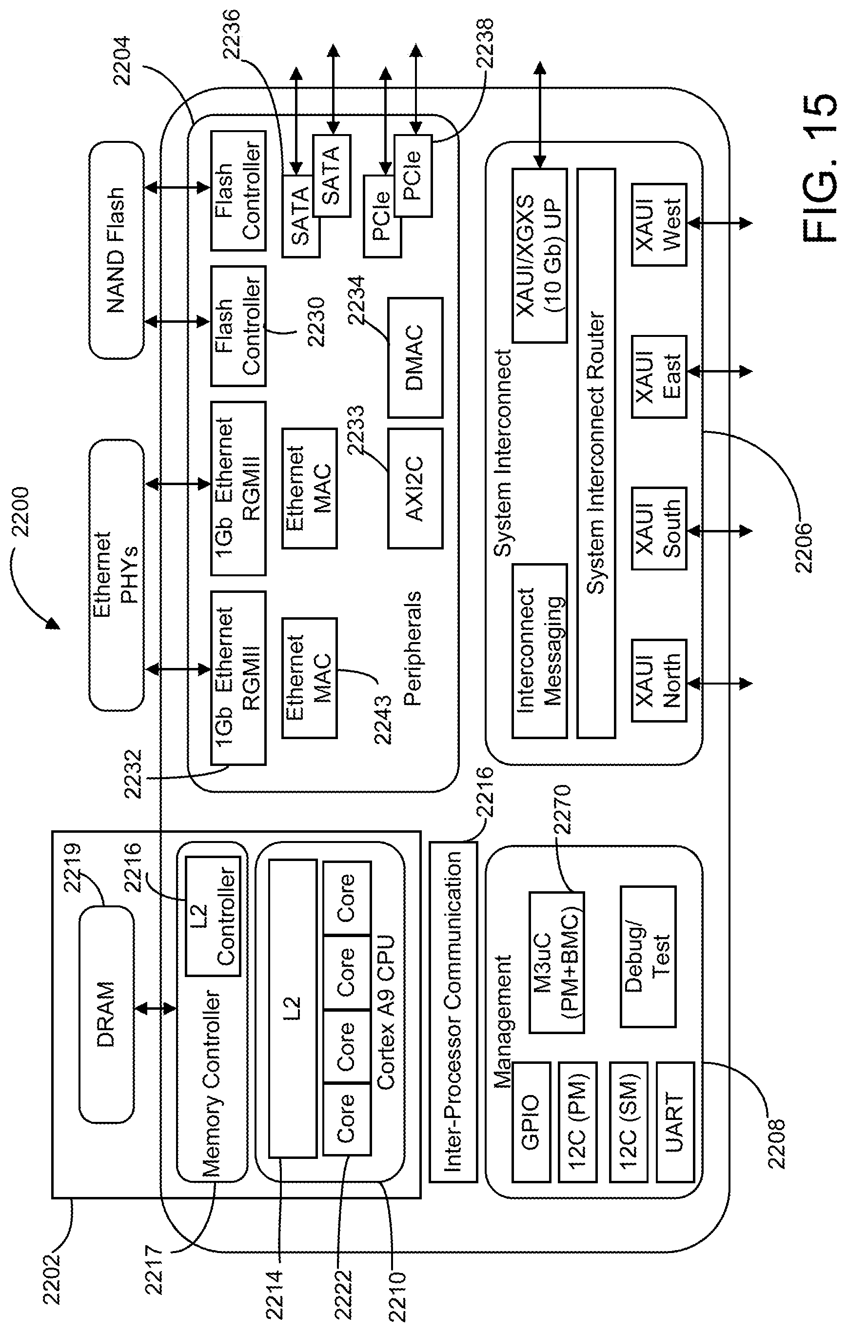
D00017

XML
uspto.report is an independent third-party trademark research tool that is not affiliated, endorsed, or sponsored by the United States Patent and Trademark Office (USPTO) or any other governmental organization. The information provided by uspto.report is based on publicly available data at the time of writing and is intended for informational purposes only.
While we strive to provide accurate and up-to-date information, we do not guarantee the accuracy, completeness, reliability, or suitability of the information displayed on this site. The use of this site is at your own risk. Any reliance you place on such information is therefore strictly at your own risk.
All official trademark data, including owner information, should be verified by visiting the official USPTO website at www.uspto.gov. This site is not intended to replace professional legal advice and should not be used as a substitute for consulting with a legal professional who is knowledgeable about trademark law.