Molecular spectroscopy cell with resonant cavity
Fruehling , et al. Sept
U.S. patent number 10,775,422 [Application Number 15/695,651] was granted by the patent office on 2020-09-15 for molecular spectroscopy cell with resonant cavity. This patent grant is currently assigned to TEXAS INSTRUMENTS INCORPORATED. The grantee listed for this patent is TEXAS INSTRUMENTS INCORPORATED. Invention is credited to Benjamin Stassen Cook, Adam Joseph Fruehling, Juan Alejandro Herbsommer, Swaminathan Sankaran.


| United States Patent | 10,775,422 |
| Fruehling , et al. | September 15, 2020 |
Molecular spectroscopy cell with resonant cavity
Abstract
A device includes a substrate that includes a resonant cavity. The resonant cavity includes a plurality of dipolar molecules that have an absorption frequency. The resonant cavity resonates at a frequency that is equal to the absorption frequency of the dipolar molecules. The device further includes a first port on the resonant cavity configured to receive a radio frequency (RF) signal.
| Inventors: | Fruehling; Adam Joseph (Garland, TX), Herbsommer; Juan Alejandro (Allen, TX), Cook; Benjamin Stassen (Addison, TX), Sankaran; Swaminathan (Allen, TX) | ||||||||||
|---|---|---|---|---|---|---|---|---|---|---|---|
| Applicant: |
|
||||||||||
| Assignee: | TEXAS INSTRUMENTS INCORPORATED
(Dallas, TX) |
||||||||||
| Family ID: | 1000005054688 | ||||||||||
| Appl. No.: | 15/695,651 | ||||||||||
| Filed: | September 5, 2017 |
Prior Publication Data
| Document Identifier | Publication Date | |
|---|---|---|
| US 20190072595 A1 | Mar 7, 2019 | |
| Current U.S. Class: | 1/1 |
| Current CPC Class: | G01N 22/00 (20130101); H03L 7/26 (20130101); G01R 23/16 (20130101); H01P 7/06 (20130101) |
| Current International Class: | G01N 22/00 (20060101); G01R 23/16 (20060101); H03L 7/26 (20060101); H01P 7/06 (20060101) |
References Cited [Referenced By]
U.S. Patent Documents
| 4147431 | April 1979 | Mann |
| 4826616 | May 1989 | Tanino |
| 5107231 | April 1992 | Knox |
| 5198786 | March 1993 | Russell et al. |
| 5218373 | June 1993 | Heckaman |
| 5412186 | May 1995 | Gale |
| 5459324 | October 1995 | Fima |
| 5821836 | October 1998 | Katehi |
| 6131256 | October 2000 | Dydyk et al. |
| 6236366 | May 2001 | Yamamoto et al. |
| 6287874 | September 2001 | Hefti |
| 6362706 | March 2002 | Song et al. |
| 6498550 | December 2002 | Miller et al. |
| 6630359 | October 2003 | Caillat et al. |
| 6670866 | December 2003 | Ella et al. |
| 6842088 | January 2005 | Yamada et al. |
| 6989723 | January 2006 | Komuro et al. |
| 6998691 | February 2006 | Baugh |
| 7388454 | June 2008 | Ruby et al. |
| 7408428 | August 2008 | Larson, III |
| 8098208 | January 2012 | Ficker et al. |
| 8268642 | September 2012 | Yoshitomi et al. |
| 8293661 | October 2012 | Yamazaki |
| 8586178 | November 2013 | Schwanke et al. |
| 9436902 | September 2016 | Koepp et al. |
| 9529334 | December 2016 | Herbsommer et al. |
| 9735754 | August 2017 | Shin et al. |
| 2002/0038989 | April 2002 | Larson, III |
| 2002/0068018 | June 2002 | Pepper |
| 2002/0098611 | July 2002 | Chang et al. |
| 2003/0015707 | January 2003 | Bosco et al. |
| 2003/0048500 | March 2003 | Fala et al. |
| 2003/0107459 | June 2003 | Takahashi et al. |
| 2004/0142484 | July 2004 | Berlin |
| 2004/0166577 | August 2004 | Storek et al. |
| 2005/0023932 | February 2005 | Inoue et al. |
| 2006/0022761 | February 2006 | Abeles |
| 2006/0076632 | April 2006 | Palmateer et al. |
| 2006/0144150 | July 2006 | Wu |
| 2007/0189359 | August 2007 | Chen et al. |
| 2008/0319285 | December 2008 | Hancock |
| 2010/0182102 | July 2010 | Kuypers et al. |
| 2010/0259334 | October 2010 | Briggs |
| 2010/0327701 | December 2010 | Grannen et al. |
| 2011/0140971 | June 2011 | Schwanke et al. |
| 2012/0266681 | October 2012 | Baumann et al. |
| 2013/0176703 | July 2013 | Hopper et al. |
| 2014/0155295 | June 2014 | Hindson et al. |
| 2014/0210835 | July 2014 | Hong et al. |
| 2014/0347074 | November 2014 | Nadeau |
| 2014/0368376 | December 2014 | Nadeau et al. |
| 2014/0368377 | December 2014 | Nadeau et al. |
| 2014/0373599 | December 2014 | Trombley et al. |
| 2015/0144297 | May 2015 | Toivonen et al. |
| 2015/0123748 | July 2015 | Stevenson |
| 2015/0277386 | October 2015 | Passilly et al. |
| 2016/0091663 | March 2016 | Taylor |
| 2016/0233178 | August 2016 | Lamy et al. |
| 2017/0073223 | March 2017 | Nasiri et al. |
| 2017/0125660 | May 2017 | Stephanou et al. |
| 2017/0130102 | May 2017 | Campbell et al. |
| 2018/0159547 | June 2018 | Herbsommer et al. |
| 6428974 | Jan 1989 | JP | |||
| WO2014037016 | Mar 2014 | WO | |||
| 2016161215 | Oct 2016 | WO | |||
Other References
|
International Search Report for PCT/US2018/050253 dated Jan. 10, 2019. cited by applicant . Alvarez, A.L. et al; "The Application of Microencapsulation Techniques in the Treatment of Endodontic and Periodontal Diseases" Pharmaceutics; 2011 abstract p. 540-548. cited by applicant . Steinberg, D. et al; "A New Degradable Controlled Release Device for Treatment of Periodontal Disease: In Vitro Release Study"; J. Periodontology; 1990; p. 393 lines 1-17; p. 394 col. 1 lines 5-14. cited by applicant . Xiong, R. et al.; "Towards Theranostic Multicompartment Microcapsules: in situ Diagnostics and Laser-induced Treatment", Theranostics; 2013; pp. 145-149. cited by applicant . International Search Report for PCT/US2018/049513 dated Nov. 15, 2018. cited by applicant . International Search Report for PCT/US2018/049940 dated Dec. 13, 2018. cited by applicant . International Search Report for PCT/US2018/049949 dated Dec. 13, 2018. cited by applicant . International Search Report for PCT/US2018/049949 dated Dec. 27, 2018. cited by applicant . International Search Report for PCT/US2018/047105 dated Dec. 27, 2018. cited by applicant. |
Primary Examiner: Monsur; Nasima
Attorney, Agent or Firm: Davis, Jr.; Michael A. Brill; Charles A. Cimino; Frank D.
Claims
What is claimed is:
1. A device, comprising: a sealing structure: a substrate attached to the sealing structure, the substrate having a cavity sealed by the sealing structure, the cavity including dipolar molecules that have an absorption frequency, and the cavity configured to resonate at the absorption frequency; a port on the substrate or the sealing structure, the port configured to receive a radio frequency (RF) signal; a transceiver; and a hybrid coupler coupled between the transceiver and the port, the transceiver coupled through the hybrid coupler to the port, and the hybrid coupler configured to provide the RF signal from the transceiver to the port, and to provide a reflected signal from the port to the transceiver, and the transceiver configured to lock a frequency of the RF signal to the absorption frequency.
2. The device of claim 1, wherein the transceiver is configured to adjust the frequency of the RF signal based on a power of the reflected signal.
3. The device of claim 1, wherein the port is a first port, and the device further comprises a second port on the substrate or the sealing structure.
4. The device of claim 3, wherein the transceiver is configured to provide the RF signal to the first port, and to adjust the frequency of the RF signal based on a signal received by the transceiver from the second port.
5. The device of claim 1, wherein the substrate is a semiconductor substrate, and the cavity has walls that are lined with a metal.
6. The device of claim 1, wherein the cavity includes a post at a center of a surface of the cavity.
7. The device of claim 1, wherein the dipolar molecules include water molecules.
8. The device of claim 1, wherein the cavity is hermetically sealed by the sealing structure.
Description
BACKGROUND
Various applications may include a sealed chamber formed in a semiconductor structure. In one particular application, a chip-scale atomic dock may include a selected vapor at a low pressure in a sealed chamber. Miniaturization of such devices while maximizing the cross-sectional area of interaction with the molecules in the chamber is a challenge.
SUMMARY
In one embodiment, a device includes a substrate that includes a resonant cavity. The resonant cavity includes a plurality of dipolar molecules that have an absorption frequency. The resonant cavity resonates at a frequency that is equal to the absorption frequency of the dipolar molecules. The device further includes a first port on the resonant cavity configured to receive a radio frequency (RF) signal.
A device includes a substrate that includes a resonant cavity. The resonant cavity includes a plurality of dipolar molecules that have an absorption frequency. The resonant cavity resonates at a frequency that is equal to the absorption frequency of the dipolar molecules. The device further includes a first port on the resonant cavity configured to receive a radio frequency (RF) signal. Further, the device includes a transceiver coupled to the first port to lock the frequency of the RF signal to the absorption frequency.
In yet another embodiment, a device includes a substrate that includes a resonant cavity. The resonant cavity includes a plurality of water molecules that have an absorption frequency. The resonant cavity resonates at a frequency that is equal to the absorption frequency of the water molecules. A first port is provided on the resonant cavity and is configured to receive a radio frequency (RF) signal. A signal generator is coupled to the first port and os configured to generate the RF signal. A power monitor is coupled to the first port to detect reflected power from the port.
BRIEF DESCRIPTION OF THE DRAWINGS
For a detailed description of various examples, reference will now be made to the accompanying drawings in which:
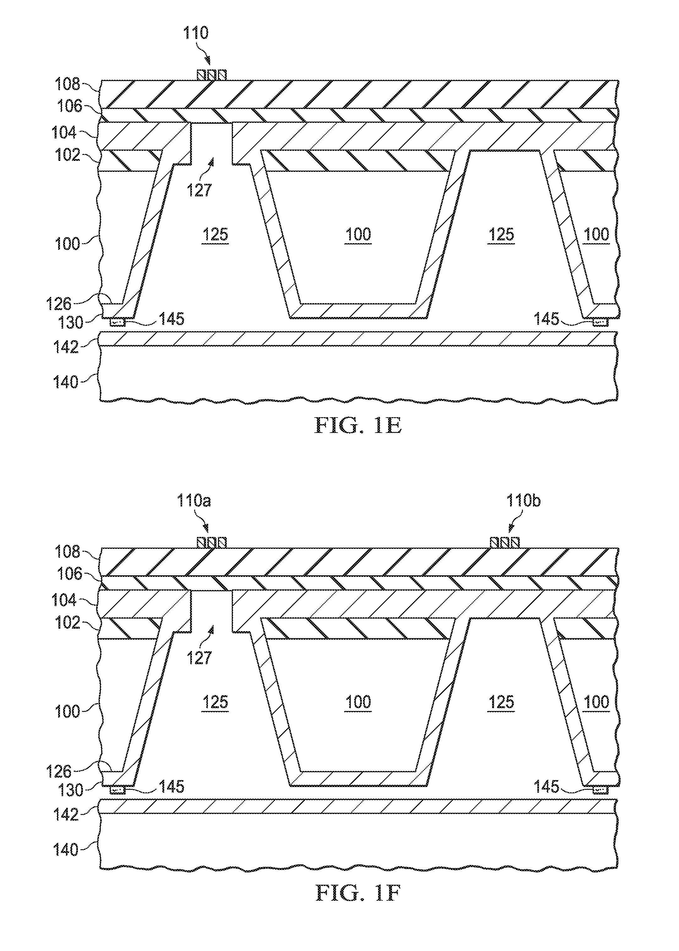
FIGS. 1A-E illustrate a sequence of operations to form a resonant cavity for a spectroscopy cell.
FIG. 1F shows an example of a multi-port resonant cavity.
FIG. 1G shows an example of a resonant cavity without a central post.
FIG. 2 shows an example of a single port resonant cavity coupled to a transceiver through a hybrid coupler in accordance with various embodiments.
FIG. 3 shows an example of a multi-port resonant cavity coupled to a transceiver in accordance with various embodiments
DETAILED DESCRIPTION
The embodiments disclosed herein are directed to a spectroscopy cell which comprises a cavity formed in a substrate such as a semiconductor substrate. The cavity contains a species of a dipolar molecule (e.g., water molecules) at a relatively low pressure. The cavity is hermetically sealed and a radio frequency (RF) signal is injected into the cavity at a frequency that approximately equals the absorption frequency of the dipolar molecules in the cavity. For water molecules, the absorption frequency is 183.31 GHz. The disclosure spectroscopy cell can be used for a variety of applications such as a clock generator to produce a clock signal at 183.31 GHz that does not vary with temperature, pressure, or process.
The pressure inside the cavity is relatively low. In the example of water molecules, the pressure may be approximately 0.1 millibars (mbars), although there is a range of acceptable pressures. If argon molecules were used, for example, the pressure may be several atmospheres. Pressures that are too high result in an increased width of the absorption peaks with respect to frequency and thus difficulty in locating the local minimum at the absorption frequency. Pressures that are too low results in so few molecules in the cavity that the signal amplitude is too small and thus the high signal-to-noise ratio is too high. In general, it is desirable to have as many molecules in the cavity to provide an acceptable signal amplitude but not so many molecules for a given size cavity that the pressure is too high for successful identification of the absorption peak.
In the disclosed embodiments, the cavity in the spectroscopy cell is a resonant cavity. As a resonant cavity, an RF signal injected into the cavity at the resonant frequency of the cavity cause the electromagnetic waves to reinforce. The quality (Q) factor of a resonant cavity can be relatively high, which increases the stability of the spectroscopy cell. In one embodiment, a spectroscopy cell is made from a semiconductor substrate that is processed to form the resonant cavity.
FIGS. 1A-E illustrate a series of steps to fabricate a spectroscopy cell. At FIG. 1A, a first oxide layer 102 is formed on a first substrate 100. A first metal layer 104 is formed on a surface of the first oxide layer 102 opposite the first substrate 100. The first metal layer 104 may comprise copper or another suitable metal. A second oxide layer 106 is formed on a surface of the first metal layer 104 opposite the first oxide layer 102. The oxide layers may comprise silicon oxide and layers 102-106 may be formed in accordance with any suitable semiconductor process operations. The substrate 100 is a semiconductor substrate (e.g., silicon) in some embodiments, but can be other than a semiconductor substrate in other embodiments, such as a ceramic or dielectric (e.g., glass) material or a three-dimensional (3D) machined metallic cavity.
At FIG. 1B, a non-conductive structure 108 is bonded (or deposited) to a surface of the second oxide layer 106 opposite the first metal layer 104. In one example, the non-conductive structure comprises glass (e.g., 130 micrometers thick), but can include other dielectric materials such as ceramics or polymers in other embodiments. The process to bond the non-conductive structure 108 to the second oxide layer 106 may comprise an anodic, fusion, eutectic solder, transition liquid phase (TLP), cofiring, or other suitable bonding processes. In some embodiments, non-conductive structure 108 may be bonded directly to first metal layer 104 without the need of the second oxide layer 106.
FIG. 1C illustrates that an antenna 110 has been patterned on a surface of the non-conductive structure 108. The antenna 110 comprises a conductive material such as copper or gold and an electrical RF signal can be provided to the antenna. In some embodiments, the resonant cavity is a single-port cavity having antenna 110, but in other embodiments, the resonant cavity includes multiple ports with one antenna for each port. For a multi-port cavity, one port is used to inject an RF signal into the resonant cavity, and the other port is used to monitor the signal from the cavity. FIG. 1F illustrates an example of a multi-port cavity with antennas 110a and 110b.
FIG. 1D illustrates that a cavity 125 has been created in the substrate 100. The cavity 125 may be wet etched into the substrate 120 using a suitable wet etchant such as potassium hydroxide (KOH) or tetramethylammonium hydroxide (TMAH). The cavity 125 is etched from the surface 126 of the substrate 100 opposite the first oxide layer 102 to the first oxide layer 102, thereby exposing a portion of the first oxide layer 102. The cavity may be formed in a circular, square, rectangular or other cross-sectional shape. In the embodiment of FIG. 1D, the cavity is formed around a center post 129 such that the post occupies a portion of the center of the cavity 125. The post 129 is a portion of the substrate 100 that was not etched away when forming the cavity 125. The central frequency of the cavity can be tuned through selection of the post dimensions. In one example, an unloaded (no post) 4 mm diameter by 0.5 mm tall octagonal cavity provides a resonant frequency of approximately 60 GHz. With the introduction of a central post having a base diameter of 1.75 mm, and sidewall profile tapered in accordance with the etched crystal planes, the resonant frequency can be reduced to approximately 6 GHz with a gap between the conductive surface (metal layer 130, discussed below) on the post 129 and the conductive surface (metal layer 142, discussed below) on the substrate 140 of 3.5 micron. Any intermediate frequency is achievable by design of the post gap between a few microns and the full cavity depth and can be further tuned with the post diameter. In addition, this can increase the maximum electric field strength in the region of the post by orders of magnitude. In other embodiments, the cavity 125 does not include a central post. The cavity 125 in FIG. 1D also illustrates that another metal layer 130 has been deposited on a surface of the substrate 100 opposite the first oxide layer 102. The metal layer 130 is deposited in the cavity 125 as shown and in some examples may be sputter deposited (e.g. 40 nm Ti or Cr and 1 um of Cu or Au)
Referring still to FIG. 1D, an iris 127 is formed in the metal layer 130 generally adjacent the antenna 110. The iris 127 is patterned in the metal layer 130 and exposes at least a portion of the second oxide layer 106. The iris 140 permits the RF energy from the incident radio frequency (RF) signal provided by the antenna 110 is able to penetrate through the iris 127 and into the cavity 125.
FIG. 1E shows a second substrate 140 and a metal layer 142 formed thereon. The substrate 140 may comprise the same or different material as substrate 100. In one example, the substrate 140 comprises a semiconductor substrate such as a portion of a silicon wafer, but can be other than a semiconductor material in other examples (e.g. ceramic, kovar/invar, or other 3D manufactured metal structures). Bonding structures 145 are deposited and patterned on either or both of the substrates 100 and 140. In one example, the bonding structures comprise a gold, aluminum, silicon or other types of material that form an alloy when heated to a suitable temperature. The resulting structure includes a hermetically sealed resonator cavity. Dipolar molecules (e.g., water molecules) may be trapped inside the cavity 125 and at an internal pressure of approximately 0.1 mbars, although there can be a range of pressure in various applications.
Some embodiments do not include the center post in the cavity. FIG. 1G shows an example of a resonant cavity without the center post.
The shape and size of the cavity 125 can vary between embodiments. In general, the cavity is sized to resonate at a particular frequency, or range of frequencies. The size of the cavity scales with the frequency. To achieve resonant frequencies in the sub-10 GHz range, the cavity will grow quite large (on the order of cm). As demonstrated above, this dimension can be dramatically reduced with post loading. For example, an octagonal cavity etched in silicon resonating near 180 GHz would have a diameter of approximately 2.75 mm on the top of the cavity & 2.2 mm at the bottom. However, mode selection and excitation structures play a significant role in the sizing of the cavity. The resonant frequency of the cavity 125 includes the absorption frequency of the particular dipolar molecule species trapped inside the cavity (e.g., 183.31 GHz for water molecules).
As noted above, the spectroscopy cell includes a resonant cavity that has either only one port or multiple ports. FIG. 2 illustrates an embodiment of a single port resonant cavity 200. The resonant cavity 200 includes a port 202. Port 202 is coupled to a transceiver 210 through a hybrid coupler 212. The transceiver 210, which includes a signal generator and a power monitor, generates an RF signal at frequency that is approximately equal to the absorption frequency of the dipolar molecules in the cavity 200. The hybrid coupler 212 provides the RF signal to the port 202 on the cavity and receives reflected signals from the cavity as well. The transceiver 210 receives a signal indicative of the reflected signals and computes the reflected power from the port, which is indicative of how close the RF signal generated by the transceiver is to the absorption frequency of the molecule species in the cavity. The closer the RF frequency is to the absorption frequency, the lower will be reflected power from the cavity. The transceiver 210 uses the magnitude of the reflected power as a feedback signal to lock on to the absorption frequency of the molecules in the cavity.
FIG. 3 illustrates a two-port resonant cavity 300. The cavity includes a first port 302 and a second port 304. A transceiver 310 (which includes a signal generator) is connected to both ports 302 and 304. The transceiver 310 generates an RF signal and injects the RF signal into the resonant cavity through port 302. The transceiver 310 monitors the signal from port 304. The transceiver can sweep the frequency of the RF signal about the frequency known to be the absorption frequency of the cavity's dipolar molecules. At the absorption peak, the magnitude of the output signal (e.g., voltage) from the second port 304 is a minimum voltage compared to the output signal at other frequencies. The transceiver 310 uses the signal from port 304 to maintain a lock on the absorption frequency of the dipolar molecule species in the resonant cavity.
Certain terms are used throughout the above description and claims to refer to particular system components. As one skilled in the art will appreciate, different parties may refer to a component by different names. This document does not intend to distinguish between components that differ in name but not function. In the above discussion and in the claims, the terms "including" and "comprising" are used in an open-ended fashion, and thus should be interpreted to mean "including, but not limited to . . . ." Also, the term "couple" or "couples" is intended to mean either an indirect or direct wired or wireless connection. Thus, if a first device couples to a second device, that connection may be through a direct connection or through an indirect connection via other devices and connections. The recitation "based on" is intended to mean "based at least in part on." Therefore, if X is based on Y, X may be a function of Y and any number of other factors.
The above discussion is meant to be illustrative of the principles and various embodiments of the present invention. Numerous variations and modifications will become apparent to those skilled in the art once the above disclosure is fully appreciated. It is intended that the following claims be interpreted to embrace all such variations and modifications.
* * * * *
D00000
D00001
D00002
D00003
D00004
XML
uspto.report is an independent third-party trademark research tool that is not affiliated, endorsed, or sponsored by the United States Patent and Trademark Office (USPTO) or any other governmental organization. The information provided by uspto.report is based on publicly available data at the time of writing and is intended for informational purposes only.
While we strive to provide accurate and up-to-date information, we do not guarantee the accuracy, completeness, reliability, or suitability of the information displayed on this site. The use of this site is at your own risk. Any reliance you place on such information is therefore strictly at your own risk.
All official trademark data, including owner information, should be verified by visiting the official USPTO website at www.uspto.gov. This site is not intended to replace professional legal advice and should not be used as a substitute for consulting with a legal professional who is knowledgeable about trademark law.