Sense amplifier
Wang , et al. Sep
U.S. patent number 10,770,161 [Application Number 16/211,524] was granted by the patent office on 2020-09-08 for sense amplifier. This patent grant is currently assigned to MEDIATEK INC.. The grantee listed for this patent is MEDIATEK Inc.. Invention is credited to Yi-Te Chiu, Shu-Lin Lai, Chia-Wei Wang.

| United States Patent | 10,770,161 |
| Wang , et al. | September 8, 2020 |
Sense amplifier
Abstract
A sense amplifier for reading a via Read-Only Memory (Via-ROM) is provided. The sense amplifier includes a read circuit, an adaptive keeper circuit and a leakage monitor circuit. The read circuit is connected to the via-ROM. The adaptive keeper circuit is connected to the read circuit. The leakage monitor circuit is connected to the adaptive keeper circuit for forming a current mirror, such that the adaptive keeper circuit compensates a read voltage of a memory cell whose via is opened when a bit-line leakage is happened.
| Inventors: | Wang; Chia-Wei (Fengyuan, TW), Lai; Shu-Lin (Taichung, TW), Chiu; Yi-Te (Kaohsiung, TW) | ||||||||||
|---|---|---|---|---|---|---|---|---|---|---|---|
| Applicant: |
|
||||||||||
| Assignee: | MEDIATEK INC. (Hsin-Chu,
TW) |
||||||||||
| Family ID: | 1000005043848 | ||||||||||
| Appl. No.: | 16/211,524 | ||||||||||
| Filed: | December 6, 2018 |
Prior Publication Data
| Document Identifier | Publication Date | |
|---|---|---|
| US 20190108890 A1 | Apr 11, 2019 | |
Related U.S. Patent Documents
| Application Number | Filing Date | Patent Number | Issue Date | ||
|---|---|---|---|---|---|
| 15492014 | Apr 20, 2017 | 10181358 | |||
| 62412881 | Oct 26, 2016 | ||||
| Current U.S. Class: | 1/1 |
| Current CPC Class: | G11C 7/067 (20130101); G11C 7/06 (20130101); G11C 17/18 (20130101) |
| Current International Class: | G11C 17/00 (20060101); G11C 7/06 (20060101); G11C 17/18 (20060101) |
| Field of Search: | ;365/94 |
References Cited [Referenced By]
U.S. Patent Documents
| 5568438 | October 1996 | Penchuk |
| 5889702 | March 1999 | Gaultier et al. |
| 6445367 | September 2002 | Suzuki et al. |
| 6759877 | July 2004 | Desai et al. |
| 6844750 | January 2005 | Hsu et al. |
| 6982591 | January 2006 | Abadeer et al. |
| 7002375 | February 2006 | Hsu et al. |
| 7162652 | January 2007 | Issa et al. |
| 7256621 | August 2007 | Lih et al. |
| 7332937 | February 2008 | Hsu |
| 7417469 | August 2008 | Cheng |
| 7474132 | January 2009 | Cheng |
| 7479807 | January 2009 | Cheng |
| 7772890 | August 2010 | Marshall |
| 7804330 | September 2010 | Bhat |
| 7928769 | April 2011 | Huang |
| 8295116 | October 2012 | Chen et al. |
| 8441381 | May 2013 | Bajdechi et al. |
| 8482316 | July 2013 | Liu et al. |
| 8599623 | December 2013 | Clark |
| 8742823 | June 2014 | Seth |
| 9058046 | June 2015 | Pilo et al. |
| 9082465 | July 2015 | Ganesan |
| 9418761 | August 2016 | Arslan et al. |
| 9537485 | January 2017 | Puckett et al. |
| 9625924 | April 2017 | Atallah et al. |
| 9761286 | September 2017 | Fritsch |
| 9818474 | November 2017 | Hsu |
| 9940992 | April 2018 | Atallah |
| 10043578 | August 2018 | Lai |
| 10181358 | January 2019 | Wang |
| 10193536 | January 2019 | Agarwal |
| 2004/0189337 | September 2004 | Hsu et al. |
| 2004/0189347 | September 2004 | Hsu et al. |
| 2004/0228183 | November 2004 | Ito |
| 2006/0214695 | September 2006 | Lih |
| 2007/0146013 | June 2007 | Hsu |
| 2007/0252613 | November 2007 | Hsu et al. |
| 2008/0111616 | May 2008 | Cheng |
| 2008/0129346 | June 2008 | Cheng |
| 2008/0248251 | October 2008 | Ghyselen et al. |
| 2009/0015294 | January 2009 | Cheng |
| 2009/0096485 | April 2009 | Marshall |
| 2010/0073030 | March 2010 | Bhat |
| 2010/0073990 | March 2010 | Siau et al. |
| 2011/0026354 | February 2011 | Lin et al. |
| 2011/0292753 | December 2011 | Hsu et al. |
| 2012/0182056 | July 2012 | Dally |
| 2016/0172059 | June 2016 | Arslan et al. |
| 2017/0278564 | September 2017 | Hsu |
| 2017/0287550 | October 2017 | Atallah |
Other References
|
TIPO Office Action dated May 22, 2015, issued in application No. 106136936. cited by applicant. |
Primary Examiner: Nguyen; Viet Q
Attorney, Agent or Firm: McClure, Qualey & Rodack, LLP
Parent Case Text
This application is a Continuation Application of U.S. application Ser. No. 15/492,014, filed Apr. 20, 2017, now U.S. Pat. No. 10,181,358, which claims the benefit of U.S. provisional application Ser. No. 62/412,881, filed Oct. 26, 2016, the disclosure of which is incorporated by reference herein in its entirety.
Claims
What is claimed is:
1. A sense amplifier, for reading a via Read-Only Memory (Via-ROM), comprising: a read circuit connected to the via-ROM; an adaptive keeper circuit connected to the read circuit; a leakage monitor circuit connected to the adaptive keeper circuit for forming a current mirror, such that the adaptive keeper circuit compensates a read voltage of a memory cell whose via is opened when a bit-line leakage is happened; wherein the current mirror is formed by a part of the leakage monitor circuit and a part of the adaptive keeper circuit; and another part of the leakage monitor circuit and the read circuit are substantially the same.
2. The sense amplifier according to claim 1, wherein a leakage current of the leakage monitor circuit and a driving of the adaptive keeper circuit have a positive relationship.
3. The sense amplifier according to claim 1, wherein a gate of a transistor of the leakage monitor circuit is connected to a gate of a transistor of the adaptive keeper circuit.
4. The sense amplifier according to claim 1, wherein the leakage monitor circuit and the read circuit are substantially the same.
5. The sense amplifier according to claim 1, wherein a number of dummy cells connected to the leakage monitor circuit is programmed.
6. A sense amplifier, for reading a via Read-Only Memory (Via-ROM), comprising: a read circuit connected to the via-ROM; a hybrid keeper circuit connected to the read circuit, wherein the hybrid keeper circuit includes: a static keeper circuit; and an adaptive keeper circuit, wherein the static keeper circuit and the adaptive keeper circuit are connected in parallel; and a leakage monitor circuit connected to the adaptive keeper circuit for forming a current mirror, such that the adaptive keeper circuit compensates a read voltage of a memory cell whose via is opened when a bit-line leakage is happened.
7. The sense amplifier according to claim 6, wherein a driving of the static keeper circuit is less than a driving of the adaptive keeper circuit.
8. The sense amplifier according to claim 6, wherein a leakage current of the leakage monitor circuit and a driving of the adaptive keeper circuit have a positive relationship.
9. The sense amplifier according to claim 6, wherein a gate of a transistor of the leakage monitor circuit is connected to a gate of a transistor of the adaptive keeper circuit.
10. The sense amplifier according to claim 6, wherein the leakage monitor circuit and the read circuit are substantially the same.
11. The sense amplifier according to claim 6, wherein a number of dummy cells connected to the leakage monitor circuit is programmed.
12. A sense amplifier, for reading a via Read-Only Memory (Via-ROM), comprising: a read circuit connected to the via-ROM; a static keeper circuit connected to the read circuit; a leakage monitor circuit connected to the read circuit for forming a current mirror, such that a read voltage of a memory cell whose via is opened is compensated when a bit-line leakage is happened; wherein the current mirror is formed by a part of the leakage monitor circuit and a part of the read circuit; and another part of the leakage monitor circuit and another part of the read circuit are substantially the same.
13. The sense amplifier according to claim 12, wherein a gate of a transistor of the leakage monitor circuit is connected to a gate of a transistor of the read circuit.
14. The sense amplifier according to claim 12, wherein the leakage monitor circuit and the read circuit are substantially the same.
15. The sense amplifier according to claim 12, wherein a number of dummy cells connected to the leakage monitor circuit is programmed.
Description
TECHNICAL FIELD
The disclosure relates in general to a sense amplifier, and more particularly to a sense amplifier for reading a via Read-Only Memory (Via-ROM).
BACKGROUND
Along with the development of semiconductor technology, various memories are invented. Via Read-Only Memory (Via-ROM) records data by vias. Please refer to FIG. 1, which shows an example a Via-ROM 900. The via-ROM 900 includes a plurality of word lines WL9, a plurality of bit lines BL9 and a plurality of memory cells, such as code-0 cells C90 and code-1 cells C91. The source of the code-0 cell C90 is connected to the ground, a via at the drain of the code-0 cell C90 is conducted, and the read voltage of the code-0 cell C90 is ground. The source of the code-1 cell C91 is connected to the ground, a via at the drain of the code-1 cell C91 is opened, and the read voltage of the code-1 cell C91 is high.
The read voltage of one selected code-1 cell C91 may be dropped due to the bit-line leakages happened on the other code-0 cells C90. If a large number of code-0 cells C90 are formed on one bit line, the read voltage of the code-1 cell C91 on this bit line may be greatly dropped and cannot be accurately identified.
Especially, the bit-line leakages are easily happened at high speed via-ROM or high temperature environment and the read voltage of the code-1 cell C91 cannot be accurately identified. Therefore, how to compensate the read voltage under the bit-line leakage is an important issue nowadays.
SUMMARY
The disclosure is directed to a sense amplifier for reading a via Read-Only Memory (Via-ROM). An adaptive keeper is used to adaptively compensates a read voltage of a memory cell whose via is opened when a bit-line leakage is happened.
According to one embodiment, a sense amplifier for reading a via Read-Only Memory (Via-ROM) is provided. The sense amplifier includes a read circuit, an adaptive keeper circuit and a leakage monitor circuit. The read circuit is connected to the via-ROM. The adaptive keeper circuit is connected to the read circuit. The leakage monitor circuit is connected to the adaptive keeper circuit for forming a current mirror, such that the adaptive keeper circuit compensates a read voltage of a memory cell whose via is opened when a bit-line leakage is happened.
According to another embodiment, a sense amplifier for reading a via Read-Only Memory (Via-ROM) is provided. The sense amplifier includes a read circuit, a hybrid keeper circuit and a leakage monitor circuit. The read circuit is connected to the via-ROM. The hybrid keeper circuit is connected to the read circuit. The hybrid keeper circuit includes a static keeper circuit and an adaptive keeper circuit. The static keeper circuit and the adaptive keeper circuit are connected in parallel. The leakage monitor circuit is connected to the adaptive keeper circuit for forming a current mirror, such that the adaptive keeper circuit compensates a read voltage of a memory cell whose via is opened when a bit-line leakage is happened.
According to alternative another embodiment, a sense amplifier for reading a via Read-Only Memory (Via-ROM) is provided. The sense amplifier includes a read circuit, a static keeper circuit and a leakage monitor circuit. The read circuit is connected to the via-ROM. The static keeper circuit is connected to the read circuit. The leakage monitor circuit is connected to the read circuit for forming a current mirror, such that a read voltage of a memory cell whose via is opened is compensated when a bit-line leakage is happened.
BRIEF DESCRIPTION OF THE DRAWINGS
FIG. 1 (prior art) shows an example a Via-ROM.
FIG. 2 shows a sense amplifier according one embodiment.
FIG. 3 shows a sense amplifier according another embodiment.
FIG. 4 shows a sense amplifier according another embodiment.
In the following detailed description, for purposes of explanation, numerous specific details are set forth in order to provide a thorough understanding of the disclosed embodiments. It will be apparent, however, that one or more embodiments may be practiced without these specific details. In other instances, well-known structures and devices are schematically shown in order to simplify the drawing.
DETAILED DESCRIPTION
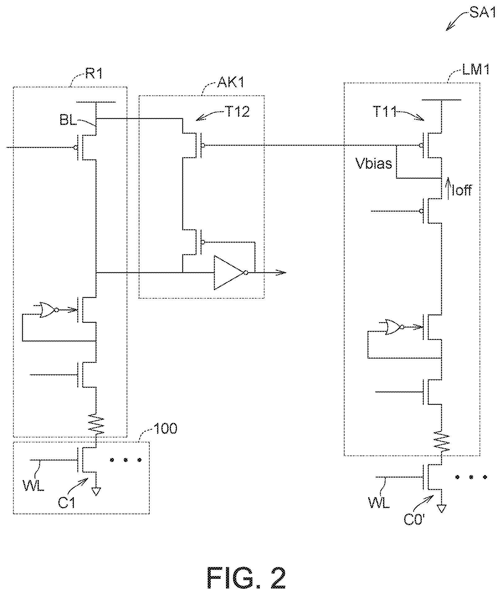
Please refer to FIG. 2, which shows a sense amplifier SA1 according one embodiment. The sense amplifier SA1 is used for reading a via Read-Only Memory (Via-ROM) 100. The sense amplifier SA1 includes a read circuit R1, an adaptive keeper circuit AK1 and a leakage monitor circuit LM1. The read circuit R1 is connected to the Via-ROM 100. The adaptive keeper circuit AK1 is connected to the read circuit R1. The leakage monitor circuit LM1 is connected to the adaptive keeper circuit AK1.
The read circuit R1 is used for reading the read voltage of one memory cell of the Via-ROM 100, such as a code-1 cell C1 whose via is opened, or a code-0 cell (not shown) whose via is conducted. The code-1 cell C1 is connected to a word line WL and a bit line BL. Because the via of the code-1 cell C1 is opened, the read voltage of the code-1 cell C1 should be high. However, when the bit-line leakage is happened, the read voltage of the code-1 cell C1 may be dropped.
The leakage monitor circuit LM1 is used for providing a leakage current Ioff. The leakage monitor circuit LM1 and the adaptive keeper circuit AK1 are connected to form a current mirror, such that the adaptive keeper circuit AK1 compensates the read voltage of the code-1 cell C1 when the bit-line leakage is happened.
The leakage current Ioff of the leakage monitor circuit LM1 and a driving of the adaptive keeper circuit AK1 have a positive relationship. If the temperature is high or the speed of the Via-ROM is high, the bit-line leakage is easily happened. The leakage current Ioff of the leakage monitor circuit LM1 is high and the driving of the adaptive keeper circuit AK1 is high. Therefore, even if the read voltage of the code-1 cell C1 is greatly dropped due to the bit-line leakage, the adaptive keeper circuit AK1 has enough driving ability to compensate the read voltage of the code-1 cell C1.
If the temperature is low or the speed of the Via-ROM 100 is low, the bit-line leakage is not easily happened. The leakage current Ioff of the leakage monitor circuit LM1 is low and the driving of the adaptive keeper circuit AK1 is low. Therefore, when the read voltage of the code-1 cell C1 is not dropped or is slightly dropped due to the bit-line leakage, the adaptive keeper circuit AK1 has low driving ability to slightly compensate the read voltage of the code-1 cell C1.
Further, when a code-0 cell (not shown) is read, the adaptive keeper circuit AK1 has low driving ability or no driving ability, such that the read voltage of the code-0 cell (not shown) can be accurately dropped to be ground. Thus, even if the bit-line leakages are happened at high speed via-ROM or high temperature environment and the read voltages of the code-1 cell C1 and the code-0 cell (not shown) can be accurately identified respectively.
Referring to FIG. 2, a gate of a transistor T11 of the leakage monitor circuit LM1 is connected to a gate of a transistor T12 of the adaptive keeper circuit AK1, and the gate of the transistor T11 is connected to the source/drain of the transistor T11. A bias voltage Vbias of the transistor T11 drives the transistor T12 to be turned on.
In this embodiment, the leakage monitor circuit LM1 and the read circuit R1 are substantially the same. The leakage monitor circuit LM1 is connected to a plurality of dummy cells, such as a plurality of code-0 cells C0'. Each gate of the code-0 cells C0' is connected to a dummy word line WL' which is grounded. Therefore, the leakage current Ioff can be simulated.
In one embodiment, the number of the dummy cells may range from 64 to 512, such as 64, 128, 511 or 512. The number of dummy cells connected to the leakage monitor circuit LM1 is programmed.
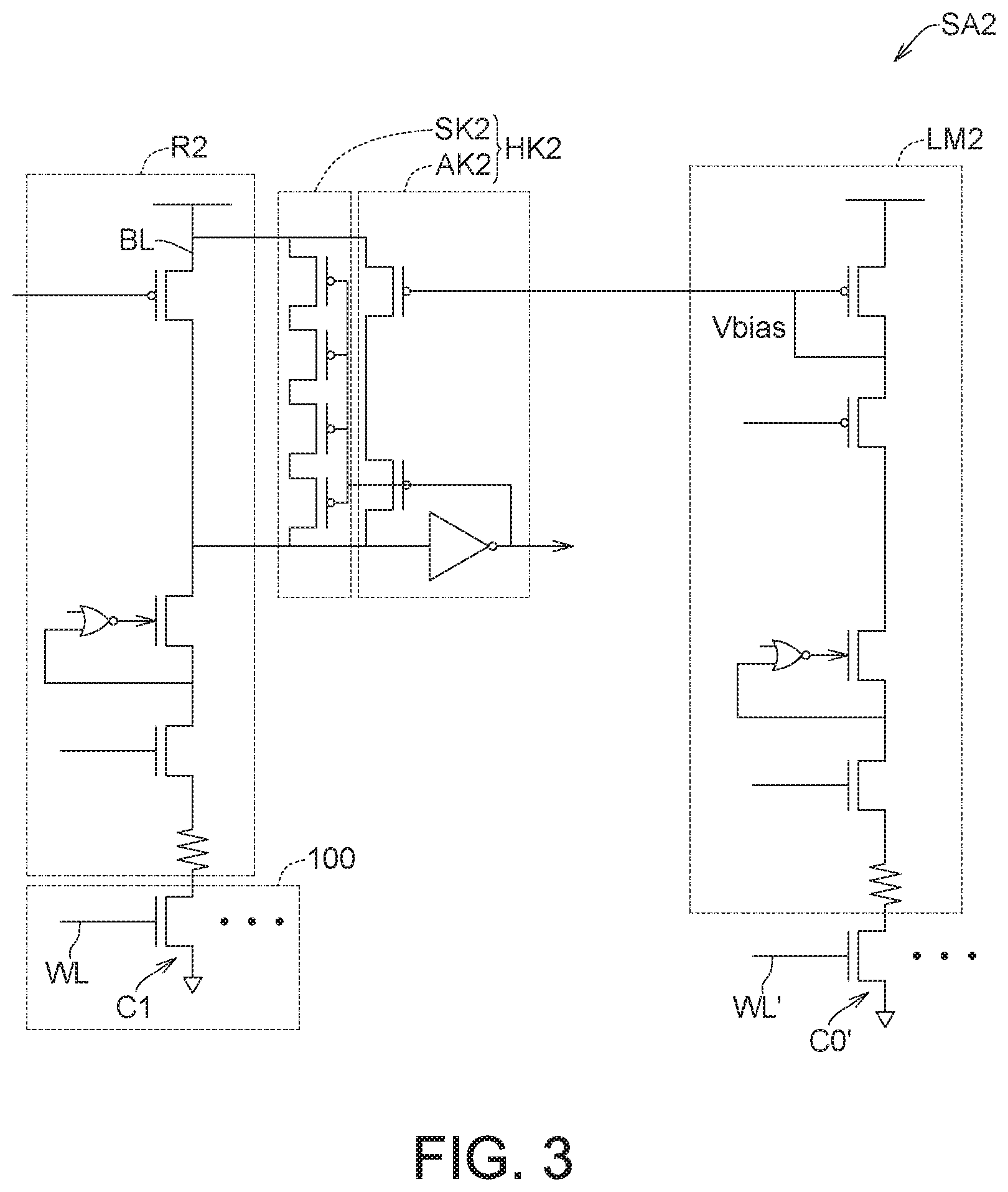
Please refer to FIG. 3, which show a sense amplifier SA2 according to another embodiment. In this embodiment, the sense amplifier SA2 includes a read circuit R2, a hybrid keeper circuit HK2 and a leakage monitor circuit LM2. The read circuit R2 is similar to the read circuit R1, the leakage monitor circuit LM2 is similar to the leakage monitor LM1, and the similarities are not repeated here. The hybrid keeper circuit HK2 is connected to the read circuit R2 and includes a static keeper circuit SK2 and an adaptive keeper circuit AK2. The static keeper circuit SK2 and the adaptive keeper circuit AK2 are connected in parallel.
In this embodiment, the leakage monitor circuit LM2 and the read circuit R2 are substantially the same. The leakage monitor circuit LM2 is connected to several dummy cells, such as the code-0 cells C0'. Each gate of the code-0 cells C0' is connected to the dummy word line WL' which is grounded. Therefore, the leakage current Ioff can be simulated.
The leakage current Ioff of the leakage monitor circuit LM2 and a driving of the adaptive keeper circuit AK2 have a positive relationship. If the temperature is high or the speed of the Via-ROM is high, the bit-line leakage is easily happened. The leakage current Ioff of the leakage monitor circuit LM2 is high and the driving of the adaptive keeper circuit AK2 is high. Therefore, even if the read voltage of the code-1 cell C1 is greatly dropped due to the bit-line leakage, the adaptive keeper circuit AK2 has enough driving ability to compensate the read voltage of the code-1 cell C1.
If the temperature is low or the speed of the Via-ROM 100 is low, the bit-line leakage is not easily happened. The leakage current Ioff of the leakage monitor circuit LM2 is low and the driving of the adaptive keeper circuit AK2 is turned off. Therefore, when the read voltage of the code-1 cell C1 is not dropped, the adaptive keeper circuit AK2 has no driving ability and will not compensate the read voltage of the code-1 cell C1.
Further, when a code-0 cell (not shown) is read, the adaptive keeper circuit AK2 has no driving ability, such that the read voltage of the code-0 cell (not shown) can be accurately dropped to be ground.
In this embodiment, the driving of the static keeper circuit SK2 is less than the driving of the adaptive keeper circuit AK2. The static keeper circuit SK2 is used for assisting the adaptive keeper circuit AK2 at the low temperature.
For example, if the temperature is low, the leakage current Ioff of the leakage monitor circuit LM2 is low and the driving of the adaptive keeper circuit AK2 is low. Even if the driving of the adaptive keeper circuit AK2 is lowered, the static keeper circuit SK2 still can compensate the read voltage of the code-1 cell C1. Thus, even if the bit-line leakages are happened at high speed via-ROM or high temperature environment and the read voltages of the code-1 cell C1 and the code-0 cell (not shown) can be accurately identified respectively.
In one embodiment, the number of the dummy cells may range from 64 to 512, such as 64, 128, 511 or 512. The number of dummy cells connected to the leakage monitor circuit LM2 is programmed.
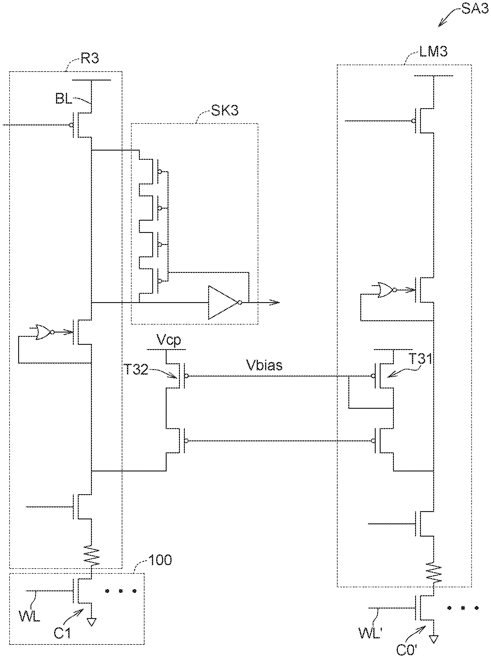
Please referring to FIG. 4, which shows a sense amplifier SA3 according to another embodiment. The sense amplifier SA3 includes a read circuit R3, a static keeper circuit SK3 and a leakage monitor circuit LM3. The static keeper circuit SK3 is connected to the read circuit R3 to compensate the read voltage of the code-1 cell C1 when the bit-line leakage is happened.
Further, in this embodiment, the leakage monitor circuit LM3 is connected to the read circuit R3 for forming a current mirror. A gate of a transistor T31 of the leakage monitor circuit LM3 is connected to a gate of a transistor T32 of the read circuit R3. When the bit-line leakage is happened, a bias voltage Vbias of the transistor T31 drives the transistor T32 to be turned on, such that a compensation voltage Vcp can compensate the read voltage of the code-1 cell C1. Thus, even if the bit-line leakages are happened at high speed via-ROM or high temperature environment and the read voltages of the code-1 cell C1 and the code-0 cell (not shown) can be accurately identified respectively.
It will be apparent to those skilled in the art that various modifications and variations can be made to the disclosed embodiments. It is intended that the specification and examples be considered as exemplary only, with a true scope of the disclosure being indicated by the following claims and their equivalents.
* * * * *
D00000
D00001
D00002
D00003
D00004
XML
uspto.report is an independent third-party trademark research tool that is not affiliated, endorsed, or sponsored by the United States Patent and Trademark Office (USPTO) or any other governmental organization. The information provided by uspto.report is based on publicly available data at the time of writing and is intended for informational purposes only.
While we strive to provide accurate and up-to-date information, we do not guarantee the accuracy, completeness, reliability, or suitability of the information displayed on this site. The use of this site is at your own risk. Any reliance you place on such information is therefore strictly at your own risk.
All official trademark data, including owner information, should be verified by visiting the official USPTO website at www.uspto.gov. This site is not intended to replace professional legal advice and should not be used as a substitute for consulting with a legal professional who is knowledgeable about trademark law.