Micro-transfer printed LED and color filter structures
Cok , et al.
U.S. patent number 10,692,844 [Application Number 15/990,305] was granted by the patent office on 2020-06-23 for micro-transfer printed led and color filter structures. This patent grant is currently assigned to X Display Company Technology Limited. The grantee listed for this patent is X Display Company Technology Limited. Invention is credited to Christopher Andrew Bower, Ronald S. Cok.


View All Diagrams
| United States Patent | 10,692,844 |
| Cok , et al. | June 23, 2020 |
Micro-transfer printed LED and color filter structures
Abstract
A micro-transfer printed intermediate structure comprises an intermediate substrate and one or more pixel structures disposed on the intermediate substrate. Each pixel structure includes an LED, a color filter, and a fractured pixel tether physically attached to the pixel structure. A fractured intermediate tether is physically attached to the intermediate substrate. A method of making an intermediate structure source wafer comprises providing a source wafer having a patterned sacrificial layer including sacrificial portions separated by anchors, disposing an intermediate substrate over the patterned sacrificial layer, and disposing one or more pixel structures on the intermediate substrate entirely on or over each sacrificial portion. Each pixel structure includes an LED, a color filter, and a fractured pixel tether physically attached to the pixel structure to form an intermediate structure.
| Inventors: | Cok; Ronald S. (Rochester, NY), Bower; Christopher Andrew (Raleigh, NC) | ||||||||||
|---|---|---|---|---|---|---|---|---|---|---|---|
| Applicant: |
|
||||||||||
| Assignee: | X Display Company Technology
Limited (Dublin, IE) |
||||||||||
| Family ID: | 59959759 | ||||||||||
| Appl. No.: | 15/990,305 | ||||||||||
| Filed: | May 25, 2018 |
Prior Publication Data
| Document Identifier | Publication Date | |
|---|---|---|
| US 20180277525 A1 | Sep 27, 2018 | |
Related U.S. Patent Documents
| Application Number | Filing Date | Patent Number | Issue Date | ||
|---|---|---|---|---|---|
| 15461871 | Mar 17, 2017 | 10008483 | |||
| 62318512 | Apr 5, 2016 | ||||
| Current U.S. Class: | 1/1 |
| Current CPC Class: | H01L 24/00 (20130101); H01L 25/0753 (20130101); H01L 33/0095 (20130101); H01L 25/50 (20130101); H01L 33/505 (20130101); H01L 2933/0025 (20130101); H01L 33/502 (20130101); H01L 2933/0041 (20130101) |
| Current International Class: | H01L 25/075 (20060101); H01L 33/00 (20100101); H01L 25/00 (20060101); H01L 33/50 (20100101); H01L 23/00 (20060101) |
References Cited [Referenced By]
U.S. Patent Documents
| 4746202 | May 1988 | Perilloux et al. |
| 5060027 | October 1991 | Hart et al. |
| 5550066 | August 1996 | Tang et al. |
| 5621555 | April 1997 | Park |
| 5625202 | April 1997 | Chai |
| 5748161 | May 1998 | Lebby et al. |
| 5815303 | September 1998 | Berlin |
| 5886401 | March 1999 | Liu |
| 5917572 | June 1999 | Kurauchi et al. |
| 5994722 | November 1999 | Averbeck et al. |
| 6025730 | February 2000 | Akram et al. |
| 6084579 | July 2000 | Hirano |
| 6087680 | July 2000 | Gramann et al. |
| 6142358 | November 2000 | Cohn et al. |
| 6143672 | November 2000 | Ngo et al. |
| 6169294 | January 2001 | Biing-Jye et al. |
| 6184477 | February 2001 | Tanahashi |
| 6278242 | August 2001 | Cok et al. |
| 6288824 | September 2001 | Kastalsky |
| 6340999 | January 2002 | Masuda et al. |
| 6392340 | May 2002 | Yoneda et al. |
| 6403985 | June 2002 | Fan et al. |
| 6410942 | June 2002 | Thibeault et al. |
| 6466281 | October 2002 | Huang et al. |
| 6504180 | January 2003 | Heremans et al. |
| 6577367 | June 2003 | Kim |
| 6650382 | November 2003 | Sumida et al. |
| 6660457 | December 2003 | Imai et al. |
| 6703780 | March 2004 | Shiang et al. |
| 6717560 | April 2004 | Cok et al. |
| 6756576 | June 2004 | McElroy et al. |
| 6812637 | November 2004 | Cok et al. |
| 6825559 | November 2004 | Mishra et al. |
| 6828724 | December 2004 | Burroughes |
| 6881946 | April 2005 | Cok et al. |
| 6933532 | August 2005 | Arnold et al. |
| 6969624 | November 2005 | Iwafuchi et al. |
| 6975369 | December 2005 | Burkholder |
| 7009220 | March 2006 | Oohata |
| 7012382 | March 2006 | Cheang et al. |
| 7091523 | August 2006 | Cok et al. |
| 7098589 | August 2006 | Erchak et al. |
| 7127810 | October 2006 | Kasuga et al. |
| 7129457 | October 2006 | McElroy et al. |
| 7157838 | January 2007 | Thielemans et al. |
| 7195733 | March 2007 | Rogers et al. |
| 7259391 | August 2007 | Liu et al. |
| 7288753 | October 2007 | Cok |
| 7329905 | February 2008 | Ibbetson et al. |
| 7394194 | July 2008 | Cok |
| 7402951 | July 2008 | Cok |
| 7408296 | August 2008 | Cok et al. |
| 7417648 | August 2008 | Credelle |
| 7420221 | September 2008 | Nagai |
| 7466075 | December 2008 | Cok et al. |
| 7521292 | April 2009 | Rogers et al. |
| 7557367 | July 2009 | Rogers et al. |
| 7586497 | September 2009 | Boroson et al. |
| 7605053 | October 2009 | Couillard et al. |
| 7614757 | November 2009 | Nesterenko et al. |
| 7622367 | November 2009 | Nuzzo et al. |
| 7629955 | December 2009 | Asao et al. |
| 7662545 | February 2010 | Nuzzo et al. |
| 7687812 | March 2010 | Louwsma et al. |
| 7704684 | April 2010 | Rogers et al. |
| 7791271 | September 2010 | Cok et al. |
| 7799699 | September 2010 | Nuzzo et al. |
| 7816856 | October 2010 | Cok et al. |
| 7834541 | November 2010 | Cok |
| 7872722 | January 2011 | Kimura |
| 7893612 | February 2011 | Cok |
| 7898734 | March 2011 | Coleman et al. |
| 7919342 | April 2011 | Cok |
| 7927976 | April 2011 | Menard |
| 7932123 | April 2011 | Rogers et al. |
| 7943491 | May 2011 | Nuzzo et al. |
| 7948172 | May 2011 | Cok et al. |
| 7969085 | June 2011 | Cok |
| 7972875 | July 2011 | Rogers et al. |
| 7982296 | July 2011 | Nuzzo et al. |
| 7990058 | August 2011 | Cok et al. |
| 7999454 | August 2011 | Winters et al. |
| 8004758 | August 2011 | Coleman et al. |
| 8029139 | October 2011 | Ellinger et al. |
| 8039847 | October 2011 | Nuzzo et al. |
| 8058663 | November 2011 | Fan et al. |
| 8198621 | June 2012 | Rogers et al. |
| 8207547 | June 2012 | Lin |
| 8243027 | August 2012 | Hotelling et al. |
| 8261660 | September 2012 | Menard |
| 8288843 | October 2012 | Kojima et al. |
| 8334545 | December 2012 | Levermore et al. |
| 8394706 | March 2013 | Nuzzo et al. |
| 8440546 | May 2013 | Nuzzo et al. |
| 8450927 | May 2013 | Lenk et al. |
| 8470701 | June 2013 | Rogers et al. |
| 8502192 | August 2013 | Kwak et al. |
| 8506867 | August 2013 | Menard |
| 8536584 | September 2013 | Yao |
| 8558243 | October 2013 | Bibl et al. |
| 8581827 | November 2013 | Park et al. |
| 8596846 | December 2013 | Yankov et al. |
| 8619011 | December 2013 | Kimura |
| 8664699 | March 2014 | Nuzzo et al. |
| 8686447 | April 2014 | Tomoda et al. |
| 8722458 | May 2014 | Rogers et al. |
| 8735932 | May 2014 | Kim et al. |
| 8754396 | June 2014 | Rogers et al. |
| 8759865 | June 2014 | Tsai et al. |
| 8766970 | July 2014 | Chien et al. |
| 8791474 | July 2014 | Bibl et al. |
| 8794501 | August 2014 | Bibl et al. |
| 8803857 | August 2014 | Cok |
| 8817369 | August 2014 | Daiku |
| 8829663 | September 2014 | Pohl et al. |
| 8835940 | September 2014 | Hu et al. |
| 8836624 | September 2014 | Roberts et al. |
| 8854294 | October 2014 | Sakariya |
| 8860051 | October 2014 | Fellows et al. |
| 8877648 | November 2014 | Bower et al. |
| 8884844 | November 2014 | Yang et al. |
| 8889485 | November 2014 | Bower |
| 8895406 | November 2014 | Rogers et al. |
| 8901578 | December 2014 | Kobayakawa et al. |
| 8902152 | December 2014 | Bai et al. |
| 8912020 | December 2014 | Bedell et al. |
| 8946760 | February 2015 | Kim |
| 8987765 | March 2015 | Bibl et al. |
| 9022632 | May 2015 | Kim et al. |
| 9048449 | June 2015 | Kim et al. |
| 9105714 | August 2015 | Hu et al. |
| 9105813 | August 2015 | Chang |
| 9139425 | September 2015 | Vestyck |
| 9153171 | October 2015 | Sakariya et al. |
| 9161448 | October 2015 | Menard et al. |
| 9178123 | November 2015 | Sakariya et al. |
| 9202996 | December 2015 | Orsley et al. |
| 9226361 | December 2015 | Toth |
| 9277618 | March 2016 | Odnoblyudov et al. |
| 9293422 | March 2016 | Parsa et al. |
| 9308649 | April 2016 | Golda et al. |
| 9329430 | May 2016 | Erinjippurath et al. |
| 9343042 | May 2016 | Miller et al. |
| 9358775 | June 2016 | Bower et al. |
| 9362348 | June 2016 | Lowenthal et al. |
| 9368683 | June 2016 | Meitl et al. |
| 9412977 | August 2016 | Rohatgi |
| 9437782 | September 2016 | Bower et al. |
| 9444015 | September 2016 | Bower et al. |
| 9478583 | October 2016 | Hu et al. |
| 9520537 | December 2016 | Bower et al. |
| 9537069 | January 2017 | Bower et al. |
| 9590025 | March 2017 | Yu et al. |
| 9601356 | March 2017 | Bower et al. |
| 9626908 | April 2017 | Sakariya et al. |
| 9634191 | April 2017 | Keller et al. |
| 9640715 | May 2017 | Bower et al. |
| 9698308 | July 2017 | Bower et al. |
| 9705042 | July 2017 | Bower et al. |
| 9716082 | July 2017 | Bower et al. |
| 9741785 | August 2017 | Bower et al. |
| 9847047 | December 2017 | Wu et al. |
| 9860955 | January 2018 | Kim et al. |
| 9871345 | January 2018 | Bower et al. |
| 9929053 | March 2018 | Bower et al. |
| 9980341 | May 2018 | Bower et al. |
| 9991163 | June 2018 | Bower et al. |
| 9997501 | June 2018 | Bower et al. |
| 10008483 | June 2018 | Cok |
| 10078239 | September 2018 | Sugita et al. |
| 10103069 | October 2018 | Bower et al. |
| 10199546 | February 2019 | Cok |
| 10209813 | February 2019 | Yao et al. |
| 2001/0022564 | September 2001 | Youngquist et al. |
| 2002/0096994 | July 2002 | Iwafuchi et al. |
| 2002/0118321 | August 2002 | Ge |
| 2002/0126194 | September 2002 | Okabe et al. |
| 2002/0140646 | October 2002 | Sato et al. |
| 2002/0171792 | November 2002 | Kubota et al. |
| 2002/0171801 | November 2002 | Hsieh et al. |
| 2003/0001165 | January 2003 | Taki |
| 2004/0080483 | April 2004 | Chosa |
| 2004/0080941 | April 2004 | Jiang et al. |
| 2004/0180476 | September 2004 | Kazlas et al. |
| 2004/0206970 | October 2004 | Martin |
| 2004/0212296 | October 2004 | Nakamura et al. |
| 2004/0227704 | November 2004 | Wang et al. |
| 2004/0252933 | December 2004 | Sylvester et al. |
| 2005/0006657 | January 2005 | Terashita |
| 2005/0012076 | January 2005 | Morioka |
| 2005/0116621 | June 2005 | Bellmann et al. |
| 2005/0140275 | June 2005 | Park |
| 2005/0168987 | August 2005 | Tamaoki et al. |
| 2005/0202595 | September 2005 | Yonehara et al. |
| 2005/0264472 | December 2005 | Rast |
| 2005/0275615 | December 2005 | Kahen et al. |
| 2005/0285246 | December 2005 | Haba et al. |
| 2006/0051900 | March 2006 | Shizuno |
| 2006/0063309 | March 2006 | Sugiyama et al. |
| 2006/0180818 | August 2006 | Nagai et al. |
| 2006/0273862 | December 2006 | Shimmura |
| 2006/0289972 | December 2006 | Nishimura et al. |
| 2007/0035340 | February 2007 | Kimura |
| 2007/0077349 | April 2007 | Newman et al. |
| 2007/0182809 | August 2007 | Yarid et al. |
| 2007/0201056 | August 2007 | Cok et al. |
| 2008/0108171 | May 2008 | Rogers et al. |
| 2008/0112069 | May 2008 | Helber |
| 2008/0211734 | September 2008 | Huitema et al. |
| 2008/0296717 | December 2008 | Beroz et al. |
| 2009/0045420 | February 2009 | Eng et al. |
| 2009/0146921 | June 2009 | Takahashi |
| 2009/0278142 | November 2009 | Watanabe et al. |
| 2009/0284696 | November 2009 | Cheong et al. |
| 2009/0295706 | December 2009 | Feng |
| 2009/0315054 | December 2009 | Kim et al. |
| 2010/0038655 | February 2010 | Chen et al. |
| 2010/0060553 | March 2010 | Zimmerman et al. |
| 2010/0078670 | April 2010 | Kim et al. |
| 2010/0123134 | May 2010 | Nagata |
| 2010/0123268 | May 2010 | Menard |
| 2010/0148198 | June 2010 | Sugizaki et al. |
| 2010/0149117 | June 2010 | Chien et al. |
| 2010/0186883 | July 2010 | Tomoda |
| 2010/0190293 | July 2010 | Maeda et al. |
| 2010/0201253 | August 2010 | Cok et al. |
| 2010/0207852 | August 2010 | Cok |
| 2010/0214245 | August 2010 | Hirota |
| 2010/0214247 | August 2010 | Tang et al. |
| 2010/0225673 | September 2010 | Miller |
| 2010/0248484 | September 2010 | Bower et al. |
| 2010/0258710 | October 2010 | Wiese et al. |
| 2010/0270912 | October 2010 | Ko |
| 2010/0289115 | November 2010 | Akiyama et al. |
| 2010/0317132 | December 2010 | Rogers et al. |
| 2010/0321414 | December 2010 | Muroi et al. |
| 2010/0328268 | December 2010 | Teranishi et al. |
| 2011/0032277 | February 2011 | Lee et al. |
| 2011/0043435 | February 2011 | Hebenstreit et al. |
| 2011/0069013 | March 2011 | Rabenstein et al. |
| 2011/0108800 | May 2011 | Pan |
| 2011/0120678 | May 2011 | Palm |
| 2011/0205448 | August 2011 | Takata |
| 2011/0211348 | September 2011 | Kim |
| 2011/0242027 | October 2011 | Chang |
| 2011/0309378 | December 2011 | Lau et al. |
| 2011/0316008 | December 2011 | Yokogawa |
| 2012/0018745 | January 2012 | Liu et al. |
| 2012/0056835 | March 2012 | Choo et al. |
| 2012/0062135 | March 2012 | Tamaki et al. |
| 2012/0105518 | May 2012 | Kang et al. |
| 2012/0119249 | May 2012 | Kim et al. |
| 2012/0126229 | May 2012 | Bower |
| 2012/0141799 | June 2012 | Kub et al. |
| 2012/0154713 | June 2012 | Kwon |
| 2012/0193652 | August 2012 | Horng et al. |
| 2012/0206428 | August 2012 | Cok |
| 2012/0206499 | August 2012 | Cok |
| 2012/0212465 | August 2012 | White et al. |
| 2012/0223636 | September 2012 | Shin et al. |
| 2012/0223875 | September 2012 | Lau et al. |
| 2012/0228669 | September 2012 | Bower et al. |
| 2012/0236022 | September 2012 | Homma et al. |
| 2012/0256163 | October 2012 | Yoon et al. |
| 2012/0274669 | November 2012 | Neal |
| 2012/0281028 | November 2012 | Orlick et al. |
| 2012/0314388 | December 2012 | Bower et al. |
| 2012/0320308 | December 2012 | Yeo et al. |
| 2012/0320566 | December 2012 | Namekata |
| 2012/0320581 | December 2012 | Rogers et al. |
| 2013/0006524 | January 2013 | Sasaki et al. |
| 2013/0010405 | January 2013 | Rothkopf et al. |
| 2013/0015483 | January 2013 | Shimokawa et al. |
| 2013/0016494 | January 2013 | Speier et al. |
| 2013/0036928 | February 2013 | Rogers et al. |
| 2013/0069275 | March 2013 | Menard et al. |
| 2013/0088416 | April 2013 | Smith et al. |
| 2013/0153277 | June 2013 | Menard et al. |
| 2013/0161667 | June 2013 | Chen et al. |
| 2013/0196474 | August 2013 | Meitl et al. |
| 2013/0207964 | August 2013 | Fleck et al. |
| 2013/0221355 | August 2013 | Bower et al. |
| 2013/0248889 | September 2013 | Lin |
| 2013/0257264 | October 2013 | Tamaki et al. |
| 2013/0273695 | October 2013 | Menard et al. |
| 2013/0278513 | October 2013 | Jang |
| 2013/0309792 | November 2013 | Tischler et al. |
| 2014/0014960 | January 2014 | Yamazaki et al. |
| 2014/0027724 | January 2014 | Lim |
| 2014/0082934 | March 2014 | Cok |
| 2014/0084482 | March 2014 | Hu et al. |
| 2014/0085214 | March 2014 | Cok |
| 2014/0094878 | April 2014 | Gossler et al. |
| 2014/0104157 | April 2014 | Burns et al. |
| 2014/0104243 | April 2014 | Sakariya et al. |
| 2014/0111442 | April 2014 | Cok et al. |
| 2014/0146273 | May 2014 | Kim et al. |
| 2014/0159043 | June 2014 | Sakariya et al. |
| 2014/0159065 | June 2014 | Hu et al. |
| 2014/0175399 | June 2014 | Choi |
| 2014/0175498 | June 2014 | Lai |
| 2014/0183446 | July 2014 | Nago et al. |
| 2014/0192079 | July 2014 | Lee et al. |
| 2014/0197509 | July 2014 | Haddad et al. |
| 2014/0198373 | July 2014 | Ray |
| 2014/0217448 | August 2014 | Kim et al. |
| 2014/0231839 | August 2014 | Jeon et al. |
| 2014/0231851 | August 2014 | Tsai et al. |
| 2014/0240617 | August 2014 | Fukutome et al. |
| 2014/0264763 | September 2014 | Meitl et al. |
| 2014/0267683 | September 2014 | Bibl et al. |
| 2014/0291641 | October 2014 | Negishi |
| 2014/0306248 | October 2014 | Ahn et al. |
| 2014/0319486 | October 2014 | Hong |
| 2014/0339495 | November 2014 | Bibl et al. |
| 2014/0340900 | November 2014 | Bathurst et al. |
| 2014/0367633 | December 2014 | Bibl et al. |
| 2014/0367705 | December 2014 | Bibl et al. |
| 2015/0003040 | January 2015 | Bessho et al. |
| 2015/0015517 | January 2015 | Zhao |
| 2015/0021632 | January 2015 | Taghizadeh et al. |
| 2015/0034934 | February 2015 | Rohatgi |
| 2015/0084054 | March 2015 | Fan et al. |
| 2015/0135525 | May 2015 | Bower |
| 2015/0137153 | May 2015 | Bibl et al. |
| 2015/0169011 | June 2015 | Bibl et al. |
| 2015/0170602 | June 2015 | Kang |
| 2015/0179453 | June 2015 | Cheng et al. |
| 2015/0255438 | September 2015 | Oraw et al. |
| 2015/0263066 | September 2015 | Hu et al. |
| 2015/0263256 | September 2015 | Hsieh et al. |
| 2015/0279822 | October 2015 | Hsu |
| 2015/0280066 | October 2015 | Fujimura et al. |
| 2015/0280089 | October 2015 | Obata et al. |
| 2015/0296580 | October 2015 | Kim et al. |
| 2015/0308634 | October 2015 | van de Ven et al. |
| 2015/0318328 | November 2015 | Bibl et al. |
| 2015/0327388 | November 2015 | Menard et al. |
| 2015/0362165 | December 2015 | Chu et al. |
| 2015/0370130 | December 2015 | Lin |
| 2015/0371585 | December 2015 | Bower et al. |
| 2015/0371974 | December 2015 | Bower et al. |
| 2015/0372051 | December 2015 | Bower et al. |
| 2015/0372052 | December 2015 | Bower et al. |
| 2015/0372053 | December 2015 | Bower et al. |
| 2015/0372187 | December 2015 | Bower et al. |
| 2015/0373793 | December 2015 | Bower et al. |
| 2016/0004123 | January 2016 | Tanabe |
| 2016/0005721 | January 2016 | Bower et al. |
| 2016/0018094 | January 2016 | Bower et al. |
| 2016/0056725 | February 2016 | Kim et al. |
| 2016/0057822 | February 2016 | Chu |
| 2016/0057827 | February 2016 | Miskin |
| 2016/0057832 | February 2016 | Briggs et al. |
| 2016/0064363 | March 2016 | Bower et al. |
| 2016/0085120 | March 2016 | Xu |
| 2016/0093600 | March 2016 | Bower et al. |
| 2016/0103547 | April 2016 | Lu et al. |
| 2016/0131329 | May 2016 | Park et al. |
| 2016/0210895 | July 2016 | Fan et al. |
| 2016/0211245 | July 2016 | Do |
| 2016/0260388 | September 2016 | Yata et al. |
| 2016/0266697 | September 2016 | Cheng et al. |
| 2016/0343772 | November 2016 | Bower et al. |
| 2016/0351539 | December 2016 | Bower et al. |
| 2016/0364030 | December 2016 | Peana et al. |
| 2016/0370855 | December 2016 | Lanier et al. |
| 2017/0005244 | January 2017 | Bower et al. |
| 2017/0010706 | January 2017 | Cok |
| 2017/0025075 | January 2017 | Cok et al. |
| 2017/0025395 | January 2017 | Chen et al. |
| 2017/0025484 | January 2017 | Forrest et al. |
| 2017/0047393 | February 2017 | Bower et al. |
| 2017/0048976 | February 2017 | Prevatte et al. |
| 2017/0061842 | March 2017 | Cok et al. |
| 2017/0068362 | March 2017 | Den Boer et al. |
| 2017/0092863 | March 2017 | Bower et al. |
| 2017/0102797 | April 2017 | Cok |
| 2017/0122502 | May 2017 | Cok et al. |
| 2017/0133818 | May 2017 | Cok |
| 2017/0148771 | May 2017 | Cha et al. |
| 2017/0167703 | June 2017 | Cok |
| 2017/0186740 | June 2017 | Cok et al. |
| 2017/0187976 | June 2017 | Cok |
| 2017/0206845 | July 2017 | Sakariya et al. |
| 2017/0221266 | August 2017 | Schubert et al. |
| 2017/0250167 | August 2017 | Bower et al. |
| 2017/0250219 | August 2017 | Bower et al. |
| 2017/0256521 | September 2017 | Cok et al. |
| 2017/0256522 | September 2017 | Cok et al. |
| 2017/0287882 | October 2017 | Cok et al. |
| 2017/0338374 | November 2017 | Zou et al. |
| 2017/0352646 | December 2017 | Bower et al. |
| 2017/0352647 | December 2017 | Raymond et al. |
| 2017/0357127 | December 2017 | Cok et al. |
| 2017/0358717 | December 2017 | Cok et al. |
| 2018/0007750 | January 2018 | Meitl et al. |
| 2018/0033853 | February 2018 | Bower et al. |
| 2018/0041005 | February 2018 | Bower et al. |
| 2018/0174932 | June 2018 | Cok et al. |
| 2018/0175248 | June 2018 | Ahmed |
| 2018/0197471 | July 2018 | Rotzoll et al. |
| 2018/0211945 | July 2018 | Cok et al. |
| 2018/0226386 | August 2018 | Cok |
| 2018/0323180 | November 2018 | Cok |
| 2018/0340681 | November 2018 | Cok |
| 2018/0366450 | December 2018 | Gardner et al. |
| 2019/0027534 | January 2019 | Rotzoll et al. |
| 2019/0148604 | May 2019 | Cok et al. |
| 103677427 | Mar 2014 | CN | |||
| 105992994 | Oct 2016 | CN | |||
| 1662301 | May 2006 | EP | |||
| 1843194 | Oct 2007 | EP | |||
| 2078978 | Jul 2009 | EP | |||
| 2148264 | Jan 2010 | EP | |||
| 2 610 314 | Jul 2013 | EP | |||
| 2703969 | Mar 2014 | EP | |||
| 2 496 183 | May 2013 | GB | |||
| 11-142878 | May 1999 | JP | |||
| 2010-103186 | May 2010 | JP | |||
| 2013-221965 | Oct 2013 | JP | |||
| WO-2006/027730 | Mar 2006 | WO | |||
| WO-2006/099741 | Sep 2006 | WO | |||
| WO-2008/103931 | Aug 2008 | WO | |||
| WO-2010/032603 | Mar 2010 | WO | |||
| WO-2010/111601 | Sep 2010 | WO | |||
| WO-2010/132552 | Nov 2010 | WO | |||
| WO-2013/011415 | Jan 2013 | WO | |||
| WO-2013/064800 | May 2013 | WO | |||
| WO-2013/165124 | Nov 2013 | WO | |||
| WO-2014/121635 | Aug 2014 | WO | |||
| WO-2014/149864 | Sep 2014 | WO | |||
| WO-2015/088629 | Jun 2015 | WO | |||
| WO-2015/193434 | Dec 2015 | WO | |||
| WO-2016/030422 | Mar 2016 | WO | |||
| WO-2016/046283 | Mar 2016 | WO | |||
| WO-2017/042252 | Mar 2017 | WO | |||
| WO-2017/149067 | Sep 2017 | WO | |||
| WO-2017/174632 | Oct 2017 | WO | |||
Other References
|
US. Appl. No. 14/788,632, filed Jun. 30, 2015, X-Celeprint Limited. cited by applicant . U.S. Appl. No. 14/807,311, filed Jul. 23, 2015, X-Celeprint Limited. cited by applicant . U.S. Appl. No. 14/822,866, filed Aug. 10, 2015, Bower et al. cited by applicant . Choi, H. W. et al., Efficient GaN-based Micro-LED Arrays, Mat. Res. Soc. Symp. Proc. 743:L6.28.1-L6.28.6 (2003). cited by applicant . Cok, R. S. et al., AMOLED displays with transfer-printed integrated circuits, Journal of SID 19/(4):335-341 (2011). cited by applicant . Hamer et al., 63.2: AMOLED Displays Using Transfer-Printed Integrated Circuits, SID 09 Digest, 40(2):947-950 (2009). cited by applicant . International Search Report, PCT/EP2017/058066, 3 pages, dated Jul. 5, 2017. cited by applicant . Johnson, K. et al., Advances in Red VCSEL Technology, Advances in Optical Technologies, 2012:569379, 13 pages (2012). cited by applicant . Kasahara, D. et al, Nichia reports first room-temperature blue/`green` VCSELs with current injection, Appl. Phys. Express, 4(7):3 pages (2011). cited by applicant . Koma, N. et al., 44.2: Novel Front-light System Using Fine-pitch Patterned OLED, SID, 08:655-658 (2008). cited by applicant . Lee, S. H. etal, Laser Lift-Offof GaN Thin Film and its Application to the Flexible Light Emitting Diodes, Proc. of SPIE 8460:846011-1-846011-6 (2012). cited by applicant . Matioli, E. et al., High-brightness polarized light-emitting diodes, Light: Science & Applications, 1:e22:1-7 (2012). cited by applicant . Poher, V. et al., Micro-LED arrays: a tool for two-dimensional neuron stimulation, J. Phys. D: Appl. Phys. 41:094014 (2008). cited by applicant . Roscher, H., VCSEL Arrays with Redundant Pixel Designs for 10Gbits/s 2-D Space-Parallel MMF Transmission, Annual Report, optoelectronics Department, (2005). cited by applicant . Seurin, J.F. et al, High-power red VCSEL arrays, Proc. of SPIE 8639:1-9 (2013). cited by applicant . Written Opinion, PCT/EP2017/058066, 8 pages, dated Jul. 5, 2017. cited by applicant . Yaniv et al., A 640 x 480 Pixel Computer Display Using Pin Diodes with Device Redundancy, 1988 International Display Research Conference, IEEE, CH-2678-1/88:152-154 (1988). cited by applicant . Yoon, J. et al., Heterogeneously Integrated Optoelectronic Devices Enabled by MicroTransfer Printing, Adv. Optical Mater. 3:1313-1335 (2015). cited by applicant . Bower, C. A. et al., Transfer Printing: An Approach for Massively Parallel Assembly of Microscale Devices, IEE, Electronic Components and Technology Conference, (2008). cited by applicant . Cok, R. S. et al., 60.3: AMOLED Displays Using Transfer-Printed Integrated Circuits, Society for Information Display, 10:902-904, (2010). cited by applicant . Feng, X. et al., Competing Fracture in Kinetically Controlled Transfer Printing, Langmuir, 23(25):12555-12560, (2007). cited by applicant . Gent, A.N., Adhesion and Strength of Viscoelastic Solids. Is There a Relationship between Adhesion and Bulk Properties?, American Chemical Society, Langmuir, 12(19):4492-4496, (1996). cited by applicant . Kim, Dae-Hyeong et al., Optimized Structural Designs for Stretchable Silicon Integrated Circuits, Small, 5(24):2841-2847, (2009). cited by applicant . Kim, Dae-Hyeong et al., Stretchable and Foldable Silicon Integrated Circuits, Science, 320:507-511, (2008). cited by applicant . Kim, S. et al., Microstructural elastomeric surfaces with reversible adhesion and examples of their use in deterministic assembly by transfer printing, PNAS, 107(40):17095-17100 (2010). cited by applicant . Kim, T. et al., Kinetically controlled, adhesiveless transfer printing using microstructured stamps, Applied Physics Letters, 94(11):113502-1-113502-3, (2009). cited by applicant . Meitl, M. A. et al., Transfer printing by kinetic control of adhesion to an elastomeric stamp, Nature Material, 5:33-38, (2006). cited by applicant . Michel, B. et al., Printing meets lithography: Soft approaches to high-resolution patterning, J. Res. & Dev. 45(5):697-708, (2001). cited by applicant . Trindade, A.J. et al., Precision transfer printing of ultra-thin AlInGaN micron-size light-emitting diodes, Crown, pp. 217-218, (2012). cited by applicant . Cok, R. S. et al., Inorganic light-emitting diode displays using micro-transfer printing, Journal of the SID, 25(10):589-609, (2017). cited by applicant . Bower, C. A. et al., Micro-Transfer-Printing: Heterogeneous Integration of Microscale Semiconductor Devices using Elastomer Stamps, 2014 IEEE Sensors, 3 pages and 1 page IEEE Xplore abstract, date of conference: Nov. 2-5, 2014. cited by applicant. |
Primary Examiner: Gebreyesus; Yosef
Attorney, Agent or Firm: Haulbrook; William R. Schmitt; Michael D. Choate, Hall & Stewart LLP
Parent Case Text
PRIORITY APPLICATIONS
This application is a continuation of U.S. patent application Ser. No. 15/461,871, filed Mar. 17, 2017, entitled Micro-Transfer Printed LED and Color Filter Structure, which claims priority to and benefit of U.S. Patent Application No. 62/318,512, filed Apr. 5, 2016, entitled Micro-Transfer Printed LED and Color Filter Structure, the content of each of which is hereby incorporated by reference in its entirety.
Claims
The invention claimed is:
1. A micro-transfer printed color-filter structure, comprising: a color filter; and a fractured color-filter tether attached to the color filter or layers formed in contact with the color filter.
2. The color filter of claim 1, wherein the color filter is or includes one or more of: a curable resin, a dye, a pigment, a color-conversion material, a semiconductor crystal, a phosphor, and a quantum dot.
3. The color filter of claim 1, wherein the fractured color-filter tether includes at least some of the same material as the color filter.
4. The color-filter structure of claim 1, further comprising an encapsulation layer, wherein the fractured color-filter tether includes at least some of the same material as the encapsulation layer or at least a portion of the encapsulation layer forms the color-filter tether.
5. The color-filter structure of claim 1, wherein the color filter is constructed to filter light.
6. The color-filter structure of claim 1, wherein the color filter is constructed to convert light.
7. A micro-transfer printed pixel structure, comprising: an LED having a light-emitting side; a color filter disposed adjacent to the light-emitting side of the LED; and a fractured pixel tether physically attached (i) to the LED, (ii) to layers disposed on or in contact with the LED, (iii) to the color filter, or (iv) to layers disposed on the color filter.
8. The pixel structure of claim 7, wherein the color filter is or includes one or more of: a curable resin, a dye, a pigment, a color conversion material, a semiconductor crystal, a phosphor, and a quantum dot.
9. The pixel structure of claim 7, wherein the fractured pixel tether includes at least some of the same material as the color filter, wherein the fractured pixel tether includes at least some of the same material as the LED, or both.
10. A light-emitting diode (LED) display, comprising: a display substrate; and a plurality of micro-transfer printed pixel structures according to claim 7 disposed on the display substrate, wherein the LED of each of the micro-transfer printed pixel structures is an inorganic LEDs.
11. The LED display of claim 10, wherein the corresponding color filter is located between the display substrate and the corresponding inorganic LED.
12. The LED display of claim 10, wherein each of the one or more inorganic LEDs is located between the display substrate and the corresponding color filter.
13. The LED display of claim 10, wherein the corresponding color filter is constructed to filter light.
14. The LED display of claim 10, wherein the corresponding color filter is constructed to convert light.
15. The micro-transfer printed pixel structure of claim 7, comprising an encapsulation layer encapsulating the LED and the color filter, wherein the encapsulation layer forms the fractured pixel tether or the fractured pixel tether is a part of or is attached to the encapsulation layer.
16. A micro-transfer printed intermediate structure, comprising: an intermediate substrate; one or more pixel structures disposed on or over the intermediate substrate, each of the one or more pixel structures including an LED having a light-emitting side, a color filter disposed adjacent to the light-emitting side of the LED, and a fractured pixel tether physically attached to the pixel structure; and a fractured intermediate tether physically attached to the intermediate substrate or physically attached to a layer disposed on the intermediate substrate.
17. The intermediate structure of claim 16, wherein: (i) the color filter is or includes one or more of: a curable resin, a dye, a pigment, a color conversion material, a semiconductor crystal, a phosphor, or a quantum dot; (ii) the intermediate substrate is or includes a glass, a polymer, a semiconductor, or silicon; or both (i) and (ii).
18. The intermediate structure of claim 16, wherein the fractured pixel tether includes at least some of the same material as the color filter or wherein the fractured pixel tether includes at least some of the same material as the LED, or both.
19. The intermediate structure of claim 16, wherein the fractured intermediate tether includes at least some of the same material as the color filter or wherein the fractured intermediate tether includes at least some of the same material as the intermediate substrate, or both.
20. The intermediate structure of claim 16, comprising an encapsulation layer encapsulating the color filter and LED, wherein the fractured pixel tether includes at least some of the same material as the encapsulation layer or at least a portion of the encapsulation layer forms the fractured pixel tether or the fractured pixel tether is a part of or is attached to the encapsulation layer.
21. The intermediate structure of claim 16, comprising an encapsulation layer encapsulating the color filter and LED, wherein the fractured intermediate tether includes at least some of the same material as the encapsulation layer or at least a portion of the encapsulation layer forms the fractured intermediate tether or the fractured intermediate tether is a part of or is attached to the encapsulation layer.
22. A light-emitting diode (LED) display, comprising: a display substrate; and a plurality of pixel structures disposed on the display substrate, each of the plurality of pixel structures comprising one or more LEDs and a corresponding color filter corresponding to each of the one or more LEDs, wherein the one or more LEDs each have a light-emitting side and the corresponding color filter is disposed adjacent to the light-emitting side of the corresponding LED, wherein said each of the one or more LEDs is a micro-transfer printed LED and a fractured LED tether is physically attached to the LED.
23. A light-emitting diode (LED) display, comprising: a display substrate; and a plurality of pixel structures disposed on the display substrate, each of the plurality of pixel structures comprising one or more LEDs and a corresponding color filter corresponding to each of the one or more LEDs, wherein the one or more LEDs each have a light-emitting side and the corresponding color filter is disposed adjacent to the light-emitting side of the corresponding LED, wherein the corresponding color filter is a micro-transfer printed color filter and a fractured color-filter tether is physically attached to the color filter.
24. A light-emitting diode (LED) display, comprising: a display substrate; and a plurality of pixel structures disposed on the display substrate, each of the plurality of pixel structures comprising one or more LEDs and a corresponding color filter corresponding to each of the one or more LEDs, wherein the one or more LEDs each have a light-emitting side and the corresponding color filter is disposed adjacent to the light-emitting side of the corresponding LED, wherein each of the plurality of pixel structures is a micro-transfer printed pixel structure comprising a fractured pixel tether.
25. A light-emitting diode (LED) display, comprising: a display substrate; and a plurality of pixel structures disposed on the display substrate, each of the plurality of pixel structures comprising one or more LEDs and a corresponding color filter corresponding to each of the one or more LEDs, wherein the one or more LEDs each have a light-emitting side and the corresponding color filter is disposed adjacent to the light-emitting side of the corresponding LED, wherein each of the plurality of pixel structures is part of an intermediate structure comprising a fractured intermediate tether.
Description
FIELD OF THE INVENTION
The present invention relates to micro-transfer printed devices including color filters.
BACKGROUND OF THE INVENTION
Solid-state electrically controlled light emitters are widely used in the display and lighting industries. Displays often use differently colored emitters, and lighting applications require a large color rendering index (CRI). In either case, the efficient production of a variety of colors is important.
Colored light is produced in liquid crystal displays (LCDs) and some organic light-emitting diode (OLED) displays using white-light emitters (such as a backlight) and color filters, for example as taught in U.S. Pat. No. 6,392,340. However, this approach has the disadvantage of wasting much of the white light produced by the back light. In a different approach, light emitters emit a specific desired color. Even in this case, however, improved color gamut can be achieved by combining the light emitters with color filters.
Inorganic displays use arrays of inorganic light emitters, typically light-emitting diodes (LEDs). Because of the variability in LED materials and manufacturing processes, different LEDs, even when made in similar materials, will emit a range of frequencies and groups of LEDs, for example in a display, experience uniformity variations.
Another technique used to provide colored light is color conversion, in which a single kind of light emitter is used to optically stimulate (pump) a second light emitter with light having a first energy (frequency). The second light emitter absorbs the first light and then emits second light having a lower energy (frequency). By choosing a variety of different second light emitters that emit light of different frequencies, a display or a solid-state light device can emit light of different colors. For example, a blue light emitter can be used to emit blue light and to optically pump yellow, red, or green light emitters. U.S. Pat. No. 7,990,058 describes an OLED device with a color-conversion material layer.
Phosphors are often used as color-conversion materials. For example, U.S. Pat. No. 8,450,927 describes an LED lamp using a phosphor and U.S. Pat. No. 7,969,085 discloses a color-change material layer that converts light of a second frequency range higher than a first frequency range to light of the first frequency range. Light-emissive inorganic core/shell nano-particles (quantum dots or QDs) are also used to produce optically pumped or electrically stimulated colored light, for example as taught in U.S. Pat. No. 7,919,342.
Color conversion materials can be deposited and formed in structures similar to those of color filters. Color filters, pigments, phosphors, and quantum dots, however, can be expensive. There remains a need, therefore, for structures and methods that improve manufacturing efficiency and performance uniformity in the production of colored light in a simple and robust structure made with fewer parts and less material.
SUMMARY OF THE INVENTION
The present invention provides light-emitting, filtering, or light-converting structures and displays with reduced costs in robust structures made through efficient manufacturing processes using reduced quantities of materials. In this invention, the term `color filter` can refer to: (i) A structure that filters light by absorbing at least a portion of some of the frequencies of the light and transmitting at least a portion of some of the frequencies of the light. Typically, the frequency of most of the absorbed light is different from the frequency of most of the transmitted light. Pigments and dyes embedded in a layer of material, such as transparent resin, are often used to form such a structure; and (ii) A structure that changes the frequency of at least some of the light by absorbing and at least a portion of some of the frequencies of the light and emitting light of a different frequency and of a lower energy thereby converting at least some of the light from a higher frequency to a lower frequency. Phosphors and quantum dots are typically embedded in a layer of material, such as a transparent resin and can be used to make a light-conversion structure. Doped or undoped semiconductor crystals can also be used in light-conversion structures. Thus, in this disclosure, the term `color filter` refers to a structure that filters light or converts light, or both, and can be or include one or more of: a curable resin, a dye, a pigment, a color-conversion material, a semiconductor crystal, a phosphor, and a quantum dot.
In certain embodiments, a micro-transfer printed color-filter structure comprises a color filter and a fractured color-filter tether attached to the color filter. The fractured color-filter tether can include at least some of the same material as the color filter or can include a portion of an encapsulation layer. In related embodiments, a color-filter source wafer comprises a source wafer having a patterned sacrificial layer including sacrificial portions separated by anchors, a patterned color filter layer having a color filter disposed entirely on each sacrificial portion, and one or more color-filter tethers physically connecting each color filter to an anchor. In embodiments, the source wafer is or includes a glass, a polymer, a semiconductor, or silicon, the sacrificial portions are a designated portion of an anisotropically etchable silicon, a selectively etchable material, or a gap between the pixel structure and the source wafer, or any combination of these. In an embodiment, the fractured color-filter tether includes at least some of the same material as the color filter or an encapsulation layer.
In certain embodiments, a method of making a color-filter source wafer comprises providing a source wafer having a patterned sacrificial layer including sacrificial portions separated by anchors, disposing a color filter layer on the wafer, and patterning a color filter entirely on each sacrificial portion. In an embodiment, the sacrificial portion is etched to form one or more color-filter tethers physically connecting each color filter to an anchor. In another embodiment, the color filter is micro-transfer printed from the color-filter source wafer to a destination substrate, such as a display substrate.
In certain embodiments, a micro-transfer printed pixel structure comprises an LED having a light-emitting side, a color filter disposed adjacent to the light-emitting side of the LED, and a fractured pixel tether physically attached to the LED or a fractured pixel tether physically attached to the LED or to the color filter, or both. The fractured pixel tether can include at least some of the same material as the color filter, at least some of the same material as the LED, at least some of the material in an encapsulation layer, or any one or all of these.
In certain embodiments, a pixel structure source wafer comprises a source wafer having a patterned sacrificial layer including sacrificial portions separated by anchors, an LED disposed entirely on or over each sacrificial portion, the LED having a light-emitting side, a color filter disposed adjacent to the light-emitting side of the LED, the color filter disposed entirely on or over each sacrificial portion, and one or more pixel tethers physically connecting each LED or color filter to an anchor. In various embodiments, the source wafer is or includes a glass, a polymer, a semiconductor, or silicon, the sacrificial portions are a designated portion of an anisotropically etchable silicon, a selectively etchable material, or a gap between the pixel structure and the source wafer, or any one of or combination of these. The fractured pixel tether can include at least some of the same material as the color filter, can include at least some of the same material as the LED, can include a portion of an encapsulation layer, or any one or all of these.
In certain embodiments, a method of making a pixel structure source wafer comprises providing a source wafer having a patterned sacrificial layer including sacrificial portions separated by anchors, disposing an LED entirely on or over each sacrificial portion, the LED having a light-emitting side, and providing a color filter adjacent to the light-emitting side of each LED, the color filter disposed entirely on or over each sacrificial portion to form a pixel structure. The color filter can be micro-transfer printed from a color-filter source wafer onto the source wafer entirely over the sacrificial portion and an LED micro-transfer printed from an LED source wafer onto the color filter so that the color filter is disposed adjacent to the light-emitting side of the LED. Alternatively, an LED is micro-transfer printed from an LED source wafer onto the source wafer entirely over the sacrificial portion and a color filter is micro-transfer printed from a color-filter source wafer onto the LED so that the color filter is disposed adjacent to the light-emitting side of the LED. In another embodiment, an LED is micro-transfer printed from an LED source wafer onto the source wafer entirely over the sacrificial portion and a color filter is formed over the LED so that the color filter is disposed adjacent to the light-emitting side of the LED. In yet another embodiment, a color filter is formed on the source wafer entirely over the sacrificial portion and an LED is micro-transfer printed from an LED source wafer onto the color filter so that the color filter is disposed adjacent to the light-emitting side of the LED. In further embodiments, the sacrificial portion is etched to form one or more pixel tethers physically connecting each pixel structure to an anchor or a pixel structure is micro-transfer printed from the pixel structure source wafer to a destination substrate.
In certain embodiments, a micro-transfer printed intermediate structure comprises an intermediate substrate, one or more pixel structures disposed on the intermediate substrate, each pixel structure including an LED having a light-emitting side, a color filter disposed adjacent to the light-emitting side of the LED, and a fractured pixel tether physically attached to the LED or to the color filter, or both, and a fractured intermediate tether physically attached to the intermediate substrate. The intermediate substrate can be or include a glass, a polymer, a semiconductor, or silicon, or any one or any combination of these. The fractured pixel tether can include at least some of the same material as the color filter, at least some of the same material as the LED, at least some of the material in an encapsulation layer, or any one or all of these. The fractured intermediate tether can include at least some of the same material as the color filter, at least some of the same material as the intermediate substrate, at least some of the material in an encapsulation layer, or any one or all of these.
In certain embodiments, an intermediate structure source wafer comprises a source wafer having a patterned sacrificial layer including sacrificial portions separated by anchors, a patterned intermediate substrate layer disposed over the patterned sacrificial layer forming separate and independent intermediate substrates, each intermediate substrate disposed entirely over a sacrificial portion, one or more pixel structures disposed entirely on each intermediate substrate, each pixel structure including an LED, the LED having a light-emitting side, and a color filter disposed adjacent to the light-emitting side of the LED, one or more fractured pixel tethers physically attached to each pixel structure, and a fractured intermediate tether physically attached to the intermediate substrate.
In certain embodiments, the source wafer is or includes a glass, a polymer, a semiconductor, or silicon, the intermediate substrate is or includes a glass, a polymer, a semiconductor, or silicon, the sacrificial portions are a designated portion of an anisotropically etchable silicon, a selectively etchable material, or a gap between the intermediate substrate and the source wafer, or any one or any combination of these. The fractured pixel tether can include at least some of the same material as the color filter, at least some of the same material as the LED, at least some of the material in an encapsulation layer, or any one or all of these. The intermediate tether can include at least some of the same material as the color filter, at least some of the same material as the intermediate substrate, at least some of the material in an encapsulation layer, or any one or all of these. In yet another embodiment, the intermediate tether includes at least some of the same material as the source wafer or the intermediate substrate includes at least a portion of the color filter or the color filter makes up a portion of the intermediate substrate.
In certain embodiments, a method of making an intermediate structure source wafer comprises providing a source wafer having a patterned sacrificial layer including sacrificial portions separated by anchors, disposing an intermediate substrate over the patterned sacrificial layer, and disposing one or more pixel structures on the intermediate substrate entirely on or over each sacrificial portion, each pixel structure including an LED having a light-emitting side, a color filter disposed adjacent to the light-emitting side of the LED, and a fractured pixel tether physically attached to the pixel structure to form an intermediate structure. In an embodiment, each pixel structure is micro-transfer printed as a unit from a pixel structure source wafer onto the intermediate substrate entirely over the sacrificial portion. In another embodiment, one or more pixel structures are disposed on the intermediate substrate entirely on or over each sacrificial portion by micro-transfer printing a color filter from a color-filter source wafer onto the intermediate substrate of the source wafer entirely over the sacrificial portion and micro-transfer printing an LED from an LED source wafer onto the color filter so that the color filter is disposed adjacent to the light-emitting side of the LED. In another embodiment, an LED is micro-transfer printed from an LED source wafer onto the intermediate substrate of the source wafer entirely over the sacrificial portion and a color filter is micro-transfer printed from a color-filter source wafer onto the LED so that the color filter is disposed adjacent to the light-emitting side of the LED. In yet another embodiment, an LED is micro-transfer printed from an LED source wafer onto the source wafer entirely over the sacrificial portion and a color filter is formed over the LED so that the color filter is disposed adjacent to the light-emitting side of the LED. In an alternative embodiment, a color filter is formed on the source wafer entirely over the sacrificial portion and an LED is micro-transfer printed from an LED source wafer onto the color filter so that the color filter is disposed adjacent to the light-emitting side of the LED. In further embodiments, the sacrificial portion is etched to form one or more intermediate tethers physically connecting each intermediate structure to an anchor or an intermediate structure is micro-transfer printed from the intermediate structure source wafer to a destination substrate.
In certain embodiments, an LED display comprises a display substrate and a plurality of pixel structures disposed on the display substrate. Each pixel structure includes one or more LEDs and a color filter corresponding to each LED. Each LED has a light-emitting side and each color filter is disposed adjacent to the light-emitting side of the corresponding LED. In various embodiments, each color filter is located between the display substrate and an LED, each LED is located between the display substrate and a color filter, each LED is a micro-transfer printed LED having a fractured LED tether physically attached to the LED, each color filter is a micro-transfer printed color filter having a fractured color-filter tether physically attached to the color filter, each pixel structure is a micro-transfer printed pixel structure having a fractured pixel tether, or each pixel structure is a micro-transfer printed intermediate structure having a fractured intermediate tether.
In certain embodiments, a method of making an LED display comprises providing a display substrate and disposing a plurality of pixel structures on the display substrate. Each pixel structure includes one or more LEDs, for example inorganic LEDs, and a color filter corresponding to each LED. Each LED has a light-emitting side and each color filter is disposed adjacent to the light-emitting side of the corresponding LED. Each LED can be a micro-transfer printed LED having a fractured LED tether physically attached to the LED. The pixel structure can be disposed on the display substrate by micro-transfer printing a color filter from a color-filter source wafer onto the display substrate and micro-transfer printing an LED from an LED source wafer onto the color filter so that the color filter is disposed adjacent to the light-emitting side of the LED. Alternatively, an LED can be micro-transfer printed from an LED source wafer onto the display substrate and a color filter micro-transfer printed from a color-filter source wafer onto the LED so that the color filter is disposed adjacent to the light-emitting side of the LED. In another embodiment, an LED can be micro-transfer printed from an LED source wafer onto the display substrate and a color filter formed over the LED so that the color filter is disposed adjacent to the light-emitting side of the LED. In yet another embodiment, a color filter is formed on the display substrate and an LED micro-transfer printed from an LED source wafer onto the color filter so that the color filter is disposed adjacent to the light-emitting side of the LED. In an alternative embodiment, a pixel structure is micro-transfer printed from a pixel structure source wafer onto the intermediate substrate of the source wafer entirely over the sacrificial portion. In an embodiment, an intermediate structure is micro-transfer printed from an intermediate structure source wafer onto the display substrate.
In one aspect, the disclosed technology includes a micro-transfer printed color-filter structure, including: a color filter; and a fractured color-filter tether attached to the color filter or layers formed in contact with the color filter.
In certain embodiments, the color filter is or includes one or more of: a curable resin, a dye, a pigment, a color-conversion material, a semiconductor crystal, a phosphor, and a quantum dot.
In certain embodiments, the fractured color-filter tether includes at least some of the same material as the color filter or further comprising an encapsulation layer and wherein the fractured color-filter tether includes at least some of the same material as the encapsulation layer or at least a portion of the encapsulation layer forms the color-filter tether.
In another aspect, the disclosed technology includes a color-filter source wafer, including: a source wafer having a patterned sacrificial layer including sacrificial portions separated by anchors; a patterned color-filter layer including a color filter disposed entirely on or over each sacrificial portion; and one or more color-filter tethers physically connecting each color filter, or layers formed in contact with the color filter, to an anchor.
In certain embodiments, (i) the color filter is or includes one or more of: a curable resin, a dye, a pigment, a color conversion material, a semiconductor crystal, a phosphor, or a quantum dot; (ii) the source wafer is or includes a glass, a polymer, a semiconductor, or silicon; (iii) the sacrificial portions are a designated portion of an anisotropically etchable silicon, a selectively etchable material, or a gap between the color filter and the source wafer; or any one or any combination of (i), (ii), and (iii).
In certain embodiments, the color-filter tether includes at least some of the same material as the color filter or comprising an encapsulation layer encapsulating the color filter and wherein the color-filter tether includes at least some of the same material as the encapsulation layer or at least a portion of the encapsulation layer forms the color-filter tether.
In another aspect, the disclosed technology includes a method of making a color-filter source wafer, including: providing a source wafer having a patterned sacrificial layer including sacrificial portions separated by anchors; disposing a color filter layer on or over the wafer; and patterning a color filter entirely on or over each sacrificial portion.
In certain embodiments, the method includes disposing an encapsulation layer encapsulating the color filter.
In certain embodiments, the method includes etching the sacrificial portion to form one or more color-filter tethers physically connecting each color filter, or layers formed in contact with the color filter, to an anchor.
In certain embodiments, the method includes micro-transfer printing a color filter from the color-filter source wafer to a destination substrate.
In another aspect, the disclosed technology includes a micro-transfer printed pixel structure, including: an LED having a light-emitting side; a color filter disposed adjacent to the light-emitting side of the LED; and a fractured pixel tether physically attached to the LED or layers disposed on or in contact with the LED, or a fractured pixel tether physically attached to the color filter or layers disposed on the color filter.
In certain embodiments, the color filter is or includes one or more of: a curable resin, a dye, a pigment, a color conversion material, a semiconductor crystal, a phosphor, and a quantum dot.
In certain embodiments, the fractured pixel tether includes at least some of the same material as the color filter, wherein the fractured pixel tether includes at least some of the same material as the LED, or both, or comprising an encapsulation layer encapsulating the LED and color filter that forms the fractured pixel tether or the fractured pixel tether is a part of or is attached to the encapsulation layer.
In another aspect, the disclosed technology includes a pixel structure source wafer, including: a source wafer having a patterned sacrificial layer including sacrificial portions separated by anchors; an LED disposed entirely on or over each sacrificial portion, the LED having a light-emitting side; a color filter disposed adjacent to the light-emitting side of the LED, the color filter disposed entirely on or over each sacrificial portion; and one or more pixel tethers physically connecting each LED or color filter to an anchor.
In certain embodiments, (i) the color filter is or includes one or more of: a curable resin, a dye, a pigment, a color conversion material, a semiconductor crystal, a phosphor, or a quantum dot; (ii) the source wafer is or includes a glass, a polymer, a semiconductor, or silicon; (iii) the sacrificial portions are a designated portion of an anisotropically etchable silicon, a selectively etchable material, or a gap between the pixel structure and the source wafer; or any one or any combination of (i), (ii), and (iii).
In certain embodiments, the pixel tether includes at least some of the same material as the color filter or wherein the fractured pixel tether includes at least some of the same material as the LED, or both, or comprising an encapsulation layer encapsulating the color filter and LED and wherein the pixel tether includes at least some of the same material as the encapsulation layer or at least a portion of the encapsulation layer forms the pixel tether or the pixel tether is a part of or is attached to the encapsulation layer.
In another aspect, the disclosed technology includes a method of making a pixel structure source wafer, including: providing a source wafer having a patterned sacrificial layer including sacrificial portions separated by anchors; disposing an LED entirely on or over each sacrificial portion, the LED having a light-emitting side; and disposing a color filter adjacent to the light-emitting side of each LED, the color filter disposed entirely on or over each sacrificial portion to form a pixel structure.
In certain embodiments, the method includes (i) micro-transfer printing a color filter from a color-filter source wafer onto the source wafer entirely over the sacrificial portion and micro-transfer printing an LED from an LED source wafer onto the color filter so that the color filter is disposed adjacent to the light-emitting side of the LED; (ii) micro-transfer printing an LED from an LED source wafer onto the source wafer entirely over the sacrificial portion and dispose a color filter from a color-filter source wafer onto the LED so that the color filter is disposed adjacent to the light-emitting side of the LED; (iii) micro-transfer printing an LED from an LED source wafer onto the source wafer entirely over the sacrificial portion and forming a color filter over the LED so that the color filter is disposed adjacent to the light-emitting side of the LED; (iv) forming a color filter on the source wafer entirely over the sacrificial portion and micro-transfer printing an LED from an LED source wafer onto the color filter so that the color filter is disposed adjacent to the light-emitting side of the LED; or (v) encapsulating the LED and color filter with an encapsulation layer, the encapsulation layer forming a part of the pixel tether or the pixel tether including material from the encapsulation layer.
In certain embodiments, the method includes etching the sacrificial portion to form one or more pixel tethers physically connecting each pixel structure to an anchor.
In certain embodiments, the method includes micro-transfer printing a pixel structure from the pixel structure source wafer to a destination substrate.
In another aspect, the disclosed technology includes a micro-transfer printed intermediate structure, including: an intermediate substrate; one or more pixel structures disposed on or over the intermediate substrate, each pixel structure including an LED having a light-emitting side, a color filter disposed adjacent to the light-emitting side of the LED, and a fractured pixel tether physically attached to the pixel structure; and a fractured intermediate tether physically attached to the intermediate substrate or physically attached to a layer disposed on the intermediate substrate.
In certain embodiments, (i) the color filter is or includes one or more of: a curable resin, a dye, a pigment, a color conversion material, a semiconductor crystal, a phosphor, or a quantum dot; (ii) the intermediate substrate is or includes a glass, a polymer, a semiconductor, or silicon; or any one or any combination of (i), and (ii).
In certain embodiments, the fractured pixel tether includes at least some of the same material as the color filter or wherein the fractured pixel tether includes at least some of the same material as the LED, or both, or comprising an encapsulation layer encapsulating the color filter and LED and wherein the pixel tether includes at least some of the same material as the encapsulation layer or at least a portion of the encapsulation layer forms the pixel tether or the pixel tether is a part of or is attached to the encapsulation layer.
In certain embodiments, the fractured intermediate tether includes at least some of the same material as the color filter or wherein the fractured intermediate tether includes at least some of the same material as the intermediate substrate, or both, or comprising an encapsulation layer encapsulating the color filter and LED and wherein the intermediate tether includes at least some of the same material as the encapsulation layer or at least a portion of the encapsulation layer forms the intermediate tether or the intermediate tether is a part of or is attached to the encapsulation layer.
In another aspect, the disclosed technology includes an intermediate structure source wafer, including: a source wafer having a patterned sacrificial layer including sacrificial portions separated by anchors; a patterned intermediate substrate layer disposed on or over the patterned sacrificial layer forming separate and independent intermediate substrates, each intermediate substrate disposed entirely over a sacrificial portion; one or more pixel structures disposed entirely on each intermediate substrate, each pixel structure including an LED, the LED having a light-emitting side, and a color filter disposed adjacent to the light-emitting side of the LED; one or more fractured pixel tethers physically attached to each pixel structure; and an intermediate tether physically attached to the intermediate substrate or a layer on the intermediate substrate.
In certain embodiments, (i) the color filter is or includes one or more of: a curable resin, a dye, a pigment, a color conversion material, a semiconductor crystal, a phosphor, or a quantum dot; (ii) the source wafer is or includes a glass, a polymer, a semiconductor, or silicon; (iii) the intermediate substrate is or includes a glass, a polymer, a semiconductor, or silicon; (iv) the sacrificial portions are a designated portion of an anisotropically etchable silicon, a selectively etchable material, or a gap between the intermediate substrate and the source wafer; or any one or any combination of (i), (ii), (iii) and (iv).
In certain embodiments, the fractured pixel tether includes at least some of the same material as the color filter or wherein the fractured pixel tether includes at least some of the same material as the LED, or both, or comprising an encapsulation layer encapsulating the color filter and LED and wherein the pixel tether includes at least some of the same material as the encapsulation layer or at least a portion of the encapsulation layer forms the pixel tether or the pixel tether is a part of or is attached to the encapsulation layer.
In certain embodiments, the intermediate tether includes at least some of the same material as the color filter, wherein the intermediate tether includes at least some of the same material as the intermediate substrate, or wherein the intermediate tether includes at least some of the same material as the source wafer, or comprising an encapsulation layer encapsulating the color filter and LED and wherein the intermediate tether includes at least some of the same material as the encapsulation layer or at least a portion of the encapsulation layer forms the intermediate tether or the intermediate tether is a part of or is attached to the encapsulation layer.
In certain embodiments, the intermediate substrate includes at least a portion of the color filter or the color filter makes up a portion of the intermediate substrate.
In another aspect, the disclosed technology includes a method of making an intermediate structure source wafer, including: providing a source wafer having a patterned sacrificial layer including sacrificial portions separated by anchors; disposing an intermediate substrate over the patterned sacrificial layer; and disposing one or more pixel structures on the intermediate substrate entirely on or over each sacrificial portion, each pixel structure including an LED having a light-emitting side, and a color filter disposed adjacent to the light-emitting side of the LED, and a fractured pixel tether physically attached to the pixel structure to form an intermediate structure.
In certain embodiments, the method includes disposing one or more pixel structures on the intermediate substrate entirely on or over each sacrificial portion by: (i) micro-transfer printing a color filter from a color-filter source wafer onto the intermediate substrate of the source wafer entirely over the sacrificial portion and micro-transfer printing an LED from an LED source wafer onto the color filter so that the color filter is disposed adjacent to the light-emitting side of the LED; (ii) micro-transfer printing an LED from an LED source wafer onto the intermediate substrate of the source wafer entirely over the sacrificial portion and micro-transfer printing a color filter from a color-filter source wafer onto the LED so that the color filter is disposed adjacent to the light-emitting side of the LED; (iii) micro-transfer printing an LED from an LED source wafer onto the source wafer entirely over the sacrificial portion and forming a color filter over the LED so that the color filter is disposed adjacent to the light-emitting side of the LED; (iv) forming a color filter on the source wafer entirely over the sacrificial portion and micro-transfer printing an LED from an LED source wafer onto the color filter so that the color filter is disposed adjacent to the light-emitting side of the LED; or (v) micro-transfer printing a pixel structure from a pixel structure source wafer onto the intermediate substrate of the source wafer entirely over the sacrificial portion.
In certain embodiments, the method includes etching the sacrificial portion to form one or more intermediate tethers physically connecting each intermediate structure to an anchor.
In certain embodiments, the method includes micro-transfer printing an intermediate structure from the intermediate structure source wafer to a destination substrate.
In another aspect, the disclosed technology includes an LED display, including: a display substrate; and a plurality of pixel structures disposed on the display substrate, each pixel structure including one or more LEDs, each LED having a light-emitting side, and a color filter corresponding to each LED, each color filter disposed adjacent to the light-emitting side of the corresponding LED.
In certain embodiments, each color filter is located between the display substrate and an LED.
In certain embodiments, each LED is located between the display substrate and a color filter.
In certain embodiments, each LED is a micro-transfer printed LED and a fractured LED tether is physically attached to the LED.
In certain embodiments, each color filter is a micro-transfer printed color filter and a fractured color-filter tether is physically attached to the color filter.
In certain embodiments, each pixel structure is a micro-transfer printed pixel structure having a fractured pixel tether.
In certain embodiments, each pixel structure is part of an intermediate structure having a fractured intermediate tether.
In another aspect, the disclosed technology includes a method of making an LED display, including: providing a display substrate; and disposing a plurality of pixel structures on the display substrate, each pixel structure including one or more LEDs, each LED having a light-emitting side, and a color filter corresponding to each LED, each color filter disposed adjacent to the light-emitting side of the corresponding LED.
In certain embodiments, each LED is a micro-transfer printed LED having a fractured LED tether physically attached to the LED or layers on, over, or in contact with the LED.
In certain embodiments, the method includes disposing a pixel structure on the display substrate by: (i) micro-transfer printing a color filter from a color-filter source wafer onto the display substrate and micro-transfer printing an LED from an LED source wafer onto the color filter so that the color filter is disposed adjacent to the light-emitting side of the LED; (ii) micro-transfer printing an LED from an LED source wafer onto the display substrate and micro-transfer printing a color filter from a color-filter source wafer onto the LED so that the color filter is disposed adjacent to the light-emitting side of the LED; (iii) micro-transfer printing an LED from an LED source wafer onto the display substrate and forming a color filter over the LED so that the color filter is disposed adjacent to the light-emitting side of the LED; (iv) forming a color filter on the display substrate and micro-transfer printing an LED from an LED source wafer onto the color filter so that the color filter is disposed adjacent to the light-emitting side of the LED; (v) micro-transfer printing a pixel structure from a pixel structure source wafer onto the intermediate substrate of the source wafer entirely over the sacrificial portion; or (vi) micro-transfer printing an intermediate structure from an intermediate structure source wafer onto the display substrate.
BRIEF DESCRIPTION OF THE DRAWINGS
The foregoing and other objects, aspects, features, and advantages of the present disclosure will become more apparent and better understood by referring to the following description taken in conjunction with the accompanying drawings, in which:
FIGS. 1A and 1B are cross sections of alternative color filter embodiments of the present invention;
FIGS. 2A and 2B are cross sections of alternative color-filter source wafer embodiments of the present invention corresponding to FIGS. 1A and 1B;
FIG. 3 is a flow chart in accordance with embodiments of the present invention corresponding to FIGS. 1 and 2;
FIGS. 4A and 4B are cross sections of pixel structures including an LED and a color filter in embodiments of the present invention;
FIGS. 5A and 5B are cross sections of alternative pixel structure source wafer embodiments of the present invention corresponding to FIGS. 4B and 4A;
FIGS. 6A, 6B, and 6C are cross sections of alternative pixel structure source wafer embodiments of the present invention;
FIG. 7 is a flow chart in accordance with embodiments of the present invention corresponding to FIGS. 4, 5A, 5B, and 6A-6C;
FIGS. 8A and 8B are cross sections of intermediate structures, each including an intermediate substrate, an LED, and a color filter embodiment of the present invention;
FIGS. 9A and 9B are cross sections of intermediate structure source wafer embodiments of the present invention corresponding to FIGS. 8A and 8B;
FIGS. 10A and 10B are flow charts in accordance with embodiments of the present invention corresponding to FIGS. 8 and 9;
FIGS. 11 and 12 are perspectives illustrating embodiments of the present invention;
FIGS. 13 and 14 are flow charts in accordance with display embodiments of the present invention; and
FIGS. 15-23 are cross sections illustrating various embodiments of the present invention.
The features and advantages of the present disclosure will become more apparent from the detailed description set forth below when taken in conjunction with the drawings, in which like reference characters identify corresponding elements throughout. In the drawings, like reference numbers generally indicate identical, functionally similar, and/or structurally similar elements. The figures are not drawn to scale since the variation in size of various elements in the Figures is too great to permit depiction to scale.
DETAILED DESCRIPTION OF THE INVENTION
Embodiments of the present invention provide methods and structures for integrating color filters and light-emitting diodes (LEDs) in displays, for example inorganic light-emitting diodes. The methods and structures are suitable for micro-transfer printing and reduce the amount of color filter material used and, in some embodiments, the number of patterning steps required.
In this disclosure, the term `color filter` refers to a structure that changes the nature or color of light that passes through the color filter. For example, the term `color filter` can refer to a structure that filters light by absorbing at least a portion of some of the frequencies of the light and transmitting at least a portion of some of the frequencies of the light. Typically, the frequency of the majority of the absorbed light is different from the frequency of the majority of the transmitted light. Pigments and dyes embedded in a layer of material, such as transparent resin, are typically used to form such a structure. In this invention, the term `color filter` can also refer to a structure that changes the frequency of at least some of the light by converting at least a portion of some of the frequencies of the light to light of a different frequency and of a lower energy. Phosphors and quantum dots embedded in a layer of material, such as a transparent resin, such as a curable resin, for example, curable by exposure to heat or electromagnetic radiation, can provide such a structure. Thus, in this disclosure, the term `color filter` refers to a structure that filters light or converts light, or both, and can be or include one or more of: a curable resin, a dye, a pigment, a color-conversion material, a semiconductor crystal, a phosphor, and a quantum dot.
Various embodiments of the present invention can include micro-transfer printable structures, source wafers on or in which micro-transfer printable structures are made, destination substrates on which micro-transfer printable structures are micro-transfer printed, or methods of making the micro-transfer printable structures, source wafers, or destination substrates. As used herein, a source wafer is a wafer from which devices or structures formed on or in the source wafer are micro-transfer printed to a destination wafer.
Color Filter
In certain embodiments of the present invention and referring to FIGS. 1A and 1B, a micro-transfer printed color-filter structure 20 comprises a color filter 22 and a fractured color-filter tether 24 physically attached to the color filter 22. A fractured tether is a tether that is broken, fractured, or cracked by pressure from a transfer stamp in the process of micro-transfer printing. A tether physically attached to an element is a tether that is attached to the element or physically attached to one or more single or multiple layers, structures, multi-layers, or multi-component structures over, on, or in contact with or supporting or protecting the element. As shown in FIG. 1A, the fractured color-filter tether 24 can include at least some of the same material as the color filter 22. In an embodiment, the fractured color-filter tether 24 and the color filter 22 are part of a common color-filter layer 28. The fractured color-filter tether 24 is a portion of the color-filter layer 28 and the color filter 22 is a portion of the color-filter layer 28 separate from the fractured color-filter tether 24. Alternatively, as shown in FIG. 1B, the color-filter structure 20 includes an encapsulation layer 31 that also forms the color-filter tether 24. The color-filter tether 24 can have a thickness that is thinner than the color filter 22. The micro-transfer printed color-filter structure 20 can be a resin or polymer, for example a cured resin or polymer cured by heat or electromagnetic radiation, impregnated with color-filter materials such as dyes, pigments, phosphors, or quantum dots. The encapsulation layer 31 can be an oxide such as silicon dioxide or a nitride such as silicon nitride.
Referring to FIGS. 2A and 2B in a related embodiment, a color-filter source wafer 26 comprises a source wafer 80 having a patterned sacrificial layer 82 including sacrificial portions 84 separated by anchors 94. The source wafer 80 can be a semiconductor, silicon, glass, plastic, resin, or polymer substrate or wafer and can include layers formed on a substrate. The sacrificial portions 84 can be a designated portion of an anisotropically etchable silicon or a selectively etchable material and the anchors 94 include portions of the source wafer 80 between the sacrificial portions 84. The color-filter layer 28 can include patterned color-filter material disposed on the patterned sacrificial layer 82 that form color filters 22 disposed entirely on each sacrificial portion 84 and provides an opening over each sacrificial portion 84. The anchor 94 can include portions of the color-filter layer 28 physically connected to the color-filter tethers 24. The color-filter layer 28 can include a cured photo-curable material.
As shown in FIG. 2A, one or more color-filter tethers 24 physically connect each color filter 22 to an anchor 94 and physically connects each color filter 22 to an anchor 94. The color-filter tether 24 can include at least some of the same material as the color filter 22 and can be part of a common color-filter layer 28. As shown in FIG. 2B, an encapsulation layer 31 encapsulates the color filter 22. A portion of the encapsulation layer 31 forms at least a part of the color-filter tether 24. The encapsulation layer 31 can be an oxide such as silicon dioxide or a nitride such as silicon nitride deposited and patterned using photolithographic processes.
Referring also to FIG. 3, a method of making a color-filter source wafer 26 according to embodiments of the present invention comprises providing a source wafer 80 having a patterned sacrificial layer 82 including sacrificial portions 84 separated by anchors 94 in step 200, disposing a color-filter layer 28 on the source wafer 80 in step 210, and patterning a color filter 22 entirely on each sacrificial portion 84 in step 220. For example, the color-filter layer 28 can be disposed on the patterned sacrificial layer 82 in step 210 by coating, for example, spin coating or curtain coating, and patterned in step 220 by exposing the color-filter layer 28 to electromagnetic energy (for example, ultra-violet light) through a patterned mask and washing away the uncured (unexposed) photo-curable material. Optionally, an encapsulation layer 31 is deposited, for example by sputtering or evaporation, and patterned in step 225, using photolithographic methods and materials. In step 230, in an embodiment, the sacrificial portion 84 is etched to form one or more color-filter tethers 24 physically connecting each color filter 22 to an anchor 94. Etching can be accomplished, for example, by exposing the sacrificial portion 84 to an acid that selectively etches the sacrificial portion 84 material or anisotropically etches the sacrificial portion 84 in preference to the anchors 94. In step 240, a color filter 22 is micro-transfer printed from the color-filter source wafer 26 to a destination substrate, such as a display substrate, by pressing a stamp, such as a PDMS stamp against the color-filter structure 20 to fracture the color-filter tether 24, adhere the color-filter structure 20 to the stamp, transport the stamp and the color-filter structure 20 to the destination substrate and adhere the color-filter structure 20 to the destination substrate, and remove the stamp. The destination substrate can include an adhesive layer that is then cured to permanently adhere the color-filter structure 20 to the destination substrate.
LED with Color Filter
In another embodiment of the present invention and referring to FIGS. 4A and 4B, a micro-transfer printed pixel structure 30 comprises a light-emitting diode (LED) 33 having a light-emitting side 39, a color filter 22 disposed adjacent to the light-emitting side 39 of the LED 33, and a fractured pixel tether 34 physically attached to the LED 33 or a fractured pixel tether 34 physically attached to the LED 33 and to the color filter 22 or layers disposed on the LED 33 or color filter 22. A color filter 22 is adjacent to the light-emitting side 39 of the LED 33 if it is closer to the light-emitting side 39 of the LED 33 than any other side of the LED 33 and if it is located in optical association with LED 33 to absorb or transmit light emitted by the LED 33. A color filter 22 can be in contact with, formed on, or adhered to an LED 33 and can be physically located within 0 to 250 microns of the LED 33. The color filter 22 can be formed in a layer that is essentially planar or has opposing planar surfaces. The color filter 22 can be a semiconductor crystal structure.
In a further embodiment of the present invention, the LED 33 is a part of an LED structure 32 that includes a fractured LED tether 35 disposed, for example, by micro-transfer printing the LED 33 from an LED source wafer onto the color filter 22. The LED structure 32 can include patterned dielectric structures 37 that electrically isolate portions of the LED 33 and expose other portions of the LED 33 that are electrically connected to electrodes 38. The electrodes 38 can provide electrical power to the LED 33 to cause the LED 33 to emit light, for example through the light-emitting side 39 and through the color filter 22, so that the LED structure 32 emits color-filtered light.
The fractured pixel tether 34 can be the fractured color-filter tether 24 and can include at least some of the same material as the color filter 22, as shown in FIG. 4A. The color filter 22 and the color-filter tether 24 can be a color-filter structure 20. Alternatively, as shown in FIG. 4B, an encapsulation layer 31 can encapsulate the LED 33 and color filter 22 and form a part of the fractured pixel tether 34 or the fractured pixel tether 34 can be a part of or attached to the encapsulation layer 31. In another embodiment, not shown, the color filter 22 is attached to a color-filter tether 24 (as in FIG. 4A) and an encapsulation layer 31 encapsulates the LED 33, the color filter 22, and the color-filter tether 24 and also forms a part of the fractured pixel tether 34 or the fractured pixel tether 34 can be a part of or attached to the encapsulation layer 31 (i.e., the encapsulation layer 31 of FIG. 4B is applied to the structure of FIG. 4A, see FIG. 5A described below).
Referring also to FIGS. 5A and 5B, in certain embodiments of the present invention, a pixel structure source wafer 36 comprises a source wafer 80 having a patterned sacrificial layer 82 including sacrificial portions 84 separated by anchors 94. An LED 33 is disposed entirely on or over each sacrificial portion 84. The LED 33 has a light-emitting side 39. A color filter 22 is disposed adjacent to the light-emitting side 39 of the LED 33 and is disposed entirely on or over each sacrificial portion 84. One or more pixel tethers 34 physically connects each LED 33 or color filter 22 to an anchor 94. In the embodiment of FIG. 5A, an encapsulation layer 31 encapsulates the LED 33 and color filter 22 and forms at least a portion of the pixel tether 34 and the color-filter structure 20 includes a color-filter tether 24 in the color-filter layer 28. The pixel tether 34 can be thinner than the color-filter structure 20 to facilitate fracturing. The encapsulation layer 31 can be an oxide such as silicon dioxide or a nitride such as silicon nitride deposited and patterned using photolithographic processes. In the embodiment of FIG. 5B, the color-filter layer 28 forms at least a portion of the pixel tether 34. In various embodiments, the source wafer 80 is or includes a glass, a polymer, a semiconductor, or silicon. The sacrificial portions 84 can be a designated portion of an anisotropically etchable silicon or a selectively etchable material, or any one of or combination of these. The fractured pixel tether 34 can include at least some of the same material as the color filter 22.
Referring also to FIG. 7, in an embodiment of the present invention, a method of making a pixel structure source wafer 36 comprises providing a source wafer 80 having a patterned sacrificial layer 82 including sacrificial portions 84 separated by anchors 94 in step 300. In step 308, an LED 33 is disposed entirely on or over each sacrificial portion 84, the LED 33 having a light-emitting side 39, and a color filter 22 provided adjacent to the light-emitting side 39 of each LED 33. The color filter 22 is also disposed entirely on or over each sacrificial portion 84 to form a pixel structure 30. The sacrificial portion 84 is etched in step 330 to form one or more pixel tethers 34 physically connecting each pixel structure 30 to an anchor 94. In step 340, the pixel structure 30 is micro-transfer printed from the pixel structure source wafer 36 to a destination substrate.
The color filter 22 and LED 33 can be provided or disposed in a variety of ways according to a corresponding variety of embodiments of the present invention. In one embodiment corresponding to FIG. 5A, the color filter 22 is micro-transfer printed in step 301 from a color-filter source wafer 26 onto the source wafer 80 entirely over the sacrificial portion 84 and an LED 33 is micro-transfer printed from an LED source wafer onto the color filter 22 in step 302 so that the color filter 22 is disposed adjacent to the light-emitting side 39 of the LED 33. The color filter 22 can be part of a color-filter structure 20 with a fractured color-filter tether 24 as shown in FIG. 1A or 1B micro-transfer printed from a color-filter source wafer 26 as shown in FIG. 2A or 2B onto or over the sacrificial portion 84 of the source wafer 80. An encapsulation layer 31 is optionally disposed, for example by deposition using any of a variety of methods such as sputtering or evaporation, and can form at least a portion of the pixel tether 34.
In another embodiment corresponding to FIG. 5B, a color-filter layer 28 is disposed over the patterned sacrificial layer 82, for example by coating, in step 303 and then patterned in step 320, for example using photolithographic methods and materials as described above. The color filter 22 is patterned in step 302 on the source wafer 80 entirely over the sacrificial portion 84 and the LED structure 32 is micro-transfer printed from an LED source wafer onto the color filter 22 in step 302 so that the color filter 22 is disposed adjacent to the light-emitting side 39 of the LED 33. The pixel tether 34 is then the same tether as the color-filter tether 24. Thus, the fractured pixel tether 34 can include the LED tether 35 and can include at least some of the same material as the color filter 22. The pixel tether 34 can also include at least some of the same material as the LED 33.
Referring to FIGS. 6A-6C, in alternative structures of the present invention, an optional reflective or conductive electrode 38R or layer is disposed on the sacrificial portion 84. Electrical power is provided to the LED 33 through the electrodes 38, 38R. As shown in FIGS. 6A and 6B, electrodes 38 can be contacted through vias in the color-filter layer 28. The color-filter layer 28 is patterned to form the vias and the color filter 22 disposed adjacent to the light-emitting side 39 of the LED 33 in the pixel structure 30. The color-filter layer 28 can provide the pixel tether 34 (as shown in FIG. 6A) or an encapsulation layer 31 can be coated over the color-filter structure 20 and form at least a portion of the pixel tether 34 (as in FIG. 6B).
A method of making a pixel structure source wafer 36 in embodiments corresponding to FIGS. 6A and 6B, includes micro-transfer printing an LED 33 from an LED source wafer onto the source wafer 80 entirely over the sacrificial portion 84 in step 305. The LED 33 can be part of an LED structure 32 including an LED tether 35. In the embodiment of FIG. 6A, a color-filter layer 28 is coated over the LED 33 in step 307. The color-filter layer 28 is patterned in step 322, for example using photolithography, to form a color filter 22 disposed adjacent to the light-emitting side 39 of the LED 33. Vias can be formed in the same step to expose the electrodes 38, 38R and the color-filter layer 28 can form the pixel tether 34 so that the pixel tether 34 is a color-filter tether 24. In the embodiment of FIG. 6B, the color-filter layer 28 is patterned to form the color filter 22 only and an encapsulation layer 31 is disposed, for example by deposition using any of a variety of methods such as sputtering or evaporation, to form at least a portion of the pixel tether 34. The pixel tether 34 can be thinner than the color filter 22 to facilitate fracturing.
In another method forming a structure shown in FIG. 6C, color filters 22 are micro-transfer printed from a color-filter source wafer 26 onto the LED structure 32 in step 306 to form the pixel structure 30. The color filters 22 can be part of a color-filter structure 20 that includes a color-filter tether 24. An adhesive or planarizing layer 50 can be used to adhere the color-filter structure 20 to the LED structure 32, for example an uncured curable encapsulation layer 31, and then cured.
Intermediate Substrate
In an embodiment of the present invention referring to FIGS. 8A and 8B, a micro-transfer printed intermediate structure 40 comprises an intermediate substrate 48 and one or more pixel structures 30 disposed on the intermediate substrate 48. Each pixel structure 30 includes an LED 33 having a light-emitting side 39, a color filter 22 disposed adjacent to the light-emitting side 39 of the LED 33, and a fractured pixel tether 34 physically attached to the LED 33 or physically attached to the LED 30 and to the color filter 22. The pixel structure 30 can be any of the pixel structures 30 described herein, for example including any of the pixel structures 30 illustrate in FIGS. 4, 5A, 5B 6A, 6B, and 6C and can include encapsulation layers 31 (not shown). The LED 33 can be a part of an LED structure 32 that also includes a fractured LED tether 35. As shown in FIG. 8A, the color filter 22 can be a part of a color-filter structure 20 that also includes a fractured color-filter tether 24. Alternatively, as shown in FIG. 8B, the color filter 22 is not attached to a color-filter tether 24 but is formed in place. The fractured pixel tether 34 can be or include any of the color-filter tether 24, the LED tether 35, and a portion or materials of an encapsulation layer 31 (not shown).
A fractured intermediate tether 44 is physically attached to the intermediate substrate 48 to form a micro-transfer printed intermediate structure 40. The intermediate substrate 48 can be or include a glass, a polymer, a semiconductor, or silicon, or any one or any combination of these. The fractured intermediate tether 44 can include at least some of the same material as the color filter 22, or at least some of the same material as the intermediate substrate 48, or both, or an encapsulation layer 31 (not shown) encapsulating the LED 33 and color filter 22 can form at least a part of the fractured intermediate tether 44 or the fractured intermediate tether 44 can be a part of the encapsulation layer 31 (similar to the structure of FIG. 5A).
Referring also to FIGS. 9A and 9B, in certain embodiments an intermediate structure source wafer 46 comprises a source wafer 80 having a patterned sacrificial layer 82 including sacrificial portions 84 separated by anchors 94. A patterned intermediate substrate layer 42 disposed on or over the patterned sacrificial layer 82 forms separate and independent intermediat
D00000
D00001
D00002
D00003
D00004
D00005
D00006
D00007
D00008
D00009
D00010
D00011
D00012

D00013

D00014

D00015

D00016

D00017

D00018
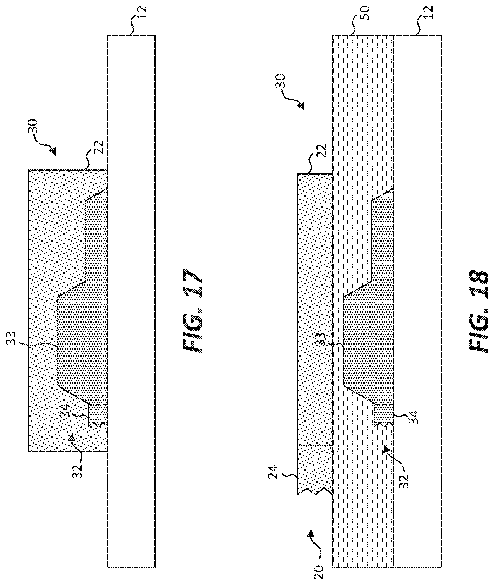
D00019

D00020

D00021

D00022

XML
uspto.report is an independent third-party trademark research tool that is not affiliated, endorsed, or sponsored by the United States Patent and Trademark Office (USPTO) or any other governmental organization. The information provided by uspto.report is based on publicly available data at the time of writing and is intended for informational purposes only.
While we strive to provide accurate and up-to-date information, we do not guarantee the accuracy, completeness, reliability, or suitability of the information displayed on this site. The use of this site is at your own risk. Any reliance you place on such information is therefore strictly at your own risk.
All official trademark data, including owner information, should be verified by visiting the official USPTO website at www.uspto.gov. This site is not intended to replace professional legal advice and should not be used as a substitute for consulting with a legal professional who is knowledgeable about trademark law.