3D microdisplay device and structure
Or-Bach , et al.
U.S. patent number 10,679,977 [Application Number 15/920,499] was granted by the patent office on 2020-06-09 for 3d microdisplay device and structure. This patent grant is currently assigned to Monolithic 3D Inc.. The grantee listed for this patent is Monolithic 3D Inc.. Invention is credited to Zvi Or-Bach, Deepak C. Sekar.


View All Diagrams
| United States Patent | 10,679,977 |
| Or-Bach , et al. | June 9, 2020 |
3D microdisplay device and structure
Abstract
A 3D micro display, the micro display including: a first single crystal layer including at least one LED driving circuit; and a second single crystal layer including a plurality of light emitting diodes (LEDs), where the second single crystal layer overlays the first single crystal layer, where the second single crystal layer includes at least ten first LED pixels, and where the second single crystal layer and the first single crystal layer are separated by a vertical distance of less than ten microns.
| Inventors: | Or-Bach; Zvi (San Jose, CA), Sekar; Deepak C. (San Jose, CA) | ||||||||||
|---|---|---|---|---|---|---|---|---|---|---|---|
| Applicant: |
|
||||||||||
| Assignee: | Monolithic 3D Inc. (San Jose,
CA) |
||||||||||
| Family ID: | 62841498 | ||||||||||
| Appl. No.: | 15/920,499 | ||||||||||
| Filed: | March 14, 2018 |
Prior Publication Data
| Document Identifier | Publication Date | |
|---|---|---|
| US 20180204826 A1 | Jul 19, 2018 | |
Related U.S. Patent Documents
| Application Number | Filing Date | Patent Number | Issue Date | ||
|---|---|---|---|---|---|
| 14936657 | Nov 9, 2015 | 9941319 | |||
| 13274161 | Oct 14, 2011 | 9197804 | |||
| 15920499 | |||||
| 12904103 | Oct 13, 2010 | 8163581 | |||
| Current U.S. Class: | 1/1 |
| Current CPC Class: | H01L 25/167 (20130101); H01L 21/845 (20130101); H01L 21/76283 (20130101); H01L 27/14603 (20130101); H01L 21/76254 (20130101); H01L 24/32 (20130101); H01L 25/0756 (20130101); H01L 27/1218 (20130101); H01L 33/382 (20130101); H01L 24/16 (20130101); H01L 21/823878 (20130101); H01L 24/83 (20130101); H01L 21/76275 (20130101); H01L 27/281 (20130101); H01L 33/0066 (20130101); H01L 33/06 (20130101); H01L 27/1211 (20130101); H01L 2224/32146 (20130101); H01L 33/32 (20130101); H01L 27/153 (20130101); H01L 2224/83896 (20130101); H01L 2224/29188 (20130101); H01L 2924/1426 (20130101); H01L 33/30 (20130101); H01L 2924/12041 (20130101); H01L 2224/16146 (20130101) |
| Current International Class: | H01L 27/146 (20060101); H01L 25/16 (20060101); H01L 21/762 (20060101); H01L 27/28 (20060101); H01L 27/12 (20060101); H01L 25/075 (20060101); H01L 33/38 (20100101); H01L 21/84 (20060101); H01L 21/8238 (20060101); H01L 23/00 (20060101); H01L 27/15 (20060101); H01L 33/30 (20100101); H01L 33/32 (20100101); H01L 33/06 (20100101); H01L 33/00 (20100101) |
References Cited [Referenced By]
U.S. Patent Documents
| 3007090 | October 1961 | Rutz |
| 3819959 | June 1974 | Chang et al. |
| 4009483 | February 1977 | Clark |
| 4197555 | April 1980 | Uehara et al. |
| 4213139 | July 1980 | Rao et al. |
| 4400715 | August 1983 | Barbee et al. |
| 4487635 | December 1984 | Kugimiya et al. |
| 4510670 | April 1985 | Schwabe |
| 4522657 | June 1985 | Rohatgi et al. |
| 4612083 | September 1986 | Yasumoto et al. |
| 4643950 | February 1987 | Ogura et al. |
| 4704785 | November 1987 | Curran |
| 4711858 | December 1987 | Harder et al. |
| 4721885 | January 1988 | Brodie |
| 4732312 | March 1988 | Kennedy et al. |
| 4733288 | March 1988 | Sato |
| 4829018 | May 1989 | Wahlstrom |
| 4854986 | August 1989 | Raby |
| 4866304 | September 1989 | Yu |
| 4939568 | July 1990 | Kato et al. |
| 4956307 | September 1990 | Pollack et al. |
| 5012153 | April 1991 | Atkinson et al. |
| 5032007 | July 1991 | Silverstein et al. |
| 5047979 | September 1991 | Leung |
| 5087585 | February 1992 | Hayashi |
| 5093704 | March 1992 | Sato et al. |
| 5106775 | April 1992 | Kaga et al. |
| 5152857 | October 1992 | Ito et al. |
| 5162879 | November 1992 | Gill |
| 5189500 | February 1993 | Kusunoki |
| 5217916 | June 1993 | Anderson et al. |
| 5250460 | October 1993 | Yamagata et al. |
| 5258643 | November 1993 | Cohen |
| 5265047 | November 1993 | Leung et al. |
| 5266511 | November 1993 | Takao |
| 5277748 | January 1994 | Sakaguchi et al. |
| 5286670 | February 1994 | Kang et al. |
| 5294556 | March 1994 | Kawamura |
| 5308782 | May 1994 | Mazure et al. |
| 5312771 | May 1994 | Yonehara |
| 5317236 | May 1994 | Zavracky et al. |
| 5324980 | June 1994 | Kusunoki |
| 5355022 | October 1994 | Sugahara et al. |
| 5371037 | December 1994 | Yonehara |
| 5374564 | December 1994 | Bruel |
| 5374581 | December 1994 | Ichikawa et al. |
| 5424560 | June 1995 | Norman et al. |
| 5475280 | December 1995 | Jones et al. |
| 5478762 | December 1995 | Chao |
| 5485031 | January 1996 | Zhang et al. |
| 5498978 | March 1996 | Takahashi et al. |
| 5527423 | June 1996 | Neville et al. |
| 5535342 | July 1996 | Taylor |
| 5554870 | September 1996 | Fitch et al. |
| 5563084 | October 1996 | Ramm et al. |
| 5583349 | December 1996 | Norman et al. |
| 5583350 | December 1996 | Norman et al. |
| 5586291 | December 1996 | Lasker |
| 5594563 | January 1997 | Larson |
| 5604137 | February 1997 | Yamazaki et al. |
| 5617991 | April 1997 | Pramanick et al. |
| 5627106 | May 1997 | Hsu |
| 5656548 | August 1997 | Zavracky et al. |
| 5656553 | August 1997 | Leas et al. |
| 5659194 | August 1997 | Iwamatsu |
| 5670411 | September 1997 | Yonehara |
| 5681756 | October 1997 | Norman et al. |
| 5695557 | December 1997 | Yamagata et al. |
| 5701027 | December 1997 | Gordon et al. |
| 5707745 | January 1998 | Forrest et al. |
| 5714395 | February 1998 | Bruel |
| 5721160 | February 1998 | Forrest et al. |
| 5737748 | April 1998 | Shigeeda |
| 5739552 | April 1998 | Kimura et al. |
| 5744979 | April 1998 | Goetting |
| 5748161 | May 1998 | Lebby et al. |
| 5757026 | May 1998 | Forrest et al. |
| 5770483 | June 1998 | Kadosh |
| 5770881 | June 1998 | Pelella et al. |
| 5781031 | July 1998 | Bertin et al. |
| 5817574 | October 1998 | Gardner |
| 5829026 | October 1998 | Leung et al. |
| 5835396 | November 1998 | Zhang |
| 5854123 | December 1998 | Sato et al. |
| 5861929 | January 1999 | Spitzer |
| 5877034 | March 1999 | Ramm |
| 5877070 | March 1999 | Goesele et al. |
| 5882987 | March 1999 | Srikrishnan |
| 5883525 | March 1999 | Tavana et al. |
| 5889903 | March 1999 | Rao |
| 5893721 | April 1999 | Huang et al. |
| 5915167 | June 1999 | Leedy |
| 5920788 | July 1999 | Reinberg |
| 5937312 | August 1999 | Iyer et al. |
| 5943574 | August 1999 | Tehrani et al. |
| 5952680 | September 1999 | Strite |
| 5952681 | September 1999 | Chen |
| 5965875 | October 1999 | Merrill |
| 5977579 | November 1999 | Noble |
| 5977961 | November 1999 | Rindal |
| 5980633 | November 1999 | Yamagata et al. |
| 5985742 | November 1999 | Henley et al. |
| 5994746 | November 1999 | Reisinger |
| 5998808 | December 1999 | Matsushita |
| 6001693 | December 1999 | Yeouchung et al. |
| 6009496 | December 1999 | Tsai |
| 6020252 | February 2000 | Aspar et al. |
| 6020263 | February 2000 | Shih et al. |
| 6027958 | February 2000 | Vu et al. |
| 6030700 | February 2000 | Forrest et al. |
| 6052498 | April 2000 | Paniccia |
| 6054370 | April 2000 | Doyle |
| 6057212 | May 2000 | Chan et al. |
| 6071795 | June 2000 | Cheung et al. |
| 6075268 | June 2000 | Gardner et al. |
| 6103597 | August 2000 | Aspar et al. |
| 6111260 | August 2000 | Dawson et al. |
| 6125217 | September 2000 | Paniccia et al. |
| 6153495 | November 2000 | Kub et al. |
| 6191007 | February 2001 | Matsui et al. |
| 6200878 | March 2001 | Yamagata |
| 6222203 | April 2001 | Ishibashi et al. |
| 6226197 | May 2001 | Nishimura |
| 6229161 | May 2001 | Nemati et al. |
| 6242324 | June 2001 | Kub et al. |
| 6242778 | June 2001 | Marmillion et al. |
| 6252465 | June 2001 | Katoh |
| 6259623 | July 2001 | Takahashi |
| 6261935 | July 2001 | See et al. |
| 6264805 | July 2001 | Forrest et al. |
| 6281102 | August 2001 | Cao et al. |
| 6294018 | September 2001 | Hamm et al. |
| 6306705 | October 2001 | Parekh et al. |
| 6321134 | November 2001 | Henley et al. |
| 6322903 | November 2001 | Siniaguine et al. |
| 6331468 | December 2001 | Aronowitz et al. |
| 6331790 | December 2001 | Or-Bach et al. |
| 6331943 | December 2001 | Naji et al. |
| 6353492 | March 2002 | McClelland et al. |
| 6355501 | March 2002 | Fung et al. |
| 6355976 | March 2002 | Faris |
| 6358631 | March 2002 | Forrest et al. |
| 6365270 | April 2002 | Forrest et al. |
| 6376337 | April 2002 | Wang et al. |
| 6377504 | April 2002 | Hilbert |
| 6380046 | April 2002 | Yamazaki |
| 6392253 | May 2002 | Saxena |
| 6404043 | June 2002 | Isaak |
| 6417108 | July 2002 | Akino et al. |
| 6420215 | July 2002 | Knall et al. |
| 6423614 | July 2002 | Doyle |
| 6429481 | August 2002 | Mo et al. |
| 6429484 | August 2002 | Yu |
| 6430734 | August 2002 | Zahar |
| 6448615 | September 2002 | Forbes |
| 6475869 | November 2002 | Yu |
| 6476493 | November 2002 | Or-Bach et al. |
| 6479821 | November 2002 | Hawryluk et al. |
| 6483707 | November 2002 | Freuler et al. |
| 6507115 | January 2003 | Hofstee |
| 6515334 | February 2003 | Yamazaki et al. |
| 6515511 | February 2003 | Sugibayashi et al. |
| 6526559 | February 2003 | Schiefele et al. |
| 6528391 | March 2003 | Henley et al. |
| 6534352 | March 2003 | Kim |
| 6534382 | March 2003 | Sakaguchi et al. |
| 6544837 | April 2003 | Divakauni et al. |
| 6545314 | April 2003 | Forbes et al. |
| 6555901 | April 2003 | Yoshihara et al. |
| 6563139 | May 2003 | Hen |
| 6580124 | June 2003 | Cleeves |
| 6580289 | June 2003 | Cox |
| 6600173 | July 2003 | Tiwari |
| 6617694 | September 2003 | Kodaira et al. |
| 6620659 | September 2003 | Emmma et al. |
| 6624046 | September 2003 | Zavracky et al. |
| 6627518 | September 2003 | Inoue et al. |
| 6627985 | September 2003 | Huppenthal et al. |
| 6630713 | October 2003 | Geusic |
| 6635552 | October 2003 | Gonzalez |
| 6635588 | October 2003 | Hawryluk et al. |
| 6638834 | October 2003 | Gonzalez |
| 6642744 | November 2003 | Or-Bach et al. |
| 6653209 | November 2003 | Yamagata |
| 6653712 | November 2003 | Knall et al. |
| 6661085 | December 2003 | Kellar et al. |
| 6677204 | January 2004 | Cleeves et al. |
| 6686253 | February 2004 | Or-Bach |
| 6689660 | February 2004 | Noble |
| 6701071 | March 2004 | Wada et al. |
| 6703328 | March 2004 | Tanaka et al. |
| 6756633 | June 2004 | Wang et al. |
| 6756811 | June 2004 | Or-Bach |
| 6759282 | July 2004 | Campbell et al. |
| 6762076 | July 2004 | Kim et al. |
| 6774010 | August 2004 | Chu et al. |
| 6805979 | October 2004 | Ogura et al. |
| 6806171 | October 2004 | Ulyashin et al. |
| 6809009 | October 2004 | Aspar et al. |
| 6815781 | November 2004 | Vyvoda et al. |
| 6819136 | November 2004 | Or-Bach |
| 6821826 | November 2004 | Chan et al. |
| 6841813 | January 2005 | Walker et al. |
| 6844243 | January 2005 | Gonzalez |
| 6864534 | March 2005 | Ipposhi et al. |
| 6875671 | April 2005 | Faris |
| 6882572 | April 2005 | Wang et al. |
| 6888375 | May 2005 | Feng et al. |
| 6917219 | July 2005 | New |
| 6927431 | August 2005 | Gonzalez |
| 6930511 | August 2005 | Or-Bach |
| 6943067 | September 2005 | Greenlaw |
| 6943407 | September 2005 | Ouyang et al. |
| 6949421 | September 2005 | Padmanabhan et al. |
| 6953956 | October 2005 | Or-Bach et al. |
| 6967149 | November 2005 | Meyer et al. |
| 6985012 | January 2006 | Or-Bach |
| 6989687 | January 2006 | Or-Bach |
| 6995430 | February 2006 | Langdo et al. |
| 6995456 | February 2006 | Nowak |
| 7015719 | March 2006 | Feng et al. |
| 7016569 | March 2006 | Mule et al. |
| 7018875 | March 2006 | Madurawe |
| 7019557 | March 2006 | Madurawe |
| 7043106 | May 2006 | West et al. |
| 7052941 | May 2006 | Lee |
| 7064579 | June 2006 | Madurawe |
| 7067396 | June 2006 | Aspar et al. |
| 7067909 | June 2006 | Reif et al. |
| 7068070 | June 2006 | Or-Bach |
| 7068072 | June 2006 | New et al. |
| 7078739 | July 2006 | Nemati et al. |
| 7094667 | August 2006 | Bower |
| 7098691 | August 2006 | Or-Bach et al. |
| 7105390 | September 2006 | Brask et al. |
| 7105871 | September 2006 | Or-Bach et al. |
| 7109092 | September 2006 | Tong |
| 7110629 | September 2006 | Bjorkman et al. |
| 7111149 | September 2006 | Eilert |
| 7112815 | September 2006 | Prall |
| 7115945 | October 2006 | Lee et al. |
| 7115966 | October 2006 | Ido et al. |
| 7141853 | November 2006 | Campbell et al. |
| 7148119 | December 2006 | Sakaguchi et al. |
| 7157787 | January 2007 | Kim et al. |
| 7157937 | January 2007 | Apostol et al. |
| 7166520 | January 2007 | Henley |
| 7170807 | January 2007 | Fazan et al. |
| 7173369 | February 2007 | Forrest et al. |
| 7180091 | February 2007 | Yamazaki et al. |
| 7180379 | February 2007 | Hopper et al. |
| 7183611 | February 2007 | Bhattacharyya |
| 7189489 | March 2007 | Kunimoto et al. |
| 7205204 | April 2007 | Ogawa et al. |
| 7209384 | April 2007 | Kim |
| 7217636 | May 2007 | Atanackovic |
| 7223612 | May 2007 | Sarma |
| 7242012 | July 2007 | Leedy |
| 7245002 | July 2007 | Akino et al. |
| 7256104 | August 2007 | Ito et al. |
| 7259091 | August 2007 | Schuehrer et al. |
| 7265421 | September 2007 | Madurawe |
| 7271420 | September 2007 | Cao |
| 7274207 | September 2007 | Sugawara et al. |
| 7282951 | October 2007 | Huppenthal et al. |
| 7284226 | October 2007 | Kondapalli |
| 7296201 | November 2007 | Abramovici |
| 7304355 | December 2007 | Zhang |
| 7312109 | December 2007 | Madurawe |
| 7312487 | December 2007 | Alam et al. |
| 7314788 | January 2008 | Shaw |
| 7335573 | February 2008 | Takayama et al. |
| 7337425 | February 2008 | Kirk |
| 7338884 | March 2008 | Shimoto et al. |
| 7342415 | March 2008 | Teig et al. |
| 7351644 | April 2008 | Henley |
| 7358601 | April 2008 | Plants et al. |
| 7362133 | April 2008 | Madurawe |
| 7369435 | May 2008 | Forbes |
| 7371660 | May 2008 | Henley et al. |
| 7378702 | May 2008 | Lee |
| 7381989 | June 2008 | Kim |
| 7385283 | June 2008 | Wu |
| 7393722 | July 2008 | Issaq et al. |
| 7402483 | July 2008 | Yu et al. |
| 7402897 | July 2008 | Leedy |
| 7419844 | September 2008 | Lee et al. |
| 7432185 | October 2008 | Kim |
| 7436027 | October 2008 | Ogawa et al. |
| 7439773 | October 2008 | Or-Bach et al. |
| 7446563 | November 2008 | Madurawe |
| 7459752 | December 2008 | Doris et al. |
| 7459763 | December 2008 | Issaq et al. |
| 7459772 | December 2008 | Speers |
| 7463062 | December 2008 | Or-Bach et al. |
| 7463502 | December 2008 | Stipe |
| 7470142 | December 2008 | Lee |
| 7470598 | December 2008 | Lee |
| 7476939 | January 2009 | Okhonin et al. |
| 7477540 | January 2009 | Okhonin et al. |
| 7485968 | February 2009 | Enquist et al. |
| 7486563 | February 2009 | Waller et al. |
| 7488980 | February 2009 | Takafuji et al. |
| 7492632 | February 2009 | Carman |
| 7495473 | February 2009 | McCollum et al. |
| 7498675 | March 2009 | Farnworth et al. |
| 7499352 | March 2009 | Singh |
| 7499358 | March 2009 | Bauser |
| 7508034 | March 2009 | Takafuji et al. |
| 7514748 | April 2009 | Fazan et al. |
| 7521806 | April 2009 | Trezza |
| 7525186 | April 2009 | Kim et al. |
| 7535089 | May 2009 | Fitzgerald |
| 7541616 | June 2009 | Fazan et al. |
| 7547589 | June 2009 | Iriguchi |
| 7553745 | June 2009 | Lim |
| 7557367 | July 2009 | Rogers et al. |
| 7558141 | July 2009 | Katsumata et al. |
| 7563659 | July 2009 | Kwon et al. |
| 7566855 | July 2009 | Olsen et al. |
| 7566974 | July 2009 | Konevecki |
| 7586778 | September 2009 | Ho et al. |
| 7589375 | September 2009 | Jang et al. |
| 7608848 | October 2009 | Ho et al. |
| 7612411 | November 2009 | Walker |
| 7622367 | November 2009 | Nuzzo et al. |
| 7632738 | December 2009 | Lee |
| 7633162 | December 2009 | Lee |
| 7666723 | February 2010 | Frank et al. |
| 7671371 | March 2010 | Lee |
| 7671460 | March 2010 | Lauxtermann et al. |
| 7674687 | March 2010 | Henley |
| 7687372 | March 2010 | Jain |
| 7687872 | March 2010 | Cazaux |
| 7688619 | March 2010 | Lung et al. |
| 7692202 | April 2010 | Bensch |
| 7692448 | April 2010 | Solomon |
| 7692944 | April 2010 | Bernstein et al. |
| 7697316 | April 2010 | Lai et al. |
| 7709932 | May 2010 | Nemoto et al. |
| 7718508 | May 2010 | Lee |
| 7719876 | May 2010 | Chevallier |
| 7723207 | May 2010 | Alam et al. |
| 7728326 | June 2010 | Yamazaki et al. |
| 7732301 | June 2010 | Pinnington et al. |
| 7741673 | June 2010 | Tak et al. |
| 7742331 | June 2010 | Watanabe |
| 7745250 | June 2010 | Han |
| 7749884 | July 2010 | Mathew et al. |
| 7750669 | July 2010 | Spangaro |
| 7755622 | July 2010 | Yvon |
| 7759043 | July 2010 | Tanabe et al. |
| 7768115 | August 2010 | Lee et al. |
| 7772039 | August 2010 | Kerber |
| 7772096 | August 2010 | DeSouza et al. |
| 7774735 | August 2010 | Sood |
| 7776715 | August 2010 | Wells et al. |
| 7777330 | August 2010 | Pelley et al. |
| 7786460 | August 2010 | Lung et al. |
| 7786535 | August 2010 | Abou-Khalil et al. |
| 7790524 | September 2010 | Abadeer et al. |
| 7795619 | September 2010 | Hara |
| 7799675 | September 2010 | Lee |
| 7800099 | September 2010 | Yamazaki et al. |
| 7800148 | September 2010 | Lee et al. |
| 7800163 | September 2010 | Izumi et al. |
| 7800199 | September 2010 | Oh et al. |
| 7816721 | October 2010 | Yamazaki |
| 7843718 | November 2010 | Koh et al. |
| 7846814 | December 2010 | Lee |
| 7863095 | January 2011 | Sasaki et al. |
| 7864568 | January 2011 | Fujisaki et al. |
| 7867822 | January 2011 | Lee |
| 7888764 | February 2011 | Lee |
| 7910432 | March 2011 | Tanaka et al. |
| 7915164 | March 2011 | Konevecki et al. |
| 7919845 | April 2011 | Karp |
| 7965102 | June 2011 | Bauer et al. |
| 7968965 | June 2011 | Kim |
| 7969193 | June 2011 | Wu et al. |
| 7973314 | July 2011 | Yang |
| 7982250 | July 2011 | Yamazaki et al. |
| 8008732 | August 2011 | Kiyotoshi |
| 8013399 | September 2011 | Thomas et al. |
| 8014166 | September 2011 | Yazdani |
| 8014195 | September 2011 | Okhonin et al. |
| 8022493 | September 2011 | Bang |
| 8030780 | October 2011 | Kirby et al. |
| 8031544 | October 2011 | Kim et al. |
| 8032857 | October 2011 | McIlrath |
| 8044448 | October 2011 | Kamigaichi et al. |
| 8044464 | October 2011 | Yamazaki et al. |
| 8068364 | November 2011 | Maejima |
| 8106520 | January 2012 | Keeth et al. |
| 8107276 | January 2012 | Breitwisch et al. |
| 8129256 | March 2012 | Farooq et al. |
| 8129258 | March 2012 | Hosier et al. |
| 8130547 | March 2012 | Widjaja et al. |
| 8136071 | March 2012 | Solomon |
| 8138502 | March 2012 | Nakamura et al. |
| 8153520 | April 2012 | Chandrashekar |
| 8158515 | April 2012 | Farooq et al. |
| 8178919 | May 2012 | Fujiwara et al. |
| 8183630 | May 2012 | Batude et al. |
| 8184463 | May 2012 | Saen et al. |
| 8185685 | May 2012 | Selinger |
| 8203187 | June 2012 | Lung et al. |
| 8208279 | June 2012 | Lue |
| 8209649 | June 2012 | McIlrath |
| 8228684 | July 2012 | Losavio et al. |
| 8266560 | August 2012 | McIlrath |
| 8264065 | September 2012 | Su et al. |
| 8288816 | October 2012 | Komori et al. |
| 8294199 | October 2012 | Yahashi et al. |
| 8324680 | December 2012 | Izumi et al. |
| 8338882 | December 2012 | Tanaka et al. |
| 8343851 | January 2013 | Kim et al. |
| 8354308 | January 2013 | Kang et al. |
| 8355273 | January 2013 | Liu |
| 8374033 | February 2013 | Kito et al. |
| 8432719 | April 2013 | Lue |
| 8432751 | April 2013 | Hafez |
| 8455941 | June 2013 | Ishihara et al. |
| 8470689 | June 2013 | Desplobain et al. |
| 8497512 | July 2013 | Nakamura et al. |
| 8501564 | August 2013 | Suzawa |
| 8507972 | August 2013 | Oota et al. |
| 8508994 | August 2013 | Okhonin |
| 8513725 | August 2013 | Sakuma et al. |
| 8514623 | August 2013 | Widjaja et al. |
| 8566762 | August 2013 | Morimoto et al. |
| 8525342 | October 2013 | Chandrasekaran |
| 8546956 | October 2013 | Nguyen |
| 8603888 | December 2013 | Liu |
| 8619490 | December 2013 | Yu |
| 8643162 | February 2014 | Madurawe |
| 8650516 | February 2014 | McIlrath |
| 8679861 | March 2014 | Bose |
| 8773562 | July 2014 | Fan |
| 8775998 | July 2014 | Morimoto |
| 8841777 | September 2014 | Farooq |
| 8853785 | October 2014 | Augendre |
| 8896054 | November 2014 | Sakuma et al. |
| 8928119 | January 2015 | Leedy |
| 8971114 | March 2015 | Kang |
| 9172008 | October 2015 | Hwang |
| 9227456 | January 2016 | Chien |
| 9230973 | January 2016 | Pachamuthu et al. |
| 9334582 | May 2016 | See |
| 9564450 | February 2017 | Sakuma et al. |
| 9570683 | February 2017 | Jo |
| 9589982 | March 2017 | Cheng et al. |
| 9595530 | March 2017 | Zhou |
| 9673257 | June 2017 | Takaki |
| 9997530 | June 2018 | Yon et al. |
| 2001/0000005 | March 2001 | Forrest et al. |
| 2001/0014391 | August 2001 | Forrest et al. |
| 2001/0028059 | October 2001 | Emma et al. |
| 2002/0024140 | February 2002 | Nakajima et al. |
| 2002/0025604 | February 2002 | Tiwari |
| 2002/0074668 | June 2002 | Hofstee et al. |
| 2002/0081823 | June 2002 | Cheung et al. |
| 2002/0090758 | July 2002 | Henley et al. |
| 2002/0096681 | July 2002 | Yamazaki et al. |
| 2002/0113289 | August 2002 | Cordes et al. |
| 2002/0132465 | September 2002 | Leedy |
| 2002/0140091 | October 2002 | Callahan |
| 2002/0141233 | October 2002 | Hosotani et al. |
| 2002/0153243 | October 2002 | Forrest et al. |
| 2002/0153569 | October 2002 | Katayama |
| 2002/0175401 | November 2002 | Huang et al. |
| 2002/0180069 | December 2002 | Houston |
| 2002/0190232 | December 2002 | Chason |
| 2002/0199110 | December 2002 | Kean |
| 2003/0015713 | January 2003 | Yoo |
| 2003/0032262 | February 2003 | Dennison et al. |
| 2003/0059999 | March 2003 | Gonzalez |
| 2003/0060034 | March 2003 | Beyne et al. |
| 2003/0061555 | March 2003 | Kamei |
| 2003/0067043 | April 2003 | Zhang |
| 2003/0076706 | April 2003 | Andoh |
| 2003/0102079 | June 2003 | Kalvesten et al. |
| 2003/0107117 | June 2003 | Antonelli et al. |
| 2003/0113963 | June 2003 | Wurzer |
| 2003/0119279 | June 2003 | Enquist |
| 2003/0139011 | July 2003 | Cleeves et al. |
| 2003/0153163 | August 2003 | Letertre |
| 2003/0157748 | August 2003 | Kim et al. |
| 2003/0160888 | August 2003 | Yoshikawa |
| 2003/0173631 | September 2003 | Murakami |
| 2003/0206036 | November 2003 | Or-Bach |
| 2003/0213967 | November 2003 | Forrest et al. |
| 2003/0224582 | December 2003 | Shimoda et al. |
| 2003/0224596 | December 2003 | Marxsen et al. |
| 2004/0007376 | January 2004 | Urdahl et al. |
| 2004/0014299 | January 2004 | Moriceau et al. |
| 2004/0033676 | February 2004 | Coronel et al. |
| 2004/0036126 | February 2004 | Chau et al. |
| 2004/0047539 | March 2004 | Okubora et al. |
| 2004/0061176 | April 2004 | Takafuji et al. |
| 2004/0113207 | June 2004 | Hsu et al. |
| 2004/0143797 | July 2004 | Nguyen |
| 2004/0150068 | August 2004 | Leedy |
| 2004/0150070 | August 2004 | Okada |
| 2004/0152272 | August 2004 | Fladre et al. |
| 2004/0155301 | August 2004 | Zhang |
| 2004/0156172 | August 2004 | Lin et al. |
| 2004/0156233 | August 2004 | Bhattacharyya |
| 2004/0164425 | August 2004 | Urakawa |
| 2004/0166649 | August 2004 | Bressot et al. |
| 2004/0174732 | September 2004 | Morimoto |
| 2004/0175902 | September 2004 | Rayssac et al. |
| 2004/0178819 | September 2004 | New |
| 2004/0195572 | October 2004 | Kato et al. |
| 2004/0219765 | November 2004 | Reif et al. |
| 2004/0229444 | November 2004 | Couillard |
| 2004/0259312 | December 2004 | Schlosser et al. |
| 2004/0262635 | December 2004 | Lee |
| 2004/0262772 | December 2004 | Ramanathan et al. |
| 2005/0003592 | January 2005 | Jones |
| 2005/0010725 | January 2005 | Eilert |
| 2005/0023656 | February 2005 | Leedy |
| 2005/0045919 | March 2005 | Kaeriyama et al. |
| 2005/0067620 | March 2005 | Chan et al. |
| 2005/0067625 | March 2005 | Hata |
| 2005/0073060 | April 2005 | Datta et al. |
| 2005/0082526 | April 2005 | Bedell et al. |
| 2005/0098822 | May 2005 | Mathew |
| 2005/0110041 | May 2005 | Boutros et al. |
| 2005/0121676 | June 2005 | Fried et al. |
| 2005/0121789 | June 2005 | Madurawe |
| 2005/0130351 | June 2005 | Leedy |
| 2005/0130429 | June 2005 | Rayssac et al. |
| 2005/0148137 | July 2005 | Brask et al. |
| 2005/0176174 | August 2005 | Leedy |
| 2005/0218521 | October 2005 | Lee |
| 2005/0225237 | October 2005 | Winters |
| 2005/0266659 | December 2005 | Ghyselen et al. |
| 2005/0273749 | December 2005 | Kirk |
| 2005/0280061 | December 2005 | Lee |
| 2005/0280090 | December 2005 | Anderson et al. |
| 2005/0280154 | December 2005 | Lee |
| 2005/0280155 | December 2005 | Lee |
| 2005/0280156 | December 2005 | Lee |
| 2005/0282019 | December 2005 | Fukushima et al. |
| 2006/0014331 | January 2006 | Tang et al. |
| 2006/0024923 | February 2006 | Sarma et al. |
| 2006/0033110 | February 2006 | Alam et al. |
| 2006/0033124 | February 2006 | Or-Bach et al. |
| 2006/0043367 | February 2006 | Chang et al. |
| 2006/0049449 | March 2006 | Iino |
| 2006/0065953 | March 2006 | Kim et al. |
| 2006/0067122 | March 2006 | Verhoeven |
| 2006/0071322 | April 2006 | Kitamura |
| 2006/0071332 | April 2006 | Speers |
| 2006/0083280 | April 2006 | Tauzin et al. |
| 2006/0108613 | May 2006 | Song |
| 2006/0113522 | June 2006 | Lee et al. |
| 2006/0118935 | June 2006 | Kamiyama et al. |
| 2006/0121690 | June 2006 | Pogge et al. |
| 2006/0150137 | July 2006 | Madurawe |
| 2006/0158511 | July 2006 | Harrold |
| 2006/0170046 | August 2006 | Hara |
| 2006/0179417 | August 2006 | Madurawe |
| 2006/0181202 | August 2006 | Liao et al. |
| 2006/0189095 | August 2006 | Ghyselen et al. |
| 2006/0194401 | August 2006 | Hu et al. |
| 2006/0195729 | August 2006 | Huppenthal et al. |
| 2006/0207087 | September 2006 | Jafri et al. |
| 2006/0224814 | October 2006 | Kim et al. |
| 2006/0237777 | October 2006 | Choi |
| 2006/0249859 | November 2006 | Eiles et al. |
| 2006/0275962 | December 2006 | Lee |
| 2007/0004150 | January 2007 | Huang |
| 2007/0014508 | January 2007 | Chen et al. |
| 2007/0035329 | February 2007 | Madurawe |
| 2007/0063259 | March 2007 | Derderian et al. |
| 2007/0072391 | March 2007 | Pocas et al. |
| 2007/0076509 | April 2007 | Zhang |
| 2007/0077694 | April 2007 | Lee |
| 2007/0077743 | April 2007 | Rao et al. |
| 2007/0090416 | April 2007 | Doyle et al. |
| 2007/0102737 | May 2007 | Kashiwabara et al. |
| 2007/0103191 | May 2007 | Sugawara et al. |
| 2007/0108523 | May 2007 | Ogawa et al. |
| 2007/0109831 | May 2007 | RaghuRam |
| 2007/0111386 | May 2007 | Kim et al. |
| 2007/0111406 | May 2007 | Joshi et al. |
| 2007/0132049 | June 2007 | Stipe |
| 2007/0132369 | June 2007 | Forrest et al. |
| 2007/0135013 | June 2007 | Faris |
| 2007/0141781 | June 2007 | Park |
| 2007/0158659 | July 2007 | Bensce |
| 2007/0158831 | July 2007 | Cha et al. |
| 2007/0187775 | August 2007 | Okhonin et al. |
| 2007/0190746 | August 2007 | Ito et al. |
| 2007/0194453 | August 2007 | Chakraborty et al. |
| 2007/0206408 | September 2007 | Schwerin |
| 2007/0210336 | September 2007 | Madurawe |
| 2007/0211535 | September 2007 | Kim |
| 2007/0215903 | September 2007 | Sakamoto et al. |
| 2007/0218622 | September 2007 | Lee et al. |
| 2007/0228383 | October 2007 | Bernstein et al. |
| 2007/0252201 | November 2007 | Kito et al. |
| 2007/0252203 | November 2007 | Zhu et al. |
| 2007/0262457 | November 2007 | Lin |
| 2007/0275520 | November 2007 | Suzuki |
| 2007/0281439 | December 2007 | Bedell et al. |
| 2007/0283298 | December 2007 | Bernstein et al. |
| 2007/0287224 | December 2007 | Alam et al. |
| 2007/0296073 | December 2007 | Wu |
| 2007/0297232 | December 2007 | Iwata |
| 2008/0001204 | January 2008 | Lee |
| 2008/0003818 | January 2008 | Seidel et al. |
| 2008/0030228 | February 2008 | Amarilio |
| 2008/0032463 | February 2008 | Lee |
| 2008/0038902 | February 2008 | Lee |
| 2008/0048239 | February 2008 | Huo |
| 2008/0048327 | February 2008 | Lee |
| 2008/0054359 | March 2008 | Yang et al. |
| 2008/0067573 | March 2008 | Jang et al. |
| 2008/0070340 | March 2008 | Borrelli et al. |
| 2008/0072182 | March 2008 | He et al. |
| 2008/0099780 | May 2008 | Tran |
| 2008/0099819 | May 2008 | Kito et al. |
| 2008/0108171 | May 2008 | Rogers et al. |
| 2008/0124845 | May 2008 | Yu et al. |
| 2008/0128745 | June 2008 | Mastro et al. |
| 2008/0128780 | June 2008 | Nishihara |
| 2008/0135949 | June 2008 | Lo et al. |
| 2008/0136455 | June 2008 | Diamant et al. |
| 2008/0142937 | June 2008 | Chen et al. |
| 2008/0142959 | June 2008 | DeMulder et al. |
| 2008/0143379 | June 2008 | Norman |
| 2008/0150579 | June 2008 | Madurawe |
| 2008/0160431 | July 2008 | Scott et al. |
| 2008/0160726 | July 2008 | Lim et al. |
| 2008/0165521 | July 2008 | Bernstein et al. |
| 2008/0175032 | July 2008 | Tanaka et al. |
| 2008/0179678 | July 2008 | Dyer et al. |
| 2008/0180132 | July 2008 | Ishikawa |
| 2008/0185648 | August 2008 | Jeong |
| 2008/0191247 | August 2008 | Yin et al. |
| 2008/0191312 | August 2008 | Oh et al. |
| 2008/0194068 | August 2008 | Temmler et al. |
| 2008/0203452 | August 2008 | Moon et al. |
| 2008/0213982 | September 2008 | Park et al. |
| 2008/0220558 | September 2008 | Zehavi et al. |
| 2008/0220565 | September 2008 | Hsu et al. |
| 2008/0224260 | September 2008 | Schmit et al. |
| 2008/0237591 | October 2008 | Leedy |
| 2008/0239818 | October 2008 | Mokhlesi |
| 2008/0242028 | October 2008 | Mokhlesi |
| 2008/0248618 | October 2008 | Ahn et al. |
| 2008/0251862 | October 2008 | Fonash et al. |
| 2008/0254561 | October 2008 | Yoo |
| 2008/0254572 | October 2008 | Leedy |
| 2008/0254623 | October 2008 | Chan |
| 2008/0261378 | October 2008 | Yao et al. |
| 2008/0266960 | October 2008 | Kuo |
| 2008/0272492 | November 2008 | Tsang |
| 2008/0277778 | November 2008 | Furman et al. |
| 2008/0283873 | November 2008 | Yang |
| 2008/0283875 | November 2008 | Mukasa et al. |
| 2008/0284611 | November 2008 | Leedy |
| 2008/0296681 | December 2008 | Georgakos et al. |
| 2008/0315253 | December 2008 | Yuan |
| 2008/0315351 | December 2008 | Kakehata |
| 2009/0001469 | January 2009 | Yoshida et al. |
| 2009/0001504 | January 2009 | Takei et al. |
| 2009/0016716 | January 2009 | Ishida |
| 2009/0026541 | January 2009 | Chung |
| 2009/0026618 | January 2009 | Kim |
| 2009/0032899 | February 2009 | Irie |
| 2009/0032951 | February 2009 | Andry et al. |
| 2009/0039918 | February 2009 | Madurawe |
| 2009/0052827 | February 2009 | Durfee et al. |
| 2009/0055789 | February 2009 | McIlrath |
| 2009/0057879 | March 2009 | Garrou et al. |
| 2009/0061572 | March 2009 | Hareland et al. |
| 2009/0064058 | March 2009 | McIlrath |
| 2009/0065827 | March 2009 | Hwang |
| 2009/0066365 | March 2009 | Solomon |
| 2009/0066366 | March 2009 | Solomon |
| 2009/0070721 | March 2009 | Solomon |
| 2009/0070727 | March 2009 | Solomon |
| 2009/0078970 | March 2009 | Yamazaki |
| 2009/0079000 | March 2009 | Yamazaki et al. |
| 2009/0081848 | March 2009 | Erokhin |
| 2009/0087759 | April 2009 | Matsumoto et al. |
| 2009/0096009 | April 2009 | Dong et al. |
| 2009/0096024 | April 2009 | Shingu et al. |
| 2009/0108318 | April 2009 | Yoon et al. |
| 2009/0115042 | May 2009 | Koyanagi |
| 2009/0128189 | May 2009 | Madurawe et al. |
| 2009/0134397 | May 2009 | Yokoi et al. |
| 2009/0144669 | June 2009 | Bose et al. |
| 2009/0144678 | June 2009 | Bose et al. |
| 2009/0146172 | June 2009 | Pumyea |
| 2009/0159870 | June 2009 | Lin et al. |
| 2009/0160482 | June 2009 | Karp et al. |
| 2009/0161401 | June 2009 | Bigler et al. |
| 2009/0162993 | June 2009 | Yui et al. |
| 2009/0166627 | July 2009 | Han |
| 2009/0174018 | July 2009 | Dungan |
| 2009/0179268 | July 2009 | Abou-Khalil et al. |
| 2009/0185407 | July 2009 | Park |
| 2009/0194152 | August 2009 | Liu et al. |
| 2009/0194768 | August 2009 | Leedy |
| 2009/0194829 | August 2009 | Chung |
| 2009/0194836 | August 2009 | Kim |
| 2009/0204933 | August 2009 | Rezgui |
| 2009/0212317 | August 2009 | Kolodin et al. |
| 2009/0218627 | September 2009 | Zhu |
| 2009/0221110 | September 2009 | Lee et al. |
| 2009/0224330 | September 2009 | Hong |
| 2009/0224364 | September 2009 | Oh et al. |
| 2009/0230462 | September 2009 | Tanaka et al. |
| 2009/0234331 | September 2009 | Langereis et al. |
| 2009/0236749 | September 2009 | Otemba et al. |
| 2009/0242893 | October 2009 | Tomiyasu |
| 2009/0242935 | October 2009 | Fitzgerald |
| 2009/0250686 | October 2009 | Sato et al. |
| 2009/0262572 | October 2009 | Krusin-Elbaum |
| 2009/0262583 | October 2009 | Lue |
| 2009/0263942 | October 2009 | Ohnuma et al. |
| 2009/0267233 | October 2009 | Lee |
| 2009/0268983 | October 2009 | Stone et al. |
| 2009/0272989 | November 2009 | Shum et al. |
| 2009/0290434 | November 2009 | Kurjanowicz |
| 2009/0294822 | December 2009 | Batude et al. |
| 2009/0294836 | December 2009 | Kiyotoshi |
| 2009/0294861 | December 2009 | Thomas et al. |
| 2009/0302294 | December 2009 | Kim |
| 2009/0302387 | December 2009 | Joshi et al. |
| 2009/0302394 | December 2009 | Fujita |
| 2009/0309152 | December 2009 | Knoefler et al. |
| 2009/0315095 | December 2009 | Kim |
| 2009/0317950 | December 2009 | Okihara |
| 2009/0321830 | December 2009 | Maly |
| 2009/0321853 | December 2009 | Cheng |
| 2009/0321948 | December 2009 | Wang et al. |
| 2009/0325343 | December 2009 | Lee |
| 2010/0001282 | January 2010 | Mieno |
| 2010/0013049 | January 2010 | Tanaka |
| 2010/0025766 | February 2010 | Nuttinck et al. |
| 2010/0025825 | February 2010 | DeGraw et al. |
| 2010/0031217 | February 2010 | Sinha et al. |
| 2010/0032635 | February 2010 | Schwerin |
| 2010/0038699 | February 2010 | Katsumata et al. |
| 2010/0038743 | February 2010 | Lee |
| 2010/0045849 | February 2010 | Yamasaki |
| 2010/0052134 | March 2010 | Werner et al. |
| 2010/0058580 | March 2010 | Yazdani |
| 2010/0059796 | March 2010 | Scheuerlein |
| 2010/0078770 | April 2010 | Purushothaman et al. |
| 2010/0081232 | April 2010 | Furman et al. |
| 2010/0089627 | April 2010 | Huang et al. |
| 2010/0090188 | April 2010 | Fatasuyama |
| 2010/0112753 | May 2010 | Lee |
| 2010/0112810 | May 2010 | Lee et al. |
| 2010/0117048 | May 2010 | Lung et al. |
| 2010/0123202 | May 2010 | Hofmann |
| 2010/0123480 | May 2010 | Kitada et al. |
| 2010/0133695 | June 2010 | Lee |
| 2010/0133704 | June 2010 | Marimuthu et al. |
| 2010/0137143 | June 2010 | Rothberg et al. |
| 2010/0139836 | June 2010 | Horikoshi |
| 2010/0140790 | June 2010 | Setiadi et al. |
| 2010/0155932 | June 2010 | Gambino |
| 2010/0157117 | June 2010 | Wang |
| 2010/0159650 | June 2010 | Song |
| 2010/0181600 | July 2010 | Law |
| 2010/0190334 | July 2010 | Lee |
| 2010/0193884 | August 2010 | Park et al. |
| 2010/0193964 | August 2010 | Farooq et al. |
| 2010/0219392 | September 2010 | Awaya |
| 2010/0221867 | September 2010 | Bedell et al. |
| 2010/0224876 | September 2010 | Zhu |
| 2010/0224915 | September 2010 | Kawashima et al. |
| 2010/0225002 | September 2010 | Law et al. |
| 2010/0232200 | September 2010 | Shepard |
| 2010/0252934 | October 2010 | Law |
| 2010/0264551 | October 2010 | Farooq |
| 2010/0276662 | November 2010 | Colinge |
| 2010/0289144 | November 2010 | Farooq |
| 2010/0297844 | November 2010 | Yelehanka |
| 2010/0307572 | December 2010 | Bedell et al. |
| 2010/0308211 | December 2010 | Cho et al. |
| 2010/0308863 | December 2010 | Gliese et al. |
| 2010/0320514 | December 2010 | Tredwell |
| 2010/0320526 | December 2010 | Kidoh et al. |
| 2010/0330728 | December 2010 | McCarten |
| 2010/0330752 | December 2010 | Jeong |
| 2011/0001172 | January 2011 | Lee |
| 2011/0003438 | January 2011 | Lee |
| 2011/0024724 | February 2011 | Frolov et al. |
| 2011/0026263 | February 2011 | Xu |
| 2011/0027967 | February 2011 | Beyne |
| 2011/0037052 | February 2011 | Schmidt et al. |
| 2011/0042696 | February 2011 | Smith et al. |
| 2011/0049336 | March 2011 | Matsunuma |
| 2011/0050125 | March 2011 | Medendorp et al. |
| 2011/0053332 | March 2011 | Lee |
| 2011/0101537 | May 2011 | Barth et al. |
| 2011/0102014 | May 2011 | Madurawe |
| 2011/0111560 | May 2011 | Purushothaman |
| 2011/0115023 | May 2011 | Cheng |
| 2011/0128777 | June 2011 | Yamazaki |
| 2011/0134683 | June 2011 | Yamazaki |
| 2011/0143506 | June 2011 | Lee |
| 2011/0147791 | June 2011 | Norman et al. |
| 2011/0147849 | June 2011 | Augendre et al. |
| 2011/0159635 | June 2011 | Doan et al. |
| 2011/0170331 | July 2011 | Oh |
| 2011/0204917 | August 2011 | O'Neill |
| 2011/0221022 | September 2011 | Toda |
| 2011/0222356 | September 2011 | Banna |
| 2011/0227158 | September 2011 | Zhu |
| 2011/0241082 | October 2011 | Bernstein et al. |
| 2011/0284946 | November 2011 | Kiyotoshi |
| 2011/0284992 | November 2011 | Zhu |
| 2011/0286283 | November 2011 | Lung et al. |
| 2011/0304765 | December 2011 | Yogo et al. |
| 2011/0309432 | December 2011 | Ishihara et al. |
| 2011/0314437 | December 2011 | McIlrath |
| 2012/0001184 | January 2012 | Ha et al. |
| 2012/0003815 | January 2012 | Lee |
| 2012/0013013 | January 2012 | Sadaka et al. |
| 2012/0025388 | February 2012 | Law et al. |
| 2012/0032250 | February 2012 | Son et al. |
| 2012/0034759 | February 2012 | Sakaguchi et al. |
| 2012/0063090 | March 2012 | Hsiao et al. |
| 2012/0074466 | March 2012 | Setiadi et al. |
| 2012/0086100 | April 2012 | Andry |
| 2012/0126197 | May 2012 | Chung |
| 2012/0161310 | June 2012 | Brindle et al. |
| 2012/0169319 | July 2012 | Dennard |
| 2012/0178211 | July 2012 | Hebert |
| 2012/0181654 | July 2012 | Lue |
| 2012/0182801 | July 2012 | Lue |
| 2012/0187444 | July 2012 | Oh |
| 2012/0193785 | August 2012 | Lin |
| 2012/0241919 | September 2012 | Mitani |
| 2012/0286822 | November 2012 | Madurawe |
| 2012/0304142 | November 2012 | Morimoto |
| 2012/0317528 | December 2012 | McIlrath |
| 2012/0319728 | December 2012 | Madurawe |
| 2013/0026663 | January 2013 | Radu et al. |
| 2013/0037802 | February 2013 | England |
| 2013/0049796 | February 2013 | Pang |
| 2013/0070506 | March 2013 | Kajigaya |
| 2013/0082235 | April 2013 | Gu et al. |
| 2013/0097574 | April 2013 | Balabanov et al. |
| 2013/0100743 | April 2013 | Lue |
| 2013/0128666 | May 2013 | Avila |
| 2013/0187720 | July 2013 | Ishii |
| 2013/0193550 | August 2013 | Sklenard et al. |
| 2013/0196500 | August 2013 | Batude et al. |
| 2013/0203248 | August 2013 | Ernst et al. |
| 2013/0263393 | October 2013 | Mazumder |
| 2013/0337601 | December 2013 | Kapur |
| 2014/0015136 | January 2014 | Gan et al. |
| 2014/0048867 | February 2014 | Toh |
| 2014/0099761 | April 2014 | Kim et al. |
| 2014/0103959 | April 2014 | Andreev |
| 2014/0117413 | May 2014 | Madurawe |
| 2014/0120695 | May 2014 | Ohtsuki |
| 2014/0131885 | May 2014 | Samadi et al. |
| 2014/0137061 | May 2014 | McIlrath |
| 2014/0145347 | May 2014 | Samadi et al. |
| 2014/0146630 | May 2014 | Xie et al. |
| 2014/0149958 | May 2014 | Samadi et al. |
| 2014/0151774 | June 2014 | Rhie |
| 2014/0191357 | July 2014 | Lee |
| 2014/0225218 | August 2014 | Du |
| 2014/0225235 | August 2014 | Du |
| 2014/0252306 | September 2014 | Du |
| 2014/0253196 | September 2014 | Du et al. |
| 2014/0264228 | September 2014 | Toh |
| 2014/0357054 | December 2014 | Son et al. |
| 2015/0243887 | August 2015 | Saitoh |
| 2015/0255418 | September 2015 | Gowda |
| 2015/0340369 | November 2015 | Lue |
| 2016/0049201 | February 2016 | Lue |
| 2016/0104780 | April 2016 | Mauder |
| 2016/0133603 | May 2016 | Ahn |
| 2016/0141299 | May 2016 | Hong |
| 2016/0141334 | May 2016 | Takaki |
| 2016/0307952 | October 2016 | Huang |
| 2016/0343687 | November 2016 | Vadhavkar |
| 2017/0069601 | March 2017 | Park |
| 2017/0092371 | March 2017 | Harari |
| 2017/0098596 | April 2017 | Lin |
| 2017/0148517 | May 2017 | Harari |
| 2017/0179146 | June 2017 | Park |
| 2017/0221900 | August 2017 | Widjaja |
| 2018/0090368 | March 2018 | Eun-Jeong et al. |
| 2018/0108416 | April 2018 | Harari |
| 2018/0294284 | October 2018 | Tarakji |
| 1267594 | Dec 2002 | EP | |||
| PCT/US2008/063483 | May 2008 | WO | |||
Other References
|
Topol, A.W., et al., "Enabling SOI-Based Assembly Technology for Three-Dimensional (3D) Integrated Circuits (ICs)," IEDM Tech. Digest, Dec. 5, 2005, pp. 363-366. cited by applicant . Demeester, P. et al., "Epitaxial lift-off and its applications," Semicond. Sci. Technol., 1993, pp. 1124-1135, vol. 8. cited by applicant . Yoon, J., et al., "GaAs Photovoltaics and optoelectronics using releasable multilayer epitaxial assemblies", Nature, vol. 465, May 20, 2010, pp. 329-334. cited by applicant . Bakir and Meindl, "Integrated Interconnect Technologies for 3D Nanoelectronic Systems", Artech House, 2009, Chapter 13, pp. 389-419. cited by applicant . Tanaka, H., et al., "Bit Cost Scalable Technology with Punch and Plug Process for Ultra High Density Flash Memory," VLSI Technology, 2007 IEEE Symposium on , vol., no., pp. 14-15, Jun. 12-14, 2007. cited by applicant . Lue, H.-T., et al., "A Highly Scalable 8-Layer 3D Vertical-Gate (VG) TFT NAND Flash Using Junction-Free Buried Channel BE-SONOS Device," Symposium on VLSI Technology, 2010, pp. 131-132. cited by applicant . Kim, W., et al., "Multi-layered Vertical Gate NAND Flash overcoming stacking limit for terabit density storage", Symposium on VLSI Technology Digest of Technical Papers, 2009, pp. 188-189. cited by applicant . Dicioccio, L., et. al., "Direct bonding for wafer level 3D integration", ICICDT 2010, pp. 110-113. cited by applicant . Kim, W., et al., "Multi-Layered Vertical Gate NAND Flash Overcoming Stacking Limit for Terabit Density Storage," Symposium on VLSI Technology, 2009, pp. 188-189. cited by applicant . Walker, A. J., "Sub-50nm Dual-Gate Thin-Film Transistors for Monolithic 3-D Flash", IEEE Trans. Elect. Dev., vol. 56, No. 11, pp. 2703-2710, Nov. 2009. cited by applicant . Hubert, A., et al., "A Stacked SONOS Technology, Up to 4 Levels and 6nm Crystalline Nanowires, with Gate-All-Around or Independent Gates (.PHI.Flash), Suitable for Full 3D Integration", International Electron Devices Meeting, 2009, pp. 637-640. cited by applicant . Celler, G.K. et al., "Frontiers of silicon-on-insulator," J. App. Phys., May 1, 2003, pp. 4955-4978, vol. 93, No. 9. cited by applicant . Rajendran, B., et al., "Electrical Integrity of MOS Devices in Laser Annealed 3D IC Structures", proceedings VLSI Multi Level Interconnect Conference 2004, pp. 73-74. cited by applicant . Rajendran, B., "Sequential 3D IC Fabrication: Challenges and Prospects", Proceedings of VLSI Multi Level Interconnect Conference 2006, pp. 57-64. cited by applicant . Jung, S.-M., et al., "The revolutionary and truly 3-dimensional 25F2 SRAM technology with the smallest S3 (stacked single-crystal Si) cell, 0.16um2, and SSTFT (stacked single-crystal thin film transistor) for ultra high density SRAM," VLSI Technology, 2004. Digest of Technical Papers, pp. 228-229, Jun. 15-17, 2004. cited by applicant . Hui, K. N., et al., "Design of vertically-stacked polychromatic light-emitting diodes," Optics Express, Jun. 8, 2009, pp. 9873-9878, vol. 17, No. 12. cited by applicant . Chuai, D. X., et al., "A Trichromatic Phosphor-Free White Light-Emitting Diode by Using Adhesive Bonding Scheme," Proc. SPIE, 2009, vol. 7635. cited by applicant . Suntharalingam, V. et al., "Megapixel CMOS Image Sensor Fabricated in Three-Dimensional Integrated Circuit Technology," Solid-State Circuits Conference, Digest of Technical Papers, ISSCC, Aug. 29, 2005, pp. 356-357, vol. 1. cited by applicant . Coudrain, P. et al., "Setting up 3D Sequential Integration for Back-Illuminated CMOS Image Sensors with Highly Miniaturized Pixels with Low Temperature Fully-Depleted SOI Transistors," IEDM, 2008, pp. 1-4. cited by applicant . Flamand, G. et al., "Towards Highly Efficient 4-Terminal Mechanical Photovoltaic Stacks," III-VS Review, Sep.-Oct. 2006, pp. 24-27, vol. 19, Issue 7. cited by applicant . Zahler, J.M. et al., "Wafer Bonding and Layer Transfer Processes for High Efficiency Solar Cells," Photovoltaic Specialists Conference, Conference Record of the Twenty-Ninth IEEE, May 19-24, 2002, pp. 1039-1042. cited by applicant . Sekar, D. C., et al., "A 3D-IC Technology with Integrated Microchannel Cooling", Proc. Intl. Interconnect Technology Conference, 2008, pp. 13-15. cited by applicant . Brunschweiler, T., et al., "Forced Convective Interlayer Cooling in Vertically Integrated Packages," Proc. Intersoc. Conference on Thermal Management (ITHERM), 2008, pp. 1114-1125. cited by applicant . Yu, H., et al., "Allocating Power Ground Vias in 3D ICs for Simultaneous Power and Thermal Integrity" ACM Transactions on Design Automation of Electronic Systems (TODAES), vol. 14, No. 3, Article 41, May 2009, pp. 41.1-41.31. cited by applicant . Motoyoshi, M., "3D-IC Integration," 3rd Stanford and Tohoku University Joint Open Workshop, Dec. 4, 2009, pp. 1-52. cited by applicant . Wong, S., et al., "Monolithic 3D Integrated Circuits," VLSI Technology, Systems and Applications, 2007, International Symposium on VLSI-TSA 2007, pp. 1-4. cited by applicant . Batude, P., et al., "Advances in 3D CMOS Sequential Integration," 2009 IEEE International Electron Devices Meeting (Baltimore, Maryland), Dec. 7-9, 2009, pp. 345-348. cited by applicant . Tan, C.S., et al., "Wafer Level 3-D ICs Process Technology," ISBN-10: 0387765328, Springer, 1st Ed., Sep. 19, 2008, pp. v-xii, 34, 58, and 59. cited by applicant . Yoon, S.W. et al., "Fabrication and Packaging of Microbump Interconnections for 3D TSV," IEEE International Conference on 3D System Integration (3DIC), Sep. 28-30, 2009, pp. 1-5. cited by applicant . Franzon, P.D. et al., "Design and CAD for 3D Integrated Circuits," 45th ACM/IEEE Design, Automation Conference (DAC), Jun. 8-13, 2008, pp. 668-673. cited by applicant . Lajevardi, P., "Design of a 3-Dimension FPGA," Thesis paper, University of British Columbia, Submitted to Dept. of Electrical Engineering and Computer Science, Massachusetts Institute of Technology, Jul. 2005, pp. 1-71. cited by applicant . Dong, C. et al., "Reconfigurable Circuit Design with Nanomaterials," Design, Automation & Test in Europe Conference & Exhibition, Apr. 20-24, 2009, pp. 442-447. cited by applicant . Razavi, S.A., et al., "A Tileable Switch Module Architecture for Homogeneous 3D FPGAs," IEEE International Conference on 3D System Integration (3DIC), Sep. 28-30, 2009, 4 pages. cited by applicant . Bakir M., et al., "3D Device-Stacking Technology for Memory," Chptr. 13.4, pp. 407-410, in "Integrated Interconnect Technologies for 3D Nano Electronic Systems", 2009, Artech House. cited by applicant . Weis, M. et al., "Stacked 3-Dimensional 6T SRAM Cell with Independent Double Gate Transistors," IC Design and Technology, May 18-20, 2009. cited by applicant . Doucette, P., "Integrating Photonics: Hitachi, Oki Put LEDs on Silicon," Solid State Technology, Jan. 2007, p. 22, vol. 50, No. 1. cited by applicant . Luo, Z.S. et al., "Enhancement of (In, Ga)N Light-emitting Diode Performance by Laser Liftoff and Transfer from Sapphire to Silicon," Photonics Technology Letters, Oct. 2002, pp. 1400-1402, vol. 14, No. 10. cited by applicant . Zahler, J.M. et al., "Wafer Bonding and Layer Transfer Processes for High Efficiency Solar Cells," NCPV and Solar Program Review Meeting, 2003, pp. 723-726. cited by applicant . Kada, M., "Updated results of R&D on functionally innovative 3D-integrated circuit (dream chip) technology in FY2009", (2010) International Microsystems Packaging Assembly and Circuits Technology Conference, IMPACT 2010 and International 3D IC Conference, Proceedings. cited by applicant . Kada, M., "Development of functionally innovative 3D-integrated circuit (dream chip) technology / high-density 3D-integration technology for multifunctional devices", (2009) IEEE International Conference on 3D System Integration, 3DIC 2009. cited by applicant . Marchal, P., et al., "3-D technology assessment: Path-finding the technology/design sweet-spot", (2009) Proceedings of the IEEE, 97 (1), pp. 96-107. cited by applicant . Xie, Y., et al., "Design space exploration for 3D architectures", (2006) ACM Journal on Emerging Technologies in Computing Systems, 2 (2), Apr. 2006, pp. 65-103. cited by applicant . Souri, S., et al., "Multiple Si layers ICs: motivation, performance analysis, and design Implications", (2000) Proceedings--Design Automation Conference, pp. 213-220. cited by applicant . Vinet, M., et.al., "3D monolithic integration: Technological challenges and electrical results", Microelectronic Engineering Apr. 2011 vol. 88, Issue 4, pp. 331-335. cited by applicant . Bobba, S. et al., "CELONCEL: Effective Design Technique for 3-D Monolithic Integration targeting High Performance Integrated Circuits", Asia pacific DAC 2011, paper 4A-4. cited by applicant . Choudhury, D., "3D Integration Technologies for Emerging Microsystems", IEEE Proceedings of the IMS 2010, pp. 1-4. cited by applicant . Lee, Y.-J., et. al, "3D 65nm CMOS with 320.degree. C. Microwave Dopant Activation", IEDM 2010, pp. 1-4. cited by applicant . Crnogorac, F., et al., "Semiconductor crystal islands for three-dimensional integration", J. Vac. Sci. Technol. B 28(6), Nov./Dec. 2010, pp. C6P53-58. cited by applicant . Park, J.-H., et al., "N-Channel Germanium MOSFET Fabricated Below 360.degree. C. by Cobalt-Induced Dopant Activation for Monolithic Three-Dimensional-ICs", IEEE Electron Device Letters, vol. 32, No. 3, Mar. 2011, pp. 234-236. cited by applicant . Jung, S.-M., et al., "Highly Area Efficient and Cost Effective Double Stacked S3( Stacked Single-crystal Si ) Peripheral CMOS SSTFT and SRAM Cell Technology for 512M bit density SRAM", IEDM 2003, pp. 265-268. cited by applicant . Joyner, J.W., "Opportunities and Limitations of Three-dimensional Integration for Interconnect Design", PhD Thesis, Georgia Institute of Technology, Jul. 2003. cited by applicant . Choi, S.-J., "A Novel TFT with a Laterally Engineered Bandgap for of 3D Logic and Flash Memory", 2010 Symposium of VLSI Technology Digest, pp. 111-112. cited by applicant . Radu, I., et al., "Recent Developments of Cu--Cu non-thermo compression bonding for wafer-to-wafer 3D stacking", IEEE 3D Systems Integration Conference (3DIC), Nov. 16-18, 2010. cited by applicant . Gaudin, G., et al., "Low temperature direct wafer to wafer bonding for 3D integration", 3D Systems Integration Conference (3DIC), IEEE, 2010, Munich, Nov. 16-18, 2010, pp. 1-4. cited by applicant . Jung, S.-M., et al., ""Three Dimensionally Stacked Nand Flash Memory Technology Using Stacking Single Crystal Si Layers on ILD and TANOS Structure for Beyond 30nm Node"", IEDM 2006, Dec. 11-13, 2006. cited by applicant . Souri, S. J., "Interconnect Performance in 3-Dimensional Integrated Circuits", PhD Thesis, Stanford, Jul. 2003. cited by applicant . Uemoto, Y., et al., "A High-Performance Stacked-CMOS SRAM Cell by Solid Phase Growth Technique", Symposium on VLSI Technology, 2010, pp. 21-22. cited by applicant . Jung, S.-M., et al., "Highly Cost Effective and High Performance 65nm S3( Stacked Single-crystal Si ) SRAM Technology with 25F2, 0.16um2 cell and doubly Stacked SSTFT Cell Transistors for Ultra High Density and High Speed Applications", 2005 Symposium on VLSI Technology Digest of Technical papers, pp. 220-221. cited by applicant . Steen, S.E., et al., "Overlay as the key to drive wafer scale 3D integration", Microelectronic Engineering 84 (2007) 1412-1415. cited by applicant . Maeda, N., et al., "Development of Sub 10-.mu.m Ultra-Thinning Technology using Device Wafers for 3D Manufacturing of Terabit Memory", 2010 Symposium on VLSI Technology Digest of Technical Papers, pp. 105-106. cited by applicant . Chan, M., et al., "3-Dimensional Integration for Interconnect Reduction in for Nano-CMOS Technologies", IEEE Tencon, Nov. 23, 2006, Hong Kong. cited by applicant . Dong, X., et al., "Chapter 10: System-Level 3D IC Cost Analysis and Design Exploration", in Xie, Y., et al., "Three-Dimensional Integrated Circuit Design", book in series "Integrated Circuits and Systems" ed. A. Andrakasan, Springer 2010. cited by applicant . Naito, T., et al., "World's first monolithic 3D-FPGA with TFT SRAM over 90nm 9 layer Cu CMOS", 2010 Symposium on VLSI Technology Digest of Technical Papers, pp. 219-220. cited by applicant . Bernard, E., et al., "Novel integration process and performances analysis of Low STandby Power (LSTP) 3D Multi-Channel CMOSFET (MCFET) on SOI with Metal / High-K Gate stack", 2008 Symposium on VLSI Technology Digest of Technical Papers, pp. 16-17. cited by applicant . Cong, J., et al., "Quantitative Studies of Impact of 3D IC Design on Repeater Usage", Proceedings of International VLSI/ULSI Multilevel Interconnection Conference, pp. 344-348, 2008. cited by applicant . Gutmann, R.J., et al., "Wafer-Level Three-Dimensional Monolithic Integration for Intelligent Wireless Terminals", Journal of Semiconductor Technology and Science, vol. 4, No. 3, Sep. 2004, pp. 196-203. cited by applicant . Crnogorac, F., et al., "Nano-graphoepitaxy of semiconductors for 3D integration", Microelectronic Engineering 84 (2007) 891-894. cited by applicant . Koyanagi, M, "Different Approaches to 3D Chips", 3D IC Review, Stanford University, May 2005. cited by applicant . Koyanagi, M, "Three-Dimensional Integration Technology and Integrated Systems", ASPDAC 2009 presentation. cited by applicant . Koyanagi, M., et al., "Three-Dimensional Integration Technology and Integrated Systems", ASPDAC 2009, paper 4D-1, pp. 409-415. cited by applicant . Hayashi, Y., et al., "A New Three Dimensional IC Fabrication Technology Stacking Thin Film Dual-CMOS Layers", IEDM 1991, paper 25.6.1, pp. 657-660. cited by applicant . Clavelier, L., et al., "Engineered Substrates for Future More Moore and More Than Moore Integrated Devices", IEDM 2010, paper 2.6.1, pp. 42-45. cited by applicant . Kim, K., "From the Future Si Technology Perspective: Challenges and Opportunities", IEDM 2010, pp. 1.1.1-1.1.9. cited by applicant . Ababei, C., et al., "Exploring Potential Benefits of 3D FPGA Integration", in book by Becker, J.et al. Eds., "Field Programmable Logic 2004", LNCS 3203, pp. 874-880, 2004, Springer-Verlag Berlin Heidelberg. cited by applicant . Ramaswami, S., "3D TSV IC Processing", 3DIC Technology Forum Semicon Taiwan 2010, Sep. 9, 2010. cited by applicant . Davis, W.R., et al., "Demystifying 3D Ics: Pros and Cons of Going Vertical", IEEE Design and Test of Computers, Nov.-Dec. 2005, pp. 498-510. cited by applicant . Lin, M., et al., "Performance Benefits of Monolithically Stacked 3DFPGA", FPGA06, Feb. 22-24, 2006, Monterey, California, pp. 113-122. cited by applicant . Dong, C., et al., "Performance and Power Evaluation of a 3D CMOS/Nanomaterial Reconfigurable Architecture", ICCAD 2007, pp. 758-764. cited by applicant . Gojman, B., et al., "3D Nanowire-Based Programmable Logic", International Conference on Nano-Networks (Nanonets 2006), Sep. 14-16, 2006. cited by applicant . Dong, C., et al., "3-D nFPGA: A Reconfigurable Architecture for 3-D CMOS/Nanomaterial Hybrid Digital Circuits", IEEE Transactions on Circuits and Systems, vol. 54, No. 11, Nov. 2007, pp. 2489-2501. cited by applicant . Golshani, N., et al., "Monolithic 3D Integration of SRAM and Image Sensor Using Two Layers of Single Grain Silicon", 2010 IEEE International 3D Systems Integration Conference (3DIC), Nov. 16-18, 2010, pp. 1-4. cited by applicant . Rajendran, B., et al., "Thermal Simulation of laser Annealing for 3D Integration", Proceedings VMIC 2003. cited by applicant . Woo, H.-J., et al., "Hydrogen Ion Implantation Mechanism in GaAs-on-insulator Wafer Formation by Ion-cut Process", Journal of Semiconductor Technology and Science, vol. 6, No. 2, Jun. 2006, pp. 95-100. cited by applicant . Sadaka, M., et al., "Building Blocks for wafer level 3D integration",www.electroiq.com, Aug. 18, 2010, last accessed Aug. 18, 2010. cited by applicant . Madan, N., et al., "Leveraging 3D Technology for Improved Reliability," Proceedings of the 40th Annual IEEE/ACM International Symposium on Microarchitecture (MICRO 2007), IEEE Computer Society. cited by applicant . Hayashi, Y., et al., "Fabrication of Three Dimensional IC Using "Cumulatively Bonded IC" (CUBIC) Technology", 1990 Symposium on VLSI Technology, pp. 95-96. cited by applicant . Akasaka, Y., "Three Dimensional IC Trends," Proceedings of the IEEE, vol. 24, No. 12, Dec. 1986. cited by applicant . Guarini, K. W., et al., "Electrical Integrity of State-of-the-Art 0.13um SOI Device and Circuits Transferred for Three-Dimensional (3D) Integrated Circuit (IC) Fabrication," IEDM 2002, paper 16.6, pp. 943-945. cited by applicant . Kunio, T., et al., "Three Dimensional ICS, Having Four Stacked Active Device Layers," IEDM 1989, paper 34.6, pp. 837-840. cited by applicant . Gaillardon, P-E., et al., "Can We Go Towards True 3-D Architectures?," DAC 2011, paper 58, pp. 282-283. cited by applicant . Yun, J-G., et al., "Single-Crystalline Si Stacked Array (STAR) NAND Flash Memory," IEEE Transactions on Electron Devices, vol. 58, No. 4, Apr. 2011, pp. 1006-1014. cited by applicant . Kim, Y., et al., "Three-Dimensional NAND Flash Architecture Design Based on Single-Crystalline Stacked Array," IEEE Transactions on Electron Devices, vol. 59, No. 1, Jan. 2012, pp. 35-45. cited by applicant . Goplen, B., et al., "Thermal Via Placement in 3DICs," Proceedings of the International Symposium on Physical Design, Apr. 3-6, 2005, San Francisco. cited by applicant . Bobba, S., et al., "Performance Analysis of 3-D Monolithic Integrated Circuits," 2010 IEEE International 3D Systems Integration Conference (3DIC), Nov. 2010, Munich, pp. 1-4. cited by applicant . Batude, P., et al., "Demonstration of low temperature 3D sequential FDSOI integration down to 50nm gate length," 2011 Symposium on VLSI Technology Digest of Technical Papers, pp. 158-159. cited by applicant . Batude, P., et al., "Advances, Challenges and Opportunties in 3D CMOS Sequential Integration," 2011 IEEE International Electron Devices Meeting, paper 7.3, Dec. 2011, pp. 151-154. cited by applicant . Yun, C. H., et al., "Transfer of patterned ion-cut silicon layers", Applied Physics Letters, vol. 73, No. 19, Nov. 1998, pp. 2772-2774. cited by applicant . Ishihara, R., et al., "Monolithic 3D-ICs with single grain Si thin film transistors," Solid-State Electronics 71 (2012) pp. 80-87. cited by applicant . Lee, S. Y., et al., "Architecture of 3D Memory Cell Array on 3D IC," IEEE International Memory Workshop, May 20, 2012, Monterey, CA. cited by applicant . Lee, S. Y., et al., "3D IC Architecture for High Density Memories," IEEE International Memory Workshop, p. 1-6, May 2010. cited by applicant . Rajendran, B., et al., "CMOS transistor processing compatible with monolithic 3-D Integration," Proceedings VMIC 2005. cited by applicant . Huet, K., "Ultra Low Thermal Budget Laser Thermal Annealing for 3D Semiconductor and Photovoltaic Applications," NCCAVS 2012 Junction Technology Group, Semicon West, San Francisco, Jul. 12, 2012. cited by applicant . Derakhshandeh, J., et al., "A Study of the CMP Effect on the Quality of Thin Silicon Films Crystallized by Using the u-Czochralski Process," Journal of the Korean Physical Society, vol. 54, No. 1, 2009, pp. 432-436. cited by applicant . Kim, J., et al., "A Stacked Memory Device on Logic 3D Technology for Ultra-high-density Data Storage," Nanotechnology, vol. 22, 254006 (2011). cited by applicant . Lee, K. W., et al., "Three-dimensional shared memory fabricated using wafer stacking technology," IEDM Tech. Dig., 2000, pp. 165-168. cited by applicant . Chen, H. Y., et al., "HfOx Based Vertical Resistive Random Access Memory for Cost Effective 3D Cross-Point Architecture without Cell Selector," Proceedings IEDM 2012, pp. 497-499. cited by applicant . Huet, K., et al., "Ultra Low Thermal Budget Anneals for 3D Memories: Access Device Formation," Ion Implantation Technology 2012, AIP Conf Proceedings 1496, 135-138 (2012). cited by applicant . Batude, P., et al., "3D Monolithic Integration," ISCAS 2011 pp. 2233-2236. cited by applicant . Batude, P., et al., "3D Sequential Integration: A Key Enabling Technology for Heterogeneous C-Integration of New Function With CMOS," IEEE Journal on Emerging and Selected Topics in Circuits and Systems (JETCAS), vol. 2, No. 4, Dec. 2012, pp. 714-722. cited by applicant . Vinet, M., et.al., "Germanium on Insulator and new 3D architectures opportunities for integration", International Journal of Nanotechnology, vol. 7, No. 4, (Aug. 2010) pp. 304-319. cited by applicant . Bernstein, K., et al., "Interconnects in the Third Dimension: Design Challenges for 3DICs," Design Automation Conference, 2007, DAC'07, 44th ACM/IEEE, vol., no., pp. 562-567, Jun. 4-8, 2007. cited by applicant . Kuroda, T., "ThruChip Interface for Heterogeneous Chip Stacking," ElectroChemicalSociety Transactions, 50 (14) 63-68 (2012). cited by applicant . Miura, N., et al., "A Scalable 3D Heterogeneous Multi-Core Processor with Inductive-Coupling ThruChip Interface," IEEE Micro Cool Chips XVI, Yokohama, Apr. 17-19, 2013, pp. 1-3(2013). cited by applicant . Kuroda, T., "Wireless Proximity Communications for 3D System Integration," Future Directions in IC and Package Design Workshop, Oct. 29, 2007. cited by applicant . Qiang, J-Q, "3-D Hyperintegration and Packaging Technologies for Micro-Nano Systems," Proceedings of the IEEE, 97.1 (2009) pp. 18-30. cited by applicant . Lee, B.H., et al., "A Novel Pattern Transfer Process for Bonded SOI Giga-bit DRAMs," Proceedings 1996 IEEE International SOI Conference, Oct. 1996, pp. 114-115. cited by applicant . Wu, B., et al., "Extreme ultraviolet lithography and three dimensional circuits," Applied Phyisics Reviews, 1, 011104 (2014). cited by applicant . Delhougne, R., et al., "First Demonstration of Monocrystalline Silicon Macaroni Channel for 3-D NAND Memory Devices" IEEE VLSI Tech Digest, 2018, pp. 203-204. cited by applicant . Colinge, J. P., et al., "Nanowire transistors without Junctions", Nature Nanotechnology, Feb. 21, 2010, pp. 1-5. cited by applicant . Kim, J.Y., et al., "The breakthrough in data retention time of DRAM using Recess-Channel-Array Transistor (RCAT) for 88 nm feature size and beyond," 2003 Symposium on VLSI Technology Digest of Technical Papers, pp. 11-12, Jun. 10-12, 2003. cited by applicant . Kim, J.Y., et al., "The excellent scalability of the RCAT (recess-channel-array-transistor) technology for sub-70nm DRAM feature size and beyond," 2005 IEEE VLSI-TSA International Symposium, pp. 33-34, Apr. 25-27, 2005. cited by applicant . Abramovici, Breuer and Friedman, Digital Systems Testing and Testable Design, Computer Science Press, 1990, pp. 432-447. cited by applicant . Yonehara, T., et al., "ELTRAN: SOI-Epi Wafer by Epitaxial Layer transfer from porous Silicon", the 198th Electrochemical Society Meeting, abstract No. 438 (2000). cited by applicant . Yonehara, T. et al., "Elton.RTM., Novel SOI Wafer Technology," JSAP International, Jul. 2001, pp. 10-16, No. 4. cited by applicant . Suk, S. D., et al., "High performance 5 nm radius twin silicon nanowire MOSFET(TSNWFET): Fabrication on bulk Si wafer, characteristics, and reliability," in Proc. IEDM Tech. Dig., 2005, pp. 717-720. cited by applicant . Bangsaruntip, S., et al., "High performance and highly uniform gate-all-around silicon nanowire MOSFETs with wire size dependent scaling," Electron Devices Meeting (IEDM), 2009 IEEE International, pp. 297-300, Dec. 7-9, 2009. cited by applicant . Burr, G. W., et al., "Overview of candidate device technologies for storage-class memory," IBM Journal of Research and Development , vol. 52, No. 4.5, pp. 449-464, Jul. 2008. cited by applicant . Bez, R., et al., "Introduction to Flash memory," Proceedings IEEE, 91(4), 489-502 (2003). cited by applicant . Auth, C. et al., "45nm High-k + Metal Gate Strain-Enchanced Transistors," Symposium on VLSI Technology Digest of Technical Papers, 2008, pp. 128-129. cited by applicant . Jan, C. H., et al., "A 32nm SoC Platform Technology with 2nd Generation High-k/Metal Gate Transistors Optimized for Ultra Low Power, High Performance, and High Density Product Applications," IEEE International Electronic Devices Meeting (IEDM), Dec. 7-9, 2009, pp. 1-4. cited by applicant . Mistry, K., "A 45nm Logic Technology With High-K+Metal Gate Transistors, Strained Silicon, 9 Cu Interconnect Layers, 193nm Dry Patterning, and 100% Pb-Free Packaging," Electron Devices Meeting, 2007, IEDM 2007, IEEE International, Dec. 10-12, 2007, p. 247. cited by applicant . Ragnarsson, L., et al., "Ultralow-EOT (5 .ANG.) Gate-First and Gate-Last High Performance CMOS Achieved by Gate-Electrode Optimization," IEDM Tech. Dig., pp. 663-666, 2009. cited by applicant . Sen, P & Kim, C.J., "A Fast Liquid-Metal Droplet Microswitch Using EWOD-Driven Contact-Line Sliding", Journal of Microelectromechanical Systems, vol. 18, No. 1, Feb. 2009, pp. 174-185. cited by applicant . Iwai, H., et.al., "NiSi Salicide Technology for Scaled CMOS," Microelectronic Engineering, 60 (2002), pp. 157-169. cited by applicant . Froment, B., et.al., "Nickel vs. Cobalt Silicide integration for sub-50nm CMOS", IMEC ESS Circuits, 2003. pp. 215-219. cited by applicant . James, D., "65 and 45-nm Devices--an Overview", Semicon West, Jul. 2008, paper No. ctr_024377. cited by applicant . Davis, J.A., et.al., "Interconnect Limits on Gigascale Integration(GSI) in the 21st Century", Proc. IEEE, vol. 89, No. 3, pp. 305-324, Mar. 2001. cited by applicant . Shino, T., et al., "Floating Body RAM Technology and its Scalability to 32nm Node and Beyond," Electron Devices Meeting, 2006, IEDM '06, International, pp. 1-4, Dec. 11-13, 2006. cited by applicant . Hamamoto, T., et al., "Overview and future challenges of floating body RAM (FBRAM) technology for 32 nm technology node and beyond", Solid-State Electronics, vol. 53, Issue 7, Papers Selected from the 38th European Solid-State Device Research Conference--ESSDERC'08, Jul. 2009, pp. 676-683. cited by applicant . Okhonin, S., et al., "New Generation of Z-RAM", Electron Devices Meeting, 2007. IEDM 2007. IEEE International, pp. 925-928, Dec. 10-12, 2007. cited by applicant . Henttinen, K. et al., "Mechanically Induced Si Layer Transfer in Hydrogen-Implanted Si Wafers," Applied Physics Letters, Apr. 24, 2000, p. 2370-2372, vol. 76, No. 17. cited by applicant . Lee, C.-W., et al., "Junctionless multigate field-effect transistor," Applied Physics Letters, vol. 94, pp. 053511-1 to -2, 2009. cited by applicant . Park, S. G., et al., "Implementation of HfSiON gate dielectric for sub-60nm DRAM dual gate oxide with recess channel array transistor (RCAT) and tungsten gate," International Electron Devices Meeting, IEDM 2004, pp. 515-518, Dec. 13-15, 2004. cited by applicant . Kim, J.Y., et al., "S-RCAT (sphere-shaped-recess-channel-array transistor) technology for 70nm DRAM feature size and beyond," 2005 Symposium on VLSI Technology Digest of Technical Papers, 2005 pp. 34-35, Jun. 14-16, 2005. cited by applicant . Oh, H.J., et al., "High-density low-power-operating DRAM device adopting 6F2 cell scheme with novel S-RCAT structure on 80nm feature size and beyond," Solid-State Device Research Conference, ESSDERC 2005. Proceedings of 35th European , pp. 177-180, Sep. 12-16, 2005. cited by applicant . Chung, S.-W., et al., "Highly Scalable Saddle-Fin (S-Fin) Transistor for Sub-50nm DRAM Technology," 2006 Symposium on VLSI Technology Digest of Technical Papers, pp. 32-33. cited by applicant . Lee, M. J., et al., "A Proposal on an Optimized Device Structure With Experimental Studies on Recent Devices for the DRAM Cell Transistor," IEEE Transactions on Electron Devices, vol. 54, No. 12, pp. 3325-3335, Dec. 2007. cited by applicant . Henttinen, K. et al., "Cold ion-cutting of hydrogen implanted Si," J. Nucl. Instr. and Meth. in Phys. Res. B, 2002, pp. 761-766, vol. 190. cited by applicant . Brumfiel, G., "Solar cells sliced and diced", May 19, 2010, Nature News. cited by applicant . Dragoi, et al., "Plasma-activated wafer bonding: the new low-temperature tool for MEMS fabrication", Proc. SPIE, vol. 6589, 65890T (2007). cited by applicant . Vengurlekar, A., et al., "Mechanism of Dopant Activation Enhancement in Shallow Junctions by Hydrogen", Proceedings of the Materials Research Society, vol. 864, Spring 2005, E9.28.1-6. cited by applicant . Yamada, M. et al., "Phosphor Free High-Luminous-Efficiency White Light-Emitting Diodes Composed of InGaN Multi-Quantum Well," Japanese Journal of Applied Physics, 2002, pp. L246-L248, vol. 41. cited by applicant . Guo, X. et al., "Cascade single-chip phosphor-free white light emitting diodes," Applied Physics Letters, 2008, pp. 013507-1-013507-3, vol. 92. cited by applicant . Takafuji, Y. et al., "Integration of Single Crystal Si TFTs and Circuits on a Large Glass Substrate," IEEE International Electron Devices Meeting (IEDM), Dec. 7-9, 2009, pp. 1-4. cited by applicant . Wierer, J.J. et al., "High-power AlGaInN flip-chip light-emitting diodes, " Applied Physics Letters, May 28, 2001, pp. 3379-3381, vol. 78, No. 22. cited by applicant . El-Gamal, A., "Trends in CMOS Image Sensor Technology and Design," International Electron Devices Meeting Digest of Technical Papers, Dec. 2002. cited by applicant . Ahn, S.W., "Fabrication of a 50 nm half-pitch wire grid polarizer using nanoimprint lithography," Nanotechnology, 2005, pp. 1874-1877, vol. 16, No. 9. cited by applicant . Johnson, R.C., "Switching LEDs on and off to enlighten wireless communications," EE Times, Jun. 2010, last accessed Oct. 11, 2010, <http://www.embeddedinternetdesign.com/design/225402094>. cited by applicant . Ohsawa, et al., "Autonomous Refresh of Floating Body Cell (FBC)", International Electron Device Meeting, 2008, pp. 801-804. cited by applicant . Chen, P., et al., "Effects of Hydrogen Implantation Damage on the Performance of InP/InGaAs/InP p-i-n. Photodiodes, Transferred on Silicon," Applied Physics Letters, vol. 94, No. 1, Jan. 2009, pp. 012101-1 to 012101-3. cited by applicant . Lee, D., et al., "Single-Crystalline Silicon Micromirrors Actuated by Self-Aligned Vertical Electrostatic Combdrives with Piston-Motion and Rotation Capability," Sensors and Actuators A114, 2004, pp. 423-428. cited by applicant . Shi, X., et al., "Characterization of Low-Temperature Processed Single-Crystalline Silicon Thin-Film Transistor on Glass," IEEE Electron Device Letters, vol. 24, No. 9, Sep. 2003, pp. 574-576. cited by applicant . Chen, W., et al., "InP Layer Transfer with Masked Implantation," Electrochemical and Solid-State Letters, Issue 12, No. 4, Apr. 2009, H149-150. cited by applicant . Feng, J., et al., "Integration of Germanium-on-Insulator and Silicon MOSFETs on a Silicon Substrate," IEEE Electron Device Letters, vol. 27, No. 11, Nov. 2006, pp. 911-913. cited by applicant . Zhang, S., et al., "Stacked CMOS Technology on SOI Substrate," IEEE Electron Device Letters, vol. 25, No. 9, Sep. 2004, pp. 661-663. cited by applicant . Brebner, G., "Tooling up for Reconfigurable System Design," IEE Colloquium on Reconfigurable Systems, 1999, Ref. No. 1999/061, pp. 2/1-2/4. cited by applicant . Bae, Y.-D., "A Single-Chip Programmable Platform Based on a Multithreaded Processor and Configurable Logic Clusters," 2002 IEEE International Solid-State Circuits Conference, Feb. 3-7, 2002, Digest of Technical Papers, ISSCC, vol. 1, pp. 336-337. cited by applicant . Lu, N.C.C., et al., "A Buried-Trench DRAM Cell Using a Self-aligned Epitaxy Over Trench Technology," Electron Devices Meeting, IEDM '88 Technical Digest, International, 1988, pp. 588-591. cited by applicant . Valsamakis, E.A., "Generator for a Custom Statistical Bipolar Transistor Model," IEEE Journal of Solid-State Circuits, Apr. 1985, pp. 586-589, vol. SC-20, No. 2. cited by applicant . Srivastava, P. et al., "Silicon Substrate Removal of GaN DHFETs for enhanced (>1100V) Breakdown Voltage," Aug. 2010, IEEE Electron Device Letters, vol. 31, No. 8, pp. 851-852. cited by applicant . Gosele, U., et al., "Semiconductor Wafer Bonding," Annual Review of Materials Science, Aug. 1998, pp. 215-241, vol. 28. cited by applicant . Spangler, L.J. et al., "A Technology for High Performance Single-Crystal Silicon-on-Insulator Transistors," IEEE Electron Device Letters, Apr. 1987, pp. 137-139, vol. 8, No. 4. cited by applicant . Larrieu, G., et al., "Low Temperature Implementation of Dopant-Segregated Band-edger Metallic S/D junctions in Thin-Body SOI p-MOSFETs", Proceedings IEDM, 2007, pp. 147-150. cited by applicant . Qui, Z., et al., "A Comparative Study of Two Different Schemes to Dopant Segregation at NiSi/Si and PtSi/Si Interfaces for Schottky Barrier Height Lowering", IEEE Transactions on Electron Devices, vol. 55, No. 1, Jan. 2008, pp. 396-403. cited by applicant . Khater, M.H., et al., "High-k/Metal-Gate Fully Depleted SOI CMOS With Single-Silicide Schottky Source/Drain With Sub-30-nm Gate Length", IEEE Electron Device Letters, vol. 31, No. 4, Apr. 2010, pp. 275-277. cited by applicant . Abramovici, M., "In-system silicon validation and debug", (2008) IEEE Design and Test of Computers, 25 (3), pp. 216-223. cited by applicant . Saxena, P., et al., "Repeater Scaling and Its Impact on CAD", IEEE Transactions On Computer-Aided Design of Integrated Circuits and Systems, vol. 23, No. 4, Apr. 2004. cited by applicant . Abrmovici, M., et al., A reconfigurable design-for-debug infrastructure for SoCs, (2006) Proceedings--Design Automation Conference, pp. 7-12. cited by applicant . Anis, E., et al., "Low cost debug architecture using lossy compression for silicon debug", (2007) Proceedings of the IEEE/ACM Design, pp. 225-230. cited by applicant . Anis, E., et al., "On using lossless compression of debug data in embedded logic analysis", (2007) Proceedings of the IEEE International Test Conference, paper 18.3, pp. 1-10. cited by applicant . Boule, M., et al., "Adding debug enhancements to assertion checkers for hardware emulation and silicon debug", (2006) Proceedings of the IEEE International Conference on Computer Design, pp. 294-299. cited by applicant . Boule, M., et al., "Assertion checkers in verification, silicon debug and in-field diagnosis", (2007) Proceedings--Eighth International Symposium on Quality Electronic Design, ISQED 2007, pp. 613-618. cited by applicant . Burtscher, M., et al., "The VPC trace-compression algorithms", (2005) IEEE Transactions on Computers, 54 (11), Nov. 2005, pp. 1329-1344. cited by applicant . Frieden, B., "Trace port on powerPC 405 cores", (2007) Electronic Product Design, 28 (6), pp. 12-14. cited by applicant . Hopkins, A.B.T., et al., "Debug support for complex systems on-chip: A review", (2006) IEEE Proceedings: Computers and Digital Techniques, 153 (4), Jul. 2006, pp. 197-207. cited by applicant . Hsu, Y.-C., et al., "Visibility enhancement for silicon debug", (2006) Proceedings--Design Automation Conference, Jul. 24-28, 2006, San Francisco, pp. 13-18. cited by applicant . Josephson, D., et al., "The crazy mixed up world of silicon debug", (2004) Proceedings of the Custom Integrated Circuits Conference, paper 30-1, pp. 665-670. cited by applicant . Josephson, D.D., "The manic depression of microprocessor debug", (2002) IEEE International Test Conference (TC), paper 23.4, pp. 657-663. cited by applicant . Ko, H.F., et al., "Algorithms for state restoration and trace-signal selection for data acquisition in silicon debug", (2009) IEEE Transactions on Computer-Aided Design of Integrated Circuits and Systems, 28 (2), pp. 285-297. cited by applicant . Ko, H.F., et al., "Distributed embedded logic analysis for post-silicon validation of SOCs", (2008) Proceedings of the IEEE International Test Conference, paper 16.3, pp. 755-763. cited by applicant . Ko, H.F., et al., "Functional scan chain design at RTL for skewed-load delay fault testing", (2004) Proceedings of the Asian Test Symposium, pp. 454-459. cited by applicant . Ko, H.F., et al., "Resource-efficient programmable trigger units for post-silicon validation", (2009) Proceedings of the 14th IEEE European Test Symposium, ETS 2009, pp. 17-22. cited by applicant . Liu, X., et al., "On reusing test access mechanisms for debug data transfer in SoC post-silicon validation", (2008) Proceedings of the Asian Test Symposium, pp. 303-308. cited by applicant . Liu, X., et al., "Trace signal selection for visibility enhancement in post-silicon validation", (2009) Proceedings Date, pp. 1338-1343. cited by applicant . McLaughlin, R., et al., "Automated debug of speed path failures using functional tests", (2009) Proceedings of the IEEE VLSI Test Symposium, pp. 91-96. cited by applicant . Morris, K., "On-Chip Debugging--Built-in Logic Analyzers on your FPGA", (2004) Journal of FPGA and Structured ASIC, 2 (3). cited by applicant . Nicolici, N., et al., "Design-for-debug for post-silicon validation: Can high-level descriptions help?", (2009) Proceedings--IEEE International High-Level Design Validation and Test Workshop, HLDVT, pp. 172-175. cited by applicant . Park, S.-B., et al., "IFRA: Instruction Footprint Recording and Analysis for Post-Silicon Bug Localization", (2008) Design Automation Conference (DAC08), Jun. 8-13, 2008, Anaheim, CA, USA, pp. 373-378. cited by applicant . Park, S.-B., et al., "Post-silicon bug localization in processors using instruction footprint recording and analysis (IFRA)", (2009) IEEE Transactions on Computer-Aided Design of Integrated Circuits and Systems, 28 (10), pp. 1545-1558. cited by applicant . Moore, B., et al., "High Throughput Non-contact SiP Testing", (2007) Proceedings--International Test Conference, paper 12.3. cited by applicant . Riley, M.W., et al., "Cell broadband engine debugging for unknown events", (2007) IEEE Design and Test of Computers, 24 (5), pp. 486-493. cited by applicant . Vermeulen, B., "Functional debug techniques for embedded systems", (2008) IEEE Design and Test of Computers, 25 (3), pp. 208-215. cited by applicant . Vermeulen, B., et al., "Automatic Generation of Breakpoint Hardware for Silicon Debug", Proceeding of the 41st Design Automation Conference, Jun. 7-11, 2004, p. 514-517. cited by applicant . Vermeulen, B., et al., "Design for debug: Catching design errors in digital chips", (2002) IEEE Design and Test of Computers, 19 (3), pp. 37-45. cited by applicant . Vermeulen, B., et al., "Core-based scan architecture for silicon debug", (2002) IEEE International Test Conference (TC), pp. 638-647. cited by applicant . Vanrootselaar, G. J., et al., "Silicon debug: scan chains alone are not enough", (1999) IEEE International Test Conference (TC), pp. 892-902. cited by applicant . Kim, G.-S., et al., "A 25-mV-sensitivity 2-Gb/s optimum-logic-threshold capacitive-coupling receiver for wireless wafer probing systems", (2009) IEEE Transactions on Circuits and Systems II: Express Briefs, 56 (9), pp. 709-713. cited by applicant . Sellathamby, C.V., et al., "Non-contact wafer probe using wireless probe cards", (2005) Proceedings--International Test Conference, 2005, pp. 447-452. cited by applicant . Jung, S.-M., et al., "Soft Error Immune 0.46pm2 SRAM Cell with MIM Node Capacitor by 65nm CMOS Technology for Ultra High Speed SRAM", IEDM 2003, pp. 289-292. cited by applicant . Brillouet, M., "Emerging Technologies on Silicon", IEDM 2004, pp. 17-24. cited by applicant . Meindl, J. D., "Beyond Moore's Law: The Interconnect Era", IEEE Computing in Science & Engineering, Jan./Feb. 2003, pp. 20-24. cited by applicant . Lin, X., et al., "Local Clustering 3-D Stacked CMOS Technology for Interconnect Loading Reduction", IEEE Transactions on electron Devices, vol. 53, No. 6, Jun. 2006, pp. 1405-1410. cited by applicant . He, T., et al., "Controllable Molecular Modulation of Conductivity in Silicon-Based Devices", J. Am. Chem. Soc. 2009, 131, 10023-10030. cited by applicant . Henley, F., "Engineered Substrates Using the Nanocleave Process", SemiconWest, TechXPOT Conference--Challenges in Device Scaling, Jul. 19, 2006, San Francisco. cited by applicant . Diamant, G., et al., "Integrated Circuits based on Nanoscale Vacuum Phototubes", Applied Physics Letters 92, 262903-1 to 262903-3 (2008). cited by applicant . Landesberger, C., et al., "Carrier techniques for thin wafer processing", CS MANTECH Conference, May 14-17, 2007 Austin, Texas, pp. 33-36. cited by applicant . Shen, W., et al., "Mercury Droplet Micro switch for Re-configurable Circuit Interconnect", The 12th International Conference on Solid State Sensors, Actuators and Microsystems. Boston, Jun. 8-12, 2003, pp. 464-467. cited by applicant . Bangsaruntip, S., et al., "Gate-all-around Silicon Nanowire 25-Stage CMOS Ring Oscillators with Diameter Down to 3 nm", 2010 Symposium on VLSI Technology Digest of papers, pp. 21-22. cited by applicant . Borland, J.O., "Low Temperature Activation Of Ion Implanted Dopants: A Review", International Workshop on Junction technology 2002, S7-3, Japan Society of Applied Physics, pp. 85-88. cited by applicant . Vengurlekar, A., et al., "Hydrogen Plasma Enhancement of Boron Activation in Shallow Junctions", Applied Physics Letters, vol. 85, No. 18, Nov. 1, 2004, pp. 4052-4054. cited by applicant . El-Maleh, A. H., et al., "Transistor-Level Defect Tolerant Digital System Design at the Nanoscale", Research Proposal Submitted to Internal Track Research Grant Programs, 2007. Internal Track Research Grant Programs. cited by applicant . Austin, T., et al., "Reliable Systems on Unreliable Fabrics", IEEE Design & Test of Computers, Jul./Aug. 2008, vol. 25, issue 4, pp. 322-332. cited by applicant . Borkar, S., "Designing Reliable Systems from Unreliable Components: The Challenges of Transistor Variability and Degradation", IEEE Micro, IEEE Computer Society, Nov.-Dec. 2005, pp. 10-16. cited by applicant . Zhu, S., et al., "N-Type Schottky Barrier Source/Drain MOSFET Using Ytterbium Silicide", IEEE Electron Device Letters, vol. 25, No. 8, Aug. 2004, pp. 565-567. cited by applicant . Zhang, Z., et al., "Sharp Reduction of Contact Resistivities by Effective Schottky Barrier Lowering With Silicides as Diffusion Sources," IEEE Electron Device Letters, vol. 31, No. 7, Jul. 2010, pp. 731-733. cited by applicant . Lee, R. T.P., et al., "Novel Epitaxial Nickel Aluminide-Silicide with Low Schottky-Barrier and Series Resistance for Enhanced Performance of Dopant-Segregated Source/Drain N-channel MuGFETs", 2007 Symposium on VLSI Technology Digest of Technical Papers, pp. 108-109. cited by applicant . Awano, M., et al., "Advanced DSS MOSFET Technology for Ultrahigh Performance Applications", 2008 Symposium on VLSI Technology Digest of Technical Papers, pp. 24-25. cited by applicant . Choi, S.-J., et al., "Performance Breakthrough in NOR Flash Memory with Dopant-Segregated Schottky-Barrier (DSSB) SONOS Devices", 2009 Symposium of VLSI Technology Digest, pp. 222-223. cited by applicant . Zhang, M., et al., "Schottky barrier height modulation using dopant segregation in Schottky-barrier SOI-MOSFETs", Proceeding of ESSDERC, Grenoble, France, 2005, pp. 457-460. cited by applicant . Larrieu, G., et al., "Arsenic-Segregated Rare-Earth Silicide Junctions: Reduction of Schottky Barrier and Integration in Metallic n-MOSFETs on SOI", IEEE Electron Device Letters, vol. 30, No. 12, Dec. 2009, pp. 1266-1268. cited by applicant . Ko, C.H., et al., "NiSi Schottky Barrier Process-Strained Si (SB-PSS) CMOS Technology for High Performance Applications", 2006 Symposium on VLSI Technology Digest of Technical Papers. cited by applicant . Kinoshita, A., et al., "Solution for High-Performance Schottky-Source/Drain MOSFETs: Schottky Barrier Height Engineering with Dopant Segregation Technique", 2004 Symposium on VLSI Technology Digest of Technical Papers, pp. 168-169. cited by applicant . Kinoshita, A., et al., "High-performance 50-nm-Gate-Length Schottky-Source/Drain MOSFETs with Dopant-Segregation Junctions", 2005 Symposium on VLSI Technology Digest of Technical Papers, pp. 158-159. cited by applicant . Kaneko, A., et al., "High-Performance FinFET with Dopant-Segregated Schottky Source/Drain", IEDM 2006. cited by applicant . Kinoshita, A., et al., "Ultra Low Voltage Operations in Bulk CMOS Logic Circuits with Dopant Segregated Schottky Source/Drain Transistors", IEDM 2006. cited by applicant . Kinoshita, A., et al., "Comprehensive Study on Injection Velocity Enhancement in Dopant-Segregated Schottky MOSFETs", IEDM 2006. cited by applicant . Choi, S.-J., et al., "High Speed Flash Memory and 1T-DRAM on Dopant Segregated Schottky Barrier (DSSB) FinFET SONOS Device for Multi-functional SoC Applications", 2008 IEDM, pp. 223-226. cited by applicant . Chin, Y.K., et al., "Excimer Laser-Annealed Dopant Segregated Schottky (ELA-DSS) Si Nanowire Gate-All-Around (GAA) pFET with Near Zero Effective Schottky Barrier Height (SBH)", IEDM 2009, pp. 935-938. cited by applicant . Agoura Technologies white paper, "Wire Grid Polarizers: a New High Contrast Polarizer Technology for Liquid Crystal Displays", 2008, pp. 1-12. cited by applicant . Unipixel Displays, Inc. white paper, "Time Multi-plexed Optical Shutter (TMOS) Displays", Jun. 2007, pp. 1-49. cited by applicant . Azevedo, I. L., et al., "The Transition to Solid-State Lighting", Proc. IEEE, vol. 97, No. 3, Mar. 2009, pp. 481-510. cited by applicant . Crawford, M.H., "LEDs for Solid-State Lighting: Performance Challenges and Recent Advances", IEEE Journal of Selected Topics in Quantum Electronics, vol. 15, No. 4, Jul./Aug. 2009, pp. 1028-1040. cited by applicant . Tong, Q.-Y., et al., "A "smarter-cut" approach to low temperature silicon layer transfer", Applied Physics Letters, vol. 72, No. 1, Jan. 5, 1998, pp. 49-51. cited by applicant . Tong, Q.-Y., et al., "Low Temperature Si Layer Splitting", Proceedings 1997 IEEE International SOI Conference, Oct. 1997, pp. 126-127. cited by applicant . Nguyen, P., et al., "Systematic study of the splitting kinetic of H/He co-implanted substrate", SOI Conference, 2003, pp. 132-134. cited by applicant . Ma, X., et al., "A high-quality SOI structure fabricated by low-temperature technology with B+/H+ co-implantation and plasma bonding", Semiconductor Science and Technology, vol. 21, 2006, pp. 959-963. cited by applicant . Yu, C.Y., et al., "Low-temperature fabrication and characterization of Ge-on-insulator structures", Applied Physics Letters, vol. 89, 101913-1 to 101913-2 (2006). cited by applicant . Li, Y. A., et al., "Surface Roughness of Hydrogen Ion Cut Low Temperature Bonded Thin Film Layers", Japan Journal of Applied Physics, vol. 39 (2000), Part 1, No. 1, pp. 275-276. cited by applicant . Hoechbauer, T., et al., "Comparison of thermally and mechanically induced Si layer transfer in hydrogen-implanted Si wafers", Nuclear Instruments and Methods in Physics Research B, vol. 216 (2004), pp. 257-263. cited by applicant . Aspar, B., et al., "Transfer of structured and patterned thin silicon films using the Smart-Cut process", Electronics Letters, Oct. 10, 1996, vol. 32, No. 21, pp. 1985-1986. cited by applicant . Agarwal, A., et al., "Efficient production of silicon-on-insulator films by co-implantation of He+ with H+" Applied Physics Letters, vol. 72, No. 9, Mar. 1998, pp. 1086-1088. cited by applicant . Cook III, G. O., et al., "Overview of transient liquid phase and partial transient liquid phase bonding," Journal of Material Science, vol. 46, 2011, pp. 5305-5323. cited by applicant . Moustris, G. P., et al., "Evolution of autonomous and semi-autonomous robotic surgical systems: a review of the literature," International Journal of Medical Robotics and Computer Assisted Surgery, Wiley Online Library, 2011, DOI: 10.10002/rcs.408. cited by applicant . Subbarao, M., et al., "Depth from Defocus: A Spatial Domain Approach," International Journal of Computer Vision, vol. 13, No. 3, pp. 271-294 (1994). cited by applicant . Subbarao, M., et al., "Focused Image Recovery from Two Defocused Images Recorded with Different Camera Settings," IEEE Transactions on Image Processing, vol. 4, No. 12, Dec. 1995, pp. 1613-1628. cited by applicant . Guseynov, N. A., et al., "Ultrasonic Treatment Restores the Photoelectric Parameters of Silicon Solar Cells Degraded under the Action of 60Cobalt Gamma Radiation," Technical Physics Letters, vol. 33, No. 1, pp. 18-21 (2007). cited by applicant . Gawlik, G., et al., "GaAs on Si: towards a low-temperature "smart-cut" technology", Vacuum, vol. 70, pp. 103-107 (2003). cited by applicant . Weldon, M. K., et al., "Mechanism of Silicon Exfoliation Induced by Hydrogen/Helium Co-implantation," Applied Physics Letters, vol. 73, No. 25, pp. 3721-3723 (1998). cited by applicant . Miller, D.A.B., "Optical interconnects to electronic chips," Applied Optics, vol. 49, No. 25, Sep. 1, 2010, pp. F59-F70. cited by applicant . En, W. G., et al., "The Genesis Process: A New SOI wafer fabrication method", Proceedings 1998 IEEE International SOI Conference, Oct. 1998, pp. 163-164. cited by applicant . Uchikoga, S., et al., "Low temperature poly-Si TFT-LCD by excimer laser anneal," Thin Solid Films, vol. 383 (2001), pp. 19-24. cited by applicant . He, M., et al., "Large Polycrystalline Silicon Grains Prepared by Excimer Laser Crystallization of Sputtered Amorphous Silicon Film with Process Temperature at 100 C," Japanese Journal of Applied Physics, vol. 46, No. 3B, 2007, pp. 1245-1249. cited by applicant . Kim, S.D., et al., "Advanced source/drain engineering for box-shaped ultra shallow junction formation using laser annealing and pre-amorphization implantation in sub-100-nm SOI CMOS," IEEE Trans. Electron Devices, vol. 49, No. 10, pp. 1748-1754, Oct. 2002. cited by applicant . Ahn, J., et al., "High-quality MOSFET's with ultrathin LPCVD gate SiO2," IEEE Electron Device Lett., vol. 13, No. 4, pp. 186-188, Apr. 1992. cited by applicant . Yang, M., et al., "High Performance CMOS Fabricated on Hybrid Substrate with Different Crystal Orientation," Proceedings IEDM 2003. cited by applicant . Yin, H., et al., "Scalable 3-D finlike poly-Si TFT and its nonvolatile memory application," IEEE Trans. Electron Devices, vol. 55, No. 2, pp. 578-584, Feb. 2008. cited by applicant . Kawaguchi, N., et al., "Pulsed Green-Laser Annealing for Single-Crystalline Silicon Film Transferred onto Silicon wafer and Non-alkaline Glass by Hydrogen-Induced Exfoliation," Japanese Journal of Appl,ied Physics, vol. 46, No. 1, 2007, pp. 21-23. cited by applicant . Faynot, O. et al., "Planar Fully depleted SOI technology: A Powerful architecture for the 20nm node and beyond," Electron Devices Meeting (IEDM), 2010 IEEE International, vol., no., pp. 3.2.1, 3.2.4, Dec. 6-8, 2010. cited by applicant . Khakifirooz, A., "ETSOI Technology for 20nm and Beyond", SOI Consortium Workshop: Fully Depleted SOI, Apr. 28, 2011, Hsinchu Taiwan. cited by applicant . Kim, I.-K., et al.,"Advanced Integration Technology for a Highly Scalable SOI DRAM with SOC (Silicon-On-Capacitors)", IEDM 1996, pp. 96-605-608, 22.5.4. cited by applicant . Lee, B.H., et al., "A Novel CMP Method for cost-effective Bonded SOI Wafer Fabrication," Proceedings 1995 IEEE International SOI Conference, Oct. 1995, pp. 60-61. cited by applicant. |
Primary Examiner: Lee; Cheung
Attorney, Agent or Firm: Patent Law Office www.patenteoffice.io Tran; Bao
Parent Case Text
CROSS-REFERENCE OF RELATED APPLICATION
This application is a continuation in part of U.S. patent application Ser. No. 14/936,657 filed on Nov. 9, 2015, which is a continuation in part of U.S. patent application Ser. No. 13/274,161 filed on Oct. 14, 2011, now U.S. Pat. No. 9,197,804 issued on Nov. 24, 2015; and this application is a continuation in part of U.S. patent application Ser. No. 12/904,103 filed on Oct. 13, 2011, now U.S. Pat. No. 8,163,581 issued on Apr. 24, 2012; the entire contents of all of the preceding are incorporated herein by reference.
Claims
What is claimed is:
1. A 3D micro display, the 3D micro display comprising: a first single crystal layer comprising at least one LED driving circuit; a second single crystal layer comprising a first plurality of light emitting diodes (LEDs), wherein said second single crystal layer overlays said first single crystal layer, wherein said second single crystal layer comprises at least ten individual first LED pixels; and a second plurality of light emitting diodes (LEDs), wherein said second single crystal layer and said first single crystal layer are separated by a vertical distance of less than ten microns.
2. The 3D micro display according to claim 1, wherein a plurality of said first LED pixels are individually driven by said driving circuit.
3. The 3D micro display according to claim 1, further comprising: a top surface of said first single crystal layer; and a bottom surface of said second single crystal layer, wherein said vertical distance is the distance from said top surface of said first single crystal layer to said bottom surface of said second single crystal layer.
4. The 3D micro display according to claim 1, further comprising: a third single crystal layer, wherein said third single crystal layer overlays said second single crystal layer.
5. The 3D micro display according to claim 1, wherein said first plurality of light emitting diodes (LEDs) emits a first light with a first wavelength, wherein said second plurality of light emitting diodes (LEDs) emits a second light with a second wavelength, and wherein said first wavelength and said second wavelength differ by more than 10 nm.
6. The 3D micro display according to claim 1, further comprising: a third single crystal layer, wherein said third single crystal layer comprises at least ten second LED pixels.
7. A 3D micro display, the 3D micro display comprising: a first single crystal layer comprising at least one LED driving circuit; a second single crystal layer comprising a first plurality of light emitting diodes (LEDs), wherein said second single crystal layer overlays said first single crystal layer, wherein said second single crystal layer comprises at least ten individual first LED pixels; a second plurality of light emitting diodes (LEDs); and a third single crystal layer, wherein said third single crystal layer overlays said second single crystal layer.
8. The 3D micro display according to claim 7, wherein a plurality of said first LED pixels are individually driven by said driving circuit.
9. The 3D micro display according to claim 7, wherein said second single crystal layer and said first single crystal layer are separated by a vertical distance of less than ten microns.
10. The 3D micro display according to claim 7, a top surface of said first single crystal layer; and a bottom surface of said second single crystal layer, wherein a vertical distance is a distance from said top surface of said first single crystal layer to said bottom surface of said second single crystal layer, and wherein said vertical distance is less than ten microns.
11. The 3D micro display according to claim 7, wherein said first plurality of light emitting diodes (LEDs) emits a first light with a first wavelength, wherein said second plurality of light emitting diodes (LEDs) emits a second light with a second wavelength, and wherein said first wavelength and said second wavelength differ by greater than 10 nm.
12. The 3D micro display according to claim 7, wherein said third single crystal layer comprises at least ten individual second LED pixels.
13. The 3D micro display according to claim 7, further comprising: a fourth single crystal layer, wherein said fourth single crystal layer overlays said third single crystal layer.
14. A 3D micro display, the 3D micro display comprising: a first single crystal layer comprising at least one LED driving circuit; a second single crystal layer comprising a first plurality of light emitting diodes (LEDs), wherein said second single crystal layer overlays said first single crystal layer, wherein said second single crystal layer comprises at least ten individual first LED pixels; and a second plurality of light emitting diodes (LEDs), wherein said first plurality of light emitting diodes (LEDs) emits a first light with a first wavelength, wherein said second plurality of light emitting diodes (LEDs) emits a second light with a second wavelength, and wherein said first wavelength and said second wavelength differ by greater than 10 nm.
15. The 3D micro display according to claim 14, wherein a plurality of said first LED pixels are individually driven by said driving circuit.
16. The 3D micro display according to claim 14, wherein said second single crystal layer and said first single crystal layer are separated by a vertical distance of less than ten microns.
17. The 3D micro display according to claim 14, further comprising: a top surface of said first single crystal layer; and a bottom surface of said second single crystal layer, wherein a vertical distance is a distance from said top surface of said first single crystal layer to said bottom surface of said second single crystal layer, and wherein said vertical distance is less than ten microns.
18. The 3D micro display according to claim 14, further comprising: a third plurality of light emitting diodes (LEDs), wherein said third plurality of light emitting diodes (LED) emits a third light with a third wavelength, and wherein said first wavelength and said second wavelength and said third wavelength differ by greater than 10 nm from each other.
19. The 3D micro display according to claim 14, further comprising: a third single crystal layer, wherein said third single crystal layer overlays said second single crystal layer, and wherein said third single crystal layer comprises at least ten second LED pixels.
20. The 3D micro display according to claim 14, further comprising: a third single crystal layer, wherein said third single crystal layer overlays said second single crystal layer, and wherein said third single crystal layer comprises at least ten second LED pixels; and a fourth single crystal layer, wherein said fourth single crystal layer overlays said third single crystal layer.
Description
BACKGROUND OF THE INVENTION
(A) Field of the Invention
This invention describes applications of monolithic 3D integration to various disciplines, including but not limited to, for example, light-emitting diodes, displays, image-sensors and solar cells.
(B) Discussion of Background Art
Semiconductor and optoelectronic devices often require thin monocrystalline (or single-crystal) films deposited on a certain wafer. To enable this deposition, many techniques, generally referred to as layer transfer technologies, have been developed. These include: Ion-cut, variations of which are referred to as smart-cut, nano-cleave and smart-cleave: Further information on ion-cut technology is given in "Frontiers of silicon-on-insulator," J. Appl. Phys. 93, 4955-4978 (2003) by G. K. Celler and S. Cristolovean ("Celler") and also in "Mechanically induced Si layer transfer in hydrogen-implanted Si wafers," Appl. Phys. Lett., vol. 76, pp. 2370-2372, 2000 by K. Henttinen, I. Suni, and S. S. Lau ("Hentinnen"). Porous silicon approaches such as ELTRAN: These are described in "Eltran, Novel SOI Wafer Technology", JSAP International, Number 4, July 2001 by T. Yonehara and K. Sakaguchi ("Yonehara"). Lift-off with a temporary substrate, also referred to as epitaxial lift-off. This is described in "Epitaxial lift-off and its applications", 1993 Semicond. Sci. Technol. 8 1124 by P. Demeester, et al ("Demeester"). Bonding a substrate with single crystal layers followed by Polishing, Time-controlled etch-back or Etch-stop layer controlled etch-back to thin the bonded substrate: These are described in U.S. Pat. No. 6,806,171 by A. Ulyashin and A. Usenko ("Ulyashin") and "Enabling SOI-Based Assembly Technology for Three-Dimensional (3D) Integrated Circuits (ICs)," IEDM Tech. Digest, p. 363 (2005) by A. W. Topol, D. C. La Tulipe, L. Shi, S. M. Alam, D. J. Frank, S. E. Steen, J. Vichiconti, D. Posillico, M. Cobb, S. Medd, J. Patel, S. Goma, D. DiMilia, M. T. Robson, E. Duch, M. Farinelli, C. Wang, R. A. Conti, D. M. Canaperi, L. Deligianni, A. Kumar, K. T. Kwietniak, C. D'Emic, J. Ott, A. M. Young, K. W. Guarini, and M. Ieong ("Topol"). Bonding a wafer with a Gallium Nitride film epitaxially grown on a sapphire substrate followed by laser lift-off for removing the transparent sapphire substrate: This method may be suitable for deposition of Gallium Nitride thin films, and is described in U.S. Pat. No. 6,071,795 by Nathan W. Cheung, Timothy D. Sands and William S. Wong ("Cheung"). Rubber stamp layer transfer: This is described in "Solar cells sliced and diced", 19 May 2010, Nature News. With novel applications of these methods and recognition of their individual strengths and weaknesses, one can significantly enhance today's light-emitting diode (LED), display, image-sensor and solar cell technologies.
Background on LEDs
Light emitting diodes (LEDs) are used in many applications, including automotive lighting, incandescent bulb replacements, and as backlights for displays. Red LEDs are typically made on Gallium Arsenide (GaAs) substrates, and include quantum wells constructed of various materials such as AlInGaP and GaInP. Blue and green LEDs are typically made on Sapphire or Silicon Carbide (SiC) or bulk Gallium Nitride (GaN) substrates, and include quantum wells constructed of various materials such as GaN and InGaN.
A white LED for lighting and display applications can be constructed by either using a blue LED coated with phosphor (called phosphor-coated LED or pcLED) or by combining light from red, blue, and green LEDs (called RGB LED). RGB LEDs are typically constructed by placing red, blue, and green LEDs side-by-side. While RGB LEDs are more energy-efficient than pcLEDs, they are less efficient in mixing red, blue and green colors to form white light. They also are much more costly than pcLEDs. To tackle issues with RGB LEDs, several proposals have been made.
One RGB LED proposal from Hong Kong University is described in "Design of vertically stacked polychromatic light emitting diodes", Optics Express, June 2009 by K. Hui, X. Wang, et al ("Hui"). It involves stacking red, blue, and green LEDs on top of each other after individually packaging each of these LEDs. While this solves light mixing problems, this RGB-LED is still much more costly than a pcLED solution since three LEDs for red, blue, and green color need to be packaged. A pcLED, on the other hand, requires just one LED to be packaged and coated with phosphor.
Another RGB LED proposal from Nichia Corporation is described in "Phosphor Free High-Luminous-Efficiency White Light-Emitting Diodes Composed of InGaN Multi-Quantum Well", Japanese Journal of Applied Physics, 2002 by M. Yamada, Y. Narukawa, et al. ("Yamada"). It involves constructing and stacking red, blue and green LEDs of GaN-based materials on a sapphire or SiC substrate. However, red LEDs are not efficient when constructed with GaN-based material systems, and that hampers usefulness of this implementation. It is not possible to deposit defect-free AlInGaP/InGaP for red LEDs on the same substrate as GaN based blue and green LEDs, due to a mismatch in thermal expansion co-efficient between the various material systems.
Yet another RGB-LED proposal is described in "Cascade Single chip phosphor-free while light emitting diodes", Applied Physics Letters, 2008 by X. Guo, G. Shen, et al. ("Guo"). It involves bonding GaAs based red LEDs with GaN based blue-green LEDs to produce white light. Unfortunately, this bonding process requires 600.degree. C. temperatures, causing issues with mismatch of thermal expansion co-efficients and cracking. Another publication on this topic is "A trichromatic phosphor-free white light-emitting diode by using adhesive bonding scheme", Proc. SPIE, Vol. 7635, 2009 by D. Chuai, X. Guo, et al. ("Chuai"). It involves bonding red LEDs with green-blue LED stacks. Bonding is done at the die level after dicing, which is more costly than a wafer-based approach.
U.S. patent application Ser. No. 12/130,824 describes various stacked RGB LED devices. It also briefly mentions a method for construction of a stacked LED where all layers of the stacked LED are transferred using lift-off with a temporary carrier and Indium Tin Oxide (ITO) to semiconductor bonding. This method has several issues for constructing a RGB LED stack. First, it is difficult to manufacture a lift-off with a temporary carrier of red LEDs for producing a RGB LED stack, especially for substrates larger than 2 inch. This is because red LEDs are typically constructed on non-transparent GaAs substrates, and lift-off with a temporary carrier is done by using an epitaxial lift-off process. Here, the thin film to be transferred typically sits atop a "release-layer" (eg. AlAs), this release layer is removed by etch procedures after the thin film is attached to a temporary substrate. Scaling this process to 4 inch wafers and bigger is difficult. Second, it is very difficult to perform the bonding of ITO to semiconductor materials of a LED layer at reasonable temperatures, as described in the patent application Ser. No. 12/130,824.
It is therefore clear that a better method for constructing RGB LEDs will be helpful. Since RGB LEDs are significantly more efficient than pcLEDs, they can be used as replacements of today's phosphor-based LEDs for many applications, provided a cheap and effective method of constructing RGB LEDs can be invented.
Background on Image-Sensors
Image sensors are used in applications such as cameras. Red, blue, and green components of the incident light are sensed and stored in digital format. CMOS image sensors typically contain a photodetector and sensing circuitry. Almost all image sensors today have both the photodetector and sensing circuitry on the same chip. Since the area consumed by the sensing circuits is high, the photodetector cannot see the entire incident light, and image capture is not as efficient.
To tackle this problem, several researchers have proposed building the photodetectors and the sensing circuitry on separate chips and stacking them on top of each other. A publication that describes this method is "Megapixel CMOS image sensor fabricated in three-dimensional integrated circuit technology", Intl. Solid State Circuits Conference 2005 by Suntharalingam, V., Berger, R., et al. ("Suntharalingam"). These proposals use through-silicon via (TSV) technology where alignment is done in conjunction with bonding. However, pixel size is reaching the 1 .mu.m range, and successfully processing TSVs in the 1 .mu.m range or below is very difficult. This is due to alignment issues while bonding. For example, the International Technology Roadmap for Semiconductors (ITRS) suggests that the 2-4 um TSV pitch will be the industry standard until 2012. A 2-4 .mu.m pitch TSV will be too big for a sub-1 .mu.m pixel. Therefore, novel techniques of stacking photodetectors and sensing circuitry are required.
A possible solution to this problem is given in "Setting up 3D Sequential Integration for Back-Illuminated CMOS Image Sensors with Highly Miniaturized Pixels with Low Temperature Fully-depleted SOI Transistors," IEDM, p. 1-4 (2008) by P. Coudrain et al. ("Coudrain"). In the publication, transistors are monolithically integrated on top of photodetectors. Unfortunately, transistor process temperatures reach 600.degree. C. or more. This is not ideal for transistors (that require a higher thermal budget) and photodetectors (that may prefer a lower thermal budget).
Background on Displays
Liquid Crystal Displays (LCDs) can be classified into two types based on manufacturing technology utilized: (1) Large-size displays that are made of amorphous/polycrystalline silicon thin-film-transistors (TFTs), and (2) Microdisplays that utilize single-crystal silicon transistors. Microdisplays are typically used where very high resolution is needed, such as camera/camcorder view-finders, projectors and wearable computers.
Microdisplays are made in semiconductor fabs with 200 mm or 300 mm wafers. They are typically constructed with LCOS (Liquid-Crystal-on-Silicon) Technology and are reflective in nature. An exception to this trend of reflective microdisplays is technology from Kopin Corporation (U.S. Pat. No. 5,317,236, filed December 1991). This company utilizes transmittive displays with a lift-off layer transfer scheme. Transmittive displays may be generally preferred for various applications.
While lift-off layer transfer schemes are viable for transmittive displays, they are frequently not used for semiconductor manufacturing due to yield issues. Therefore, other layer transfer schemes will be helpful. However, it is not easy to utilize other layer transfer schemes for making transistors in microdisplays. For example, application of "smart-cut" layer transfer to attach monocrystalline silicon transistors to glass is described in "Integration of Single Crystal Si TFTs and Circuits on a Large Glass Substrate", IEDM 2009 by Y. Takafuji, Y. Fukushima, K. Tomiyasu, et al. ("Takafuji"). Unfortunately, hydrogen is implanted through the gate oxide of transferred transistors in the process, and this degrades performance. Process temperatures are as high as 600.degree. C. in this paper, and this requires costly glass substrates. Several challenges therefore need to be overcome for efficient layer transfer, and require innovation.
Background on Solar Cells
Solar cells can be constructed of several materials such as, for example, silicon and compound semiconductors. The highest efficiency solar cells are typically multi junction solar cells that are constructed of compound semiconductor materials. These multi junction solar cells are typically constructed on a germanium substrate, and semiconductors with various band-gaps are epitaxially grown atop this substrate to capture different portions of the solar spectrum.
There are a few issues with standard multi junction solar cells. Since multiple junctions are grown epitaxially above a single substrate (such as Germanium) at high temperature, materials used for different junctions are restricted to those that have lattice constants and thermal expansion co-efficients close to those of the substrate. Therefore, the choice of materials used to build junctions for multi junction solar cells is limited. As a result, most multi junction solar cells commercially available today cannot capture the full solar spectrum. Efficiency of the solar cell can be improved if a large band of the solar spectrum is captured. Furthermore, multi junction solar cells today suffer from high cost of the substrate above which multiple junctions are epitaxially grown. Methods to build multi junction solar cells that tackle both these issues will be helpful.
A method of making multi junction solar cells by mechanically bonding two solar cells, one with a Germanium junction and another with a compound semiconductor junction is described in "Towards highly efficient 4-terminal mechanical photovoltaic stacks", III-Vs Review, Volume 19, Issue 7, September-October 2006 by Giovanni Flamand, Jef Poortmans ("Flamand"). In this work, the authors make the compound semiconductor junctions on a Germanium substrate epitaxially. They then etch away the entire Germanium substrate after bonding to the other substrate with the Germanium junction. The process uses two Germanium substrates, and is therefore expensive.
Techniques to create multi junction solar cells with layer transfer have been described in "Wafer bonding and layer transfer processes for 4-junction high efficiency solar cells," Photovoltaic Specialists Conference, 2002. Conference Record of the Twenty-Ninth IEEE, vol., no., pp. 1039-1042, 19-24 May 2002 by Zahler, J. M.; Fontcuberta i Morral, A.; Chang-Geun Ahn; Atwater, H. A.; Wanlass, M. W.; Chu, C. and Iles, P. A. An anneal is used for ion-cut purposes, and this anneal is typically done at temperatures higher than 350-400.degree. C. (if high bond strength is desired). When that happens, cracking and defects can be produced due to mismatch of co-efficients of thermal expansion between various layers in the stack. Furthermore, semiconductor layers are bonded together, and the quality of this bond not as good as oxide-to-oxide bonding, especially for lower process temperatures.
Background on CCD Sensors
Image sensors based on Charge-Coupled Device (CCD) technology has been around for several decades. The CCD technology relies on a collect and shift scheme, wherein charges are collected in individual cells according to the luminosity of the light falling on each of them, then the charges are sequentially shifted towards one edge of the sensor where readout circuits read the sequence of charges one at a time.
The advantage of CCD technology is it has better light sensitivity since almost the entire CCD cell area is dedicated to light collecting, and the control and readout circuits are all on one edge not blocking the light. On the other hand, in a CMOS sensor, the photodiodes in each cell have to share space with the control and readout circuits adjacent to them, and so their size and light sensitivity are therefore limited.
The main issue with CCD technology is this sequential shifting of image information from cell to cell is slow and limits the speed and cell density of CCD image sensors. A potential solution is to put the readout circuits directly under each CCD cell, so that the information is read in parallel rather than in time sequence, thus removing the shifting delay entirely.
Background on High Dynamic Range (HDR) Sensors
Ever since the advent of commercial digital photography in the 1990s, achieving High Dynamic Range (HDR) imaging has been a goal for most camera manufacturers in their image sensors. The idea is to use various techniques to compensate for the lower dynamic range of image sensors relative to the human eye. The concept of HDR however, is not new. Combining multiple exposures of a single image to achieve a wide range of luminosity was actually pioneered in the 1850s by Gustave Le Gray to render seascapes showing both the bright sky and the dark sea. This was necessary to produce realistic photographic images as the film used at that time had exptremely low dynamic range compared to the human eye.
In digital cameras, the typical approach is to capture images using exposure bracketing,
References
D00000
D00001
D00002
D00003
D00004
D00005
D00006
D00007
D00008
D00009
D00010
D00011
D00012

D00013
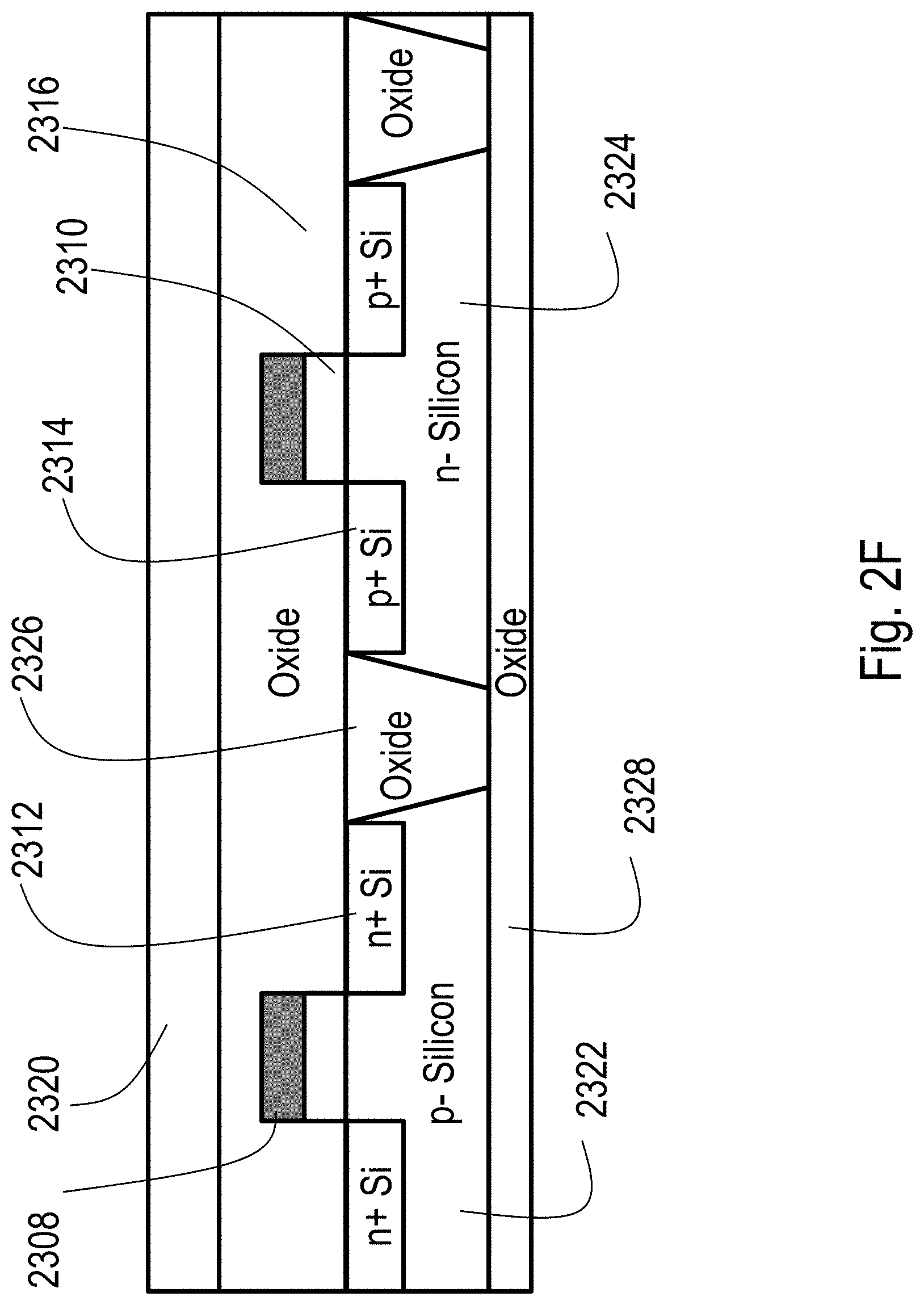
D00014
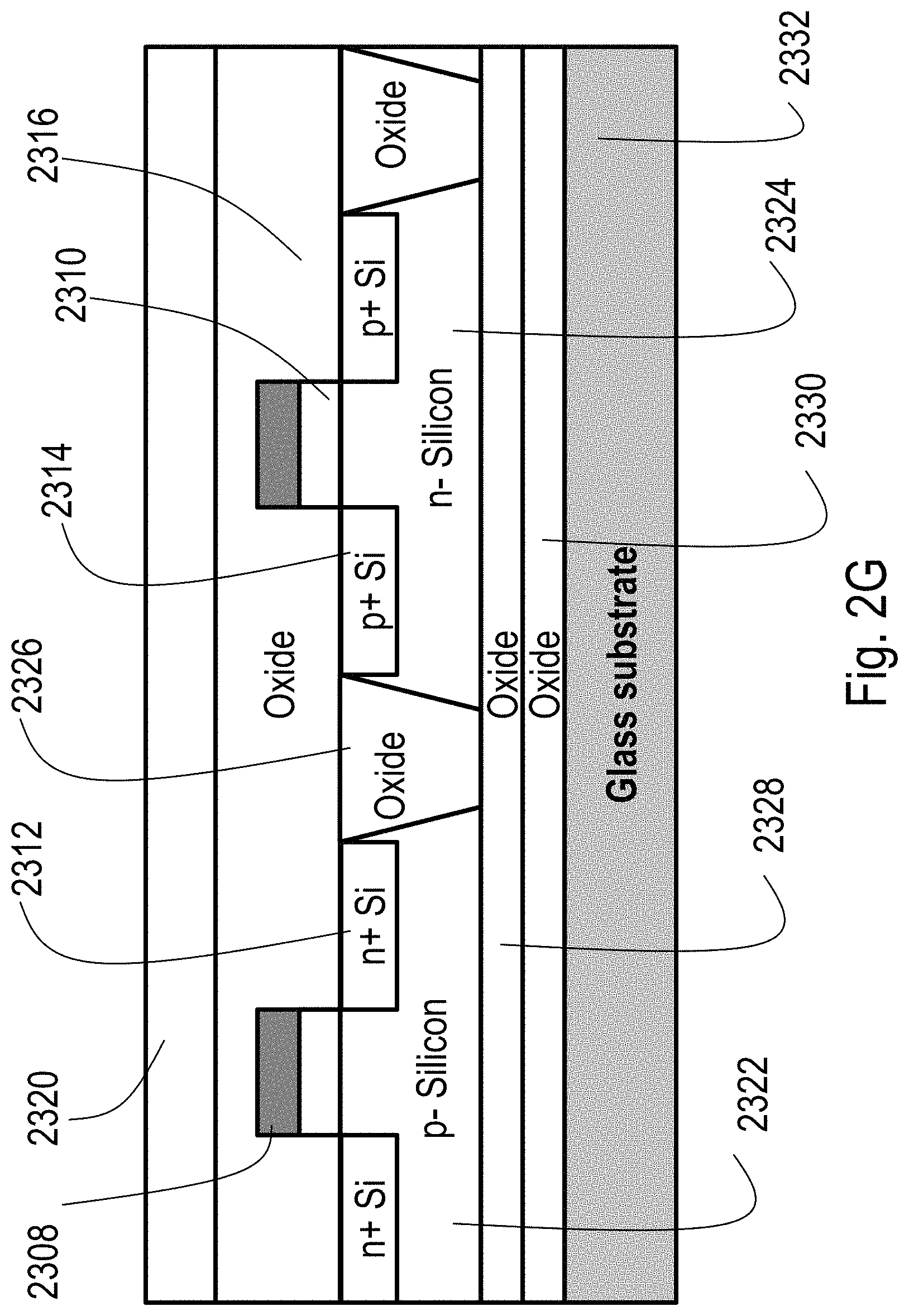
D00015
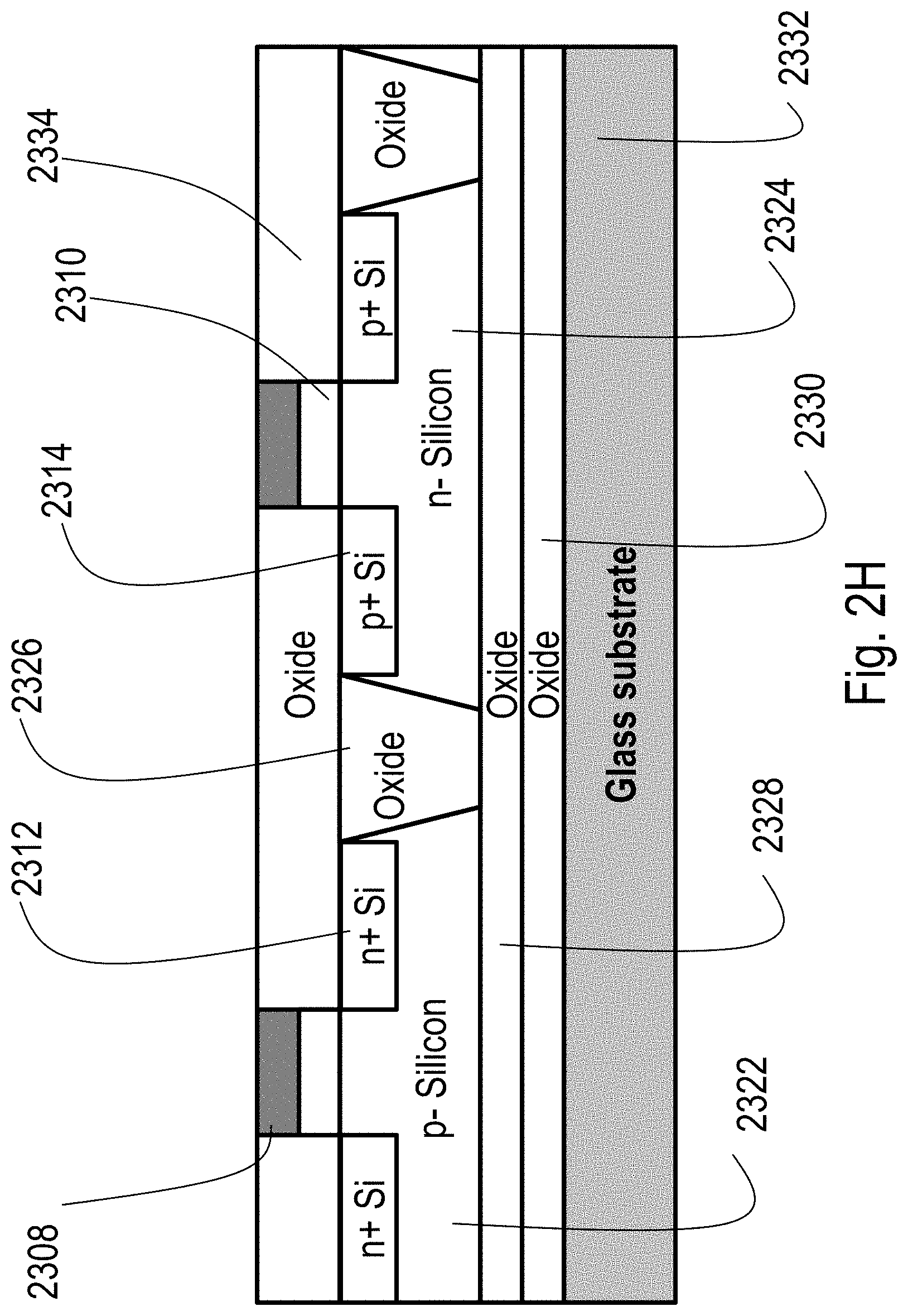
D00016
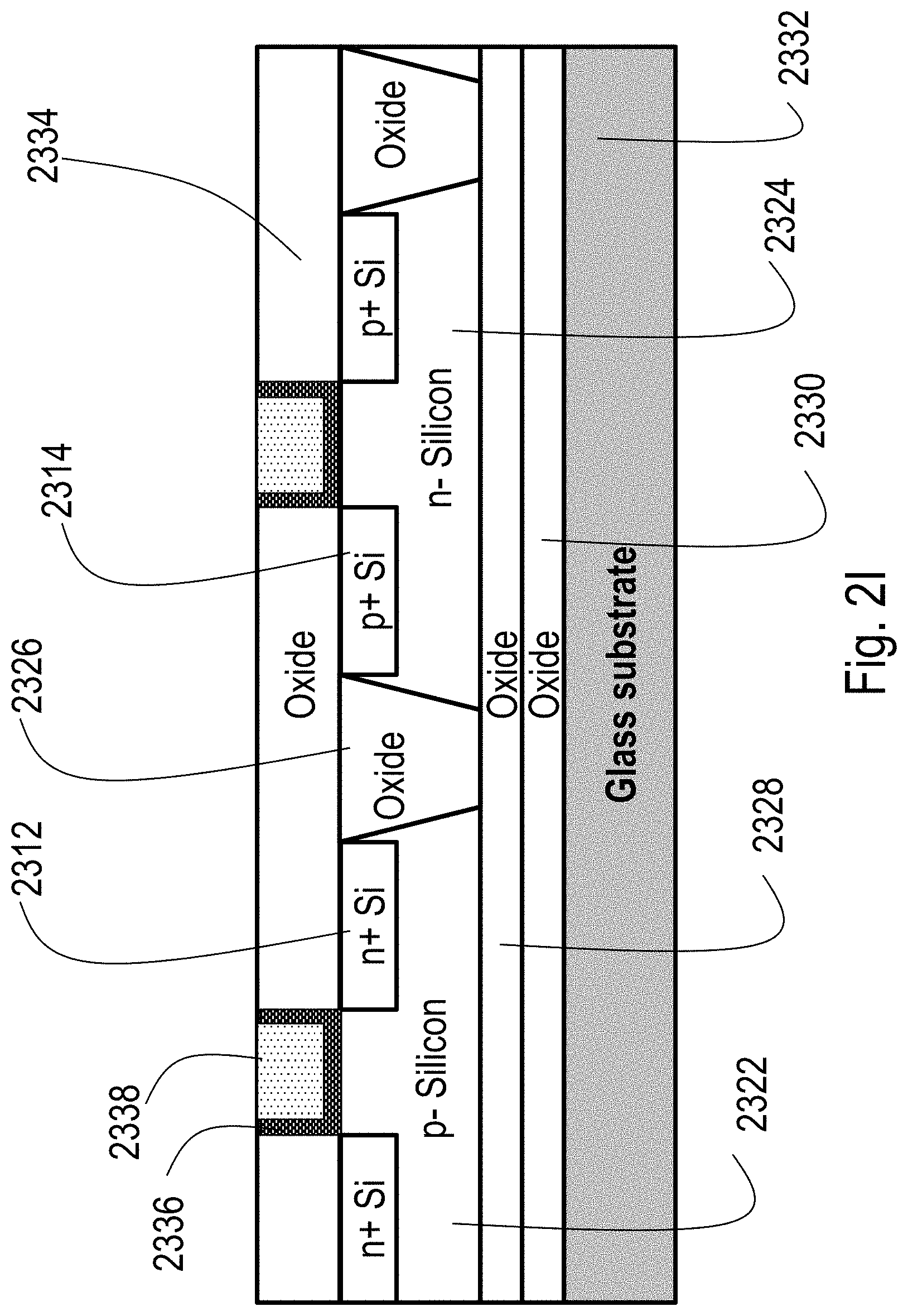
D00017
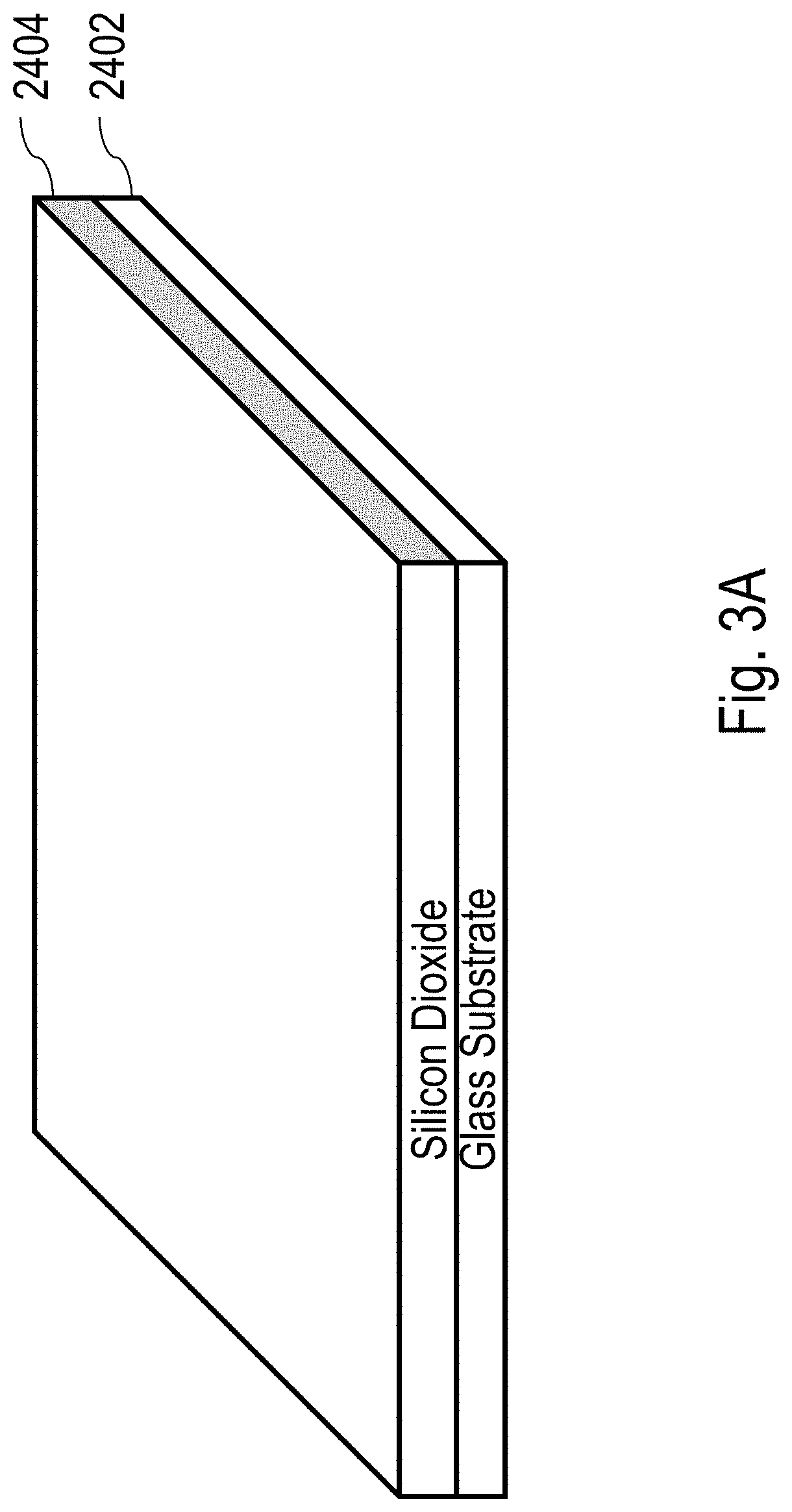
D00018
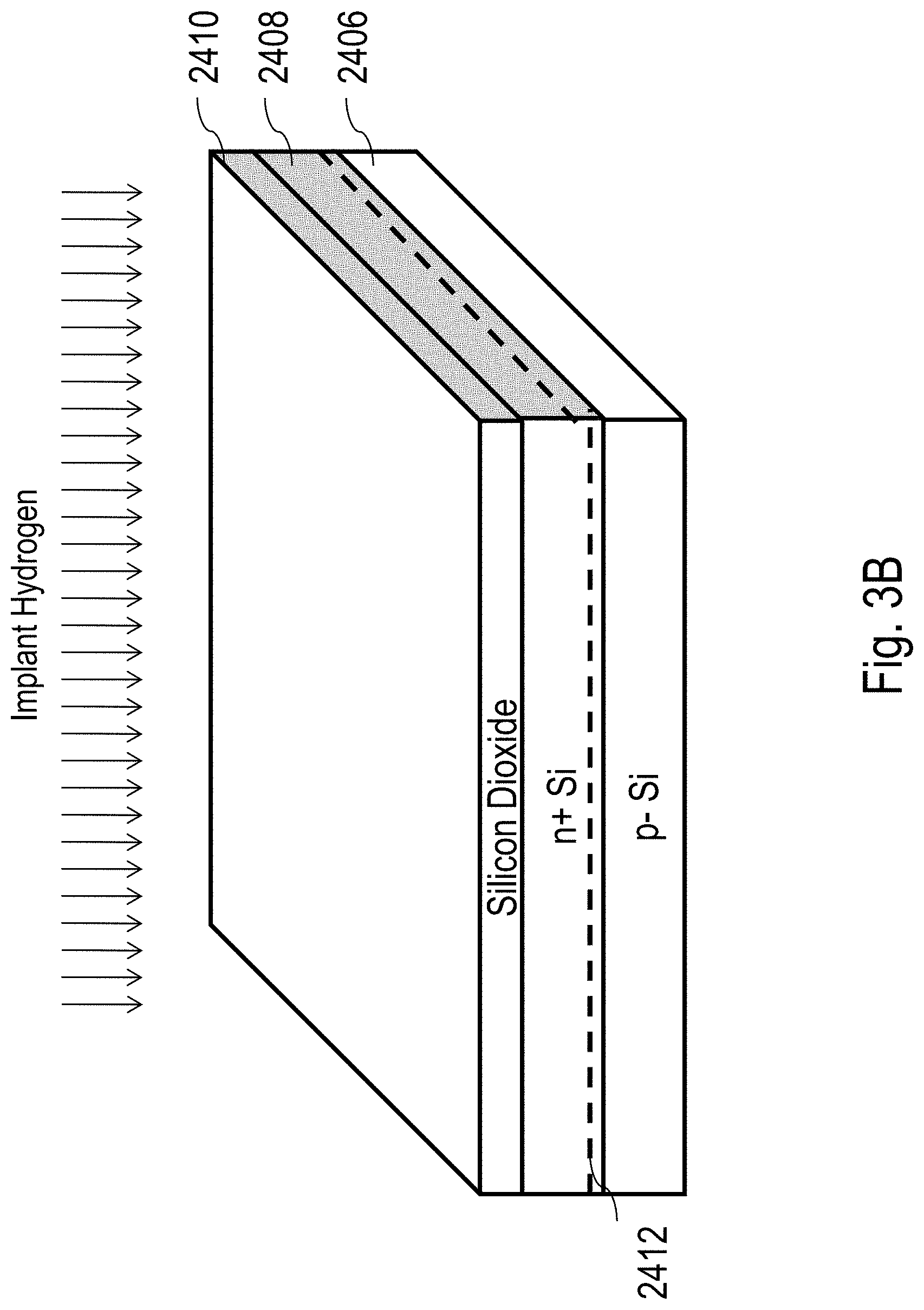
D00019

D00020

D00021

D00022

D00023

D00024

D00025
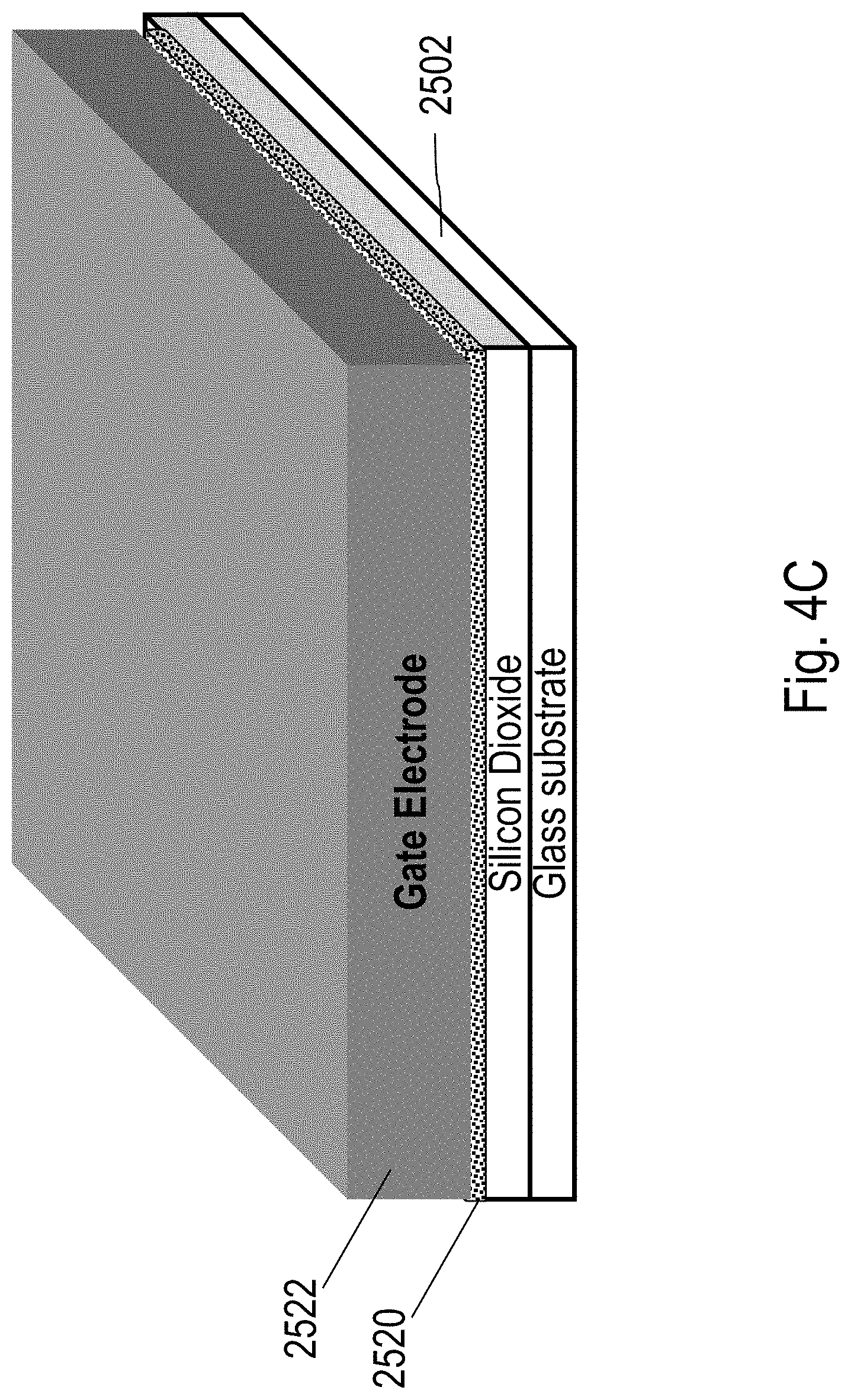
D00026
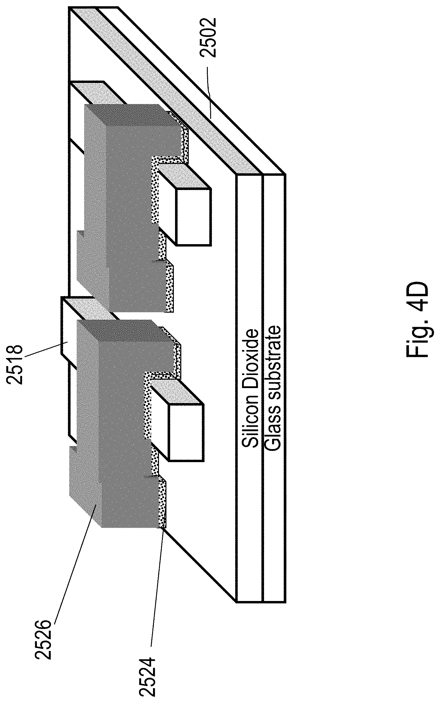
D00027

D00028
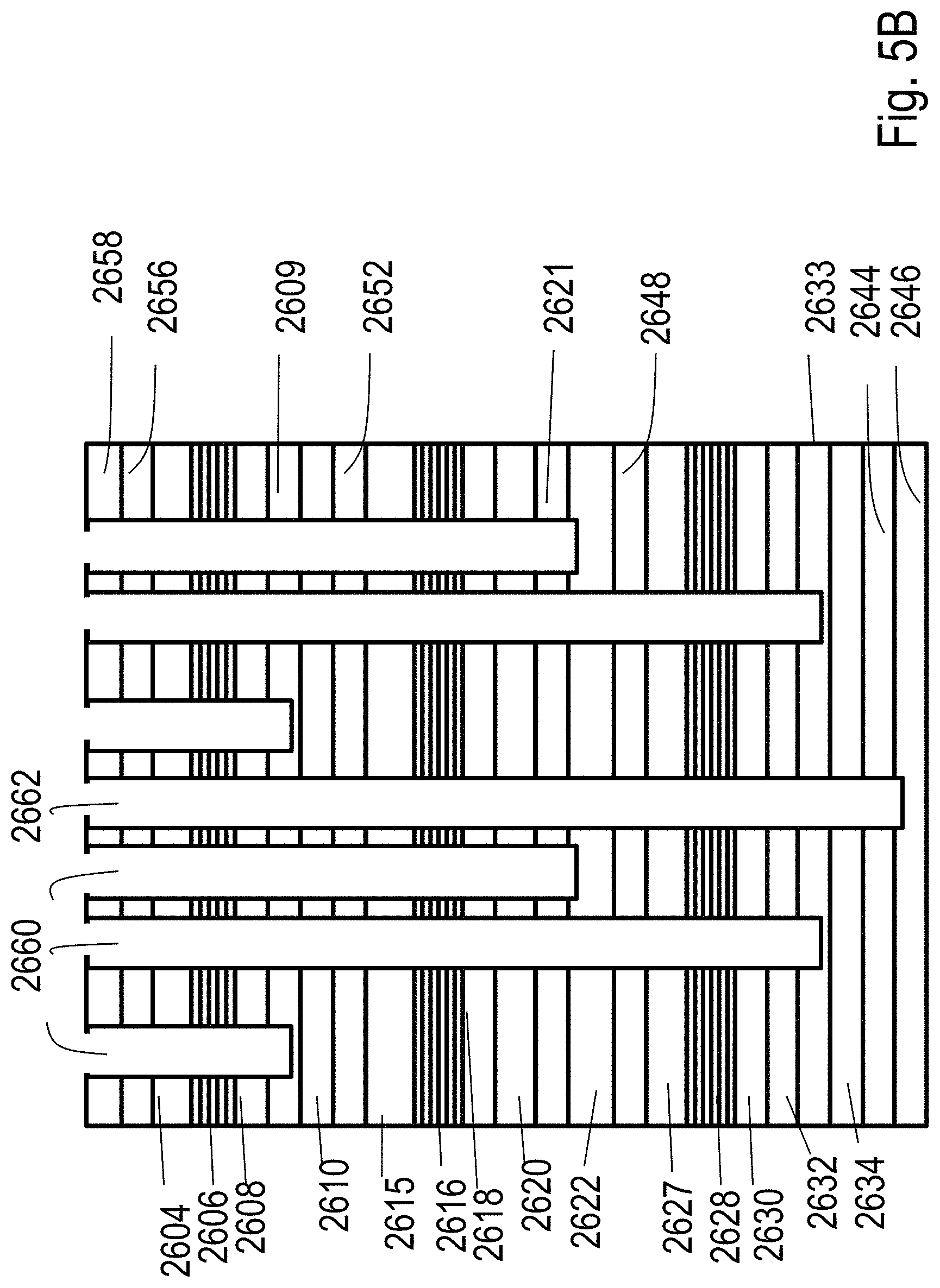
D00029
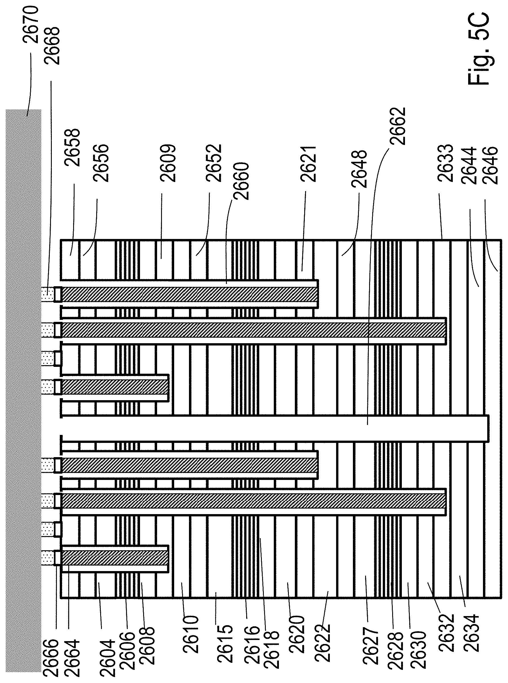
D00030
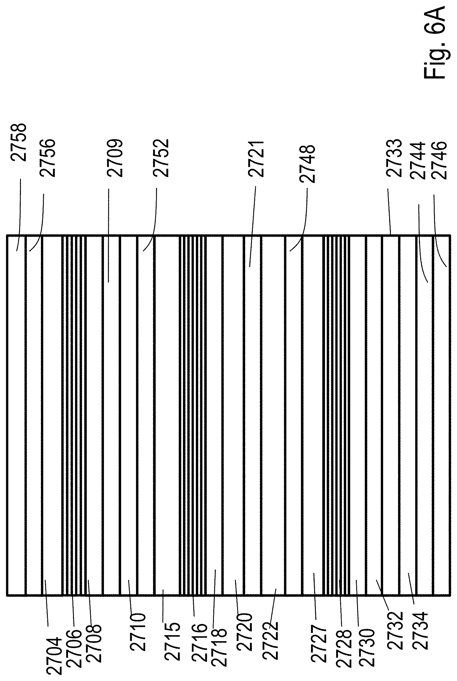
D00031

D00032
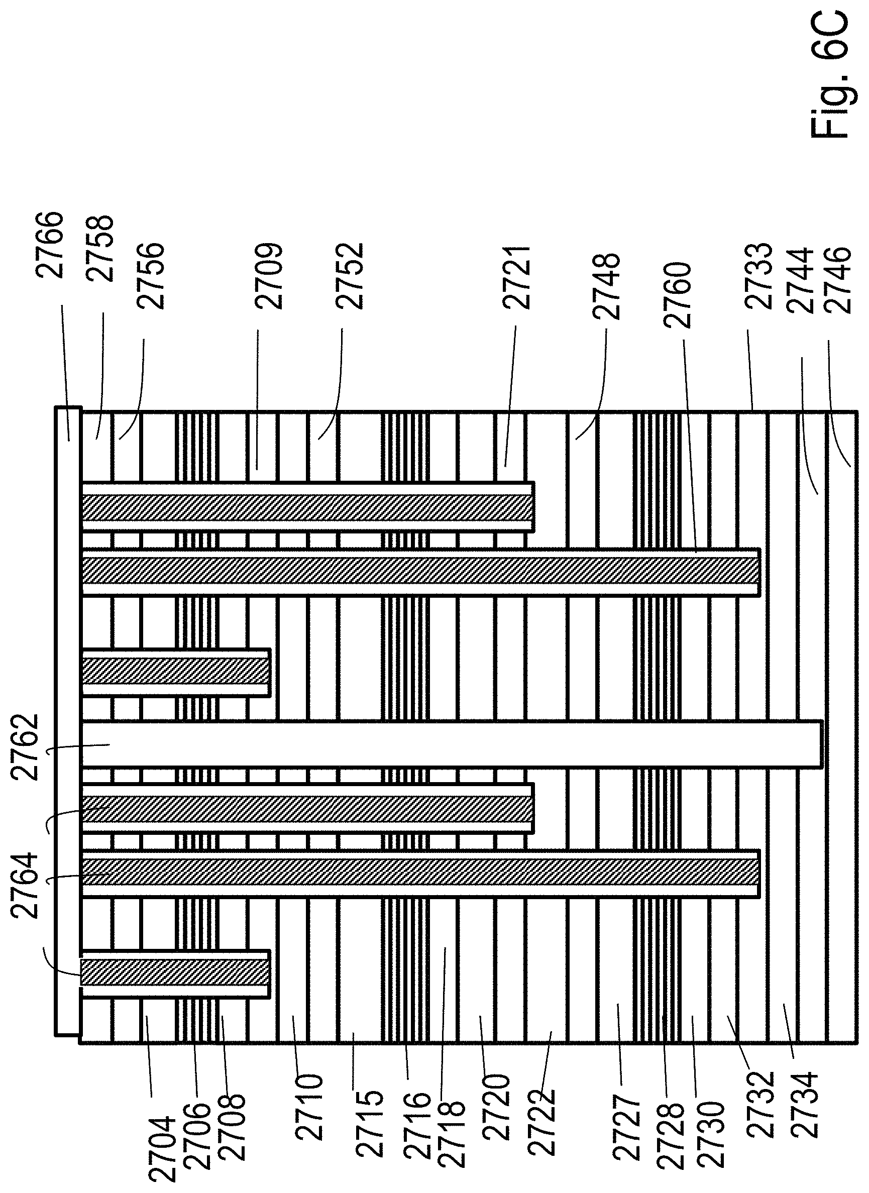
D00033
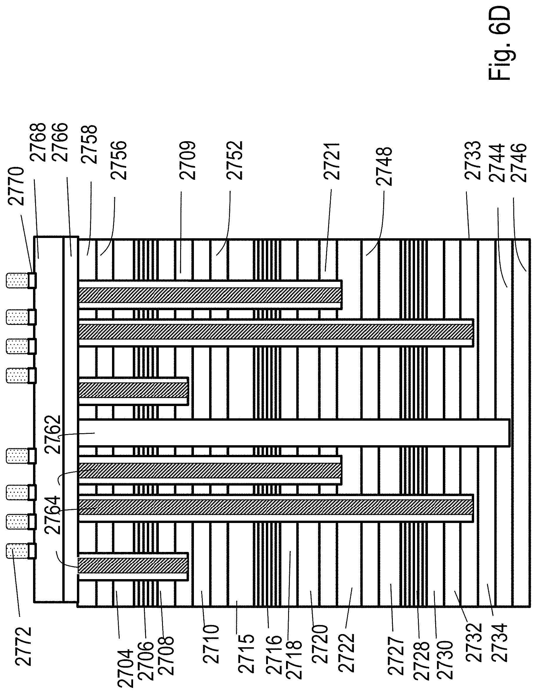
XML
uspto.report is an independent third-party trademark research tool that is not affiliated, endorsed, or sponsored by the United States Patent and Trademark Office (USPTO) or any other governmental organization. The information provided by uspto.report is based on publicly available data at the time of writing and is intended for informational purposes only.
While we strive to provide accurate and up-to-date information, we do not guarantee the accuracy, completeness, reliability, or suitability of the information displayed on this site. The use of this site is at your own risk. Any reliance you place on such information is therefore strictly at your own risk.
All official trademark data, including owner information, should be verified by visiting the official USPTO website at www.uspto.gov. This site is not intended to replace professional legal advice and should not be used as a substitute for consulting with a legal professional who is knowledgeable about trademark law.