Conductive stiffener, method of making a conductive stiffener, and conductive adhesive and encapsulation layers
McGrane , et al.
U.S. patent number 10,653,332 [Application Number 15/208,444] was granted by the patent office on 2020-05-19 for conductive stiffener, method of making a conductive stiffener, and conductive adhesive and encapsulation layers. This patent grant is currently assigned to MC10, Inc.. The grantee listed for this patent is MC10, Inc.. Invention is credited to Roozbeh Ghaffari, Bryan Keen, Stephen Lee, Monica Lin, Bryan McGrane, Jeffrey Model, Briana Morey, Milan Raj, Xianyan Wang, PingHung Wei.


| United States Patent | 10,653,332 |
| McGrane , et al. | May 19, 2020 |
Conductive stiffener, method of making a conductive stiffener, and conductive adhesive and encapsulation layers
Abstract
A device includes a flexible printed circuit board and one or more conductive stiffeners. The conductive stiffeners include a conductive surface that can be electrically connected to contact pads on the flexible printed circuit board. The wearable device can further include an adhesive layer or an encapsulation layer. The adhesive layer and the encapsulation layer can include conductive portions surrounded by non-conductive portions. The conductive portions can be aligned with the conductive stiffeners and together transmit electrical energy to the contact pads of the flexible printed circuit board.
| Inventors: | McGrane; Bryan (Cambridge, MA), Raj; Milan (Natick, MA), Wei; PingHung (Burlingame, MA), Morey; Briana (Somerville, MA), Ghaffari; Roozbeh (Cambridge, MA), Lin; Monica (San Jose, CA), Model; Jeffrey (Cambridge, MA), Wang; Xianyan (San Jose, CA), Keen; Bryan (Somerville, MA), Lee; Stephen (Ann Arbor, MI) | ||||||||||
|---|---|---|---|---|---|---|---|---|---|---|---|
| Applicant: |
|
||||||||||
| Assignee: | MC10, Inc. (Lexington,
MA) |
||||||||||
| Family ID: | 57775401 | ||||||||||
| Appl. No.: | 15/208,444 | ||||||||||
| Filed: | July 12, 2016 |
Prior Publication Data
| Document Identifier | Publication Date | |
|---|---|---|
| US 20170019988 A1 | Jan 19, 2017 | |
Related U.S. Patent Documents
| Application Number | Filing Date | Patent Number | Issue Date | ||
|---|---|---|---|---|---|
| 62194058 | Jul 17, 2015 | ||||
| Current U.S. Class: | 1/1 |
| Current CPC Class: | H05K 1/189 (20130101); A61B 5/0492 (20130101); A61B 5/0476 (20130101); A61B 5/0488 (20130101); A61B 5/6801 (20130101); A61B 5/0478 (20130101); A61B 5/0496 (20130101); A61B 5/0408 (20130101); A61B 2562/166 (20130101); A61B 5/053 (20130101); H05K 2201/10401 (20130101); H05K 2203/1327 (20130101); H05K 2201/10151 (20130101); H05K 1/0209 (20130101); A61B 5/01 (20130101); H05K 2201/2009 (20130101); A61B 5/0402 (20130101); H05K 1/0283 (20130101); H05K 2201/0969 (20130101); A61B 2562/164 (20130101); H05K 2201/10106 (20130101) |
| Current International Class: | H05K 1/18 (20060101); H05K 1/02 (20060101); A61B 5/0496 (20060101); A61B 5/00 (20060101); A61B 5/0476 (20060101); A61B 5/0492 (20060101); A61B 5/0478 (20060101); A61B 5/0408 (20060101); A61B 5/0488 (20060101); A61B 5/053 (20060101); A61B 5/01 (20060101); A61B 5/0402 (20060101) |
References Cited [Referenced By]
U.S. Patent Documents
| 3716861 | February 1973 | Root |
| 3805427 | April 1974 | Epstein |
| 3838240 | September 1974 | Schelhorn |
| 4278474 | July 1981 | Blakeslee |
| 4304235 | December 1981 | Kaufman |
| 4416288 | November 1983 | Freeman |
| 4658153 | April 1987 | Brosh |
| 5214000 | May 1993 | Chazan |
| 5272375 | December 1993 | Belopolsky |
| 5306917 | April 1994 | Black |
| 5326521 | July 1994 | East |
| 5331966 | July 1994 | Bennett |
| 5360987 | November 1994 | Shibib |
| 5471982 | May 1995 | Edwards |
| 5454270 | October 1995 | Brown |
| 5491651 | February 1996 | Janic |
| 5567975 | October 1996 | Walsh |
| 5580794 | December 1996 | Allen |
| 5617870 | April 1997 | Hastings |
| 5811790 | September 1998 | Endo |
| 5817008 | October 1998 | Rafert |
| 5907477 | May 1999 | Tuttle |
| 6063046 | May 2000 | Allum |
| 6265090 | July 2001 | Nishide |
| 6282960 | September 2001 | Samuels |
| 6343514 | February 2002 | Smith |
| 6387052 | May 2002 | Quinn |
| 6410971 | June 2002 | Otey |
| 6421016 | July 2002 | Phillips |
| 6455931 | September 2002 | Hamilton |
| 6567158 | May 2003 | Falcial |
| 6626940 | September 2003 | Crowley |
| 6641860 | November 2003 | Kaiserman |
| 6775906 | August 2004 | Silverbrook |
| 6784844 | August 2004 | Boakes |
| 6965160 | November 2005 | Cobbley |
| 6987314 | January 2006 | Yoshida |
| 7259030 | August 2007 | Daniels |
| 7265298 | September 2007 | Maghribi |
| 7302751 | December 2007 | Hamburgen |
| 7337012 | February 2008 | Maghribi |
| 7487587 | February 2009 | Vanfleteren |
| 7491892 | February 2009 | Wagner |
| 7521292 | April 2009 | Rogers |
| 7557367 | July 2009 | Rogers |
| 7618260 | November 2009 | Daniel |
| 7622367 | November 2009 | Nuzzo |
| 7727228 | June 2010 | Abboud |
| 7739791 | June 2010 | Brandenburg |
| 7759167 | July 2010 | Vanfleteren |
| 7815095 | October 2010 | Fujisawa |
| 7960246 | June 2011 | Flamand |
| 7982296 | July 2011 | Nuzzo |
| 8097926 | January 2012 | De Graff |
| 8198621 | June 2012 | Rogers |
| 8207473 | June 2012 | Axisa |
| 8217381 | July 2012 | Rogers |
| 8372726 | February 2013 | De Graff |
| 8389862 | March 2013 | Arora |
| 8431828 | April 2013 | Vanfleteren |
| 8440546 | May 2013 | Nuzzo |
| 8536667 | September 2013 | De Graff |
| 8552299 | October 2013 | Rogers |
| 8618656 | December 2013 | Oh |
| 8664699 | March 2014 | Nuzzo |
| 8679888 | March 2014 | Rogers |
| 8729524 | May 2014 | Rogers |
| 8754396 | June 2014 | Rogers |
| 8865489 | October 2014 | Rogers |
| 8886334 | November 2014 | Ghaffari |
| 8905772 | December 2014 | Rogers |
| 9012784 | April 2015 | Arora |
| 9082025 | July 2015 | Fastert |
| 9105555 | August 2015 | Rogers |
| 9105782 | August 2015 | Rogers |
| 9119533 | September 2015 | Ghaffari |
| 9123614 | September 2015 | Graff |
| 9159635 | October 2015 | Elolampi |
| 9168094 | October 2015 | Lee |
| 9171794 | October 2015 | Rafferty |
| 9186060 | November 2015 | De Graff |
| 9226402 | December 2015 | Hsu |
| 9247637 | January 2016 | Hsu |
| 9289132 | March 2016 | Ghaffari |
| 9295842 | March 2016 | Ghaffari |
| 9324733 | April 2016 | Rogers |
| 9372123 | June 2016 | Li |
| 9408305 | August 2016 | Hsu |
| 10321561 | June 2019 | Hu |
| 2001/0012918 | August 2001 | Swanson |
| 2001/0021867 | September 2001 | Kordis |
| 2002/0026127 | February 2002 | Balbierz |
| 2002/0082515 | June 2002 | Campbell |
| 2002/0094701 | July 2002 | Biegelsen |
| 2002/0113739 | August 2002 | Howard |
| 2002/0128700 | September 2002 | Cross, Jr. |
| 2002/0145467 | October 2002 | Minch |
| 2002/0151934 | October 2002 | Levine |
| 2002/0158330 | October 2002 | Moon |
| 2003/0017848 | January 2003 | Engstrom |
| 2003/0045025 | March 2003 | Coyle |
| 2003/0090000 | May 2003 | Caletka |
| 2003/0097165 | May 2003 | Krulevitch |
| 2003/0120271 | June 2003 | Burnside |
| 2003/0146017 | August 2003 | Fan |
| 2003/0162507 | August 2003 | Vatt |
| 2003/0168725 | September 2003 | Warner |
| 2003/0214408 | November 2003 | Grajales |
| 2003/0236455 | December 2003 | Swanson |
| 2004/0006264 | January 2004 | Mojarradi |
| 2004/0007376 | January 2004 | Urdahl |
| 2004/0085469 | May 2004 | Johnson |
| 2004/0092806 | May 2004 | Sagon |
| 2004/0106334 | June 2004 | Suzuki |
| 2004/0135094 | July 2004 | Niigaki |
| 2004/0138558 | July 2004 | Dunki-Jacobs |
| 2004/0149921 | August 2004 | Smyk |
| 2004/0178466 | September 2004 | Merrill |
| 2004/0192082 | September 2004 | Wagner |
| 2004/0201134 | October 2004 | Kawai |
| 2004/0203486 | October 2004 | Shepherd |
| 2004/0221370 | November 2004 | Hannula |
| 2004/0243204 | December 2004 | Maghribi |
| 2005/0021103 | January 2005 | DiLorenzo |
| 2005/0029680 | February 2005 | Jung |
| 2005/0067293 | March 2005 | Naito |
| 2005/0070778 | March 2005 | Lackey |
| 2005/0096513 | May 2005 | Ozguz |
| 2005/0113744 | May 2005 | Donoghue |
| 2005/0139683 | June 2005 | Yi |
| 2005/0171524 | August 2005 | Stern |
| 2005/0203366 | September 2005 | Donoghue |
| 2005/0248312 | November 2005 | Cao |
| 2005/0285262 | December 2005 | Knapp |
| 2006/0003709 | January 2006 | Wood |
| 2006/0038182 | February 2006 | Rogers |
| 2006/0071349 | April 2006 | Tokushige |
| 2006/0084394 | April 2006 | Engstrom |
| 2006/0106321 | May 2006 | Lewinsky |
| 2006/0128346 | June 2006 | Yasui |
| 2006/0154398 | July 2006 | Qing |
| 2006/0160560 | July 2006 | Josenhans |
| 2006/0248946 | November 2006 | Howell |
| 2006/0257945 | November 2006 | Masters |
| 2006/0264767 | November 2006 | Shennib |
| 2006/0270135 | November 2006 | Chrysler |
| 2006/0286785 | December 2006 | Rogers |
| 2007/0027514 | February 2007 | Gerber |
| 2007/0031283 | February 2007 | Davis |
| 2007/0108389 | May 2007 | Makela |
| 2007/0113399 | May 2007 | Kumar |
| 2007/0123756 | May 2007 | Kitajima |
| 2007/0270672 | November 2007 | Hayter |
| 2008/0036097 | February 2008 | Ito |
| 2008/0046080 | February 2008 | Vanden Bulcke |
| 2008/0074383 | March 2008 | Dean |
| 2008/0096620 | April 2008 | Lee |
| 2008/0099898 | May 2008 | Cui |
| 2008/0139894 | June 2008 | Szydlo-Moore |
| 2008/0157235 | July 2008 | Rogers |
| 2008/0188912 | August 2008 | Stone |
| 2008/0193749 | August 2008 | Thompson |
| 2008/0204021 | August 2008 | Leussler |
| 2008/0211087 | September 2008 | Mueller-Hipper |
| 2008/0237840 | October 2008 | Alcoe |
| 2008/0259576 | October 2008 | Johnson |
| 2008/0262381 | October 2008 | Kolen |
| 2008/0287167 | November 2008 | Caine |
| 2008/0313552 | December 2008 | Buehler |
| 2009/0000377 | January 2009 | Shipps |
| 2009/0001550 | January 2009 | Yonggang |
| 2009/0015560 | January 2009 | Robinson |
| 2009/0017884 | January 2009 | Rotschild |
| 2009/0048556 | February 2009 | Durand |
| 2009/0088750 | April 2009 | Hushka |
| 2009/0107704 | April 2009 | Vanfleteren |
| 2009/0154736 | June 2009 | Lee |
| 2009/0178274 | July 2009 | Kumar |
| 2009/0184254 | July 2009 | Miura |
| 2009/0204168 | August 2009 | Kallmeyer |
| 2009/0215385 | August 2009 | Waters |
| 2009/0225751 | September 2009 | Koenck |
| 2009/0261828 | October 2009 | Nordmeyer-Massner |
| 2009/0273909 | November 2009 | Shin |
| 2009/0283891 | November 2009 | Dekker |
| 2009/0291508 | November 2009 | Babu |
| 2009/0294803 | December 2009 | Nuzzo |
| 2009/0322480 | December 2009 | Benedict |
| 2010/0002402 | January 2010 | Rogers |
| 2010/0059863 | March 2010 | Rogers |
| 2010/0072577 | March 2010 | Nuzzo |
| 2010/0073669 | March 2010 | Colvin |
| 2010/0087782 | April 2010 | Ghaffari |
| 2010/0090781 | April 2010 | Yamamoto |
| 2010/0090824 | April 2010 | Rowell |
| 2010/0116526 | May 2010 | Arora |
| 2010/0117660 | May 2010 | Douglas |
| 2010/0178722 | July 2010 | De Graff |
| 2010/0207265 | August 2010 | Muthukumar |
| 2010/0245011 | September 2010 | Chatzopoulos |
| 2010/0271191 | October 2010 | De Graff |
| 2010/0298895 | November 2010 | Ghaffari |
| 2010/0317132 | December 2010 | Rogers |
| 2010/0321161 | December 2010 | Isabell |
| 2010/0327387 | December 2010 | Kasai |
| 2011/0011179 | January 2011 | Gustafsson |
| 2011/0034912 | February 2011 | De Graff |
| 2011/0051384 | March 2011 | Kriechbaum |
| 2011/0054583 | March 2011 | Litt |
| 2011/0098583 | April 2011 | Pandia |
| 2011/0101789 | May 2011 | Salter |
| 2011/0121822 | May 2011 | Parsche |
| 2011/0140897 | June 2011 | Purks |
| 2011/0175735 | July 2011 | Forster |
| 2011/0184320 | July 2011 | Shipps |
| 2011/0215931 | September 2011 | Callsen |
| 2011/0218756 | September 2011 | Callsen |
| 2011/0218757 | September 2011 | Callsen |
| 2011/0220890 | September 2011 | Nuzzo |
| 2011/0263950 | October 2011 | Larson |
| 2011/0277813 | November 2011 | Rogers |
| 2011/0284268 | November 2011 | Palaniswamy |
| 2011/0306851 | December 2011 | Wang |
| 2012/0016258 | January 2012 | Webster |
| 2012/0051005 | March 2012 | Vanfleteren |
| 2012/0052268 | March 2012 | Axisa |
| 2012/0065937 | March 2012 | De Graff |
| 2012/0074546 | March 2012 | Chong |
| 2012/0087216 | April 2012 | Keung |
| 2012/0091594 | April 2012 | Landesberger |
| 2012/0092178 | April 2012 | Callsen |
| 2012/0092222 | April 2012 | Kato |
| 2012/0101413 | April 2012 | Beetel |
| 2012/0101538 | April 2012 | Ballakur |
| 2012/0108012 | May 2012 | Yasuda |
| 2012/0126418 | May 2012 | Feng |
| 2012/0157804 | June 2012 | Rogers |
| 2012/0172697 | July 2012 | Urman |
| 2012/0178367 | July 2012 | Matsumoto |
| 2012/0226130 | September 2012 | De Graff |
| 2012/0244848 | September 2012 | Ghaffari |
| 2012/0256308 | October 2012 | Helin |
| 2012/0316455 | December 2012 | Rahman |
| 2012/0327608 | December 2012 | Rogers |
| 2013/0041235 | February 2013 | Rogers |
| 2013/0099358 | April 2013 | Elolampi |
| 2013/0100618 | April 2013 | Rogers |
| 2013/0116520 | May 2013 | Roham |
| 2013/0118255 | May 2013 | Callsen |
| 2013/0150693 | June 2013 | D'angelo |
| 2013/0185003 | July 2013 | Carbeck |
| 2013/0192356 | August 2013 | De Graff |
| 2013/0200268 | August 2013 | Rafferty |
| 2013/0211761 | August 2013 | Brandsma |
| 2013/0214300 | August 2013 | Lerman |
| 2013/0215467 | August 2013 | Fein |
| 2013/0225965 | August 2013 | Ghaffari |
| 2013/0237150 | September 2013 | Royston |
| 2013/0245388 | September 2013 | Rafferty |
| 2013/0274562 | October 2013 | Ghaffari |
| 2013/0313713 | November 2013 | Arora |
| 2013/0316442 | November 2013 | Meurville |
| 2013/0316487 | November 2013 | De Graff |
| 2013/0316645 | November 2013 | Li |
| 2013/0320503 | December 2013 | Nuzzo |
| 2013/0321373 | December 2013 | Yoshizumi |
| 2013/0328219 | December 2013 | Chau |
| 2014/0001058 | January 2014 | Ghaffari |
| 2014/0012160 | January 2014 | Ghaffari |
| 2014/0012242 | January 2014 | Lee |
| 2014/0022746 | January 2014 | Hsu |
| 2014/0039290 | February 2014 | De Graff |
| 2014/0097944 | April 2014 | Fastert |
| 2014/0110859 | April 2014 | Rafferty |
| 2014/0140020 | May 2014 | Rogers |
| 2014/0188426 | July 2014 | Fastert |
| 2014/0191236 | July 2014 | Nuzzo |
| 2014/0216524 | August 2014 | Rogers |
| 2014/0240932 | August 2014 | Hsu |
| 2014/0249520 | September 2014 | Ghaffari |
| 2014/0303452 | October 2014 | Ghaffari |
| 2014/0303680 | October 2014 | Donnelly |
| 2014/0340857 | November 2014 | Hsu |
| 2014/0374872 | December 2014 | Rogers |
| 2014/0375465 | December 2014 | Fenuccio |
| 2015/0001462 | January 2015 | Rogers |
| 2015/0019135 | January 2015 | Kacyvenski |
| 2015/0025394 | January 2015 | Hong |
| 2015/0035680 | February 2015 | Li |
| 2015/0069617 | March 2015 | Arora |
| 2015/0099976 | April 2015 | Ghaffari |
| 2015/0100135 | April 2015 | Ives |
| 2015/0194817 | July 2015 | Lee |
| 2015/0237711 | August 2015 | Rogers |
| 2015/0241288 | August 2015 | Keen |
| 2015/0260713 | September 2015 | Ghaffari |
| 2015/0272652 | October 2015 | Ghaffari |
| 2015/0286913 | October 2015 | Fastert |
| 2015/0320472 | November 2015 | Ghaffari |
| 2015/0335254 | November 2015 | Elolampi |
| 2015/0342036 | November 2015 | Fastert |
| 2016/0027834 | January 2016 | de Graff |
| 2016/0035658 | February 2016 | Kessler |
| 2016/0045162 | February 2016 | De Graff |
| 2016/0081192 | March 2016 | Hsu |
| 2016/0086909 | March 2016 | Garlock |
| 2016/0095652 | April 2016 | Lee |
| 2016/0099214 | April 2016 | Dalal |
| 2016/0099227 | April 2016 | Dalal |
| 2016/0111353 | April 2016 | Rafferty |
| 2016/0135740 | May 2016 | Ghaffari |
| 2016/0213262 | July 2016 | Ghaffari |
| 2016/0213424 | July 2016 | Ghaffari |
| 2016/0228640 | August 2016 | Pindado |
| 2016/0232807 | August 2016 | Ghaffari |
| 2016/0240061 | August 2016 | Li |
| 2016/0249174 | August 2016 | Patel |
| 2016/0256070 | September 2016 | Murphy |
| 2017/0086291 | March 2017 | Cotton |
| 2019/0087622 | March 2019 | Benkley, III |
| 0585670 | Mar 1994 | EP | |||
| 0779059 | Jun 1997 | EP | |||
| 1808124 | Jul 2007 | EP | |||
| 2259062 | Dec 2010 | EP | |||
| 05-087511 | Apr 1993 | JP | |||
| 2005-052212 | Mar 2005 | JP | |||
| 2009-170173 | Jul 2009 | JP | |||
| WO 1999/038211 | Jul 1999 | WO | |||
| WO 2005/122285 | Dec 2005 | WO | |||
| WO 2003/021679 | Mar 2006 | WO | |||
| WO 2007/003019 | Jan 2007 | WO | |||
| WO 2007/024983 | Mar 2007 | WO | |||
| WO 2007/116344 | Oct 2007 | WO | |||
| WO 2007/136726 | Nov 2007 | WO | |||
| WO 2008/030960 | Mar 2008 | WO | |||
| WO 2009/111641 | Sep 2009 | WO | |||
| WO 2009/114689 | Sep 2009 | WO | |||
| WO 2010/036807 | Apr 2010 | WO | |||
| WO 2010/042653 | Apr 2010 | WO | |||
| WO 2010/042957 | Apr 2010 | WO | |||
| WO 2010/046883 | Apr 2010 | WO | |||
| WO 2010/056857 | May 2010 | WO | |||
| WO 2010/081137 | Jul 2010 | WO | |||
| WO 2010/082993 | Jul 2010 | WO | |||
| WO 2010/102310 | Sep 2010 | WO | |||
| WO 2010/132552 | Nov 2010 | WO | |||
| WO 2011/003181 | Jan 2011 | WO | |||
| WO 2011/041727 | Apr 2011 | WO | |||
| WO 2011/084450 | Jul 2011 | WO | |||
| WO 2011/084709 | Jul 2011 | WO | |||
| WO 2011/127331 | Oct 2011 | WO | |||
| WO 2012/125494 | Sep 2012 | WO | |||
| WO 2012/166686 | Dec 2012 | WO | |||
| WO 2013/010171 | Jan 2013 | WO | |||
| WO 2013/022853 | Feb 2013 | WO | |||
| WO 2013/033724 | Mar 2013 | WO | |||
| WO 2013/034987 | Mar 2013 | WO | |||
| WO 2013/049716 | Apr 2013 | WO | |||
| WO 2013/052919 | Apr 2013 | WO | |||
| WO 2013/170032 | Nov 2013 | WO | |||
| WO 2014/007871 | Jan 2014 | WO | |||
| WO 2014/058473 | Apr 2014 | WO | |||
| WO 2014/059032 | Apr 2014 | WO | |||
| WO 2014/106041 | Jul 2014 | WO | |||
| WO 2014/110176 | Jul 2014 | WO | |||
| WO 2014/130928 | Aug 2014 | WO | |||
| WO 2014/130931 | Aug 2014 | WO | |||
| WO 2014/186467 | Nov 2014 | WO | |||
| WO 2014/197443 | Dec 2014 | WO | |||
| WO 2014/205434 | Dec 2014 | WO | |||
| WO 2015/021039 | Feb 2015 | WO | |||
| WO 2015/054312 | Apr 2015 | WO | |||
| WO 2015/077559 | May 2015 | WO | |||
| WO 2015/080991 | Jun 2015 | WO | |||
| WO 2015/102951 | Jul 2015 | WO | |||
| WO 2015/103483 | Jul 2015 | WO | |||
| WO 2015/103580 | Jul 2015 | WO | |||
| WO 2015/127458 | Aug 2015 | WO | |||
| WO 2015/134588 | Sep 2015 | WO | |||
| WO 2015/138712 | Sep 2015 | WO | |||
| WO 2016/048888 | Mar 2016 | WO | |||
| WO 2016/054512 | Apr 2016 | WO | |||
| WO 2016/057318 | Apr 2016 | WO | |||
| WO 2016/081244 | May 2016 | WO | |||
| WO 2016/0127050 | Aug 2016 | WO | |||
| WO 2016/134306 | Aug 2016 | WO | |||
Other References
|
International Search Report dated Dec. 9, 2016 which issued in International Patent Application No. PCT/US2016/041927 (5 pages). cited by applicant . Written Opinion dated Dec. 9, 2016 which issued in International Patent Application No. PCT/US2016/041927 (9 pages). cited by applicant . Carvalhal et al., "Electrochemical Detection in a Paper-Based Separation Device", Analytical Chemistry, vol. 82, No. 3, (1162-1165) (4 pages) (Jan. 7, 2010). cited by applicant . Demura et al "Immobilization of Glucose Oxidase with Bombyx Mori Silk Fibroin by Only Stretching Treatment and its Application to Glucose Sensor," Biotechnology and Bioengineering, vol. 33, 598-603 (6 pages) (1989). cited by applicant . Ellerbee et al., "Quantifying Colorimetric Assays in Paper-Based Microfluidic Devices by Measuring the Transmission of Light through Paper," Analytical Chemistry, vol. 81, No. 20 8447-8452, (6 pages) (Oct. 15, 2009). cited by applicant . Halsted, "Ligature and Suture Material," Journal of the American Medical Association, vol. LX, No. 15, 1119-1126, (8 pages) (Apr. 12, 1913). cited by applicant . Kim et al., "Complementary Metal Oxide Silicon Integrated Circuits Incorporating Monolithically Integrated Stretchable Wavy Interconnects," Applied Physics Letters, vol. 93, 044102-044102.3 (3 pages) (Jul. 31, 2008). cited by applicant . Kim et al., "Dissolvable Films of Silk Fibroin for Ultrathin Conformal Bio-Integrated Electronics," Nature, 1-8 (8 pages) (Apr. 18, 2010). cited by applicant . Kim et al., "Materials and Noncoplanar Mesh Designs for Integrated Circuits with Linear Elastic Responses to Extreme Mechanical Deformations," PNAS, vol. 105, No. 48, 18675-18680 (6 pages) (Dec. 2, 2008). cited by applicant . Kim et al., "Stretchable and Foldable Silicon Integrated Circuits," Science, vol. 320, 507-511 (5 pages) (Apr. 25, 2008). cited by applicant . Kim et al., "Electrowetting on Paper for Electronic Paper Display," ACS Applied Materials & Interfaces, vol. 2, No. 11, (3318-3323) (6 pages) (Nov. 24, 2010). cited by applicant . Ko et al., "A Hemispherical Electronic Eye Camera Based on Compressible Silicon Optoelectronics," Nature, vol. 454, 748-753 (6 pages) (Aug. 7, 2008). cited by applicant . Lawrence et al., "Bioactive Silk Protein Biomaterial Systems for Optical Devices," Biomacromolecules, vol. 9, 1214-1220 (7 pages) (Nov. 4, 2008). cited by applicant . Meitl et al., "Transfer Printing by Kinetic Control of Adhesion to an Elastomeric Stamp," Nature, vol. 5, 33-38 (6 pages) (Jan. 2006). cited by applicant . Omenetto et al., "A New Route for Silk," Nature Photonics, vol. 2, 641-643 (3 pages) (Nov. 2008). cited by applicant . Omenetto et al., "New Opportunities for an Ancient Material," Science, vol. 329, 528-531 (5 pages) (Jul. 30, 2010). cited by applicant . Siegel et al., "Foldable Printed Circuit Boards on Paper Substrates," Advanced Functional Materials, vol. 20, No. 1, 28-35, (8 pages) (Jan. 8, 2010). cited by applicant . Tsukada et al., "Structural Changes of Silk Fibroin Membranes Induced by Immersion in Methanol Aqueous Solutions," Journal of Polymer Science, vol. 32, 961-968 (8 pages) (1994). cited by applicant . Wang et al., "Controlled Release From Multilayer Silk Biomaterial Coatings to Modulate Vascular Cell Responses" Biomaterials, 29, 894-903 (10 pages) (Nov. 28, 2008). cited by applicant . Wikipedia, "Ball bonding" article [online]. Cited in PCT/US2015/051210 search report dated Mar. 1, 2016 with the following information "Jun. 15, 2011 [retrieved on Nov. 15, 2015}. Retrieved Dec. 29, 2018 from the Internet: <URL: https://web.archive.org/web/20110615221003/hltp://en.wikipedia.org/wiki/B- all_bonding>., entire document, especially para 1, 4, 5, 6," 2 pages, last page says ("last modified on May 11, 2011"). cited by applicant. |
Primary Examiner: Milakovich; Nathan
Attorney, Agent or Firm: Nixon Peabody LLP
Parent Case Text
CROSS-REFERENCE TO RELATED APPLICATION
This application claims the benefit of and priority to U.S. Application No. 62/194,058, filed Jul. 17, 2015, and entitled, "CONDUCTIVE STIFFENER, METHOD OF MAKING A CONDUCTIVE STIFFENER, AND CONDUCTIVE ADHESIVE AND ENCAPSULATION LAYERS," which is hereby incorporated by reference herein in its entirety.
Claims
What is claimed is:
1. A device comprising: a flexible printed circuit board having a plurality of discrete operative devices electrically interconnected and one or more contact pads on a backside of the flexible printed circuit board; and a plurality of conductive stiffeners affixed to the backside of the flexible printed circuit board, each conductive stiffener electrically connecting at least one contact pad of the flexible printed circuit board to a bottom surface of the conductive stiffener and comprising: a non-conductive substrate sheet; a hole through the non-conductive substrate sheet; and a conductive material forming a pad on a bottom surface of the non-conductive substrate sheet and lining the hole, wherein the pad of conductive material is electrically connected to a top surface of the non-conductive substrate sheet through the conductive material lining the hole, wherein the conductive material forms a pad on the top surface of the non-conductive substrate sheet, and the pad of conductive material on the top surface comprises a thermal relief pattern in the conductive material surrounding the hole.
2. The device of claim 1, further comprising an encapsulation layer encapsulating the flexible printed circuit board and the plurality of conductive stiffeners.
3. The device of claim 2, wherein the encapsulation layer comprises non-conductive areas surrounding conductive areas, and the conductive areas are aligned with the bottom surfaces of the conductive stiffeners.
4. The device of claim 2, wherein a bottom surface of each conductive stiffener includes one or more indentations that interface with the encapsulation layer to mechanically couple the encapsulation layer to the plurality of conductive stiffeners.
5. The device of claim 4, wherein the one or more indentations are vertical interconnects accesses.
6. The device of claim 2, wherein a bottom surface of the flexible printed circuit board includes one or more indentations that interface with the encapsulation layer to mechanically couple the encapsulation layer to the flexible printed circuit board.
7. The device of claim 2, wherein at least one end of the flexible printed circuit board is folded creating a pocket, and the pocket is filled with encapsulation material forming the encapsulation layer to mechanically couple the encapsulation layer to the flexible printed circuit board.
8. The device of claim 7, wherein the at least one end of the flexible printed circuit board includes one or more vertical interconnect accesses, and the encapsulation material fills the one or more vertical interconnect accesses from the pocket through the at least one end to mechanically couple the encapsulation layer to the flexible printed circuit board.
9. The device of claim 1, wherein each of the conductive stiffeners includes a vertical interconnect access (VIA) through which the conductive stiffeners attach to the corresponding discrete operative device.
10. The device of claim 1, wherein the non-conductive substrate sheet is comprised of at least two FR-4 glass-reinforced epoxy laminate sheets.
11. The device of claim 10, wherein each sheet of the at least two sheets is 0.002 inches thick.
12. The device of claim 10, wherein the at least two sheets are adhered together with an adhesive layer.
13. The device of claim 12, wherein the adhesive layer is 0.002 inches thick.
14. The device of claim 1, wherein the conductive material is selected from a group consisting of copper, tin, nickel, silver, and gold.
15. The device of claim 1, wherein the pad of conductive material on the bottom surface is 0.0014 inches thick.
16. The device of claim 1, wherein the pad of conductive material on the top surface is 0.0014 inches thick.
17. A device comprising: a flexible printed circuit board having a plurality of discrete operative devices electrically interconnected and one or more contact pads on a backside of the flexible printed circuit board; and a plurality of conductive stiffeners affixed to the backside of the flexible printed circuit board, each conductive stiffener electrically connecting at least one contact pad of the flexible printed circuit board to a bottom surface of the conductive stiffener and comprising: a non-conductive substrate sheet; a hole through the non-conductive substrate sheet; and a conductive material forming a pad on a bottom surface of the non-conductive substrate sheet and lining the hole, wherein the pad of conductive material is electrically connected to a top surface of the non-conductive substrate sheet through the conductive material lining the hole, wherein the conductive material forms a pad on the top surface of the non-conductive substrate sheet, and the pad of conductive material on the top surface is 0.0014 inches thick.
18. The device of claim 17, further comprising an encapsulation layer encapsulating the flexible printed circuit board and the plurality of conductive stiffeners.
19. The device of claim 18, wherein the encapsulation layer comprises non-conductive areas surrounding conductive areas, and the conductive areas are aligned with the bottom surfaces of the conductive stiffeners.
20. The device of claim 18, wherein a bottom surface of each conductive stiffener includes one or more indentations that interface with the encapsulation layer to mechanically couple the encapsulation layer to the plurality of conductive stiffeners.
21. The device of claim 20, wherein the one or more indentations are vertical interconnects accesses.
22. The device of claim 21, wherein a bottom surface of the flexible printed circuit board includes one or more indentations that interface with the encapsulation layer to mechanically couple the encapsulation layer to the flexible printed circuit board.
23. The device of claim 18, wherein at least one end of the flexible printed circuit board is folded creating a pocket, and the pocket is filled with encapsulation material forming the encapsulation layer to mechanically couple the encapsulation layer to the flexible printed circuit board.
24. The device of claim 23, wherein the at least one end of the flexible printed circuit board includes one or more vertical interconnect accesses, and the encapsulation material fills the one or more vertical interconnect accesses from the pocket through the at least one end to mechanically couple the encapsulation layer to the flexible printed circuit board.
25. The device of claim 17, wherein each of the conductive stiffeners includes a vertical interconnect access (VIA) through which the conductive stiffeners attach to the corresponding discrete operative device.
26. The device of claim 17, wherein the non-conductive substrate sheet is comprised of at least two FR-4 glass-reinforced epoxy laminate sheets.
27. The device of claim 26, wherein each sheet of the at least two sheets is 0.002 inches thick.
28. The device of claim 26, wherein the at least two sheets are adhered together with an adhesive layer.
29. The device of claim 28, wherein the adhesive layer is 0.002 inches thick.
30. The device of claim 17, wherein the conductive material is selected from a group consisting of copper, tin, nickel, silver, and gold.
31. The device of claim 17, wherein the pad of conductive material on the bottom surface is 0.0014 inches thick.
Description
TECHNICAL FIELD
The present disclosure relates generally to sensors. More particularly, aspects of this disclosure relate to sensors wearable on a body, such as a human body.
BACKGROUND
Integrated circuits are the cornerstone of the information age and the foundation of today's information technology industries. The integrated circuit, a.k.a. "IC," "chip," or "microchip," is a set of interconnected electronic components, such as transistors, capacitors, and resistors, which are etched or imprinted onto a semiconducting material, such as silicon or germanium. Integrated circuits take on various forms including, as some non-limiting examples, microprocessors, amplifiers, Flash memories, application specific integrated circuits (ASICs), static random access memories (SRAMs), digital signal processors (DSPs), dynamic random access memories (DRAMs), erasable programmable read only memories (EPROMs), and programmable logic. Integrated circuits are used in innumerable products, including computers (e.g., personal, laptop, and tablet computers), smartphones, flat-screen televisions, medical instruments, telecommunication and networking equipment, airplanes, watercraft, and automobiles.
Advances in integrated circuit technology and microchip manufacturing have led to a steady decrease in chip size and an increase in circuit density and circuit performance. The scale of semiconductor integration has advanced to the point where a single semiconductor chip can hold tens of millions to over a billion devices in a space smaller than a U.S. penny. Moreover, the width of each conducting line in a modern microchip can be made as small as a fraction of a nanometer. The operating speed and overall performance of a semiconductor chip (e.g., clock speed and signal net switching speeds) has concomitantly increased with the level of integration. To keep pace with increases in on-chip circuit switching frequency and circuit density, semiconductor packages currently offer higher pin counts, greater power dissipation, more protection, and higher speeds than packages of just a few years ago.
The advances in integrated circuits have led to related advances within other fields. One such field is sensors. Advances in integrated circuits have allowed sensors to become smaller and more efficient, while simultaneously becoming more capable of performing complex operations. Other advances in the field of sensors and circuitry in general have led to wearable circuitry, a.k.a. "wearable devices" or "wearable systems." Within the medical field, as an example, wearable devices have given rise to new methods of acquiring, analyzing, and diagnosing medical issues with patients, by having the patient wear a sensor that monitors specific characteristics. Related to the medical field, other wearable devices have been created within the sports and recreational fields for the purpose of monitoring physical activity and fitness. For example, a user may don a wearable device, such as a wearable running coach, to measure the distance traveled during an activity (e.g., running, walking, etc.), and measure the kinematics of the user's motion during the activity.
An important aspect of a wearable device is the interface between the wearable device and the biological surface of the user, such as the user's skin, and the ability of the wearable device to measure the specific characteristics of the user. Many of the specific characteristics measured by the wearable device rely on the wearable device being able to detect biological signals from the user, such as thermal and/or electrical signals. Conventionally, the wearable devices had to rely on connecting to external electrodes to measure the biological signals. However, such external electrodes that connect to such skin-mounted wearable devices are typically cumbersome and add to the overall thickness of the wearable devices. Consequently, the additional thickness of the external electrodes restricts the ability of the wearable device to conform, and can contribute to user discomfort.
Further, the wearable device must be robust and be able to withstand a wide variety of movements and environments during use to be effective both functionally and economically. However, modifications to the wearable device to increase its durability cannot impact the functionality of the device, such as the ability of the wearable device to detect the biological signals of the user. Additionally, while the wearable devices are generally conformable, certain portions of the wearable devices may need reinforcement, such as to protect electronic components. Again, such reinforcement cannot impact the ability of the wearable device to function, such as detecting biological signals of the user.
Accordingly, a need exists for a wearable device with reinforcements to electrical components that do not affect the ability of the wearable device to function as intended. A need also exists, therefore, for wearable devices that are protected from the external environment, while not impacting the ability of the devices to conform to biological surfaces.
SUMMARY
Aspects of the present invention include a device having a flexible printed circuit board (FPCB) and one or more conductive stiffeners. The flexible printed circuit board assembly includes a plurality of discrete operative electrically interconnected electronic components attached to the flexible printed circuit board. One or more of the discrete electronic components can be soldered to conductive contact pads on the flexible printed circuit board. The conductive pads can be connected to circuit traces that interconnect the electronic components. One or more stiffeners can be affixed to the backside of the flexible printed circuit board to limit the ability of the flexible printed circuit board to flex and reduce the risk of the solder joints breaking when the FPCB is flexed. Each stiffener can be electrically conductive (e.g., to function as an electrode) and can be electrically connected to conductive contact pads on the backside of flexible printed circuit board. Printed circuit board traces can connect the conductive contact pad to one or more electronic components attached to the flexible printed circuit board.
Additional aspects of the present disclosure include a conductive stiffener. The conductive stiffener can include one or more non-conductive substrate layers, one or more holes through the non-conductive substrate, and a conductive material attached (e.g., laminated or plated) to a surface of the non-conductive substrate. One or more of the holes can include a conductive material or conductive layer as well. The layer of conductive material on the non-conductive substrate can be electrically connected to the conductive material in one or more of the holes.
Further aspects of the present disclosure include a method of forming a conductive stiffener. Aspects of the method include adhering at least two non-conductive substrate sheets together with an adhesive to form a stiffener, forming a hole through the stiffener, and forming a layer of conductive material on one or more surfaces of the stiffener. The conductive material can be formed within the hole in order to electrically connect the conductive material formed on opposite surfaces (e.g., the top and bottom surfaces) of the stiffener. The method can further include forming a resist layer (e.g., a photoresist layer) on the pad of conductive material on a top surface of the stiffener according to a thermal relief pattern surrounding the hole. Further, the method can include removing conductive material exposed through the resist layer to form the thermal relief pattern in the conductive material on the surface of the stiffener.
Still further aspects of the present concepts include a method of attaching a stiffener to a flexible printed circuit board assembly. Aspects of the method include adhering the non-conductive substrate sheets together with an adhesive to form a stiffener, forming a hole through the stiffener, and forming a layer of conductive material on the stiffener. The conductive material can be formed within the hole in order to electrically connect the conductive material formed on opposite surfaces of the stiffener. Aspects of the method can also include forming a resist layer on the pad of conductive material on a top surface of the stiffener according to a thermal relief pattern surrounding the hole, removing conductive material exposed through the resist layer to form the thermal relief pattern in the pad of conductive material on the top surface, and applying an adhesive to the top surface of the stiffener to adhere the top surface of the stiffener to the bottom of the flexible printed circuit board assembly. Still further aspects of the method include adhering the top surface of the stiffener to a bottom surface of the flexible printed circuit board assembly with the hole aligned with a conductive contact pad on the bottom surface of the flexible printed circuit board assembly, and filling the hole with solder or another conductor to electrically and/or thermally connect one or more conductive surfaces of the stiffener to the flexible printed circuit board assembly.
The above summary is not intended to represent each embodiment or every aspect of the present disclosure. Rather, the foregoing summary merely provides an exemplification of some of the novel aspects and features set forth herein. The above features and advantages, and other features and advantages of the present disclosure, will be readily apparent from the following detailed description of representative embodiments and modes for carrying out the present invention when taken in connection with the accompanying drawings and the appended claims.
BRIEF DESCRIPTION OF THE DRAWINGS
The disclosure will be better understood from the following description of exemplary embodiments together with reference to the accompanying drawings, in which:
FIG. 1A shows a top view of a conductive stiffener, in accord with aspects of the present concepts;
FIG. 1B shows a bottom view of a conductive stiffener, in accord with aspects of the present concepts;
FIGS. 1C and 1D show several cross-section views of a conductive stiffener, in accord with aspects of the present concepts;
FIG. 2 shows a flow diagram of a process for making a conductive stiffener, in accord with aspects of the present concepts;
FIG. 3 shows a flow diagram of a process for attaching the conductive stiffener to a flexible printed circuit board (FPCB), in accord with aspects of the present concepts;
FIG. 4 shows a perspective view of a backside of a FPCB with attached conductive stiffener, in accord with aspects of the present concepts;
FIG. 5 shows a cross section of a FPCB with an attached conductive stiffener along the line 5-5 in FIG. 4, in accord with aspects of the present concepts;
FIG. 6 shows a cross-section view of a wearable device, in accord with aspects of the present concepts;
FIG. 7 shows an exploded perspective view of the wearable device of FIG. 6, in accord with aspects of the present concepts;
FIG. 8 shows an isometric view of the wearable device of FIGS. 6 and 7, in accord with aspects of the present concepts;
FIGS. 9A and 9B show biological signals generated by a wearable device, in accord with aspects of the present concepts;
FIG. 10 shows a cross section view of a wearable device, in accord with aspects of the present concepts;
FIG. 11 shows a bottom view of features on a substrate to provide an improved interface, in accord with aspects of the present concepts;
FIG. 12 shows an exemplary configuration of a FPCB to improve mechanical adhesion, in accord with some aspects of the present concepts;
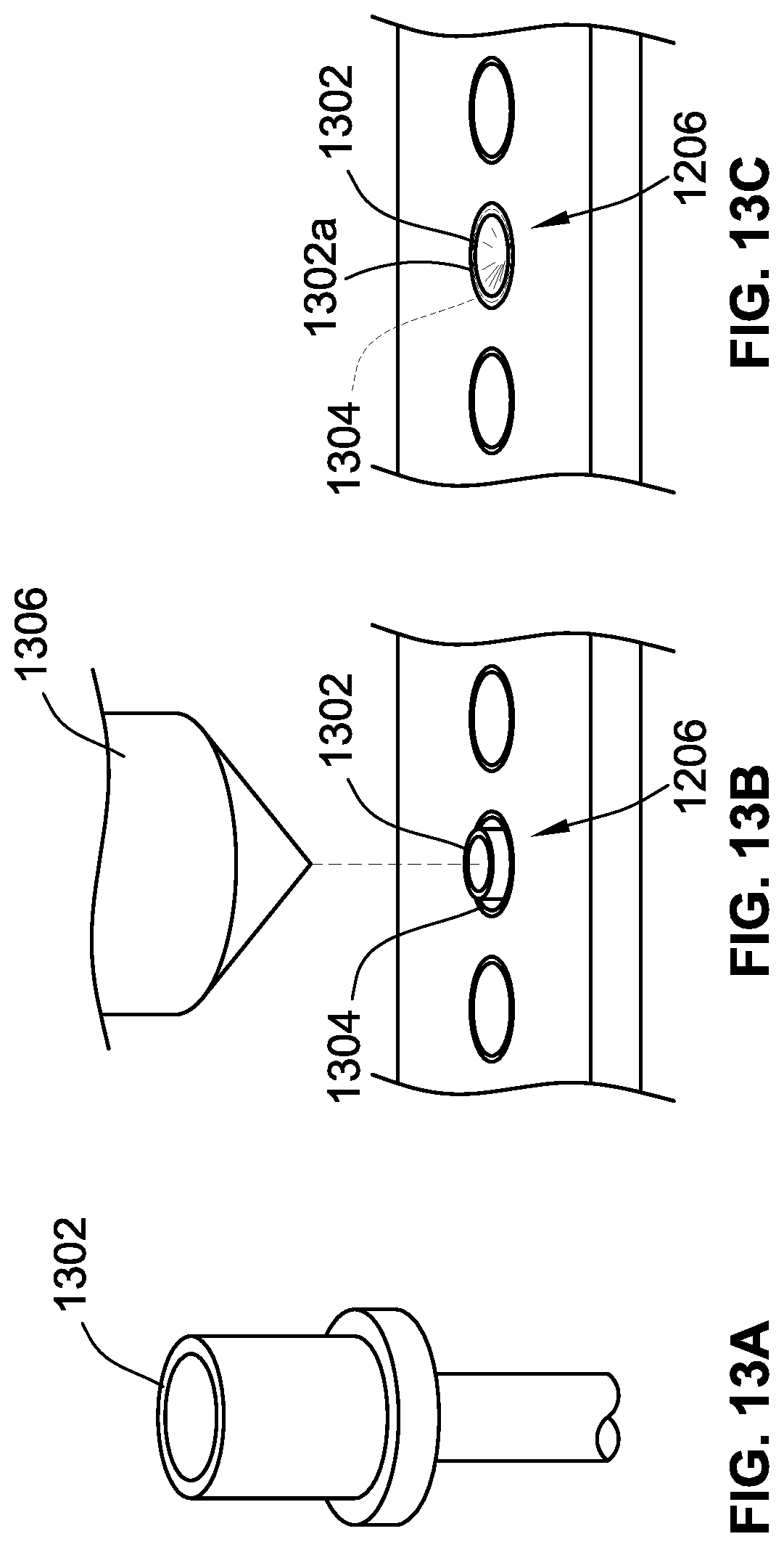
FIG. 13A shows an exemplary swage pin, in accord with some aspects of the present concepts;
FIG. 13B shows the exemplary swage pin of FIG. 13A inserted within a VIA, in accord with some aspects of the present concepts; and
FIG. 13C shows the exemplary swage pin of FIG. 13A fastened within the VIA of FIG. 13B by deformation, in accord with aspects of the present concepts.
The present disclosure is susceptible to various modifications and alternative forms, and some representative embodiments have been shown by way of example in the drawings and will be described in detail herein. It should be understood, however, that the invention is not intended to be limited to the particular forms disclosed. Rather, the disclosure is to cover all modifications, equivalents, and alternatives falling within the spirit and scope of the invention as defined by the appended claims.
DETAILED DESCRIPTION OF THE ILLUSTRATED EMBODIMENTS
This disclosure is susceptible of embodiment in many different forms. There are shown in the drawings, and will herein be described in detail, representative embodiments with the understanding that the present disclosure is to be considered as an exemplification of the principles of the present disclosure and is not intended to limit the broad aspects of the disclosure to the embodiments illustrated. To that extent, elements and limitations that are disclosed, for example, in the Abstract, Summary, and Detailed Description sections, but not explicitly set forth in the claims, should not be incorporated into the claims, singly or collectively, by implication, inference, or otherwise. For purposes of the present detailed description, unless specifically disclaimed: the singular includes the plural and vice versa; and the word "including" means "including without limitation." Moreover, words of approximation, such as "about," "almost," "substantially," "approximately," and the like, can be used herein in the sense of "at, near, or nearly at," or "within 3-5% of," or "within acceptable manufacturing tolerances," or any logical combination thereof, for example.
For purposes of illustration and to facilitate an understanding of the invention, the illustrative embodiments are described making reference to "top" and "bottom" in accordance with how the features are shown in the drawings. These reference designations are provided for convenience and the invention can be implemented with the features in other orientations, for example, with the positions reversed and device up-side down.
Flexible printed circuit board (FPCB) manufacturers typically use stiffeners on the backside (e.g., the side without components) or the component side of the FPCB assembly for both ease of assembly and reliability purposes. The stiffeners can be used to reinforce the FPCB assembly in the areas where electronic components are soldered to the FPCB to limit flexing that can cause the solder joints to break reducing the reliability of the assembly. According to the aspects of the present disclosure, the stiffeners can be conductive stiffeners and utilized to transmit thermal and/or electrical energy to components of the FPCB, rather than requiring externally attached electrodes. In accordance with some embodiments of the invention, the conductive stiffeners can function as electrodes for thermal and/or electrical measurements on a biological surface (e.g., tissue, such as skin) and provide mechanical stiffening of the FPCB assembly that can be incorporated into a conformable wearable device. Such conductive stiffeners can reduce the overall complexity and form factor of wearable devices by providing integrated permanent electrodes. The slender form factor of the wearable device can be achieved by fabricating and integrating positive, negative, and/or reference electrodes directly on the body-contacting surface of the FPCB assembly or the wearable device. The resulting conductive stiffener can be used to conduct electrical and/or thermal energy from biological tissue (e.g., skin, soft tissue, organs, etc.) to components mounted to the FPCB. The resulting conductive stiffener can also be used to increase the stiffness of at least a portion of the FPCB assembly. According to some embodiments, therefore, the conductive stiffener can have the same or similar shape and general dimensions as the FPCB assembly or a portion thereof.
The conductive stiffeners can be adhered and electrically and/or thermally connected to the surface (e.g., the backside or the component side) of the FPCB to allow for the collection of bio-potentials and/or bio-impedances such as electrooculography (EOG), electroencephalography (EEG), electromyogram (EMG), galvanic skin response (GSR), and electrocardiogram (ECG) signals by components of the FPCB assembly that forms part of the wearable device. The conductive stiffeners can also allow for the collection of temperature data through a thermally conductive medium and the ability to measure skin, body and/or tissue temperature without the need for auxiliary electrodes. The conductive stiffeners can also allow for the collection of bio-impedance data through the conductive skin contacting surfaces of the conductive stiffeners without the need for auxiliary electrodes.
FIGS. 1A-1D show various diagrammatic views of a conductive stiffener 100, in accord with aspects of the invention. Specifically, FIG. 1A shows a top view of the conductive stiffener 100. The dimensions (e.g., length and width) of the conductive stiffener 100 can correspond to the dimensions of the FPCB (or a portion thereof) to be stiffened. The conductive stiffener 100 can be covered with a conductive material 102 such that the top of the conductive stiffener 100 has top conductive layer 102a. According to some embodiments, the conductive material 102 can be any conductive material, such as any conducting metal. By way of example, and without limitation, the conductive material 102 can include copper, gold, silver, nickel, chrome, brass, bronze, lead free hot air solder, electroless nickel, immersion palladium, electroless palladium, immersion gold, electroless gold, electrolytic nickel, electrolytic gold, immersion tin, immersion silver, and various metal alloys. According to some embodiments, the conductive material 102 can be a ferrous material, such as stainless steel. According to the conductive material 102 being a ferrous material, the conductive stiffener 100 could also function as an alignment mechanism for applications associated with magnets. By way of example, and without limitation, the conductive stiffener 100 could function as an alignment mechanism for a wireless charger used in conjunction with the FPCB assembly.
The conductive stiffener 100 can also include one or more vertical interconnect access holes or VIAs 104 that extend through the conductive stiffener 100 to electrically and/or thermally connect the top conductive layer 102a with bottom conductive layer 102c. Although shown as being in the center of the conductive stiffener 100, the VIA(s) 104 can be located at other locations in the stiffener and can be positioned to align with conductive contact pads of the FPCB. The VIA 104 can be lined or filled with conductive material 102 forming a conductive tube or hollow column 102b, such as by plating or filling. In accordance with some embodiments, the VIA 104 can be surrounded by thermal reliefs 106, which are areas in the surface of the conductive stiffener 100 that do not include the conductive material 102. The thermal reliefs 106 aid in soldering the conductive stiffener 100 to a FPCB assembly.
FIG. 1B shows the bottom of the conductive stiffener 100, in accord with aspects of the present invention. Like the top, the bottom can be covered with the conductive material 102 to form a bottom conductive layer 102c. The bottom of the conductive stiffener 100 does not include the thermal reliefs 106, as shown; however, according to some embodiments, the bottom may also include thermal reliefs 106 depending on the intended placement of the conductive stiffener 100.
Referring to FIGS. 1C and 1D, FIG. 1C shows a cross-section view of the conductive stiffener 100 through the line 1C-1C in FIG. 1B, and FIG. 1D shows a cross-section view of the conductive stiffener 100 through line 1D-1D in FIG. 1A. As shown, the conductive stiffener 100 can include a top conductive layer 102a and a bottom conductive layer 102c. The conductive stiffener 100 can also include one or more conductive VIAs 104 that electrically and/or thermally connect the bottom conductive layer 102c to the top conductive layer 102a. The conductive stiffener 100 can include one or more non-conductive substrate layers 108a, 108b, between the top conductive layer 102a and bottom conductive layer 102c. The non-conductive substrate layers can be formed from a fiber reinforced material, such as, epoxy fiberglass (e.g., 370HR FR4 epoxy fiberglass sheet) or a FPCB non-conductive base material such as polyester, polyethylene terephthalate (PET), polyimide (PI), polyethylene napthalate (PEN), polyetherimide (PEI), fluropolymers (FEP) or a combination thereof.
As shown in FIGS. 1C and 1D, the conductive stiffener 100 can include one or more top non-conductive substrate layers 108a bonded or adhered to one or more bottom non-conductive substrate layers 108b. One or more adhesive layers 110 can be used to bond or adhere the adjacent non-conductive substrate layers 108a, 108b together.
In accordance with some embodiments, the top non-conductive substrate layer 108a and the bottom reinforced layer 108b can be formed of any type of non-conductive substrate material, such as any material used in the manufacture of a printed circuit board (PCB). According to some embodiments, the top non-conductive substrate layer 108a and the bottom non-conductive substrate layer 108b are formed of 370HR FR-4 glass-reinforced epoxy laminate sheets. However, the top non-conductive substrate layer 108a and the bottom non-conductive substrate layer 108b can be formed of other types of materials used in the PCB arts without departing from the spirit and scope of the present invention.
The adhesive layer 110 can be any suitable adhesive for adhering the top non-conductive substrate layer 108a and the bottom reinforced layer 108b together. According to some embodiments, the adhesive layer 110 can be, for example, an acrylic-based adhesive, such as a Pyralux.RTM. FRO200 and FRO300 adhesive, a polyester based adhesive, an epoxy based adhesive, or a polyimide based adhesive. However, the adhesive layer 110 can be formed of other types of adhesives used in the PCB arts without departing from the spirit and scope of the present disclosure.
While reference is made to top and bottom layers throughout the description for purposes illustrating the described examples of the embodiments of the invention, the conductive stiffener can be oriented and used in configurations where the top layer is below the bottom layer as well as in any angular orientation without departing from the scope and spirit of the invention.
According to some embodiments, the top conductive layer 102a and the bottom conductive layer 102b can be formed to a thickness of 0.0014'', the top non-conductive substrate layer 108a and the bottom non-conductive substrate layer 108b can formed to a thickness of 0.002'', and the adhesive layer 110 can be formed to a thickness of 0.002''. However, the layers can have varying and different thicknesses than the thicknesses disclosed herein without departing from the spirit and scope of the present disclosure. According to some embodiments, reducing the thickness of the various layers reduces the overall thickness of the FPCB assembly as well as the effectiveness as a stiffening component. In accordance with some embodiments, the stiffness can be increased by laminating two or more thin layers of non-conductive substrate material using an appropriate adhesive. Moreover, the thickness of the various layers can be selected such that the conductive stiffener 100 provides both thermal and electrical conductivity between the top conductive layer 102a and the bottom conductive layer 102c while minimizing the overall profile (e.g., thickness) of the conductive stiffener 100 and providing the desired amount stiffness to limit flexing of the attached PFCB.
Although illustrated a described above as including the top non-conductive substrate layer 108a, the adhesive layer 110, and the bottom non-conductive substrate layer 108b, the structure of the conductive stiffener 100 can vary without departing from the spirit and scope of the present disclosure. By way of example, and without limitation, according to some embodiments, the conductive stiffener 100 may instead include a single non-conductive substrate layer between the top conductive layer 102a and the bottom conductive layer 102c. The single non-conductive substrate layer can have the same thickness as, for example, the combination of the top non-conductive substrate layer 108a, the adhesive layer 110, and the bottom non-conductive substrate layer 108b, or may have a different thickness depending on, for example, the structural rigidity requirements of the resulting conductive stiffener 100.
Further, according to some embodiments, the top of the conductive stiffener 100 can exclude the top conductive layer 102a. Rather, the conductive material 102 can form only the bottom conductive layer 102c and the conductive tube or hollow column 102b within the VIA 104. With only the bottom conductive layer 102c and the conductive tube or hollow column 102b, the conductive stiffener 100 still provides electrical and thermal conductivity to the top of the conductive stiffener 100.
Referring to FIG. 2, FIG. 2 shows a flow diagram of a process 200 for making the conductive stiffener 100 illustrated in FIGS. 1A-1D, in accord with aspects of the invention. Although FIG. 2 illustrates and the following remarks describe the process 200 according to various acts in a specific sequence, the acts can be performed in varying sequences, and one or more acts can be added or omitted, without departing from the spirit and scope of the present disclosure.
Referring to step 202, the process 200 begins with adhering two non-conductive substrate sheets together with an adhesive to form a stiffener. The two non-conductive substrate sheets can be, for example, as described above with respect to the top non-conductive substrate sheet 108a and the bottom non-conductive substrate sheet 108b, the adhesive can be, for example, as described above with respect to the adhesive layer 110. In accordance with some embodiments, more than two non-conductive substrate sheets 108a, 108b . . . 108z can be adhered together using two or more adhesive layers 110.
At step 204, one or more holes can be formed through the stiffener to form a VIA. As stated above, a VIA can be formed anywhere on the stiffener; however, according to some embodiments, the VIA is formed in the middle of the stiffener. The VIA can be formed according to any conventional process for forming a VIA through the adhered non-conductive substrate layers, such as by drilling, punching, etching, etc.
At step 206, a conductive layer of conductive material can be formed on the exterior surfaces of the stiffener and lining the VIA. The conductive layer can be formed according to any conventional process, such as by plating, laminating, and/or using direct metallization, and can be formed to various thicknesses, such as 0.0007''. As described above, the conductive material used can be, for example, copper, gold, silver, nickel, chrome, brass, bronze, and metal alloys. In accordance with some embodiments, the conductive material can be applied on the top and bottom of the stiffener and through the VIA, thus electrically and/or thermally connecting the top and bottom surfaces of the stiffener through the VIA.
At step 208, the conductive stiffener can be further processed by forming a resist layer (e.g., a light sensitive etch resist layer or photoresist layer) on the conductive stiffener in a pattern that defines thermal reliefs surrounding the VIA on one side of the conductive stiffener (e.g., the top side). According to some embodiments, the resist layer can be formed 0.002'' thick to protect the conductive material that is intended to be left on the conductive stiffener after etching. The resist can be any suitable resist material used in the removal of the conductive material to form the thermal relief. By way of example, and with respect to copper as the conductive material, the resist material can be an ultraviolet light curing etch resistive material.
At step 210, the copper material exposed by the resist layer is then removed to form the thermal reliefs. According to some embodiments, and with respect to copper as the conductive material, the copper material can be removed by etching with ferric chloride, copper chloride or hydrochloric acid. After etching the conductive stiffener, the resist layer can be removed (e.g., by stripping) leaving the thermal relief pattern in the conductive material surrounding the VIA.
At step 212, after forming the thermal reliefs, additional conductive material can be formed on the remaining conductive material to thicken the conductive material surrounding the conductive stiffener. According to some embodiments, an additional 0.0007'' of conductive material, such as copper, can be formed above the remaining conductive material. According to some embodiments, the additional conductive material added in step 212 can be the same conductive material original formed on the stiffener. According to some embodiments, the additional conductive material can be a different conductive material, such as gold, silver, nickel, chrome, or a metal alloy.
According to some embodiments, at step 214, the conductive stiffener can be plated using an electroless nickel immersion gold process to protect the conductive layers on the top and bottom surfaces of the conductive stiffener. Plating can occur to only one side of the conductive stiffener, such as the side opposite from the FPCB, to provide for optimal electrode conductivity. Alternatively, both sides can be plated using the electroless nickel immersion gold process. However, step 214 can be omitted, or the conductive stiffener can be exposed to a different process to protect the conductive layers on the top and bottom surfaces. After step 214, the conductive stiffener is ready for application to a FPCB assembly.
Although the process 200 is described with respect to forming a single conductive stiffener, according to some embodiments, multiple conductive stiffeners can be formed simultaneously through a single process. By way of example, and without limitation, the dimensions of the two non-conductive substrate sheets in step 202 can be large enough to form multiple conductive stiffeners simultaneously. After forming the conductive stiffeners using appropriately large enough non-conductive substrate sheets, the two conductive stiffeners can be separated by cutting the two non-conductive substrate sheets into the respective conductive stiffeners.
According to some embodiments, prior to separating the conductive stiffeners, the two non-conductive substrate sheets can be plated with tin and patterned with an additional resist based on a pattern of the conductive material for each conductive stiffener. The tin and conductive material left unprotected by the resist can be removed, such as by submerging the structure in an alkaline solution. After removing the unprotected material, the resist and remaining tin can be removed, such as through a striping process. The conductive stiffeners can then be separated into the individual stiffeners.
Referring to FIG. 3, FIG. 3 shows a flow diagram of a process 300 for attaching a conductive stiffener to an FPCB assembly, in accord with aspects of the present concepts. Although FIG. 3 illustrates and the following remarks describe the process 300 according to various acts in a specific sequence, the acts can be performed in varying sequences, and one or more acts can be added or omitted, without departing from the spirit and scope of the present disclosure.
At step 302, an adhesive layer is applied to the top surface of the conductive stiffener around the VIA and the thermal reliefs. The adhesive material used to form the adhesive layer can be any suitable adhesive used in the PCB and FPCB arts, such as, for example, a Pyralux.RTM. FRO200 adhesive, polyimide based adhesive or epoxy based adhesive. The adhesive layer can be any suitable thickness to attach the conductive stiffener, such as, for example, 0.002'' thick. The adhesive layer can be formed around the VIA and the thermal reliefs of the VIA so as to provide room for solder to affix the conductive stiffener to the backside of a FPCB assembly.
At step 304, the conductive stiffener is adhered to the backside of the FPCB assembly by the adhesive layer. The adhesive layer at least partially attaches the conductive stiffener to the backside of the FPCB assembly. The conductive stiffener is adhered to the backside of the FPCB assembly such that the VIA of the conductive stiffener aligns with an electrical contact pad on the backside surface of the FPCB.
At step 306, the VIA is filled with solder (or another similar conductor) to complete the connection of the conductive stiffener to the backside of the FPCB assembly. The solder can be any suitable conductive material for attaching a stiffener to an FPCB assembly. Preferably the solder is a lead-free (e.g., tin or silver based solder) or other biocompatible solder to avoid incompatibility when the device is worn by a user. The conductive column and the solder within the VIA mechanically, electrically, and thermally connect the backside of the electrical component and the electrical contact pad to the conductive pad on the bottom surface of the conductive stiffener. Accordingly, the conductive stiffener provides both structural rigidity at specific positions of the FPCB assembly and thermal and electrical conductivity to electrical components of the FPCB assembly.
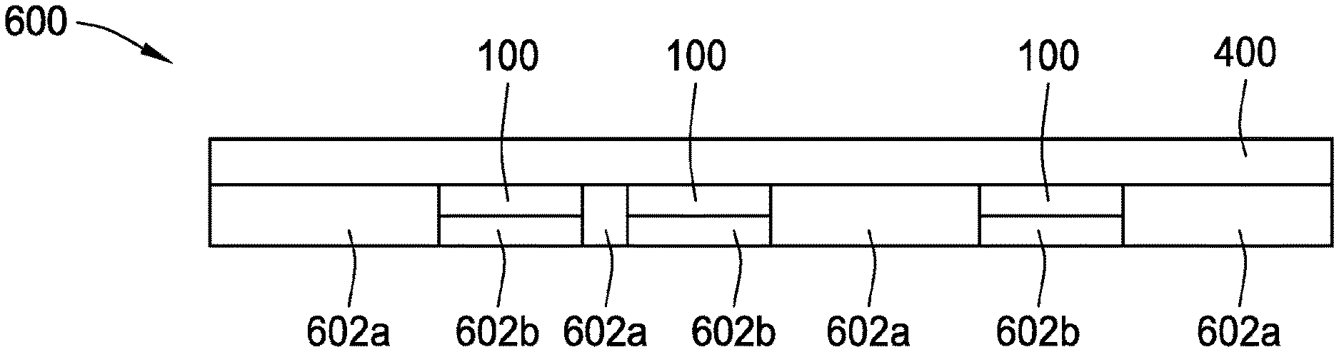
Referring to FIG. 4, FIG. 4 shows a perspective view of a backside of a FPCB assembly 400 with attached conductive stiffeners 100, in accord with aspects of the present concepts. As shown, the FPCB assembly 400 includes FPCB sections arranged in device islands 404 and surrounded by or encapsulated in a flexible polymer or elastomer substrate 402. The FPCB sections can be any conventional non-conductive or dielectric substrate for a FPCB, such as a polyimide and/or a silicone. The FPCB sections can include copper circuit traces and pads to facilitate attachment of electrical components, such as by soldering. By way of example, and without limitation, the electrical components can be any discrete operative device embedded in and/or affixed to the FPCB substrate 402, such as one or more microprocessors, microcontrollers, system on a chip devices, physical sensors (e.g., accelerometers, gyros, or inertial navigation sensors), biological and/or chemical sensors, active pixel sensors, amplifiers, analog-to-digital (A/D) converters, digital-to-analog (D/A) converters, optical sensors (e.g., photodiodes, photoresistors, CCD sensors), electro-mechanical transducers (e.g., MEMS sensors), piezo-electric sensors and actuators, light emitting diodes (LEDs), light emitting electronics, thermistors, thermocouples, memory devices, clock devices, active matrix switches, integrated circuits, resistors, capacitors, or other similar discrete operative devices. The FPCB assembly 400 can be constructed from two or more electrically interconnected device islands 404, each device island 404 including one or more electronic components embedded in or affixed to the FPCB. The device islands 404 can be interconnected by wires or interconnects 406. According to some embodiments, the interconnects 406 can be bendable and/or stretchable interconnects to accommodate the flexible, bendable, stretchable and conformal properties of the FPCB assembly 400, while also maintaining an electrical interconnection between two or more electrical components 404, such as two adjacent device islands 404, while in use.
The FPCB assembly 400 shown in FIG. 4 includes seven device islands 404, with the right most and two left most device islands 404 including conductive stiffeners 100 in accordance with some embodiments of the invention. Specifically, two conductive stiffeners 100 are aligned with and attached to the two leftmost device islands 404, and one larger conductive stiffener 100 is aligned with and attached to the rightmost device island 404. In accordance with some embodiments of the invention, the conductive stiffeners 100 can have the same shape as the device island 404 that the conductive stiffener 100 is attached is connected to. In accordance with some embodiments of the invention, the conductive stiffener 100 can larger or smaller (e.g., in one or two dimensions) than the device island 404 that it is attached to. Accordingly, the conductive stiffeners 100 provide stiffness as needed across the various FPCB sections and protect the device islands 404 from damage caused by bending of the FPCB assembly 400 (e.g., within certain limits). However, according to some embodiments, the conductive stiffener 100 can be slightly larger or slightly smaller than the device island 404 to provide more or less structural rigidity at the electrical component and, for example, to ensure complete overlap between the conductive stiffener 100 and the device island 404 during bending of the FPCB assembly 400.
FIG. 5 shows a cross section of a FPCB assembly 400 with the attached conductive stiffener 100 along the line 5-5 in FIG. 4, in accord with aspects of the present concepts. In accordance with some embodiments, the conductive stiffener 100 can include the top conductive layer 102b and the bottom conductive layer 102c, with the top non-conductive substrate layer 108a and the bottom non-conductive substrate layer 108b sandwiching the adhesive layer 110. The conductive stiffener 100 can also include the conductive tube or hollow column 102b within the VIA 104.
As shown, the conductive stiffener 100 is below a device island 404 of the FPCB assembly 400. The device island 404 can include one or more conductive contact pads 408, such an electrical and/or a thermal conductive contact pad. The conductive stiffener 100 can be affixed to the backside of the device island 404 so that the VIA 104 of the conductive stiffener 100 is aligned with the contact pad 408. The conductive stiffener 100 can further include solder 410 that fills the VIA and mechanically and electrically connects the conductive stiffener 100 to one or more contact pads 408 of device island 404. The thermal reliefs 106 (not shown in FIG. 5) allow the solder to fill the remaining void within the VIA 104 while reducing the thermal strain during soldering.
The conductive stiffener 100 provides structural rigidity to the FPCB assembly 400 at one or more device islands 404 and also thermally and/or electrically connects the device island 404 to the conductive stiffener 100. Accordingly, with the conductive stiffener 100 installed, the FPCB assembly 400, and particularly the device island 404 of the FPCB assembly 400, does not need to be connected to external electrodes. Rather, the conductive stiffeners 100 function as the external electrodes while providing a slim profile that provides little to no resistance to the conformability of the FPCB assembly 400.
The resulting encapsulated FPCB assembly 400 together with the conductive stiffener 100 can be referred to as a wearable device or a patch. The wearable device can be placed directly in contact with the user (e.g., the user's tissue, such as skin and generate mechanical, electrical and/or thermal measurements of the user using the electrical components of the FPCB assembly 400 and through the conductive stiffener 100. According to some embodiments, the FPCB assembly 400 and the conductive stiffeners 100 can be placed directly on the biological surface (e.g., a tissue of the user such as skin, endothelial tissue, and epithelial tissue). However, according to some embodiments, to increase the adhesion of the resulting wearable device to a biological surface (e.g., the skin of a user), all or a portion of the bottom surface of the FPCB assembly 400 and conductive stiffeners 100 can be coated with an adhesive layer.
FIG. 6 shows a cross-section view of a wearable device 600, in accord with aspects of the present concepts. The wearable device 600 includes the FPCB assembly 400 and multiple conductive stiffeners 100. The wearable device 600 can include an adhesive layer on one surface for attaching the device to a biological surface of the body. In accordance with some embodiments of the invention, the adhesive layer can be located on the bottom surface of the FPCB assembly 400 and surrounding the one or more conductive stiffeners 100 on three sides. The adhesive layer 602 can be any conventional adhesive layer used in adhering bandages and devices to the body, such as a silicone gel based adhesive or an acrylic based adhesive. In accordance with some embodiments, the adhesive layer 602 can be formed generally of a silicone adhesive. The adhesive layer 602 can include two different portions, a non-conductive adhesive portion 602a and a conductive portion 602b. The conductive portion 602b of the adhesive layer 602 permits electrical and/or thermal conduction through the adhesive layer 602. Accordingly, the conductive portions 602b can be positioned to align with the conductive stiffeners 100, and in some embodiments, the bottom conductive layers 102c of the conductive stiffeners 100, to allow thermal and electrical energy to pass through the adhesive layer 602 and reach the bottom conductive layers 102c of the conductive stiffeners 100. To isolate each respective conductive portion 602b, the adhesive layer 602 includes the non-conductive adhesive portions 602a that surround the conductive portions 602b. The non-conductive adhesive portions 602a are high impedance areas that prevent or substantially reduce the transmission of electrical energy and/or thermal energy there though. In accordance with some embodiments of the invention, the conductive
The conductive portions 602b of the adhesive layer 602 provide a thermal and/or electrical conductive interface, where needed, between the biological surface and conductive stiffeners 100. Because the adhesive layer 602 includes the conductive portions 602b, the wearable device 600 can measure thermal and/or electric (e.g., biopotential and bioimpedance) signals, such as EMG, ECG, heart rate, galvanic skin response, and/or ECG tracking, among others, while having adhesive properties to aid the wearable device 600 in remaining coupled to the user. Accordingly, the adhesive layer 602 aids the wearable device 600 in remaining coupled to the user during the various activities in which the wearable device 600 monitors the physical and biological signals of the user, such as during exercising, sleeping, etc. For example, the conformal and flexible nature of the wearable device 600 allow for it to be placed on various parts of the body to monitor, for example, muscle activities.
FIG. 7 shows an exploded perspective view of the wearable device 600 of FIG. 6, in accord with aspects of the present concepts, and FIG. 8 shows an isometric view of the wearable device 600 of FIGS. 6 and 7, in accord with aspects of the present concepts. As shown, the wearable device 600 includes the FPCB assembly 400, including the conductive stiffeners 100, on a top surface. The FPCB assembly 400 includes an adhesive layer 602. The adhesive layer 602 is generally comprised of the non-conductive adhesive portion 602a surrounding the conductive portions 602b. The conductive portions 602b align with the conductive stiffeners 100 to allow the conductive stiffeners 100 to receive electrical and/or thermal energy from a biological surface below the adhesive layer 602.
Although the conductive portions 602b of the adhesive layer 602 are shown as separate elements of the adhesive layer 602 relative to the non-conductive adhesive portions 602a, the conductive portions 602b can be integral with the non-conductive portions 602a. According to some embodiments, the conductive portions 602b can be integral with the non-conductive portions 602a by combining the same adhesive material (as the non-conductive portions 602a) with material additives that make the conductive adhesive portions 602b conductive. By way of example, and without limitation, the adhesive layer 602 can be formed of a silicone adhesive, and the conductive adhesive portions 602b can include additives that make the silicone within these portions conductive. According to some embodiments, the additives used to create the conductive portions 602b electrically and/or thermally conductive include silver (Ag), gold (Au), carbon, graphite, nickel/graphite, silver/silver chloride (Ag/AgCl) and other conductive material additives. Consequently, the non-conductive adhesive portions 602a of the adhesive layer 602 lack the conductive additives and provide good insulating properties. The conductive silicone used to form the conductive adhesive portions 602b can be integrated into the adhesive layer 602 according to various methodologies, to form integral or non-integral conductive adhesive portions 602b, such as by potting, insert molding, gluing, snapping, etc.
The conductive portions 602b provide a conductive path through the adhesive layer 602 that protects and isolates the underlying circuitry (e.g., electrical components 404 and interconnects 406) from the external environment. The conductive path only exists in selected areas that couple directly to the conductive stiffeners 100 on the backside of the FPCB assembly 400. According to some embodiments, the conductive portions 602b have volume resistivity in the range of 70 ohmcm to 0.003 ohmcm.
Although illustrated and described above with respect to the FPCB assembly 400 that includes the conductive stiffeners 100, according to some embodiments, the wearable device 600 of FIGS. 6-8 can exclude the conductive stiffeners 100. For example, depending on the specific application of the wearable device 600, the wearable device 600 may not require the additional stiffness provided by the conductive stiffeners 100. Accordingly, the conductive stiffeners 100 can be omitted. Instead, the conductive portions 602b of the adhesive layer 602 can interface directly with, for example, the various contact pads 408 or conductive surfaces of the device islands 404 of the FPCB assembly 400. The conductive portions 602b of the adhesive layer 602 can be configured (e.g, by selecting the appropriate thermally or electrically conductive material) to transmit the thermal and/or electrical energy directly to the contact pads 408 of the device islands 404.
Referring to FIGS. 9A and 9B, these figures show the ability of the wearable device 600 located at various positions on a user to detect physical and biological electrical signals during use, in accord with aspects of the present concepts. Referring to FIG. 9A, the signals shown represent a wearable device 600 adhered to the chest of the user with the ability to measure acceleration in three axes (e.g., x, y, and z axes) and ECG signals. Referring to FIG. 9B, the signals shown represent a wearable device 600 adhered to the leg of the user with the ability to measure acceleration in three axes (e.g., x, y, and z axes) and EMG signals. In both figures, the user was performing squats as exemplary activity during which the signals are measured. As shown in FIGS. 9A and 9B, the wearable devices 600 are able to detect the biological signals from the user through the conductive portions 602b.
As an alternative to the adhesive layer 602 being placed only on the backside of the FPCB assembly 400, according to some embodiments, the FPCB assembly 400, with or without the conductive stiffeners 100, can be encapsulated within an encapsulation material to entirely protect the electrical components. Encapsulating the FPCB assembly 400 (and the conductive stiffeners 100) within the encapsulation layer seals off and protects the components from the elements of the outside environment during use, such as water, sweat, dirt, etc. Further, according to some embodiments, an encapsulation layer allows the resulting wearable device (e.g., a patch) to satisfy certain national and/or international standards or tests with respect to, for example, electrical devices and, more specifically, medical electrical devices. By way of example, an encapsulation layer allows a device to pass International Protection Marking tests.
FIG. 10 shows a cross section view of a wearable device 1000, in accord with aspects of the present concepts. As shown, the wearable device 1000 includes the FPCB assembly 400 and multiple conductive stiffeners 100. However, according to some embodiments, and based on, for example, the application of the specific wearable device 1000, the wearable device 1000 may exclude the conductive stiffeners 100. As shown, the wearable device 1000 includes an encapsulation layer 1002 the entirely surrounds the FPCB assembly 400. A bottom surface 1002a of the encapsulation layer 1002 can include an adhesive layer, similar to the adhesive layer 602 discussed above, but that the encapsulation layer also is above the FPCB assembly 400. Accordingly, the encapsulation layer 1002 can be formed of various conformable materials used in encapsulating electronics, such a silicones. The encapsulation layer 1002 can be non-conductive to prevent, for example, electrical signals from short circuiting or affecting measurements of the electrical components of the FPCB assembly 400. However, the encapsulation layer 1002 includes conductive portions 1004 that transmit thermal and/or electrical energy through the encapsulation layer 1002. The conductive portions 1004 can be similar in construction and function as the conductive 602b of the adhesive layer 602, and similarly, the conductive portions 1004 can be aligned with the conductive stiffeners 100 or contact pads 408 of the FPCB assembly 400.
By encapsulating the FPCB assembly 400 within the encapsulation layer 1002, the wearable device 1000 permits, for example, the monitoring of physical and biological signals, such as EMG, ECG, etc., underwater. Moreover, by having the conductive portions 1004 integrated into the encapsulation layer 1002, and below the conductive stiffeners 100 or contact pads 408 of the device islands 404, the wearable device 1000 functions as an entirely integrated monitoring device that does not require, for example, additional electrodes tethered by wires to the FPCB assembly 400.
As disclosed above, and according to some embodiments, the adhesive layer 602 and the encapsulation layer 1002 can be generally applied to the FPCB assembly 400 such that, for example, the interface between the adhesive layer 602 or the encapsulation layer 1002 and the FPCB assembly 400, or components thereof, is a planar or smooth interface. However, according to some embodiments, features can be formed into the FPCB assembly 400 and/or the conductive stiffeners 100 to provide a more mechanically stable interface for the adhesive layer 602 or the encapsulation layer 1002.
Accordingly, FIG. 11 shows a bottom view of features 1102 formed on a substrate 1100 to provide an improved interface, in accord with aspects of the present concepts. Specifically, FIG. 11 shows a substrate 1100. The substrate 1100 can generally refer to a conductive stiffener 100, a device island 404 of the FPCB assembly 400, or the entire FPCB assembly 400. Thus, the substrate 1100 includes a surface that interfaces with the adhesive layer 602 or the encapsulation layer 1002.
To improve adhesion of, for example, the conductive adhesive portions 602b and the conductive portion 1004, the substrate 1100 can includes features 1102. According to some embodiments, the features 1102 can be VIAs formed in the substrate 1100. According to some embodiments, the VIAs can extend entirely through the substrate 1100, or may extend partially into the substrate 1100. The adhesive layer 602 or the encapsulation layer 1002 at least partially fills the VIAs to provide a larger contact area and greater mechanical adhesion to the substrate 1100. Thus, the features 1102 as VIAs provide some additional mechanical grip for the adhesive layer 602 or the encapsulation layer 1002 such that these layers do not have to solely rely on adhesion to a planar surface. Accordingly, the features 1102 applied to the FPCB assembly 400 and/or the conductive stiffeners 100 provide a better adhesive interface with the adhesive layer 602 and the encapsulation layer 1002 to improve the mechanical grip between the two different layers.
As alternatives to VIAs, the features 1102 may be any other type of protuberance and/or indentation on the substrate 1100 that alters the smooth surface of the substrate 1100 to something other than substantially smooth or planar. By way of example, and without limitation, according to some embodiments, the features 1102 can be pad rings that protrude beyond the surface of the substrate 1100. Alternatively, the features 1102 can be a combination of VIAs and pad rings surrounding the VIAs, such that the adhesive layer 602 or the encapsulation layer 1002 both extends into the VIAs and extends over the pads rings. Further, although a specific arrangement and number of features are illustrated in FIG. 11, the number and arrangement of the features 1102 can vary without departing from the spirit and scope of the present disclosure.
In addition or in the alternative to forming features in or on the FPCB assembly 400 of the conductive stiffeners 100 to improve adhesion with the adhesive layer 602 or the encapsulation layer 1002, according to some embodiments, the configuration of the FPCB assembly 400 can be changed.
FIG. 12 shows an exemplary configuration of a FPCB assembly 400 to improve mechanical adhesion to the FPCB assembly 400, in accord with some aspects of the present concepts. FIG. 12 includes a FPCB assembly 400 that has its ends 1202a and 1202b folded to form pockets 1204a and 1204b between the folded ends 1202a and 1202b and the main body 1200 of the FPCB assembly 400. The pockets 1204a and 1204b sandwich the material of the adhesive layer 602 or the encapsulation layer 1002 between the pockets 1204a and 1204b and the main body 1202. By sandwiching the material, the configuration of the FPCB assembly 400 provides additional mechanical strength and/or resistance to the adhesive layer 602 or the encapsulation layer 1002 from being removed from the FPCB assembly 400.
According to some embodiments, and as illustrated in FIG. 12, the ends 1202a and 1202b can also include VIAs 1206. The VIAs 1206 can be through only the FPCB assembly 400, or the VIAs 1206 can be through the FPCB assembly 400 and conductive stiffeners 100 located at the ends 1202a and 1202b of the FPCB assembly 400. When the pockets 1204a and 1204b are filled with the material of the adhesive layer 602 or the encapsulation layer 1002, the material flows from inside the pockets 1204a and 1204b and through the VIAs 1206 to outside of the pockets 1204a and 1204b. The material through the VIAs 1206 provides additional mechanical contact with FPCB assembly 400 such that the material of the adhesive layer 602 or the encapsulation layer 1002 does not rely solely on its adhesion to the planar surface of the FPCB assembly 400. Additionally, the VIAs 1206 can be electrically connected to electrical components 404 of the FPCB assembly 400, and the material that flows through the VIAs 1206 can be the conductive material that forms the conductive adhesive portions 602b of the adhesive layer 602 or the conductive portion 1004 of the encapsulation layer 1002. Thus, the point of mechanical contact can also be a point of electrical contact between the adhesive layer 602/encapsulation layer 1002 and the FPCB assembly 400.
The adhesive layer 602 or the encapsulation layer 1002 under the main body 1200 can be filled to form a substantially planer surface of the adhesive layer 602 or the encapsulation layer 1002 on the backside of the FPCB assembly 400 to form the wearable device 600 or 1000. Thus, the surface that contacts the biological surface can still be substantially planar. Further, although both ends 1202a and 1202b are shown in FIG. 12 as folded to form the pockets 1204a and 1204, according to some embodiments, only one end (e.g., 1202a or 1202b) can be folded to form a pocket (e.g., 1204a or 1204b) in the FPCB assembly 400.
FIGS. 13A-13C show an exemplary and optional configuration of the VIAs 1206 for electrical and mechanical contact, in accord with some aspects of the present concepts. Specifically, electrical and mechanical contact can be further improved by application of an electrically conductive insert within the VIA 1206. Such an insert can be, for example, an electrically conductive rivet or swage pin 1302 (FIGS. 13A-13C). The electrically conductive insert can interface with a conductive ring 1304 (FIGS. 13B and 13C) around the VIA 1206 at the surface. Application of the electrically conductive insert into the VIA 1206 can cause the insert to contact the conductive ring 1304. In the example of the electrically conductive rivet or swage pin 1302 as the insert, the rivet or swage pin 1302 can be applied using an arbor press (not shown) and swage punch 1306 (FIG. 13B) through the VIA 1206, with the resulting flared portion 1302a of the rivet or swage pin 1302 contacting the conductive ring 1304 (FIGS. 13B and 13C) to provide electrical contact to the rivet or swage pin 1302 after swaging.
The various wearable devices disclosed above are fully-functional skin-mountable devices with conductive stiffeners functioning as integrated single-channel or multi-channel electrodes. The conductive stiffeners also provide mechanical stability for the electrical components on the top side of the FPCB. The arrangement of the conductive stiffeners and the adhesive layer or encapsulation layer reduces the overall thickness of the resulting skin-mountable wearable device, while also simplifying the manufacturing process in which electrode functionality is required.
Including conductive stiffeners on the backside surface of FPCB and aligned with contact pads of electronic components of the FPCB provides both mechanical and electrical functionalities and benefits. For example, the conductive stiffeners provide mechanical stability to the backside of surface mounted or embedded electronic components in FPCB for mechanical reliability purposes. Further, the conductive stiffeners provide an electrically conductive medium on the backside of FPCB with conductive adhesive contact directly with skin or any other soft biological tissue. The conductive stiffeners also provide a thermally conductive medium on the backside of the FPCB for thermal relief and/or temperature sensing of the surface mounted or embedded electronic components.
According to some embodiments, combining the conductive stiffener with the FPCB combines two elements and reduces the total number of parts and instructions for use that are required to measure, for example, electrical activity from a biological surface. The reduction in the number of components and complexity manifest in less noisy signal quality because of, for example, the reduced electrical length between the sensor (e.g., the bottom conductive layer of the conductive stiffener) and the receiver (e.g., the electrical component). The reduced electrical length eliminates sources of noise, such as 60 Hz noise from power lines and motion artifacts from movement.
In addition to sensing, the conductive stiffeners also can provide sites for active alternating current (AC) and/or direct current (DC) stimuli to be applied to the skin, peripheral nerves, or any other soft biological site. The conductive stiffeners also allow for charging a skin-mounted wearable device using the conductive surfaces as the charging interfaces.
While particular embodiments and applications of the present disclosure have been illustrated and described, it is to be understood that the present disclosure is not limited to the precise construction and compositions disclosed herein and that various modifications, changes, and variations can be apparent from the foregoing descriptions without departing from the spirit and scope of the invention as defined in the appended claims.
* * * * *
References
D00000
D00001
D00002
D00003
D00004
D00005
D00006
D00007
D00008
D00009
D00010
XML
uspto.report is an independent third-party trademark research tool that is not affiliated, endorsed, or sponsored by the United States Patent and Trademark Office (USPTO) or any other governmental organization. The information provided by uspto.report is based on publicly available data at the time of writing and is intended for informational purposes only.
While we strive to provide accurate and up-to-date information, we do not guarantee the accuracy, completeness, reliability, or suitability of the information displayed on this site. The use of this site is at your own risk. Any reliance you place on such information is therefore strictly at your own risk.
All official trademark data, including owner information, should be verified by visiting the official USPTO website at www.uspto.gov. This site is not intended to replace professional legal advice and should not be used as a substitute for consulting with a legal professional who is knowledgeable about trademark law.