LED packages with chips having insulated surfaces
Lowes , et al.
U.S. patent number 10,622,522 [Application Number 14/478,571] was granted by the patent office on 2020-04-14 for led packages with chips having insulated surfaces. This patent grant is currently assigned to Theodore Lowes. The grantee listed for this patent is CREE, INC.. Invention is credited to Chandan Bhat, Bernd Keller, Theodore Lowes, Kurt W. Wilcox.


View All Diagrams
| United States Patent | 10,622,522 |
| Lowes , et al. | April 14, 2020 |
LED packages with chips having insulated surfaces
Abstract
Emitter packages are disclosed that can include an insulating layer covering the emitter, such as between the emitter's primary emission surface and a lens or encapsulant. The packages can comprise a submount with an emitter flip-chip mounted such that the diode region is between the emitter's non-insulating and/or conductive substrate and the submount. The submount can then be covered with a thin insulating layer. The same or another insulating layer can cover other electrically active surfaces on the submount. By insulating the electrically active surfaces of the emitter and, in some embodiments, other electrically active surfaces, the package can meet UL8750 class 4 enclosure standards even if it does not meet the lens adhesion criteria. This can enable the use of cheaper and/or more optically efficient materials at the fixture level, since the package itself meets class 4 standards.
| Inventors: | Lowes; Theodore (Lompoc, CA), Wilcox; Kurt W. (Libertyville, IL), Keller; Bernd (Santa Barbara, CA), Bhat; Chandan (Goleta, CA) | ||||||||||
|---|---|---|---|---|---|---|---|---|---|---|---|
| Applicant: |
|
||||||||||
| Assignee: | Lowes; Theodore (Durham,
NC) |
||||||||||
| Family ID: | 55438306 | ||||||||||
| Appl. No.: | 14/478,571 | ||||||||||
| Filed: | September 5, 2014 |
Prior Publication Data
| Document Identifier | Publication Date | |
|---|---|---|
| US 20160072022 A1 | Mar 10, 2016 | |
| Current U.S. Class: | 1/1 |
| Current CPC Class: | H01L 33/44 (20130101); H01L 33/486 (20130101); H01L 2224/32225 (20130101); H01L 2224/48227 (20130101); H01L 33/505 (20130101); H01L 2924/181 (20130101); H01L 2224/49107 (20130101); H01L 2224/73265 (20130101); H01L 2924/181 (20130101); H01L 2924/00012 (20130101); H01L 2224/73265 (20130101); H01L 2224/32225 (20130101); H01L 2224/48227 (20130101); H01L 2924/00 (20130101) |
| Current International Class: | H01L 33/48 (20100101); H01L 33/44 (20100101); H01L 33/50 (20100101) |
References Cited [Referenced By]
U.S. Patent Documents
| 3760237 | September 1973 | Jaffe |
| 4322735 | March 1982 | Tetsuo et al. |
| 4511425 | April 1985 | Boyd |
| 4972089 | November 1990 | Stevenson |
| 5042048 | August 1991 | Meyer |
| 5122943 | June 1992 | Pugh |
| 5130761 | July 1992 | Toshiaki |
| 5381599 | January 1995 | Hall |
| 5790298 | August 1998 | Tonar |
| 5813753 | September 1998 | Vriens et al. |
| 5942770 | August 1999 | Ishinaga et al. |
| 5959316 | September 1999 | Lowery |
| 6061160 | May 2000 | Maruyama |
| 6183100 | February 2001 | Suckow et al. |
| 6259608 | July 2001 | Berardinelli et al. |
| 6296367 | October 2001 | Parsons et al. |
| 6345903 | February 2002 | Koike et al. |
| 6359236 | March 2002 | DiStefano et al. |
| 6376902 | April 2002 | Arndt |
| 6392294 | May 2002 | Yamaguchi |
| 6447124 | September 2002 | Fletcher et al. |
| 6454437 | September 2002 | Kelly |
| 6536913 | March 2003 | Yajima et al. |
| 6621210 | September 2003 | Kato et al. |
| 6700136 | March 2004 | Guida |
| 6707069 | March 2004 | Song et al. |
| 6710373 | March 2004 | Wang |
| 6717353 | April 2004 | Mueller et al. |
| 6759733 | July 2004 | Arndt |
| 6765235 | July 2004 | Taninaka et al. |
| 6770498 | August 2004 | Hsu |
| 6858879 | February 2005 | Waitl et al. |
| 6964877 | November 2005 | Chen et al. |
| 6995510 | February 2006 | Murakami |
| D517025 | March 2006 | Asakawa |
| 7009285 | March 2006 | Su et al. |
| 7009627 | March 2006 | Abe et al. |
| 7021797 | April 2006 | Minano et al. |
| 7066626 | June 2006 | Omata |
| 7119422 | October 2006 | Chin |
| 7187009 | March 2007 | Fukasawa et al. |
| 7224000 | May 2007 | Aanegola et al. |
| 7244965 | July 2007 | Andrews et al. |
| 7282740 | October 2007 | Chikugawa et al. |
| 7282785 | October 2007 | Yoshida |
| 7285802 | October 2007 | Ouderkirk et al. |
| 7286926 | October 2007 | Gotoh et al. |
| 7303315 | December 2007 | Ouderkirk et al. |
| D572210 | July 2008 | Lee |
| D572670 | July 2008 | Ono et al. |
| D576574 | September 2008 | Kobayakawa |
| 7429757 | September 2008 | Oyama et al. |
| 7579628 | August 2009 | Inoguchi |
| 7622795 | November 2009 | Chiang |
| 7635915 | December 2009 | Xie et al. |
| 7692206 | April 2010 | Loh |
| 7777412 | August 2010 | Pang |
| 7875899 | January 2011 | Yasuda |
| 7923831 | April 2011 | Ng |
| 7932111 | April 2011 | Edmond |
| 7939848 | May 2011 | Kim |
| 8217414 | July 2012 | Hayashi |
| 2002/0030194 | March 2002 | Camras et al. |
| 2002/0057057 | May 2002 | Sorg |
| 2002/0061174 | May 2002 | Hurt et al. |
| 2002/0066905 | June 2002 | Wang |
| 2002/0123164 | September 2002 | Slater, Jr. |
| 2002/0156187 | October 2002 | Greene |
| 2002/0171087 | November 2002 | Krames et al. |
| 2003/0116769 | June 2003 | Song et al. |
| 2003/0121511 | July 2003 | Hashimura et al. |
| 2003/0160256 | August 2003 | Durocher et al. |
| 2003/0183852 | October 2003 | Takenaka |
| 2004/0016938 | January 2004 | Baretz et al. |
| 2004/0037076 | February 2004 | Katoh et al. |
| 2004/0041222 | March 2004 | Loh |
| 2004/0047151 | March 2004 | Bogner et al. |
| 2004/0079957 | April 2004 | Andrews et al. |
| 2004/0080939 | April 2004 | Braddell et al. |
| 2004/0090174 | May 2004 | Tasch et al. |
| 2004/0126913 | July 2004 | Loh |
| 2004/0201028 | October 2004 | Waitl |
| 2004/0207999 | October 2004 | Castillo et al. |
| 2004/0227149 | November 2004 | Ibbetson |
| 2004/0238930 | December 2004 | Arndt |
| 2004/0256706 | December 2004 | Nakashima |
| 2005/0072981 | April 2005 | Suenaga |
| 2005/0077535 | April 2005 | Li |
| 2005/0082574 | April 2005 | Tasch et al. |
| 2005/0110033 | May 2005 | Heremans et al. |
| 2005/0152127 | July 2005 | Kamiya et al. |
| 2005/0156187 | July 2005 | Isokawa |
| 2005/0179041 | August 2005 | Harbers et al. |
| 2005/0179376 | August 2005 | Fung et al. |
| 2005/0199899 | September 2005 | Lin et al. |
| 2005/0231983 | October 2005 | Dahm |
| 2005/0253130 | November 2005 | Tsutsumi et al. |
| 2006/0049477 | March 2006 | Arndt |
| 2006/0054912 | March 2006 | Murakami et al. |
| 2006/0060867 | March 2006 | Suehirom |
| 2006/0091406 | May 2006 | Kaneko |
| 2006/0102917 | May 2006 | Oyama |
| 2006/0105478 | May 2006 | Camras et al. |
| 2006/0105485 | May 2006 | Basin |
| 2006/0108594 | May 2006 | Iwasaki et al. |
| 2006/0131591 | June 2006 | Sumitani |
| 2006/0151809 | July 2006 | Isokawa |
| 2006/0180925 | August 2006 | Lee |
| 2006/0186428 | August 2006 | Tan |
| 2006/0220046 | October 2006 | Yu et al. |
| 2006/0267031 | November 2006 | Tasch et al. |
| 2006/0267042 | November 2006 | Izuno et al. |
| 2006/0278882 | December 2006 | Leung et al. |
| 2006/0284207 | December 2006 | Park |
| 2006/0291185 | December 2006 | Atsushi |
| 2007/0050530 | March 2007 | Seo |
| 2007/0096139 | May 2007 | Schultz |
| 2007/0145401 | June 2007 | Masahiro |
| 2007/0176193 | August 2007 | Nagai |
| 2007/0215998 | September 2007 | Hu |
| 2007/0221928 | September 2007 | Lee |
| 2007/0241357 | October 2007 | Yan |
| 2007/0262328 | November 2007 | Bando |
| 2007/0269586 | November 2007 | Leatherdale |
| 2007/0294975 | December 2007 | Nadar et al. |
| 2007/0295975 | December 2007 | Omae |
| 2008/0026498 | January 2008 | Tarsa et al. |
| 2008/0032142 | February 2008 | Tasumi |
| 2008/0041625 | February 2008 | Cheong |
| 2008/0074032 | March 2008 | Yano et al. |
| 2008/0093606 | April 2008 | Yu-Tang et al. |
| 2008/0149960 | June 2008 | Amo |
| 2008/0170391 | July 2008 | Norfidathul |
| 2008/0191610 | August 2008 | Oshio |
| 2008/0198594 | August 2008 | Lee |
| 2008/0230790 | September 2008 | Seko et al. |
| 2008/0258156 | October 2008 | Hata |
| 2008/0258168 | October 2008 | Loh et al. |
| 2008/0296590 | December 2008 | Ng |
| 2009/0050907 | February 2009 | Yuan et al. |
| 2009/0050924 | February 2009 | Edmond |
| 2009/0057708 | March 2009 | Abdul Karim et al. |
| 2009/0072251 | March 2009 | Chan et al. |
| 2009/0091258 | April 2009 | Heuser |
| 2009/0095966 | April 2009 | Keller et al. |
| 2009/0108281 | April 2009 | Keller |
| 2009/0129085 | May 2009 | Aizar et al. |
| 2009/0283781 | November 2009 | Chan et al. |
| 2009/0283787 | November 2009 | Donofrio |
| 2010/0044735 | February 2010 | Oyamada |
| 2010/0103660 | April 2010 | Van de Ven et al. |
| 2010/0155763 | June 2010 | Donofrio |
| 2010/0155769 | June 2010 | Lin |
| 2010/0181594 | July 2010 | Lin |
| 2010/0193822 | August 2010 | Inobe et al. |
| 2010/0321920 | December 2010 | Wu |
| 2011/0049545 | March 2011 | Basin et al. |
| 2011/0108874 | May 2011 | Chu |
| 2011/0121345 | May 2011 | Andrews et al. |
| 2011/0147778 | June 2011 | Ichikawa |
| 2011/0186880 | August 2011 | Kohler et al. |
| 2011/0193118 | August 2011 | Oshima |
| 2011/0220920 | September 2011 | Collins |
| 2011/0278617 | November 2011 | Lee |
| 2012/0032355 | February 2012 | Wang |
| 2012/0146066 | June 2012 | Tischler |
| 2012/0193649 | August 2012 | Donofrio |
| 2012/0193660 | August 2012 | Donofrio |
| 2012/0193661 | August 2012 | Emerson |
| 2012/0235199 | September 2012 | Andrews et al. |
| 2012/0257386 | October 2012 | Harbers et al. |
| 2012/0268957 | October 2012 | Premysler |
| 2012/0305949 | December 2012 | Donofrio |
| 2013/0056774 | March 2013 | Hong et al. |
| 2013/0063024 | March 2013 | Wada |
| 2013/0328074 | December 2013 | Lowes |
| 2013/0337591 | December 2013 | Chen |
| 2014/0027795 | January 2014 | Reiherzer |
| 2014/0034986 | February 2014 | Bradley Jr. |
| 2014/0175473 | June 2014 | Donofrio et al. |
| 2015/0004726 | January 2015 | Konishi |
| 2015/0137162 | May 2015 | Sabathil |
| 1977399 | Jun 2007 | CH | |||
| 1274906 | Nov 2000 | CN | |||
| 1417868 | May 2003 | CN | |||
| 2549313 | May 2003 | CN | |||
| 2617039 | May 2004 | CN | |||
| 1581527 | Feb 2005 | CN | |||
| 1591924 | Mar 2005 | CN | |||
| 1679168 | Oct 2005 | CN | |||
| 1720608 | Jan 2006 | CN | |||
| 1744335 | Mar 2006 | CN | |||
| 1874011 | Dec 2006 | CN | |||
| 1913135 | Feb 2007 | CN | |||
| 101005109 | Jul 2007 | CN | |||
| 101013689 | Aug 2007 | CN | |||
| 101360368 | Feb 2009 | CN | |||
| 202007012162 | Apr 2008 | DE | |||
| 102013215650 | Mar 2015 | DE | |||
| 0684648 | Nov 1995 | EP | |||
| 1005085 | May 2000 | EP | |||
| 1005085 | Dec 2000 | EP | |||
| 1187226 | Mar 2002 | EP | |||
| 1187227 | Mar 2002 | EP | |||
| 1187228 | Mar 2002 | EP | |||
| 1418630 | May 2004 | EP | |||
| 1521313 | Apr 2005 | EP | |||
| 1538680 | Jun 2005 | EP | |||
| 1653254 | May 2006 | EP | |||
| 1693904 | Aug 2006 | EP | |||
| 1850399 | Oct 2007 | EP | |||
| 1864780 | Dec 2007 | EP | |||
| 1953834 | Aug 2008 | EP | |||
| 2420221 | Dec 2004 | GB | |||
| 2458972 | Oct 2009 | GB | |||
| 2466633 | Jul 2010 | GB | |||
| 53118019 | Oct 1978 | JP | |||
| S53118019 | Oct 1978 | JP | |||
| S53126570 | Oct 1978 | JP | |||
| 5927559 | Feb 1984 | JP | |||
| 59027559 | Feb 1984 | JP | |||
| 6148951 | Mar 1986 | JP | |||
| 6148951 | Mar 1986 | JP | |||
| 61048951 | Mar 1986 | JP | |||
| S62160564 | Mar 1986 | JP | |||
| 62047156 | Feb 1987 | JP | |||
| 62140758 | Sep 1987 | JP | |||
| 038459 | Jan 1991 | JP | |||
| 07202271 | Aug 1995 | JP | |||
| 7202271 | Aug 1995 | JP | |||
| 07231120 | Aug 1995 | JP | |||
| 08032120 | Feb 1996 | JP | |||
| 8139257 | May 1996 | JP | |||
| 10135492 | May 1998 | JP | |||
| 10321909 | Dec 1998 | JP | |||
| 11008405 | Jan 1999 | JP | |||
| 11054802 | Feb 1999 | JP | |||
| 11150306 | Jun 1999 | JP | |||
| 11261113 | Sep 1999 | JP | |||
| 2000188358 | Jul 2000 | JP | |||
| 2000223751 | Aug 2000 | JP | |||
| 2000261041 | Sep 2000 | JP | |||
| 2001168400 | Jun 2001 | JP | |||
| 2001237463 | Aug 2001 | JP | |||
| 2001518692 | Oct 2001 | JP | |||
| 2002009217 | Jan 2002 | JP | |||
| 2002223005 | Aug 2002 | JP | |||
| 2002280479 | Sep 2002 | JP | |||
| 2002374005 | Dec 2002 | JP | |||
| 2003007946 | Jan 2003 | JP | |||
| 2003197974 | Jul 2003 | JP | |||
| 2003218405 | Jul 2003 | JP | |||
| 2003264267 | Sep 2003 | JP | |||
| 2003318449 | Nov 2003 | JP | |||
| 2003324214 | Nov 2003 | JP | |||
| 2004022862 | Jan 2004 | JP | |||
| 2004056075 | Feb 2004 | JP | |||
| 2004103775 | Feb 2004 | JP | |||
| 2004507114 | Mar 2004 | JP | |||
| 2004111937 | Apr 2004 | JP | |||
| 2004146815 | May 2004 | JP | |||
| 2004200236 | Jul 2004 | JP | |||
| 2004228387 | Aug 2004 | JP | |||
| 2004327955 | Nov 2004 | JP | |||
| 2004335740 | Nov 2004 | JP | |||
| 2004335880 | Nov 2004 | JP | |||
| 2004342870 | Dec 2004 | JP | |||
| 200519838 | Jan 2005 | JP | |||
| 2005019838 | Jan 2005 | JP | |||
| 2005045199 | Feb 2005 | JP | |||
| 2005079167 | Mar 2005 | JP | |||
| 2005150624 | Jun 2005 | JP | |||
| 2005223222 | Aug 2005 | JP | |||
| 2005259754 | Sep 2005 | JP | |||
| 2005259972 | Sep 2005 | JP | |||
| 2005310935 | Nov 2005 | JP | |||
| 2005539386 | Dec 2005 | JP | |||
| 2006508537 | Mar 2006 | JP | |||
| 2006509372 | Mar 2006 | JP | |||
| 2006108517 | Apr 2006 | JP | |||
| 2006119357 | May 2006 | JP | |||
| 2006179520 | Jul 2006 | JP | |||
| 2006253689 | Sep 2006 | JP | |||
| 2006324589 | Nov 2006 | JP | |||
| 2006525679 | Nov 2006 | JP | |||
| 2006332234 | Dec 2006 | JP | |||
| 2006344692 | Dec 2006 | JP | |||
| 200795797 | Apr 2007 | JP | |||
| 2007094088 | Apr 2007 | JP | |||
| 2007109836 | Apr 2007 | JP | |||
| 2007509505 | Apr 2007 | JP | |||
| 2007142281 | Jun 2007 | JP | |||
| 2007165029 | Jun 2007 | JP | |||
| 2007165840 | Jun 2007 | JP | |||
| 2007184542 | Jul 2007 | JP | |||
| 2007243226 | Sep 2007 | JP | |||
| 2007273763 | Oct 2007 | JP | |||
| 2007281323 | Oct 2007 | JP | |||
| 2007317896 | Dec 2007 | JP | |||
| 2007329516 | Dec 2007 | JP | |||
| 2008518461 | May 2008 | JP | |||
| 2008521236 | Jun 2008 | JP | |||
| 2000223752 | Aug 2008 | JP | |||
| H11054802 | Mar 2011 | JP | |||
| 2251761 | Feb 2005 | RU | |||
| WO 9931737 | Jun 1999 | WO | |||
| WO 0217405 | Feb 2002 | WO | |||
| WO 03049204 | Jun 2003 | WO | |||
| WO 2004027882 | Jan 2004 | WO | |||
| WO 200403660 | Apr 2004 | WO | |||
| WO 2004036660 | Apr 2004 | WO | |||
| WO 2004036660 | Apr 2004 | WO | |||
| WO 04044877 | May 2004 | WO | |||
| WO 2004053933 | Jun 2004 | WO | |||
| WO 05043627 | May 2005 | WO | |||
| WO 05104247 | Nov 2005 | WO | |||
| WO 2006016398 | Feb 2006 | WO | |||
| WO 06054228 | May 2006 | WO | |||
| WO 06054228 | May 2006 | WO | |||
| WO 2006046981 | May 2006 | WO | |||
| WO 2006054228 | May 2006 | WO | |||
| WO 2006054228 | Jun 2006 | WO | |||
| WO 2006135502 | Dec 2006 | WO | |||
| WO 2007121486 | Oct 2007 | WO | |||
| WO 2007122516 | Nov 2007 | WO | |||
| WO 2007127029 | Nov 2007 | WO | |||
| WO 2008081794 | Jul 2008 | WO | |||
| WO 2008082098 | Jul 2008 | WO | |||
| WO 2010005294 | Jan 2010 | WO | |||
| WO 2012099145 | Jul 2012 | WO | |||
Other References
|
Notice of Completion of Formalities for Patent Register from Chinese Patent Appl. No. 2011100391389, dated Mar. 9, 2015. cited by applicant . Office Action from European Patent Appl. No. 07840092.6-1551, dated May 4, 2015. cited by applicant . Notice of Allowance from Chinese Appl. No. 200880009255.7, dated Apr. 2, 2015. cited by applicant . Notice of Completion of Pretrial Reexamination from Japanese Appl. No. 2012-288000, dated May 22, 2015. cited by applicant . First Office Action from Chinese Appl. No. 2010106242824, dated Feb. 17, 2015. cited by applicant . Reasons for Rejection from Japanese Patent Appl. No. 2011-534993, dated Oct. 7, 2014. cited by applicant . Second Office Action from Chinese Patent Appl. No. 201080027586.0, dated Sep. 16, 2014. cited by applicant . Notification of Reexamination from Chinese Appl. No. 2010800016584, dated Sep. 11, 2014. cited by applicant . Decision to Grant from Russian Patent Appl. No. 2011146934/28, dated Aug. 14, 2014. cited by applicant . Extended European Search Report from European Patent Appl. No. 08253519.6, dated Aug. 13, 2014. cited by applicant . Office Action from U.S. Appl. No. 12/875,873, dated Jun. 25, 2014. cited by applicant . Response to OA from U.S. Appl. No. 12/875,873, filed Aug. 12, 2014. cited by applicant . Office Action from U.S. Appl. No. 12/069,827, dated Jul. 11, 2014. cited by applicant . Office Action from U.S. Appl. No. 12/695,978, dated Jul. 16, 2014. cited by applicant . Response to OA from U.S. Appl. No. 12/695,978, filed Aug. 11, 2014. cited by applicant . Decision on Appeal from Japanese Patent Appl. No. 2011-545616, dated Jun. 27, 2014. cited by applicant . Reason for Rejection from Japanese Patent Appl. No. 2009-507195, dated Jul. 15, 2014. cited by applicant . Notification of Allowance from Taiwan Appl. Patent No. 103202911, dated Jul. 16, 2014. cited by applicant . Office Action from Japanese Patent Appl. No. 2008-81533, dated Jul. 22, 2014. cited by applicant . Third Office Action and Search Report from Chinese Patent Appl. No. 2011100391389, dated Jun. 23, 2014. cited by applicant . Search Report from Chinese Patent Appl. No. 201210046248.2, dated Apr. 15, 2014. cited by applicant . International Preliminary Report on Patentability from PCT/US2012/065060, dated Jun. 12, 2014. cited by applicant . Notification of Reexamination from Chinese Patent Appl. No. 2008800092557, dated May 12, 2014. cited by applicant . Examination from European Patent Appl. No. 09 824 413.0-1551, dated May 16, 2014. cited by applicant . Decision on Rejection from Chinese Patent Appl. No. 2007101521097, dated Mar. 17, 2014. cited by applicant . Office Action from U.S. Appl. No. 11/982,275, dated Apr. 30, 2014. cited by applicant . Office Action from U.S. Appl. No. 12/002,410, dated May 20, 2014. cited by applicant . Office Action from U.S. Appl. No. 12/875,873, dated Feb. 25, 2014. cited by applicant . Office Action from U.S. Appl. No. 13/652,241, dated Mar. 12, 2014. cited by applicant . Office Action from U.S. Appl. No. 12/069,827, dated Apr. 1, 2014. cited by applicant . Decision of Rejection from Japanese Patent Appl. No. 2011-259253, dated Mar. 25, 2014. cited by applicant . Office Action from Russian Patent Appl. No. 2011146934/28, dated Feb. 28, 2014. cited by applicant . Second Office Action from Chinese Patent Appl. No. 201210046248.2, dated Apr. 15, 2014. cited by applicant . Partial European Search Report from European Patent Appl. No. 08253519.6-1564, dated Apr. 29, 2014. cited by applicant . Decision of Re-Examination from Chinese Patent Appl. No. 201110039138.9, dated Mar. 13, 2014. cited by applicant . First Office Action from Chinese Patent Appl. No. 201080027586.0, dated Feb. 8, 2014. cited by applicant . Office Action from U.S. Appl. No. 12/757,891, dated Jan. 14, 2014. cited by applicant . Office Action from U.S. Appl. No. 12/695,978, dated Jan. 31, 2014. cited by applicant . Office Action from U.S. Appl. No. 12/002,410, dated Feb. 4, 2014. cited by applicant . Fifth Office Action from Chinese Patent Appl. No. 2007/10152109.7, dated Jan. 6, 2014. cited by applicant . Supplemental European Search Report from European Patent Appl. No. 10731037.7, dated Jan. 9, 2014. cited by applicant . Search Report for European Patent Appl. No. 10731037.7, dated Dec. 11, 2013. cited by applicant . Notice of Reasons for Rejection from Japanese Patent Appl. No. 2011-534993, dated Nov. 12, 2013. cited by applicant . Notice of Reasons for Rejection from Japanese Patent Appl. No. 2007-211901, dated Oct. 8, 2013. cited by applicant . Notification of Loss of Rights from European Patent Appl. No. 09824413.0, dated Oct. 17, 2013. cited by applicant . Appeal board's Questioning from Japanese Patent Appl. No. 2011-545616, dated Nov. 12, 2013. cited by applicant . Office Action from U.S. Appl. No. 12/069,827, dated Oct. 25, 2013. cited by applicant . Office Action from U.S. Appl. No. 11/496,922, dated Oct. 9, 2013. cited by applicant . Office Action from U.S. Appl. No. 12/875,873, dated Oct. 18, 2013. cited by applicant . Office Action from U.S. Appl. No. 12/695,978, dated Sep. 17, 2013. cited by applicant . Office Action from U.S. Appl. No. 13/652,241, dated Sep. 11, 2013. cited by applicant . Office Action from U.S. Appl. No. 12/002,410, dated Sep. 10, 2013. cited by applicant . Office Action from Japanese Patent Appl. No. 2012-288000, dated Oct. 8, 2013. cited by applicant . Decision of Rejection from Chinese Patent Appl. No. 201110039138.9 dated Sep. 25, 2013. cited by applicant . Interrogation from Japanese Patent Appl. No. 2009-507195, dated Jan. 28, 2014. cited by applicant . Notification of Designation of the Appeal Examiner from Japanese Patent Appl. No. 2009-507195, dated Jan. 22, 2014. cited by applicant . Interrogation from Japanese Patent Appl. No. 2008-281533, dated Jan. 21, 2014. cited by applicant . International Search Report and Written Opinion from PCT/US2013/073921, dated Feb. 18, 2014. cited by applicant . Decision of Registration from Japanese Design Appl. No. 2012-030304, dated Jan. 21, 2014. cited by applicant . Appeal Decision from Japanese Patent Appl. No. 2008-515699, dated Sep. 20, 2013. cited by applicant . Decision of Rejection from Chinese Patent Appl. No. 201001067346.2, dated Aug. 30, 2013. cited by applicant . Fourth Office Action from Chinese Patent Appl. No. 200710152109.7, dated Jun. 28, 2013. cited by applicant . Office Action from U.S. Appl. No. 11/149,998, dated Jul. 26, 2013. cited by applicant . Office Action from U.S. Appl. No. 11/982,275, dated Aug. 8, 2013. cited by applicant . Office Action from U.S. Appl. No. 12/069,827, dated Jul. 3, 2013. cited by applicant . Office Action from U.S. Appl. No. 12/291,293, dated Aug. 20, 2013. cited by applicant . Notice of Reasons for Rejection from Japanese Patent Application No. 2007-211901, dated Apr. 9, 2013. cited by applicant . Decision of Rejection from Japanese Patent Application No. 2011-545616, dated Apr. 26, 2013. cited by applicant . Third Office Action from Chinese Patent Application No. 200710152109.7, dated Mar. 5, 2013. cited by applicant . Interrogation from Japanese Patent Application No. 2008-515699, dated Feb. 19, 2013. cited by applicant . Communication from European Patent Appl. No. 09824413.0-1551, dated Feb. 28, 2013. cited by applicant . European Search Report from European Patent Appl. No. 09824413.0-1551, dated Feb. 11, 2013. cited by applicant . Notice of Reasons for Rejection from Japanese Patent Appl. No. 2011-534993, dated Mar. 12, 2013. cited by applicant . Notification of the Second Office Action from Chinese Patent Application No. 201010167346.2, dated Feb. 17, 2013. cited by applicant . Extended Search Report for European Patent Application No. 09824413.0-1551, dated Feb. 11, 2013. cited by applicant . Second Office Action from Chinese Patent Appl. No. 201110039138.9, dated Jan. 31, 2013. cited by applicant . International Search Report and Written Opinion from PCT application No. PCT/US2012/065060, dated Feb. 20, 2013. cited by applicant . First Office Action from Chinese Patent Application No. 201080001658.4, dated Sep. 24, 2012. cited by applicant . Interrogation from Japanese Patent Application No. 2007-211901, dated Aug. 21, 2012. cited by applicant . Examination Report from European Patent Application No. 07789665.2, dated Aug. 20, 2012. cited by applicant . Decision of Rejection from Chinese Patent Application No. 200880009255.7, dated Sep. 5, 2012. cited by applicant . Notice of Reasons for Rejection from Japanese Patent Application No. 2009-507195, dated May 8, 2012. cited by applicant . First Office Action for Chinese Patent Application No. 200980153995.2 , dated May 4, 2012. cited by applicant . First Office Action for Chinese Patent Application No, 200910145412.3, dated Apr. 28, 2012. cited by applicant . Office Action from U.S. Appl. No. 11/465,120, dated Jun. 19, 2012. cited by applicant . Office Action from U.S. Appl. No. 11/982,275, dated Jul. 9, 2012. cited by applicant . Office Action from U.S. Appl. No. 12/757,179, dated Jul. 16, 2012. cited by applicant . Notification of the First Office Action from Chinese Patent Application No. 201010167346.2, dated Feb. 29, 2012. cited by applicant . Decision of Rejection for Japanese Patent Application No. 2007-211901, dated Jan. 30, 2012. cited by applicant . First Office Action for Chinese Patent Application No. CN 200710152109.7 dated Jul. 29, 2011. cited by applicant . International Search Report and Written Opinion for PCT Appl. No. PCT/US2011/001457 dated Dec. 13, 2011. cited by applicant . Notice of Reasons for Rejection for Japanese Patent Appl. No. JP 2008-281533 dated Jun. 24, 2011. cited by applicant . Notice of Reasons for Rejection for Japanese Patent Appl. No. JP 2009-507195 dated Jun. 10, 2011. cited by applicant . Notice of Reasons for Rejection for Japanese Patent Appl. No. JP 2007-211901 dated Apr. 14, 2011. cited by applicant . Notice of Reasons for Rejection for Japanese Patent Appl. No. JP 2008-515699 dated May 19, 2011. cited by applicant . International Preliminary Report on Patentability for PCT/CN2010/070073 dated Apr. 28, 2011. cited by applicant . International Search Report and Written Opinion for counterpart PCT Application No. PCT/CN2010/001865 dated Jun. 9, 2011. cited by applicant . Office Action in related U.S. Appl. No. 12/002,410, dated Apr. 26, 2011. cited by applicant . Office Action in related U.S. Appl. No. 12/002,410, dated May 25, 2010. cited by applicant . Office Action in related U.S. Appl. No. 12/002,410, dated Dec. 13, 2010. cited by applicant . Office Action in related U.S. Appl. No. 11/149,998, dated May 11, 2011. cited by applicant . Office Action in related U.S. Appl. No. 11/149,998, dated Aug. 27, 2010. cited by applicant . Office Action in related U.S. Appl. No. 11/149,998, dated Jan. 24, 2011. cited by applicant . Office Action in related U.S. Appl. No. 11/149,998, dated Nov. 20, 2009. cited by applicant . Response to OA in related U.S. Appl. No. 11/149,998, dated Nov. 20, 2009, Response filed: Feb. 22, 2010. cited by applicant . Office Action in related U.S. Appl. No. 11/149,998, dated May 18, 2010. cited by applicant . Office Action in related U.S. Appl. No. 12/291,293, dated May 27, 2010. cited by applicant . Office Action in related U.S. Appl. No. 12/291,293, dated Sep. 3, 2010. cited by applicant . Office Action in related U.S. Appl. No. 12/291,293, dated Mar. 1, 2011. cited by applicant . Second Office Action for Chinese Patent Appl. No. CN 200880009255.7 dated Oct. 13, 2011. cited by applicant . Extended Supplementary European Search Report for EP Application No. EP07789665.2 dated Nov. 7, 2011. cited by applicant . Office Action from U.S. Appl. No. 12/291,293, dated Jul. 19, 2011. cited by applicant . Response to Office Action from U.S. Appl. No. 12/291,293, OA dated Jul. 19, 2011, Resp. dated Oct. 19, 2011. cited by applicant . Office Action from U.S. Appl. No. 11/465,120, dated Jun. 14, 2011. cited by applicant . Office Action from U.S. Appl. No. 12/069,827, dated Jun. 16, 2011. cited by applicant . Response to Office Action from U.S. Appl. No. 12/069,827, OA dated Jul. 16, 2011, Resp. dated Aug. 3, 2011. cited by applicant . Office Action from U.S. Appl. No. 12/321,059, dated Jun. 22, 2011. cited by applicant . Response to Office Action from U.S. Appl. No. 12/321,059, OA dated Jun. 22, 2011, Resp. dated Aug. 22, 2011. cited by applicant . Office Action from U.S. Appl. No. 12/321,059, dated Aug. 26, 2011. cited by applicant . Response to Office Action from U.S. Appl. No. 12/321,059, OA dated Jun. 22, 2011, Resp. dated Sep. 20, 2011. cited by applicant . Office Action from U.S. Appl. No. 11/496,922, dated Jul. 5, 2011. cited by applicant . Office Action from U.S. Appl. No. 12/695,978, dated Sep. 14, 2011. cited by applicant . Office Action from U.S. Appl. No. 11/149,998, dated Sep. 21, 2011. cited by applicant . Office Action from U.S. Appl. No. 12/321,059, dated Oct. 4, 2011. cited by applicant . Office Action from U.S. Appl. No. 12/069,827, dated Oct. 26, 2011. cited by applicant . U.S. Appl. No. 11/380,402, filed Apr. 26, 2006, Jian Hui Xie. cited by applicant . Nichia Corp. White LED Part No. NSPW300BS, Specification for Nichia White LED , Model NSPW300BS., Jan. 14, 2004. cited by applicant . Nicha Corp., White LED Part No. NSPW312BS, Specification for Nichia White LED, Model NSPW312BS. Jan. 14, 2004. cited by applicant . Kim J.K et al. "Strongly Enhanced Phosphor Efficiency in GaInN White Light-Emitting Diodes Using Remote Phosphor Configuration and Diffuse Reflector Cup" Japanese Journal of Applied Physics, Japan Society of Applied Physics, Tokyo, JP, vol. 44, No. 20-23, Jan. 1, 2005 XP-001236966, pp. 649-651. cited by applicant . Preliminary Notice of Reasons for Refusal re related Japanese Application No. 2009-009-002857, dated Jul. 24, 2009. cited by applicant . Related PCT International Search Report and Written Opinion, PCT/IB2007/002432, dated Jan. 11, 2008. cited by applicant . U.S. Appl. No. 14/053,404, filed Oct. 14, 2013, Heikman, et al. cited by applicant . International Search Report and Written Opinion for Appl. No. PCT/CN2010/070073 dated Apr. 15, 2010. cited by applicant . Office Action in related U.S. Appl. No. 11/496,922, dated Jun. 10, 2010. cited by applicant . Office Action in related U.S. Appl. No. 11/496,922, dated Dec. 15, 2010. cited by applicant . Office Action in related U.S. Appl. No. 12/152,766, dated Oct. 7, 2010. cited by applicant . Office Action in related U.S. Appl. No. 12/152,766, dated Apr. 1, 2011. cited by applicant . Office Action in related U.S. Appl. No. 12/152,766, dated Mar. 12, 2010. cited by applicant . Office Action in related U.S. Appl. No. 11/465,120, dated Sep. 8, 2010. cited by applicant . Office Action in related U.S. Appl. No. 11/465,120, dated Dec. 13, 2010. cited by applicant . Office Action in related U.S. Appl. No. 11/465,120, dated Mar. 9, 2010. cited by applicant . Office Action in related U.S. Appl. No. 12/635,818, dated Oct. 14, 2010. cited by applicant . Office Action in related U.S. Appl. No. 12/695,978, dated Dec. 20, 2010. cited by applicant . Office Action in related U.S. Appl. No. 12/695,978, dated May 10, 2011. cited by applicant . Office Action in related U.S. Appl. No. 12/069,827, dated Oct. 29, 2010. cited by applicant . Office Action in related U.S. Appl. No. 12/069,827, dated Apr. 20, 2010. cited by applicant . Office Action in related U.S. Appl. No. 12/069,827, dated Jan. 27, 2011. cited by applicant . Office Action in related U.S. Appl. No. 12/154,691, dated Dec. 17, 2009. cited by applicant . Response to OA in related U.S. Appl. No. 12/154,691, dated Dec. 17, 2009, Response filed: May 17, 2010. cited by applicant . Office Action in related U.S. Appl. No. 12/321,059, dated May 17, 2010. cited by applicant . CREE.RTM. XLAMP.RTM. MC-E LEDs Product Info Sheets, p. 1-3. cited by applicant . Nichia Corporation LEDs, Models NSSM016G, NSSM227, NESM026X, NSSM026BB, NESM005A, 9 Pages. cited by applicant . Office Action from U.S. Appl. No. 12/868,567, dated Jul. 5, 2013. cited by applicant . Office Action from U.S. Appl. No. 12/875,873, dated Jul. 3, 2013. cited by applicant . Office Action from U.S. Appl. No. 11/496,922, dated Jun. 26, 2013. cited by applicant . Office Action from U.S. Appl. No. 12/757,891, dated Jun. 18, 2013. cited by applicant . Office Action from U.S. Appl. No. 11/982,275, dated May 9, 2013. cited by applicant . Office Action from U.S. Appl. No. 12/069,827, dated Mar. 5, 2013. cited by applicant . Response to OA from U.S. Appl. No. 12/069,827, filed Jun. 5, 2013. cited by applicant . Office Action from U.S. Appl. No. 11/149,998, filed Apr. 3, 2013. cited by applicant . Response to OA from U.S. Appl. No. 11/149,998, filed Jun. 25, 2013. cited by applicant . Office Action from U.S. Appl. No. 12/868,567, dated Sep. 12, 2012. cited by applicant . Response to OA from U.S. Appl. No. 12/868,567, filed Jan. 14, 2013. cited by applicant . Office Action from U.S. Appl. No. 11/982,275, dated Sep. 18, 2012. cited by applicant . Response to OA from U.S. Appl. No. 11/982,275, filed Sep. 27, 2012. cited by applicant . Office Action from U.S. Appl. No. 12/002,410, dated Sep. 25, 2012. cited by applicant . Response to OA from U.S. Appl. No. 12/002,410, filed Dec. 18, 2012. cited by applicant . Office Action from U.S. Appl. No. 12/069,827, dated Aug. 9, 2012. cited by applicant . Response to OA from U.S. Appl. No. 12/069,827, filed Nov. 9, 2012. cited by applicant . Office Action from U.S. Appl. No. 11/465,120, dated Aug. 21, 2012. cited by applicant . Response to OA from U.S. Appl. No. 11/465,120, filed Aug. 24, 2012. cited by applicant . Office Action from U.S. Appl. No. 12/875,873, dated Aug. 22, 2012. cited by applicant . Response to OA from U.S. Appl. No. 12/875,873, filed Nov. 19, 2012. cited by applicant . Response to OA from U.S. Appl. No. 11/465,120, filed Aug. 15, 2012. cited by applicant . Response to OA from U.S. Appl. No. 11/982,275, filed Sep. 18, 2012. cited by applicant . Response to OA from U.S. Appl. No. 12/757,179, filed Sep. 25, 2012. cited by applicant . Office Action from U.S. Appl. No. 12/069,827, dated Dec. 6, 2012. cited by applicant . Response to OA from U.S. Appl. No. 12/069,827, filed Jan. 29, 2013. cited by applicant . Office Action from U.S. Appl. No. 11/982,275, dated Nov. 28, 2012. cited by applicant . Response to OA from U.S. Appl. No. 11/982,275, filed Mar. 21, 2013. cited by applicant . Office Action from U.S. Appl. No. 11/496,922, dated Nov. 23, 2012. cited by applicant . Response to OA from U.S. Appl. No. 11/496,922, filed Apr. 23, 2013. cited by applicant . Office Action from U.S. Appl. No. 12/757,891, dated Nov. 28, 2012. cited by applicant . Response to OA from Patent Appl. No. 12/757,891, filed Jan. 28, 2013. cited by applicant . Office Action from U.S. Appl. No. 13/306,589, dated Feb. 20, 2013. cited by applicant . Response to OA from U.S. Appl. No. 13/306,589, filed May 16, 2013. cited by applicant . Office Action from U.S. Appl. No. 12/002,410, dated Jan. 29, 2013. cited by applicant . Response to OA from U.S. Appl. No. 12/002,410, filed Apr. 18, 2013. cited by applicant . Office Action from U.S. Appl. No. 12/868,567, dated Feb. 22, 2013. cited by applicant . Response to OA from U.S. Appl. No. 12/868,567, filed May 21, 2013. cited by applicant . Office Action from U.S. Appl. No. 12/875,873, dated Feb. 21, 2013. cited by applicant . Response to OA from U.S. Appl. No. 12/875,873, filed Apr. 19, 2013. cited by applicant . Office Action from U.S. Appl. No. 12/291,293, dated Feb. 28, 2013. cited by applicant . Response to OA from U.S. Appl. No. 12/291,293, filed Jun. 5, 2013. cited by applicant . Office Action from U.S. Appl. No. 12/695,978, dated Apr. 18, 2013. cited by applicant . Response to OA from U.S. Appl. No. 12/695,978, filed Jul. 10, 2013. cited by applicant . Office Action from U.S. Appl. No. 11/465,120, dated Dec. 9, 2011. cited by applicant . Office Action from U.S. Appl. No. 12/002,410, dated Mar. 28, 2012. cited by applicant . Office Action from U.S. Appl. No. 12/002,410, dated Dec. 21, 2011. cited by applicant . Response to Office Action for U.S. Appl. No. 12/002,410, filed Mar. 8, 2012. cited by applicant . Office Action from U.S. Appl. No. 12/757,179, dated Jan. 19, 2012. cited by applicant . Office Action from U.S. Appl. No. 11/496,922, dated Feb. 9, 2012. cited by applicant . Response to Office Action for U.S. Appl. No. 11/496,922, filed Apr. 6, 2012. cited by applicant . Advisory Action for U.S. Appl. No. 11/496,922, dated Apr. 18, 2012. cited by applicant . Office Action from U.S. Appl. No. 12/321,059, dated Feb. 10, 2012. cited by applicant . Response to Office Action for U.S. Appl. No. 12/321,059, filed Apr. 9, 2012. cited by applicant . Advisory Action from U.S. Appl. No. 12/321,059, dated Apr. 20, 2012. cited by applicant . Office Action from U.S. Appl. No. 12/695,978, dated Mar. 14, 2012. cited by applicant . Office Action from U.S. Appl. No. 11/982,275, dated Mar. 23, 2012. cited by applicant . Office Action from U.S. Appl. No. 12/614,989, dated Mar. 12, 2012. cited by applicant . Office Action from U.S. Appl. No. 12/069,827, dated Apr. 3, 2012. cited by applicant . Japanese Patent Application 2001-60072, dated: Mar. 6, 2001. cited by applicant . Related Office Action from U.S. Appl. No. 11/277,717, dated Jan. 6, 2009. cited by applicant . Related Office Action from related U.S. Appl. No. 11/277,717, dated Jul. 27, 2009. cited by applicant . U.S. Appl. No. 11/656,759, filed Jan. 22, 2007, Chitnis, et al. cited by applicant . U.S. Appl. No. 11/899,790, filed Sep. 7, 2007, Chitnis, et al. cited by applicant . U.S. Appl. No. 11/473,089, filed Jun. 21, 2006, Tarsa, et al. cited by applicant . U.S. Appl. No. 13/770,389, filed Feb. 19, 2013, Lowes, et al. cited by applicant . U.S. Appl. No. 13/759,229, filed Feb. 5, 2013, Hussell, et al. cited by applicant . U.S. Appl. No. 13/369,996, filed Feb. 9, 2012, Donofrio. cited by applicant . U.S. Appl. No. 12/008,477, filed Jan. 11, 2008, Chitnis, et al. cited by applicant . U.S. Appl. No. 13/034,501, filed Feb. 24, 2011, Le, et al. cited by applicant . U.S. Appl. No. 13/028,946, filed Feb. 16, 2011, Le, et al. cited by applicant . U.S. Appl. No. 13/368,217, filed Feb. 17, 2012, Pickard, et al. cited by applicant . U.S. Appl. No. 12/837,303, filed Jul. 15, 2010, Edmond, et al. cited by applicant . White Optics, LLC New Castle, DE "White 96 Advanced Coating", available on http://whiteoptics.com/whiteoptics-advanced-coatings/. cited by applicant . Cree.RTM. XLamp.RTM. XQ-B LED Product Family Data Sheet from www.cree.com/xlamp. cited by applicant . Cree.RTM. XLamp.RTM. XQ-D LED Product Family Data Sheet from www.cree.com/xlamp. cited by applicant . Direct Attach DA1000 LEDs Data, Sheet CPR3ES Rev A from Cree, www.cree.com. cited by applicant . Direct Attach DA700 LEDs Data Sheet CPR3EU Rev from Cree, www.cree.com. cited by applicant . Direct Attach DA2432 LEDs Data Sheet CPR3FM Rev A from Cree, www.cree.com. cited by applicant . Direct Attach DA3547 LEDs Data Sheet CPR3EL Rev D from Cree, www.cree.com. cited by applicant . Notification of Reexamination from Chinese Appl. No. 2010101673462, dated Jan. 12, 2015. cited by applicant . Third Office Action from Chinese Appl. No. 2008800092557, dated Dec. 29, 2014. cited by applicant . Third Office Action from Chinese Patent Appl. No. 2012100462482, dated Oct. 10, 2014. cited by applicant . Decision of Re-Examination from Chinese Appl. No. 200880009255.7, dated Oct. 22, 2014. cited by applicant . Pretrial Report from Japanese Appl. No. 2011-259253, dated Sep. 30, 2014. cited by applicant . Decision of Rejection from Japanese Appl. No. 2012-288000, dated Oct. 28, 2014. cited by applicant . Fourth Office Action from Chinese Appl. No. 2011100391389, dated Nov. 24, 2014. cited by applicant . Decision of Patent Grant from Japanese Appl. No. 2011-534993, dated Dec. 24, 2014. cited by applicant . Office Action from U.S. Appl. No. 12/875,873, dated Oct. 3, 2014. cited by applicant . Office Action from U.S. Appl. No. 11/982,275, dated Oct. 15, 2014. cited by applicant . Office Action from U.S. Appl. No. 12/069,827, dated Oct. 28, 2014. cited by applicant . Office Action from U.S. Appl. No. 12/002,410, dated Nov. 4, 2014. cited by applicant . Office Action from U.S. Appl. No. 13/652,241, dated Nov. 19, 2014. cited by applicant . Examination Report from EU Application No. 07 789 665.2, dated Jan. 21, 2015. cited by applicant . Third Office Action from Chinese Appl. No. 201080027586.0, dated Jan. 21, 2015. cited by applicant . Office Action from Taiwanese Appl. No. 099113616, dated Dec. 26, 2014. cited by applicant . Office Action from U.S. Appl. No. 12/069,827, dated Feb. 6, 2015. cited by applicant . Office Action from U.S. Appl. No. 12/002,410, dated Feb. 23, 2015. cited by applicant . Notice of Issuance from Chinese Appl. No. 201210046248.2, dated Jun. 11, 2015. cited by applicant . First Office Action from Chinese Patent Appl. No. 2011800511887, dated Apr. 30, 2015. cited by applicant . Examination Report from Taiwanese appl. No. 100130234, dated Jun. 24, 2015. cited by applicant . Examination Report from Taiwanese Patent Appl. No. 100131665, dated Jul. 8, 2015. cited by applicant . International Preliminary Report on Patentability from appl. No. PCT/US2013/073921, dated Jun. 25, 2015. cited by applicant . Notice of Re-examination from Chinese Patent Appl. No. 200710152109.7, dated Jun. 9, 2015. cited by applicant . Pretrial Report from Japanese Appl. No. 2012-288000, dated May 19, 2015. cited by applicant . Fourth Office Action from Chinese Patent Appl. No. 201080027586.0, dated Jul. 29, 2015. cited by applicant . Office Action from U.S. Appl. No. 12/002,410, dated Jun. 17, 2015. cited by applicant . Response to OA from U.S. Appl. No. 12/002,410, filed Aug. 14, 2015. cited by applicant . Office Action from U.S. Appl. No. 12/069,827, dated Jun. 19, 2015. cited by applicant . Response to OA from U.S. Appl. No. 12/069,827, filed Aug. 19, 2015. cited by applicant . Office Action from U.S. Appl. No. 12/875,873, dated Jun. 29, 2015. cited by applicant . Appeal Decision from Japanese Patent Appl. No. 2013-18375, dated Mar. 10, 2015. cited by applicant . Office Action from Japanese Patent Appl. No. 2013-18883, dated Feb. 24, 2015. cited by applicant . Noting of loss of rights from European Patent Appl. No. 08253519.6-1558/2056363, dated Apr. 16, 2015. cited by applicant . Notice of Reasons for Rejection from Japanese Patent Appl. No. 2011-259253, dated Feb. 3, 2015. cited by applicant . Office Action from U.S. Appl. No. 12/875,873, dated Mar. 2, 2015. cited by applicant . Response from U.S. Appl. No. 12/875,873, filed Apr. 22, 2015. cited by applicant . Office Action from U.S. Appl. No. 13/652,241, dated Mar. 17, 2015. cited by applicant . Office Action from U.S. Appl. No. 13/804,309, dated Mar. 10, 2015. cited by applicant . Reexamination Decision from Chinese Patent Appl. No. 200710152109.7, dated Nov. 26, 2015. cited by applicant . Second Office Action from Chinese Patent Appl. No. 2010106242824, dated Dec. 29, 2015. cited by applicant . Notice of Allowance from Taiwanese Patent Appl. No. 100131665, dated Dec. 15, 2015. cited by applicant . Office Action from U.S. Appl. No. 12/069,827, dated Nov. 12, 2015. cited by applicant . Office Action from U.S. Appl. No. 12/002,410, dated Nov. 30, 2015. cited by applicant . Patent Certificate from Chinese Patent Appl. No. ZL2008800092557, dated Jul. 15, 2015. cited by applicant . Notice of Allowance from Taiwanese Patent Appl. No. 099113616, dated Sep. 2, 2015. cited by applicant . Office Action from U.S. Appl. No. 13/652,241, dated Sep. 11, 2015. cited by applicant . Notice of Allowance from Chinese Patent Appl. No. 201180051188.7, dated Feb. 3, 2016. cited by applicant . Decision of Rejection from Taiwanese Patent Appl. No. 100130234, dated Feb. 22, 2016. cited by applicant . Office Action from U.S. Appl. No. 12/875,873; dated Jan. 29, 2016. cited by applicant . Office Action from U.S. Appl. No. 14/329,807; dated Feb. 17, 2016. cited by applicant . Office Action from U.S. Appl. No. 12/069,827; dated Mar. 1, 2016 cited by applicant . Office Action from U.S. Appl. No. 13/652,241; dated Mar. 10, 2016. cited by applicant . Office Action for Chinese Application No. 2010106242824; dated Apr. 15, 2016. cited by applicant . Office Action for Chinese Application No. 2010101673462; dated Apr. 26, 2016. cited by applicant . Office Action for U.S. Appl. No. 12/002,410; dated Jun. 14, 2016. cited by applicant . Office Action for U.S. Appl. No. 14/705,228; dated Jun. 17, 2016. cited by applicant . Office Action for U.S. Appl. No. 13/652,241; dated Jul. 1, 2016. cited by applicant . Foreign Office Action for Chinese Application No. 2012800586074; dated Nov. 21, 2016. cited by applicant . Office Action for U.S. Appl. No. 14/705,228; dated Nov. 25, 2016. cited by applicant . Examination Report from European Application No. 7789665.2; dated Jul. 13, 2016. cited by applicant . Office Action for U.S. Appl. No. 12/069,827; dated Jul. 14, 2016. cited by applicant . Office Action for U.S. Appl. No. 12/875,873; dated Aug. 12, 2016. cited by applicant . Office Action for U.S. Appl. No. 14/329,807; dated Aug. 15, 2016. cited by applicant . Foreign Office Action for Chinese Application 2010106242824; dated Sep. 5, 2016. cited by applicant . Office Action for U.S. Appl. No. 13/652,241; dated Sep. 29, 2016. cited by applicant . Luxeon Rebel Power Light Source Technical Datasheet DS56; Dated Jul. 2007. cited by applicant . Luxeon Rebel Lumileds Reliability Datasheet RD07; Dated Mar. 2007. cited by applicant . Luxeon rebel Assembly and Handling Information Application Brief AB32; Mar. 2007. cited by applicant . Foreign Notice of Allowance for Taiwan Application No. 100130234; dated Feb. 9, 2017. cited by applicant . Office Action for U.S. Appl. No. 12/875,873; dated Feb. 9, 2017. cited by applicant . Foreign Office Action for European Application No. 7789665.2; dated Mar. 17, 2017. cited by applicant . Office Action for U.S. Appl. No. 12/002,410; dated Nov. 3, 2017. cited by applicant . European Office Action for Application No. 08713756.8; dated Oct. 18, 2017. cited by applicant . European Documents for Grant for Application No. 08713756.8; WO 2008/089165; PCT/US2008/051039. cited by applicant . Indian Examination Report for Application No. 8640/DELNP/2011; dated Jun. 15, 2018. cited by applicant . Office Action for U.S. Appl. No. 12/875,873; dated May 29, 2018. cited by applicant . Office Action for U.S. Appl. No. 12/875,873; dated Aug. 28, 2018. cited by applicant . Office Action for U.S. Appl. No. 12/875,873; dated Jan. 12, 2018. cited by applicant . Office Action for U.S. Appl. No. 14/705,228; dated Mar. 22, 2018. cited by applicant . Office Action for U.S. Appl. No. 12/002,410; dated Mar. 29, 2018. cited by applicant. |
Primary Examiner: King; Joshua
Attorney, Agent or Firm: Ferguson Case Orr Paterson LLP
Claims
We claim:
1. An emitter package, comprising: a submount; an emitter on said submount; an encapsulant on said emitter; an electrically insulating layer on an electrically active surface of said emitter configured to be retained on said electrically active surface should said encapsulant be removed from said emitter; and wherein said insulating layer is conformal to at least three sides of said emitter, and wherein said electrically insulating layer comprises an emitter-side interface between said emitter and said electrically insulating layer and said electrically insulating layer comprises an encapsulant-side interface between said encapsulant and said electrically insulating layer, wherein adhesion on said emitter-side interface is greater than adhesion on said encapsulant-side interface.
2. The emitter package of claim 1, wherein said insulating layer covers said emitter such that no portion of said encapsulant is directly on a portion of said emitter.
3. The emitter package of claim 1, wherein said emitter comprises a substrate and one or more diode layers; and wherein said diode layers are between said substrate and said submount.
4. The emitter package of claim 3, wherein said substrate is electrically conductive.
5. The emitter package of claim 3, wherein said substrate comprises SiC.
6. The emitter package of claim 1, wherein said insulating layer is substantially transparent.
7. The emitter package of claim 1, wherein said insulating layer is about fpm thick or thicker.
8. The emitter package of claim 1, wherein said insulating layer is about 3 .mu.m thick or thinner.
9. The emitter package of claim 1, further comprising one or more conductive traces; wherein said emitter is on at least one of said conductive traces; and wherein said insulating layer is configured to prevent conduction between a probe on said insulating layer and a probe on said at least one conductive trace at a voltage of 710 VDC or 500 VAC for sixty seconds or more.
10. The emitter package of claim 1, further comprising a reflective insulating layer on said submount outside the footprint of said emitter.
11. The emitter package of claim 1, wherein said electrically insulating layer covers all conductive surfaces on a top surface of said submount.
12. The emitter package of claim 1, further comprising one or more conductive traces on said submount; wherein said one or more conductive traces are covered by said emitter.
13. The emitter package of claim 1, wherein emitter said comprises a topside contact, and further comprising: a conductive trace on said submount; and a component electrically connecting said conductive trace to said topside contact; wherein said electrically insulating layer covers said conductive trace, said component, and said topside contact.
14. The emitter package of claim 1, wherein said emitter is shaped to define at least one undercut.
15. The emitter package of claim 1, further comprising underfill between said emitter and said submount.
16. The emitter package of claim 1, wherein said emitter package is configured such that no electrically active components on a top surface of said submount would be exposed should said encapsulant be removed.
17. The emitter package of claim 1, wherein said emitter package is configured such that said insulating layer is retained on the remainder of the package should said encapsulant fail to withstand a force of 30N applied for five seconds.
18. The emitter package of claim 1, wherein said insulating layer is configured to withstand a force of 30N applied for five seconds.
19. The emitter package of claim 1, further comprising a wavelength conversion layer covering the top surface of said emitter but less than all of the top surface of said submount.
20. An emitter package, comprising: a mount surface; an emitter on said mount surface; a first insulating layer on and conformal to said emitter; a second insulating layer distinct from said first insulating layer on said mount surface around said emitter; and an encapsulant on said first and second insulating layers; wherein said first insulating layer comprises a dielectric and is substantially transparent, and said second insulating layer is reflective, wherein said first insulating layer is on an electrically active surface of said emitter, wherein the adhesion between said first insulating layer and said emitter is higher than the adhesion between said first insulating layer said encapsulant, wherein said first insulating layer is configured to be retained on said electrically active surface should said encapsulant be removed from said emitter.
21. The emitter package of claim 20, further comprising one or more traces on said mount surface; wherein said first and second insulating layers collectively cover the portion of said traces outside the footprint of said emitter.
22. The emitter package of claim 20, wherein said second insulating layer covers all of the portion of said mount surface uncovered by said emitter and said first insulating layer.
23. The emitter package of claim 20, further comprising a wavelength conversion layer on said emitter.
24. The emitter package of claim 23, wherein said wavelength conversion layer is on said mount surface outside the footprint of said emitter.
25. The emitter package of claim 20, further comprising a conversion material in said encapsulant.
26. The emitter package of claim 20, wherein the adhesion between said second insulating layer and said mount surface is stronger than the adhesion between said second insulating layer and said encapsulant.
27. The emitter package of claim 26, wherein said second insulating layer is configured to be retained on said mount surface should said encapsulant or be removed from said emitter.
28. An emitter component, comprising: a substrate comprising a first substrate face and second opposing substrate face; a diode region on said first substrate face; first and second contacts on said first substrate face with said diode region between said substrate and said first and second contacts; a submount, wherein said first and second contacts are on a mounting surface of said submount with said diode region between said substrate and said submount; a first insulating layer on said second substrate face; a reflective second insulating layer on said mounting surface around said diode region; a wavelength conversion layer on and distinct from said insulating layer; an encapsulant on and distinct from said wavelength conversion layer; wherein said first insulating layer is conformal to at least three sides of said substrate and is on an electrically active surface, wherein the adhesion between said first insulating layer and said substrate is higher than the adhesion between any of said layers arranged on said insulating layer, wherein said insulating layer is configured to be retained on said electrically active surface should said encapsulant be removed from said diode region.
29. The emitter component of claim 28, wherein said substrate further comprises at least one side surface; wherein said insulating layer is on said at least one side surface.
30. The emitter component of claim 28, wherein said insulating layer is substantially transparent.
31. The emitter component of claim 28, further comprising a layer between said insulating layer and said second face.
32. The emitter component of claim 28, wherein said insulating layer is about fpm or thicker.
33. The emitter package of claim 23, wherein said wavelength conversion layer covers the top surface of said emitter but less than all of the top surface of said mount surface.
34. The emitter component of claim 28, wherein said wavelength conversion layer covers the surface of said substrate but less than all of the surface of said insulating layer.
35. The emitter package of claim 28, further comprising a conversion material in said encapsulant.
36. The emitter package of claim 28, wherein the adhesion between said reflective second insulating layer and said mount surface is stronger than the adhesion between said second insulating layer and said encapsulant.
37. The emitter package of claim 36, wherein said second insulating layer is configured to be retained on said mount surface should said encapsulant or be removed from said emitter.
Description
BACKGROUND OF THE INVENTION
Field of the Invention
This invention pertains to solid state light emitters and in particular to light emitting diode (LED) packages having emitters with exposed surfaces covered by an insulator.
Description of the Related Art
Incandescent or filament-based lamps or bulbs are commonly used as light sources for both residential and commercial facilities. However, such lamps are highly inefficient light sources, with as much as 95% of the input energy lost, primarily in the form of heat or infrared energy. One common alternative to incandescent lamps, so-called compact fluorescent lamps (CFLs), are more effective at converting electricity into light, but require the use of toxic materials which, along with its various compounds, can cause both chronic and acute poisoning and can lead to environmental pollution. One solution for improving the efficiency of lamps or bulbs is to use solid state devices, such as light emitting diodes (LED or LEDs), rather than metal filaments, to produce light.
Light emitting diodes generally comprise one or more active layers of semiconductor material sandwiched between oppositely doped layers. When a bias is applied across the doped layers, holes and electrons are injected into the active layer where they recombine to generate light. Light is emitted from the active layer and from various surfaces of the LED.
In order to use an LED chip in a circuit or other like arrangement, it is known to enclose an LED chip in a package to provide environmental and/or mechanical protection, color selection, light focusing and the like. It is understood that the term "LED" can be used herein to refer to an LED chip, an LED package, or both, and in some instances "LED chip" and "LED package" can be used interchangeably. An LED package can also include electrical leads, contacts or traces for electrically connecting the LED package to an external circuit. One embodiment of an LED package 10 is shown in FIGS. 1A and 1B. The package 10 includes an emitter 12 mounted on two conductive traces 16a,16b which provide a current to the emitter. The emitter can include a silicon carbide (SiC) substrate. The traces 16a,16b are themselves on a submount 14. The emitter 12 is then covered by a lens 18, which may provide environmental and mechanical protection while also acting as an optical element.
Emitters such as the emitter 12 in the package 10 of FIGS. 1A and 1B can be coated by conversion material comprising one or more phosphors, with the phosphors absorbing at least some of the LED light. The emitter 12 can emit a different wavelength of light such that it emits a combination of light from the LED and the phosphor, such as a white-light combination of blue light from the LED and yellow light from the phosphor. The LED chip(s) can be coated with a phosphor using many different methods, with one suitable method being described in U.S. patent application Ser. Nos. 11/656,759 and 11/899,790, both to Chitnis et al. and both entitled "Wafer Level Phosphor Coating Method and Devices Fabricated Utilizing Method". Alternatively, the LEDs can be coated using other methods, such as electrophoretic deposition (EPD), with a suitable EPD method described in U.S. patent application Ser. No. 11/473,089 to Tarsa et al. entitled "Close Loop Electrophoretic Deposition of Semiconductor Devices". In another alternative, the wavelength converting material is included in the lens instead of coated on the LED chip.
UL Standards are a group of industry standards which, according to the Underwriters Laboratories, are "used to assess products; test components, materials, systems and performance; and evaluate environmentally sustainable products, renewable energies, food and water products, recycling systems and other innovative technologies" (see http://ulstandards.ul.com/about). ANSI/UL 8750 "Safety Standard for Light Emitting Diode (LED) Equipment for Use in Lighting Products", commonly referred to as "UL 8750", is a group of LED safety standards. UL 8750 is incorporated by reference herein in its entirety, including supplements to this standard. LED devices similar to the package 10 are assigned an enclosure rating or "class," with higher class numbers being desirable because they enable the use of cheaper, more efficient materials at the fixture level (i.e., in a device having components other than emitter packages, such as secondary optics). For example, keeping all other elements equal, a class 4 component can result in significant cost savings and/or lumen per watt increases of 5-10% due to the other system components that can be used if the LED package itself has a class 4 enclosure rating. As one example, acrylic can be used in a fixture instead of polycarbonate; acrylic is both cheaper and has better optical properties.
In order to achieve a class 4 rating, a package must either 1) have high lens adhesion so as to prevent the lens from being inadvertently knocked off (thus preventing the exposure of electrically active components), or 2) must be designed such that if the lens is removed, all contactable surfaces are electrically inactive. In order to meet the first test, a lens (or encapsulant) must withstand a force of 30N (.about.6.75 lbs) applied for five seconds (as per supplement SA8.3). In order to meet the second test, any conduction between the exposed emitter surface (in the case of the emitter 12, the SiC substrate) and an electrically active lead cannot take place through the chip or via arcing at a bias of 500 VAC or 710 VDC for 60 seconds. The test to determine passage or failure can be a standard hi-pot test using a manual probe. In practice, the manual probe must be applied with a certain amount of force, such as about 1 lbf. In addition to its electrical wherewithal, an insulator must also be able to withstand this physical force. Some prior art coatings, such as simple phosphor coatings without binder or brittle coatings, will physically fail. This can cause the device to failure the UL 8750 shear force test and the secondary electrical hi-pot test, since the probe may no longer be on a sufficiently insulating surface.
SUMMARY OF THE INVENTION
The present invention is generally directed to emitter or LED packages that include an insulating layer on and/or covering an emitter.
One embodiment of an emitter package according to the present invention can comprise an emitter on a submount, an encapsulant on the emitter, and an electrically insulating layer between the emitter and the encapsulant.
Another embodiment of an emitter package according to the present invention can comprise an emitter on a mount surface with a first insulating layer on the emitter and a second insulating layer on the mount surface, where the first insulating layer can comprise a dielectric.
One embodiment of an emitter component according to the present invention can comprise a substrate with first and second opposing faces with a diode region on the first face of the substrate. First and second contacts can be on the first face with the diode region therebetween, and an insulating layer can be on the second face.
One embodiment of a method for forming an emitter package according to the present invention can comprise mounting an emitter on a mount surface such that the emitter diode region is between the mount surface and the emitter's substrate. A transparent insulating layer can then be deposited on the emitter.
These and other aspects and advantages of the invention will become apparent from the following detailed description and the accompanying drawings which illustrate by way of example the features of the invention.
BRIEF DESCRIPTION OF THE DRAWINGS
FIGS. 1A and 1B are perspective and side views of an emitter package;
FIGS. 2A-2C are perspective, side, and sectional views of one embodiment of an emitter package according to the present invention;
FIGS. 3A-3C are perspective, side, and sectional views of one embodiment of an emitter package according to the present invention;
FIGS. 4A-4C are perspective, side, and sectional views of one embodiment of an emitter package according to the present invention;
FIGS. 5A and 5B are perspective and sectional views of one embodiment of an emitter package according to the present invention;
FIGS. 6A and 6B are perspective and sectional views of one embodiment of an emitter package according to the present invention;
FIGS. 7A and 7B are perspective and sectional views of one embodiment of an emitter package according to the present invention;
FIGS. 8A and 8B are perspective and sectional views of one embodiment of an emitter package according to the present invention;
FIGS. 9A and 9B are perspective and sectional views of one embodiment of an emitter package according to the present invention;
FIGS. 10A-10D are sectional views of emitter components according to the present invention;
FIGS. 11A and 11B are perspective and sectional views of one embodiment of an emitter package according to the present invention;
FIGS. 12A and 12B are perspective and sectional views of one embodiment of an emitter package according to the present invention;
FIGS. 13A and 13B are perspective and sectional views of one embodiment of an emitter package according to the present invention;
FIGS. 13C and 13D are sectional views of two embodiments of an emitter package according to the present invention; and
FIGS. 14A-14D show different embodiments of methods for forming emitter packages according to embodiments of the present invention.
DETAILED DESCRIPTION OF THE INVENTION
The present invention is directed to different embodiments of emitter packages which can include no electrically active components exposed should the package lens be removed for any reason. UL 8750, an industry standard providing fire and safety ratings for components, requires either 1) a certain lens adhesion, or 2) the insulation of any electrically active components should the lens be removed, in order to achieve a class 4 rating. A class 4 rating on the component/package level means that any fixture using only class 4 packages need not worry about enclosure ratings with respect to other components, such as secondary optics. This can result in large cost and/or efficiency savings, since non-package components used on the fixture level can be cheaper, more optically efficient, or both.
All embodiments and concepts described herein can be applied to packages or devices that fail the first UL8750 class 4 test (e.g., packages or devices that experience lens failure at a force of 30N applied for less than five seconds). In particular, smaller packages have lower lens adhesion than larger components, which means that the lens is more susceptible to being sheared off of the package submount. So long as an emitter comprising an insulating substrate is flip-chip mounted on the submount, and no other electrically active surfaces are present, a component can achieve a class 4 rating. However, modern technology has shown that substrates that are not completely insulating--such as silicon carbide, for example--have some distinct advantages over insulating substrates such as sapphire, and thus can be desirable.
Each embodiment herein can include an insulator and/or insulating layer that can be retained on the emitter and/or other surfaces should the encapsulant/lens be removed or sheared off, such as if the package were to fail the first UL8750 class 4 test. For example, an insulating layer according to the present invention can be retained or substantially retained on the remainder of the package should an encapsulant/lens be removed in any way. In one example, insulating layers according to the present invention can remain on the remainder of the package when an encapsulant is removed due to--and thus does not withstand--a force (e.g. a shear force) of 30N or more applied for five seconds or less. This can be so for any number of reasons, including but not limited to the fact that the adhesion on the emitter-side (e.g., adhesion between insulator and emitter substrate) can be greater than adhesion on the lens-side (e.g., adhesion between the insulator and the encapsulant). The emitter-side adhesion of the insulating layer can also be greater than the adhesion on the lower edge of the encapsulant (e.g., the lens-emitter interface) in an equivalent package lacking said insulating layer. Because the insulator can be retained on the remainder of the package, it can prevent shock and/or neutralize a fire hazard, goals of the UL8750 rating system.
The present application describes packages having insulated surfaces and methods for forming these packages. In one particular embodiment, an emitter having a conductive or semi-conductive, non-fully-insulating substrate (e.g., SiC) that is mounted diode-region-down on a submount (e.g., a horizontally-aligned flip-chip arrangement) can include a relatively thin layer of insulating material coated on the substrate surface. Including this material can prevent current from flowing through the substrate to electrically active components below, such as traces.
Other layers can also be included in embodiments of the present invention. For example, an insulating solder mask or other type of layer can be included on other surfaces of the submount, including covering electrically active traces on the submount. In addition to insulating electrically active surfaces as required for the class 4 rating, this layer can be reflective so as to contribute to reemission of light that is internally reflected. Another possible layer is a phosphor layer that can be included, for example, on top of the submount and/or on top of the insulating reflective layer. This layer can assist in converting the necessary portion of light emitted by the emitter.
The present invention is described herein with reference to certain embodiments, but it is understood that the invention can be embodied in many different forms and should not be construed as limited to the embodiments set forth herein. In particular, the present invention is described below in regards to certain LED packages having LEDs in different configurations, but it is understood that the present invention can be used for many other LED packages with other LED configurations. The LED packages can also have many different shapes beyond those described below, such as rectangular, and the solder pads and attach pads can be arranged in many different ways. In other embodiments, the emission intensity of the different types of LED chips can be controlled to vary the overall LED package emission.
The present invention can be described herein with reference to conversion materials, wavelength conversion materials, remote phosphors, phosphors, phosphor layers and related terms. The use of these terms should not be construed as limiting. It is understood that the use of the term phosphor or phosphor layer is meant to encompass and be equally applicable to all wavelength conversion materials.
The components herein can have different shapes and sizes beyond those shown, and one or different numbers of LEDs can be included. It is also understood that the embodiments described below utilize co-planar light sources, but it is understood that non co-planar light sources can also be used. It is also understood that an LED light source may be comprised of multiple LEDs that may have different emission wavelengths. As mentioned above, in some embodiments at least some of the LEDs can comprise blue emitting LEDs covered with a yellow phosphor along with red emitting LEDs, resulting in a white light emission from the LED package. In multiple LED packages, the LEDs can be serially interconnected or can be interconnected in different serial and parallel combinations.
It is also understood that when a feature or element, such as a layer, region, encapsulant or submount may be referred to as being "on" another element, it can be directly on the other element or intervening elements may also be present. Furthermore, relative terms such as "inner", "outer", "upper", "above", "lower", "beneath", and "below", and similar terms, may be used herein to describe a relationship of one layer or another region. It is understood that these terms are intended to encompass different orientations of the device in addition to the orientation depicted in the figures.
Although the terms first, second, etc. may be used herein to describe various elements, components, regions, layers and/or sections, these elements, components, regions, layers and/or sections should not be limited by these terms. These terms are only used to distinguish one element, component, region, layer or section from another region, layer or section. Thus, a first element, component, region, layer or section discussed below could be termed a second element, component, region, layer or section without departing from the teachings of the present invention.
Embodiments of the invention are described herein with reference to illustrations that are schematic illustrations of embodiments of the invention. As such, the actual thickness of the layers can be different, and variations from the shapes of the illustrations as a result, for example, of manufacturing techniques and/or tolerances are expected. Embodiments of the invention should not be construed as limited to the particular shapes of the regions illustrated herein but are to include deviations in shapes that result, for example, from manufacturing. A region illustrated or described as square or rectangular will typically have rounded or curved features due to normal manufacturing tolerances, and a region described as "conformal" or "uniform" should be understood to have at least some sort of nonconformalness or uniformity due to manufacturing limitations. Thus, the regions illustrated in the figures are schematic in nature and their shapes are not intended to illustrate the precise shape of a region of a device and are not intended to limit the scope of the invention.
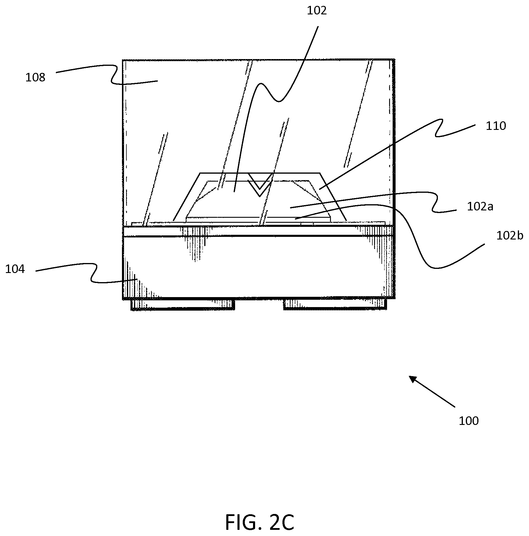
FIGS. 2A-2C shows one embodiment of an emitter package 100 according to the present invention. The emitter package 100, as with all packages shown hereafter, can be designed to achieve a UL 8750 class 4 rating (and/or any other relevant or similar ratings) while minimizing any negative effect on device output. The package 100 can include standard LED package components such as an emitter 102, a submount 104, one or more conductive traces 106, and a lens 108. In this case, the emitter 102 is direct-attached and/or flip-chip mounted on two conductive traces 106a,106b, although other embodiments are possible. A wavelength conversion material can be included in many different manners, with some examples being a conversion material on the emitter 102 with or without a binder, distributed in the lens, and/or as will be described below with regard to FIGS. 7A and 7B, for example.
The emitter 102 can include a substrate 102a, which in this case can form the primary emission surface. The diode region 102b of the emitter 102 (e.g. n-type, p-type, and light-emitting layers) and any other epitaxial and/or contact layers to the semiconductor layers can be between the substrate 102a and the traces 106a,106b.
Commonly assigned U.S. patent application Ser. No. 13/758,565 to Donofrio et al. and entitled "Light Emitting Diodes Including Light Emitting Surface Barrier Layers, and Methods of Fabricating Same", which is fully incorporated by reference herein in its entirety, describes the use of a layer of SiN directly on a light emitter on the system level including a sealed environment. This SiN layer can be used as a "carbon blocking layer" in sealed environments where outside gases such as oxygen cannot penetrate the system. This layer can prevent discoloration and/or charring which can cause both aesthetic and optical difficulties.
In some embodiments, the present invention is directed to the use of insulating materials as electrical insulators in an instance where a lens or encapsulant, which can provide a non-sealed and/or permeable environment, are removed or removable. These and other embodiments can be directed toward the component level as opposed to the system level. The component can then be used in any system. The insulating materials can include dielectrics such as SiN and/or SiO2, and/or can include nondielectrics. In some embodiments, the insulating layer(s) should have sufficient thickness to provide sufficient electrical isolation, as opposed to simply acting as a physical barrier. In some cases, the package 100 may not have sufficient lens adhesion to pass the adhesion portion of the class 4 test. For example, the package 100 may be relatively small, such as 1 mm.times.1 mm, 1.6 mm.times.1.6 mm, .ltoreq.2 mm by .ltoreq.2 mm, .ltoreq.5 mm.times..ltoreq.5 mm, and/or .ltoreq.10 mm.times.10 mm. Small packages typically have less lens adhesion. Some examples or small LED packages are the XLamp XQ-B and XLamp XQ-D from CREE, INC., the data sheets of which are fully incorporated by reference herein in their entirety. Many different small packages are possible.
The package 100 can instead be designed to pass the class 4 hi-pot test. If an insulating substrate such as sapphire is used, then the emitter portion of the component can pass the UL 8750 class 4 test without further components or processing. However, many modern substrate materials, including but not limited to materials not necessarily designed or used for their conductive properties, are at least somewhat conductive. For example, SiC substrates offer numerous advantages over insulating substrates such as sapphire, such as a better lattice match with semiconductor layers grown thereon, but will often fail the class 4 hi-pot test.
The package 100 can include an insulating layer 110. It is understood that all similarly positioned insulating layers described hereafter can have the properties described with regard to the insulating layer 110. The insulating layer 110 can be on and/or directly on some or all of the exposed surface of the emitter 102, including some or all of the exposed surface of the substrate 102a. The insulating layer 110 can be a coating or film, for example. The insulating layer 110 can be made of a material that is substantially transparent to the wavelength(s) of light emitted by the emitter 102. In one embodiment, the insulating layer 110 is a dielectric material or combination of dielectrics such as SiO.sub.2 and/or SiN, although many different dielectrics are possible. In another embodiment the insulating layer 110 is TiO.sub.2. In yet another embodiment the insulating layer 110 is a parylene polymer. In yet another embodiment the insulating layer 110 includes silicone and/or phosphor. Many different materials are possible. Combinations of the above, including but not limited to combinations of multiple layers having different contents, are possible, such as the combination of one or more dielectric sublayers and a phosphor/binder (e.g., phosphor/silicone) sublayer.
The insulating layer 110 can have a variety of thicknesses depending on its insulative properties. Typically, the lower the thickness, the less light will be absorbed by the insulating layer. In one embodiment, the thickness of the insulating layer 110 is greater than about 5000 A and/or between about 5000 A and about 5 .mu.m. In other embodiments, the thickness is about 1 .mu.m or greater, about 2 .mu.m or greater, about 5 .mu.m or less, about 1 .mu.m to about 3 .mu.m, and/or about 2 .mu.m. In one such embodiment, the insulating layer 110 includes about 1 .mu.m of dielectric material (e.g., SiO.sub.2 and/or SiN) and a phosphor/silicone layer. Exemplary phosphor/silicone layer thicknesses are between 60 .mu.m and 150 .mu.m, or about 100 .mu.m, although many different thicknesses are possible. In another embodiment, the insulating layer 110 includes about 2 .mu.m or more of a dielectric material (e.g., SiO.sub.2 and/or SiN). In another embodiment, the insulating layer 110 includes about 3 .mu.m or more, about 4 .mu.m or more, or about 4 .mu.m to about 5 .mu.m of parylene. If properly designed, these layer thicknesses can result in 1 .mu.men per watt losses of 5% or less, 3% or less, and/or about 1% or less compared to a similar package without such a layer. In some instances, an antireflective coating can be used which can result in 0% loss or enhanced extraction.
The above examples have also been shown to be able to withstand a typical class 4 hi-pot probe force of 1 lbf. The brittleness of the insulating layer 110 can be minimized by controlling temperature, pressure, and deposition rates, for example, resulting in a physically strong layer. As previously mentioned, the emitter-side interface of the insulating layer 110 and other insulating layers described herein can have better adhesion than the lens-side interface. The insulating layer 110 can be retained when one or more elements above it--such as the encapsulant or lens 108--are removed, thus preventing a potential shock and/or fire hazard.
The insulating layer 110 and other insulating layers described herein can include additives of many different kinds, such as, for example, wavelength converting particles and/or scattering particles as are known in the art.
In the embodiment shown in FIGS. 2A-2C, the insulating layer 110 can be conformal to the substrate 102a, as best seen in FIG. 2C. The thickness of the insulating layer 110 over the substrate 102a can be approximately uniform, defined herein as .+-.10% of the design or average thickness. In a conformal coating, the top surface of the coating layer (e.g. the insulating layer 110) can substantially follow the contours of the coated element (e.g. the emitter 102 and/or substrate 102a). Use of a conformal and/or uniform coating can result in a more uniform output from the emitter 102. In one example of a package according to the present invention, a conformal coating can be applied to a DA1000 LED chip from CREE, INC., the data sheet of which is fully incorporated herein by reference in its entirety. Many other types of chips can be used, including but not limited to the DA700, DA2432, and DA3547 chips from CREE, INC., the data sheet of each of which is fully incorporated by reference herein. The DA1000 includes a SiC substrate with a series of angled or beveled surfaces as its primary emission surface. A conformal coating according to one embodiment of the present invention can remain approximately at the same thickness within these subtractive areas as outside them, as shown in FIG. 2C.
As previously described, embodiments of the present invention can be designed such that all electrically active surfaces are insulated. While the embodiment of FIGS. 2A-2C shows traces that extend outside the footprint of the emitters, any of the embodiments herein described can include traces which are insulated in one or more of a number of different manners. For example and as will be described below, the traces can be covered with an insulating material, such as a solder mask for example. In other embodiments, a package can include one or more traces which are completely under one or more emitters and thus are not exposed on the submount's surface. Many different insulating devices, arrangements, and methods are possible, some of which will be described in detail below.
In other embodiments, the insulating layer 110 can be formed so as to have one or more planar surfaces, such as a planar top surface (note that if the top surface of the emitter is also planar, then such a coating would also be conformal). For example, FIGS. 3A-3C show a package 150 according to the present invention that can include an emitter 152 with a nonplanar top surface 152b. The package 150 can include an insulating layer 160 similar to or the same as the insulating layer 110. However, the insulating layer 160 can form a planar or substantially planar top surface 160b over the surface 152b. Some such embodiments can have reduced manufacturing complexity and costs.
Insulating layers such as those described above can be used in many different embodiments of the present invention, including all of those described hereafter. FIGS. 4A-4C show another embodiment of a package 200 according to the present invention which can include an insulating layer 210 similar to the insulating layer 110 from FIGS. 2A-2C. The package 200 can also include an emitter 202, a submount 204, traces, and a lens/encapsulant 208. Additionally, the package 200 can include a second insulating layer 212. The second insulating layer 212 can be reflective, and as such will be referred to herein as a reflective insulating layer 212, although this description should not be construed as limiting. The reflective insulating layer 212 and similar layers can come in the form of a solder mask and/or can cover some or all of the area outside of the footprint of the emitter, sometimes prior to the mounting of the emitter(s). Such methods will be discussed in detail below.
While the insulating layer 210 can serve to insulate the surfaces of the emitter 202 and substrate 202a should the lens 208 be removed, in order to meet UL 8750 class 4 standards the other exposed surfaces of the package must also not be electrically active. The reflective insulating layer 212 can serve to insulate these other surfaces and/or can serve to enhance light extraction. In the embodiment shown, the reflective insulating layer 212 can cover substantially all the top surface 204a of the submount 204 outside the footprint of the emitter 202. This can include the surfaces of the electrically active traces. In another embodiment, the surfaces of the traces are covered and less than the entirety of the top submount surface 204a is covered; in one such embodiment, the reflective insulating layer 212 covers substantially just the traces. In some embodiments, the top surface 204a can be reflective.
As discussed above, the reflective insulating layer 212 can be reflective. In one embodiment, the layer 212 comprises a diffuse reflective material and/or a white material, such as a white paint or coating. Some exemplary materials are available from WhiteOptics, LLC, of New Castle, Del. One exemplary product is the White96 Advanced Coating, which is designed to be 96% or more reflective, although many different products are possible. In another embodiment the layer can be specular.
Many different thicknesses are possible for the reflective insulating layer 212. In one embodiment, the layer 212 is about 25 .mu.m to about 75 .mu.m. In another embodiment, the layer 212 is about 50 .mu.m thick. Many other thicknesses are possible.
The use of a reflective material for the reflective insulating layer 212 can result in enhanced emission. For example, light that is internally reflected at the lens/ambient surface back into the lens may encounter the top surface 204a of the submount 204. By including a reflective material, this light can be reflected back toward the ambient and have another chance at emission. In other embodiments, a wavelength conversion material can be included on the surface 204a, whether by itself or in addition to the reflective material. This will be discussed in detail below with regard to FIGS. 7A and 7B. The above concepts can be referred to as "photon recycling," which is discussed in detail in commonly assigned U.S. patent application Ser. No. 13/770,389 to Lowes et al. and entitled "LED Package with Multiple Element Light Source and Encapsulant having Planar Surfaces," which is fully incorporated by reference herein in its entirety.
The thickness of the reflective insulating layer 212 can depend on many different factors including its insulative properties. In some embodiments, the layer is approximately 10 .mu.m to approximately 500 .mu.m, or about 150 .mu.m, although many different thicknesses are possible.
FIGS. 5A and 5B show a package 250 according to another embodiment of the present invention. The package 250 can include an emitter 252, submount 254, traces 256a,256b, and lens 258. The package 250 may not include a distinct reflective insulating layer such as the layer 212 from FIGS. 4A and 4B. Instead, an insulating layer 260 similar to or the same as the insulating layer 110 from FIGS. 2A-2C can cover both the exposed surfaces of the emitter 252 and any other electrically active surfaces, such as the surfaces of the traces 256. In the embodiment shown, the insulating layer 260 covers substantially all the top surface 254a of the submount 254 including the traces 256, although in other embodiments it covers less than all the top surface 254a.
The package 250 can still have an emission that is enhanced due to the reflection of internally reflected light. For example, the traces 256a,256b and/or the top surface 254a of the submount 254 can be reflective. For example, the traces 256a,256b can be reflective metal. Because the insulating layer 260 can be substantially transparent to the wavelengths of light being emitted by the package 250, light can pass through the insulating layer 260 and be reflected by the traces 256a,256b and/or the top surface 254. In some embodiments, the traces 256a,256b can cover 50% or more of the top surface 254a of the submount 250 outside the footprint of the emitter 252. In other embodiments, the traces 256a,256b can cover 80% or more of this surface, and in other embodiments can cover 90% or more of this surface.
FIGS. 6A and 6B show a package 300 according to another embodiment of the present invention. The package 300 can include an emitter 302, submount 304, traces 306a,306b, lens 308, and an insulating layer 310 similar to or the same as the insulating layer 260 from FIGS. 5A and 5B. Although the package 300 is shown without a reflective insulating layer, it is understood that a layer similar to the reflective insulating layer 212 from FIGS. 4A-4C could be included, such as in an embodiment where the insulating layer 310 covers only the exposed surfaces of the emitter 302. The package 300 is similar in many respects to the package 250 from FIGS. 5A and 5B, with an insulating layer 310 covering substantially all of the top surface of the submount 304, although many different embodiments are possible. The primary difference between the packages 300 and 250 is that the substrate of the emitter 302 has been thinned, such as a substrate of 100 .mu.m or less. For comparison, a typical DA 1000 emitter from CREE, INC. can have a substrate of 300 .mu.m to 400 .mu.m, or about 335 .mu.m. The thinning of the substrate can result in enhanced emission as less light will be absorbed by the substrate before passing into the insulating layer 310. Substrate removal and thinning is described, for example, in commonly assigned U.S. Pat. No. 7,932,111 to Edmond and entitled "Substrate Removal Process for High Light Extraction LEDs", which is fully incorporated by reference herein in its entirety. Other substrate removal processes, such as grinding and etching, are known in the art. In some embodiments of the present invention, such as those with vertically oriented emitters as will be described with regard to FIGS. 13A and 13B, the substrate could be completely removed to enhance light extraction even further.
In embodiments of the present invention with emitters not having a substrate or having a reduced substrate, such as the emitter 302, the materials and thickness of the insulating layer can sometimes be the same as described above with regard to the insulating layer 110 from FIGS. 2A-2C. However, in some cases the thickness of the insulating layer may be greater, such as due to the fact that the substrate does not provide any insulation (i.e., the presence of a semi-insulating/semi-conductive substrate in some embodiments may provide at least some insulation and therefore allow for the use of a thinner insulating layer than would otherwise be needed). Insulating layers over a substrateless emitter or an emitter with a thinned substrate, such as the insulating layer 310, can in some embodiments be about 2 .mu.m or greater, in some embodiments about 2 .mu.m to about 3 .mu.m, and/or in some embodiments about 3 .mu.m or greater.
FIGS. 7A and 7B show a package 350 according to another embodiment of the present invention. The package 350 can include an emitter 352, submount 354, traces, and lens 358. The embodiment shown is similar in many respects to the package 200 from FIGS. 4A-4C in that it can include an insulating layer 360 and a reflective insulating layer 362; however, it is understood that the package 350 can include any of the insulating layer arrangements described above with regards to FIGS. 2A-6B or described hereafter. The package 350 can include a wavelength conversion layer 364 that can include wavelength conversion elements such as phosphor, for example. The layer 364 can also comprise a binder, and different materials can be used for the binder, with materials preferably being robust after curing and substantially transparent in the visible wavelength spectrum. Suitable materials include silicones, epoxies, glass, inorganic glass, dielectrics, BCB, polymides, polymers and hybrids thereof. In embodiments where the wavelength conversion layer 364 includes an insulating material such as a dielectric, the insulating layer 360 may not be needed as the wavelength conversion layer 364 can sufficiently insulate the emitter 352. A preferred material is silicone because of its high transparency and reliability in high power LEDs. Suitable phenyl- and methyl-based silicones are commercially available from Dow.RTM. Chemical. The binder can be cured using many different curing methods depending on different factors such as the type of binder used. Different curing methods include but are not limited to heat, ultraviolet (UV), infrared (IR) or air curing. Further, it should be understood that phosphor particles can be applied without a binder.
Although other embodiments are possible, in the embodiment shown the wavelength conversion layer 364 covers substantially all of the top surface of the submount 354, including the surfaces of the emitter 352. This can result in photon recycling conversion previously described and described in U.S. patent application Ser. No. 13/770,389 to Lowes et al. In another embodiment, the wavelength conversion layer 364 does not cover the entire top surface, but does cover the emitter 352. In the specific embodiment shown, the wavelength conversion layer 364 is deposited on the insulating layer 360 and reflective insulating layer 362, although other embodiments are possible. This order, however, can be advantageous, in that deposition before the reflective layer could prevent conversion of recycled light, and deposition before the insulating layer could cause portions of the wavelength conversion layer to be displaced during deposition of the insulating layer. However, in another embodiment the insulating layer can be between the reflective layer and the wavelength conversion layer.
It should be understood that the exact configuration shown in FIGS. 7A and 7B is only one embodiment and should not be construed as limiting. Wavelength conversion layers such as the layer 364 and those described above can be utilized in any embodiments of the present invention, including but not limited to those described herein, as would be understood by one of skill in the art. Further, it is understood that wavelength conversion layers according to the present invention can be applied before or after any of the insulating layers described herein.
Although all of the previous embodiments have shown only a single emitter, any of these embodiments and those described below can include two or more emitters. For example, FIGS. 8A and 8B show a package 400 similar in many ways to the package 100 from FIGS. 2A-2C, but with two emitters 402a,402b. The package 400 can include a submount 404 and lens 408, as well as traces 406 that can be patterned to accommodate the number of emitters present. The package 400 can include insulating layers 410a,410b which cover the emitters 402a,402b. The remainder of the top surface of the submount 404 is shown as uncovered, but it is understood that any of the layers described above can be included, such as a reflective insulating layer and/or a wavelength conversion layer, for example, or the insulating layers 410a,410b could expand further beyond the footprint of the emitters 402a,402b.
FIGS. 9A and 9B shows another multi-emitter package according to the present invention. The package 450 can include two or more emitters, such as the five emitters 452 shown, and can also include a submount 454 with top surface 454a, conductive traces (not shown), and a lens 458. In embodiments where a large portion of the top surface of the submount is covered by emitters, such as the top surface 454a with a large portion covered by emitters 452, the manufacturing efficiency benefits of covering the entire submount top surface with an insulating layer may outweigh the additional material expenditure. For example, the package 450 includes a top surface 454a which is covered by an insulating layer 460 (which can be similar to or the same as any of the above insulating layers). It is understood that different types of other elements not explicitly shown in the package 450 can also be included (e.g., a reflective insulating layer, a wavelength conversion layer, etc.).
Additionally, FIGS. 9A and 9B show two emitters 452a,452b having undercuts. The emitters 452a,452b include at least one outer and/or side surface which angles inward as it approaches the submount 454. The coating of the insulating layer on undercut emitters can be done in many different manners, two of which are best shown in FIG. 9B. The emitter 452a, for example, is coated conformally, where the thickness of the insulating layer 460 is substantially uniform around the entire emitter 452a. This can result in a more uniform emission. The emitter 452b, on the other hand, is coated in a "box" manner which can result in the insulating layer 460 having substantially vertical sidewalls which do not follow the contour of the undercut. In a similar embodiment, the insulating layer over an emitter can form a parabolic shape and/or have sidewalls angling away from the emitter as they approach the submount. These methods can result in reduced manufacturing complexity. It is understood that any of the packages described herein, including those described above and hereafter, can include one or more emitters having undercuts which can be coated in any number of ways, including but not limited to conformal, box, and parabolic coatings.
FIG. 10A shows an emitter according to the present invention. The emitter 500 bears some similarities to emitters described in commonly assigned U.S. patent application Ser. No. 13/759,229 to Hussell et al. and entitled "Submount-Free Light Emitting Diode (LED) Components and Methods of Fabricating Same", and commonly assigned U.S. patent application Ser. No. 14/053,404 to Heikman et al. and entitled "Chip with Integrated Phosphor", each of which is fully incorporated by reference herein in its entirety. U.S. patent application Ser. No. 14/053,404 to Heikman et al. refers to the formation of "virtual wafers," or individual devices bound together via one or more layers instead of a submount wafer. Layers holding together the devices of a virtual wafer can include, for example, phosphor layers, silicone layers, and/or glass layers. FIG. 10A shows a single device 500, but other devices could be, for example, on the left and right of the device 500 and connected via single layers or combinations of layer 510 and/or layer 514 and/or layer 516, which will be described below.
The emitter 500 can include a substrate 504 and a diode region (not shown, on the bottom surface of the substrate 504), as well as contacts 506 which can be mounted on traces in a package. In the embodiment shown the emitter 500 also includes an optional reflective layer 507. In the embodiment shown, the emitter includes a phosphor layer 514 and a utility layer 516 which can be made of many different materials, including but not limited to silicone and glass. Utility layers according to the present invention can act as lenses and/or encapsulants. While the utility layer 516 is shown on both the top and side surfaces in this embodiment, it can be on less than all of these surfaces, such as only on the top surface. Other embodiments are possible. Utility layers are discussed in detail in U.S. patent application Ser. No. 14/053,404 to Heikman et al.
In addition, the emitter 500 can include an insulating layer 510, which can be deposited before or after the emitter 500 is mounted on a submount. The insulating layer can be below the utility layer 516 such that if the utility layer 516 is sheared off, the surface of the emitter 504 is still insulated. The insulating layer 510 can be similar to or the same as the insulating layers previously described, such as the layer 110 from FIGS. 2A-2C.
It is understood that embodiments of the present invention can include many different layers, including but not limited to the layers 510,514,516 shown in FIG. 10A, in many different orders. FIGS. 10B-10D show examples of some variations, but many different variations are possible as would be recognized by one of skill in the art.
FIG. 10B shows an emitter 520 that can include many of the same elements as the emitter 500, with the same elements shown with the same indicators. However, the emitter 520 includes an insulating layer 521 that is conformal to the substrate 504 and diode layers. The emitter 520 can then optionally include a utility layer 526, which can be transparent and which can, by itself or in combination with one or more other layers, hold together multiple emitters 520 in a virtual wafer. In emitters not already including a wavelength converter, such as the emitter 520 and the emitter 540 from FIG. 10D, wavelength conversion material can be provided in another manner such as that described above with regard to phosphor layers or other manners known in the art (e.g., placement in a lens, etc.).
FIG. 10C shows an emitter 530. The emitter 530 can include a phosphor layer 534. However, instead of the traditional silicone or glass utility layer, the emitter 530 can include an insulating layer 531 comprising, for example, a dielectric. The insulating layer 531 can serve both as an insulator for purposes of meeting class 4 rating standards and/or can serve as a utility layer for virtual wafer purposes.
FIG. 10D shows an emitter 540 that is similar in many respects to the emitter 530. However, the emitter 540 may not include a phosphor layer, but instead may only include an insulating layer 541. Similar to the insulating layer 531, the insulating layer 541 can serve as an insulator for class 4 rating standards and/or can serve as a utility layer for virtual wafer purposes.
FIGS. 11A and 11B show a package according to the present invention that includes the emitter 502 from FIG. 10B, although it is understood that any one or more of the emitters described above with regard to FIGS. 10A-10D and/or U.S. patent application Ser. No. 14/053,404 can be included in packages in the present invention. Further, any of the other components described above, although not depicted, could be included. For example, because the emitter 520 did not necessarily include a wavelength conversion material, a wavelength conversion layer similar to the layer 364 from FIGS. 7A and 7B could be included.
As previously discussed, while one failure point in the UL8750 hi-pot test is conduction occurring through an exposed surface, another failure method is arcing. Further, arcing can cause damage to an emitter. Underfill can be used both to increase the voltage at which arcing occurs and to control the location where it occurs. Underfill and its uses are described in commonly assigned applications U.S. patent application Ser. No. 13/369,996 to Donofrio and entitled "Gel Underfill Layers for Light Emitting Diodes and Methods of Fabricating Same", and U.S. patent application Ser. No. 12/008,477 to Chitnis et al. and entitled "Flip-Chip Phosphor Coating Method and Devices Fabricated Utilizing Method", each of which is fully incorporated by reference herein in its entirety. One common underfill material is silicone, and in particular a gel-like silicone can be used.
As can be seen in, for example, FIGS. 2A-2C and FIGS. 10A-10D, a small gap can sometimes remain between traces on a submount and/or contacts on the bottom of an emitter. FIGS. 12A and 12B show a package 600 similar in many respects to the package 100 from FIGS. 2A-2C and including such gaps. Underfill 618 can be deposited before or after an insulating layer in order to fill these gaps, which can lessen the likelihood of arcing and/or of an electrical short, and can also contribute to emitter stability.
Underfill can also be used to move the critical point for arcing further away from the emitter 602 and therefore lessen the chance of arcing damage occurring. In the UL 8750 hi-pot test of the package 100 from FIGS. 2A-2C, the critical point for arcing will likely be the point at the edge or corner of the insulating layer. By including underfill at this boundary in a manner similar to the underfill 618 in FIGS. 6A and 6B, the critical point for arcing can be moved to the outside edge of the underfill further from the emitter 602. Should arcing occur, the likelihood of damage to the emitter 602 can thus be lessened. It should be noted that while underfill 618 is not used with any layers other than an insulating layer 610 in the embodiment shown, it can be used with any of the layers described above, including but not limited to a reflective insulating layer and/or a wavelength conversion layer.
Another advantage of the use of underfill is to cover small exposed conductive areas that may still be present due to manufacturing realities. For example, where an insulating layer such as a solder mask is placed prior to placement of an emitter, the solder mask opening may be slightly larger than the emitter. Small areas of conductive trace, such as areas with dimensions of about 10 .mu.m to about 150 .mu.m, may be exposed. An underfill can cover these areas, which may otherwise be accessible to hi-pot probing. Another such instance is when one or more face-down contacts are not completely buried by the emitters. These are just a few instances where underfill can have advantages, and many other embodiments are possible.
The above embodiments of packages have focused upon horizontally-oriented packages that are direct-attached and/or flip-chip mounted on a submount, which have distinct advantages in that the contacts are "buried" and not exposed. However, other embodiments are possible, including both vertically oriented devices and horizontally oriented devices with contacts on a top surface. FIGS. 13A and 13B show one such package 650 according to an embodiment of the present invention which can include an emitter 652, a submount 654, traces 656a,656b, and a lens 658. An exemplary emitter is the XT290 from CREE, INC., the data sheet of which is fully incorporated by reference herein in its entirety, although many different types of emitters are possible. Typically packages having wire bonds that do not meet the class 4 lens adhesion standards cannot achieve a class 4 rating, as the wire bonds will be exposed if the lens were to be removed. However, the package 650 can include an insulating layer 660 that can be designed to envelope the wire 657, which can connect the trace 656a to the emitter 652, such as to a topside contact on the emitter 652. The insulating layer can also cover all of the trace 656a. The package 650 could also include, for example, a reflective insulating layer, a wavelength conversion layer, or any of the other elements discussed above with regard to other embodiments. In order to cover the necessary surfaces, an insulating layer such as that described above may be thicker than those previously described.
Other embodiments with some of the attributes of that shown in FIGS. 13A and 13B are also possible. For example, FIG. 13C shows a package 670 according to one embodiment of the present invention. The package 670 includes a rectangular vertically-oriented emitter 672, which can include topside and bottomside contacts. Some examples of such emitters include the EZ line of emitters available from CREE, INC., although many different emitters are possible. The emitter 672 can be on, such as mounted on, a conductive trace or contact 676b. A topside contact can be connected via a medium such as a wire bond to a conductive trace or contact 676a, which can be on the top surface of the submount 674, for example. The emitter 672, contacts/traces 676a,676b, and/or conductive medium 677 can be covered by the insulating layer 671, which can have any of the properties described above with regard to insulating layers according to the present invention. By covering all conductive surfaces beneath the encapsulant, the package 670 can meet the UL 8750 class 4 rating standards.
FIG. 13D shows a package 680 with many similarities to the package 670 from FIG. 13C. The package 680, however, can include a horizontally-oriented emitter 682. The emitter 682 can include two top-side contacts (not shown), which can be electrically connected via conductive medium such as wires 687a,687b. The wires 687a,687b can be connected to conductive traces or contacts 686a,686b, which can be on the top surface of the submount 684. In the embodiment shown, all conducting surfaces, including the contacts 686a,686b, conductive media 687a,687b, and/or the emitter 682 can be covered by an insulating layer 681, which can have any of the properties described above with regard to insulating layers according to the present invention.
Any of the layers described above with regard to FIGS. 2A-13B can be applied in a number of different ways, including but not limited to chemical vapor deposition (CVD), physical vapor deposition (EVD), spinning on, dispensing, brushing, painting, dipping, spraying, and/or screen-printing, for example. One preferred method for depositing insulating layers according to the present invention is CVD.
FIGS. 14A-14D show different fabrication methods according to embodiments of the present invention, with optional steps shown with dashed arrow lines (although other steps may also be omitted in some embodiments). In the embodiment of FIG. 14A, after providing a submount with traces such as the traces 106a,106b from FIGS. 2A-2C, a reflective insulating layer such as the layer 212 from FIGS. 4A-4C can optionally be deposited. This layer can cover areas outside the area in which one or more emitters are to be mounted. Example areas include the entire submount top surface outside the emitters, any exposed conductive surfaces, and/or exposed surfaces of the traces (if the traces are exposed and/or outside the footprint of the emitter(s)). In step 1406, one or more emitters can be mounted on areas at least partially, and sometimes wholly, uncovered by the reflective insulating layer (if present). The insulating layer can then be applied to the emitter(s), as previously described. In an optional step, a converter can be applied in one of many different manners. For example, a wavelength conversion layer similar to layer 364 from FIGS. 7A-7C can be deposited over most or all of the top surface of the submount. Alternatively, a coating of wavelength conversion material can be applied selectively to areas on and/or around the emitter(s). In another method, this step is skipped altogether and/or a conversion material may be included in the lens, which is attached in step 1412. The lens can be attached by, for example, molding.
Many different variants of the method shown in FIG. 14A are possible. For example, as shown in FIG. 14B, a reflective insulating layer could be applied after one or more emitters are already attached. As another example shown in FIG. 14C, one to three or even more than three different steps can be completed in any order between the mounting of the emitter(s) and the attachment of a lens, with the three steps shown including applying a converter, applying an insulating layer to emitter(s), and applying a reflective insulating layer in areas outside the emitter footprint, although many steps are possible.
FIG. 14D shows a method specifically adapted for fabricating emitters according to the present invention that require a wire bond. It is understood that steps described above could also be included in the method of FIG. 14D at various points in the process. In this method, after an emitter is mounted on one trace, the emitter is electrically connected to another trace. Then, an insulating layer (e.g., the insulating layer 660 from FIGS. 13A and 13B) can be applied and cover all exposed electrical surfaces, including exposed conductive surfaces of the emitter, trace(s), and connecting medium or component (e.g., a wire). One method in particular of completing this step is to mold and cure the insulating layer such that it covers these conductive materials, although many different formation/deposition methods are possible.
In any of the above methods, the use of a descumming process may also increase the effectiveness of the insulation layer which lies between the probes and conductive surfaces of the device(s) during a hi-pot test of the devices. For example, if a photo resist is used during any processes involved in generating the insulating layer, a descumming process could remove any remaining residue so as to reduce the likelihood of defects in the electrical insulation, such as pinholes, variable thickness, and/or poor adhesion.
Examples and Test Results
A control first round of testing was conducted on a package including a DA1000 LED chip from CREE, INC. The DA1000 includes a silicon carbide substrate. All packages failed the hi-pot test via conduction through the substrate in less than 20 seconds at a voltage of about 200 VAC, well under the 500 VAC class 4 requirement.
A second round of testing was conducted on a package including a DA3547 LED chip from CREE, INC., also including a silicon carbide substrate. The substrates were covered with one or more dielectric layers. The test was run with a DC source three times on each component with a typical metal probe, and three times with a metal probe and a Cu cushion in an attempt to lessen the likelihood of mechanical failure, such as due to brittleness of the dielectric layers used in the tests. The following components passed both with and without the Cu cushion:
1. De-scum, 5000 A SiO.sub.2, 5000 A SiN, phosphor/silicone layer
2. De-scum, 5000 A SiN, 5000 A SiO.sub.2, phosphor/silicone layer
3.5000 A SiO.sub.2, 5000 A SiN, phosphor/silicone layer
4. 5000 A SiN, 5000 A SiO.sub.2, phosphor/silicone layer
5. 2 .mu.m SiN (passed hi-pot threshold criteria, electrical breakdown at 800-830 VDC via arcing)
6. 4 .mu.m-5 .mu.m parylene, phosphor/silicone layer
It is understood that different emitter package embodiments can have different combinations of the emitters, layers, and/or other components described above. Each of the configurations of insulating layers, reflective insulating layers, and wavelength conversion mechanisms such as wavelength conversion layers can be used in any combination and be deposited in any order. It is understood that the different emitters described above are only a few of the many different emitters that can be used in packages according to the present invention.
The packages according to the present invention can serve as the light source for lamps such as those described in U.S. patent application Ser. No. 13/034,501, to Le et al., entitled "Solid State Lamp", and U.S. patent application Ser. No. 13/028,946, to Le et al., entitled "High Efficacy LED Lamp With Remote Phosphor and Diffuser Configuration", each of which is fully incorporated herein by reference in its entirety.
The LED packages can also be used in troffer type lamp fixtures such as those described in U.S. patent application Ser. No. 13/368,217 to Pickard et al., entitled "Multiple Panel Troffer Style Light Fixture", and U.S. patent application Ser. No. 12/873,303, Edmond et al., entitled "Troffer-Style Fixture", each of which is fully incorporated by reference herein in its entirety.
The LED packages can also be used in many other lighting applications such as LED displays, LED street lighting, residential LED downlighting, etc. Some LED package embodiments of the present invention are particularly applicable to fluorescent tube replacement LED lighting with the emission pattern of the LED packages being desirable for linear arrays such as those used in fluorescent tube replacements.
The LED packages can be arranged with many different features beyond those described above. Some embodiments can comprise electrostatic discharge (ESD) protection elements or devices. Others of the LED packages can be arranged with secondary optics to further disperse, spread or columnate the package beam profile. In still other embodiments, different ones of the LEDs within the package can be mounted higher than others of the LEDs to provide the desired LED package emission pattern.
Although the embodiments above are often described herein with reference to LED packages with conversion material layers, it is understood that other embodiments can be provided without a conversion material layer. Some of these embodiments can comprise a blue, red or green LED chip by itself to provide LED packages emitting blue, red or green light. Other embodiments can also comprise multiple LED chips emitting different colors of light such as red, green or blue emitting LEDs, or red, green, blue, and white emitting LEDs, or red, green, blue, and amber LEDs. These are only some of the combinations that are possible in different embodiments according to the present invention.
The LED packages can be arranged with many additional features, such as adaptors or connectors to allow for handing and mounting of these relatively small packages. The different LED package embodiments can comprise different markings or other features to assist in alignment, or the mounting area can have marks or features to assist in alignment and mounting of the LED packages. Some such features are described in U.S. patent application Ser. No. 14/271,116 to Wilcox et al. and entitled "Optical Element with Integrated Indicator," which is fully incorporated by reference herein in its entirety.
Although the present invention has been described in detail with reference to certain preferred configurations thereof, other versions are possible. The invention can be used in any light fixtures where a uniform light or a near uniform light source is required. In other embodiments, the light intensity distribution of the LED module can be tailored to the particular fixture to produce the desired fixture emission pattern. Therefore, the spirit and scope of the invention should not be limited to the versions described above.
* * * * *
References
D00000
D00001
D00002
D00003
D00004
D00005
D00006
D00007
D00008
D00009
D00010
D00011
D00012

D00013

D00014

D00015

D00016

D00017

D00018

D00019

D00020

D00021

D00022
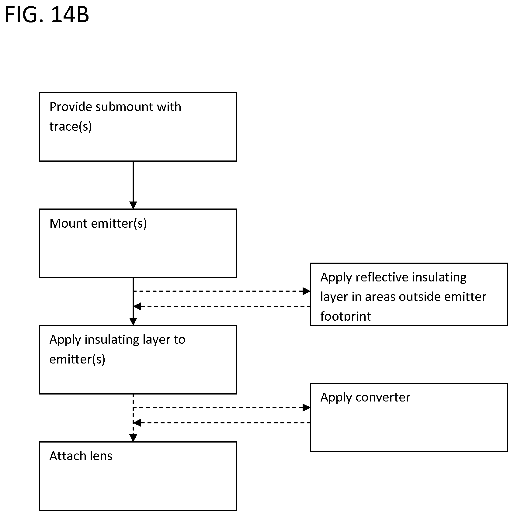
D00023
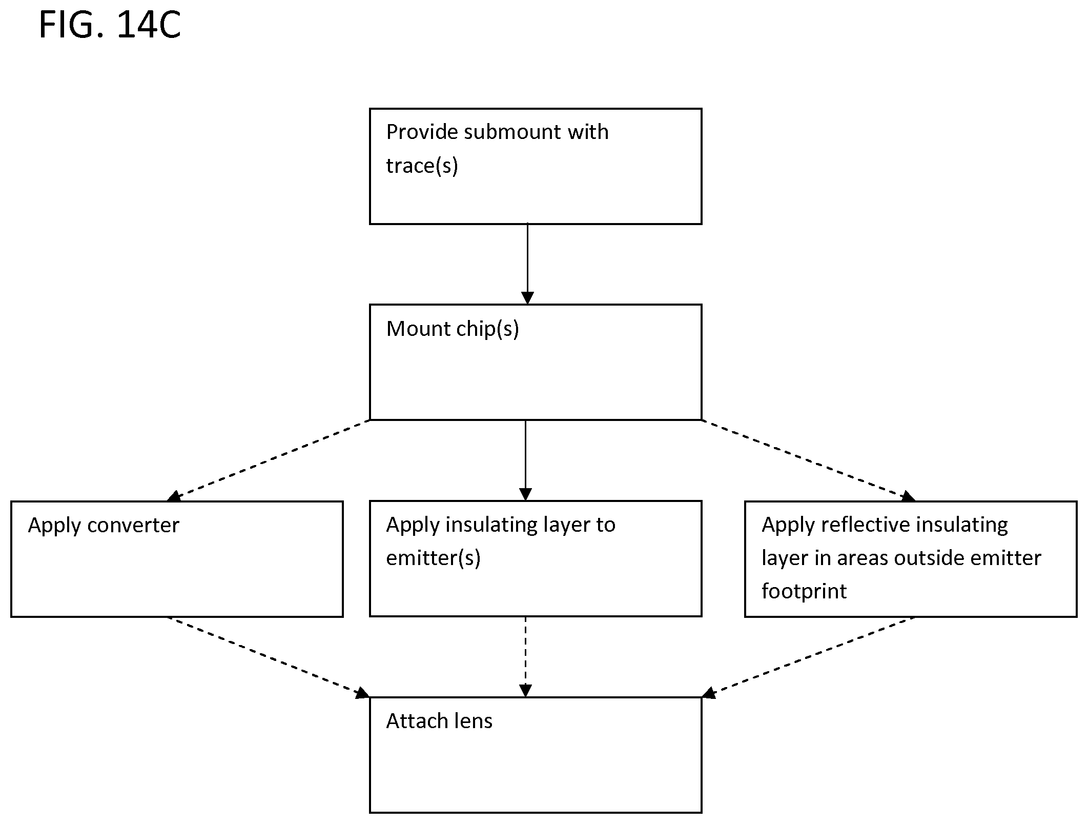
D00024

XML
uspto.report is an independent third-party trademark research tool that is not affiliated, endorsed, or sponsored by the United States Patent and Trademark Office (USPTO) or any other governmental organization. The information provided by uspto.report is based on publicly available data at the time of writing and is intended for informational purposes only.
While we strive to provide accurate and up-to-date information, we do not guarantee the accuracy, completeness, reliability, or suitability of the information displayed on this site. The use of this site is at your own risk. Any reliance you place on such information is therefore strictly at your own risk.
All official trademark data, including owner information, should be verified by visiting the official USPTO website at www.uspto.gov. This site is not intended to replace professional legal advice and should not be used as a substitute for consulting with a legal professional who is knowledgeable about trademark law.