Method and device concerning III-nitride edge emitting laser diode of high confinement factor with lattice matched cladding layer
Han , et al. Fe
U.S. patent number 10,554,017 [Application Number 15/574,739] was granted by the patent office on 2020-02-04 for method and device concerning iii-nitride edge emitting laser diode of high confinement factor with lattice matched cladding layer. This patent grant is currently assigned to Yale University. The grantee listed for this patent is Yale University. Invention is credited to Jung Han, Yufeng Li, Ge Yuan.


View All Diagrams
| United States Patent | 10,554,017 |
| Han , et al. | February 4, 2020 |
Method and device concerning III-nitride edge emitting laser diode of high confinement factor with lattice matched cladding layer
Abstract
Edge-emitting laser diodes having high confinement factors and lattice-matched, porous cladding layers are described. The laser diodes may be formed from layers of III-nitride material. A cladding layer may be electrochemically etched to form a porous cladding layer having a high refractive index contrast with an active junction of the device. A transparent conductive oxide layer may be deposited to form a top-side cladding layer with high refractive index contrast and low resistivity.
| Inventors: | Han; Jung (Woodbridge, CT), Li; Yufeng (Shaanxi, CN), Yuan; Ge (New Haven, CT) | ||||||||||
|---|---|---|---|---|---|---|---|---|---|---|---|
| Applicant: |
|
||||||||||
| Assignee: | Yale University (New Haven,
CT) |
||||||||||
| Family ID: | 57320858 | ||||||||||
| Appl. No.: | 15/574,739 | ||||||||||
| Filed: | May 19, 2016 | ||||||||||
| PCT Filed: | May 19, 2016 | ||||||||||
| PCT No.: | PCT/US2016/033270 | ||||||||||
| 371(c)(1),(2),(4) Date: | November 16, 2017 | ||||||||||
| PCT Pub. No.: | WO2016/187421 | ||||||||||
| PCT Pub. Date: | November 24, 2016 |
Prior Publication Data
| Document Identifier | Publication Date | |
|---|---|---|
| US 20180152003 A1 | May 31, 2018 | |
Related U.S. Patent Documents
| Application Number | Filing Date | Patent Number | Issue Date | ||
|---|---|---|---|---|---|
| 62163811 | May 19, 2015 | ||||
| Current U.S. Class: | 1/1 |
| Current CPC Class: | H01S 5/34333 (20130101); H01S 5/3213 (20130101); H01S 5/3219 (20130101); H01S 5/305 (20130101); H01S 5/3211 (20130101); H01S 5/2009 (20130101); H01S 5/2081 (20130101); H01S 5/0422 (20130101); H01S 5/3214 (20130101); H01L 21/306 (20130101); H01S 2304/04 (20130101) |
| Current International Class: | H01S 5/20 (20060101); H01S 5/32 (20060101); H01S 5/343 (20060101); H01L 21/306 (20060101); H01S 5/30 (20060101) |
References Cited [Referenced By]
U.S. Patent Documents
| 5262021 | November 1993 | Volker et al. |
| 5307361 | April 1994 | Kahen |
| 5502787 | March 1996 | Capasso |
| 5509026 | April 1996 | Sasaki et al. |
| 5644156 | July 1997 | Suzuki et al. |
| 5818861 | October 1998 | Tan et al. |
| 5919430 | July 1999 | Hasenzahl et al. |
| 6306672 | October 2001 | Kim |
| 6320206 | November 2001 | Coman et al. |
| 6537838 | March 2003 | Stockman |
| 6597017 | July 2003 | Seko et al. |
| 6597490 | July 2003 | Tayebati |
| 6759310 | July 2004 | Hiroshi |
| 6990132 | January 2006 | Kneissl et al. |
| 7271417 | September 2007 | Chen |
| 7750234 | July 2010 | Deng et al. |
| 7751455 | July 2010 | Kneissl |
| 7923275 | April 2011 | Nakagawa |
| 7989323 | August 2011 | Shenai-Khatkhate |
| 8343788 | January 2013 | Kuo et al. |
| 8344409 | January 2013 | Peng et al. |
| 8497171 | July 2013 | Wu et al. |
| 8507925 | August 2013 | Kuo et al. |
| 8519430 | August 2013 | Peng et al. |
| 9206524 | December 2015 | Zhang et al. |
| 9356187 | May 2016 | Ryu et al. |
| 9583353 | February 2017 | Han |
| 2002/0036295 | March 2002 | Nunoue et al. |
| 2002/0070125 | June 2002 | Ng et al. |
| 2002/0075929 | June 2002 | Cunningham |
| 2002/0153595 | October 2002 | Tayanaka |
| 2002/0158265 | October 2002 | Eisenbeiser |
| 2003/0178633 | September 2003 | Flynn et al. |
| 2003/0189963 | October 2003 | Deppe et al. |
| 2004/0021147 | February 2004 | Ishibashi et al. |
| 2004/0104398 | June 2004 | Hon et al. |
| 2005/0029224 | February 2005 | Aspar et al. |
| 2005/0184307 | August 2005 | Li et al. |
| 2005/0224816 | October 2005 | Kim et al. |
| 2005/0242365 | November 2005 | Yoo |
| 2006/0046513 | March 2006 | Shea et al. |
| 2006/0110926 | May 2006 | Hu et al. |
| 2006/0199353 | September 2006 | Kub et al. |
| 2007/0007241 | January 2007 | DeLouise |
| 2007/0040162 | February 2007 | Song |
| 2007/0085100 | April 2007 | Diana et al. |
| 2007/0111345 | May 2007 | Wong et al. |
| 2007/0194330 | August 2007 | Ibbetson et al. |
| 2007/0284607 | December 2007 | Epler et al. |
| 2008/0029773 | February 2008 | Jorgenson |
| 2008/0067532 | March 2008 | Watson et al. |
| 2008/0179605 | July 2008 | Takase et al. |
| 2008/0280140 | November 2008 | Ferrari et al. |
| 2008/0285610 | November 2008 | Hall et al. |
| 2008/0296173 | December 2008 | Mishra |
| 2008/0298419 | December 2008 | Hori et al. |
| 2009/0001416 | January 2009 | Chua et al. |
| 2009/0117675 | May 2009 | Yamanaka et al. |
| 2009/0140274 | June 2009 | Wierer, Jr. et al. |
| 2009/0143227 | June 2009 | Dubrow et al. |
| 2009/0168819 | July 2009 | Otoma |
| 2009/0173373 | July 2009 | Walukiewicz et al. |
| 2010/0195689 | August 2010 | Ariga et al. |
| 2010/0246625 | September 2010 | Kawashima |
| 2010/0270649 | October 2010 | Ishibashi et al. |
| 2010/0317132 | December 2010 | Rogers et al. |
| 2011/0076854 | March 2011 | Takeo et al. |
| 2011/0101391 | May 2011 | Mild et al. |
| 2011/0188528 | August 2011 | Kisin |
| 2012/0018753 | January 2012 | Hao et al. |
| 2012/0025231 | February 2012 | Krames et al. |
| 2012/0068214 | March 2012 | Kuo et al. |
| 2012/0189030 | July 2012 | Miyoshi |
| 2012/0205665 | August 2012 | Nam |
| 2013/0011656 | January 2013 | Zhang |
| 2013/0050686 | February 2013 | Wunderer et al. |
| 2013/0134457 | May 2013 | Peng et al. |
| 2013/0140517 | June 2013 | Tang et al. |
| 2013/0210180 | August 2013 | Wang |
| 2013/0248911 | September 2013 | Hwang et al. |
| 2013/0328102 | December 2013 | Peng et al. |
| 2013/0334555 | December 2013 | Hsieh et al. |
| 2014/0003458 | January 2014 | Han |
| 2014/0048830 | February 2014 | Kuo et al. |
| 2014/0064313 | March 2014 | Sato et al. |
| 2014/0191369 | July 2014 | Tsuchiya et al. |
| 2014/0339566 | November 2014 | Seo et al. |
| 2015/0303655 | October 2015 | Han et al. |
| 2016/0153113 | June 2016 | Zhang et al. |
| 2016/0197151 | July 2016 | Han et al. |
| 2017/0133826 | May 2017 | Han |
| 2017/0237234 | August 2017 | Han et al. |
| 101443887 | May 2009 | CN | |||
| 102782818 | Nov 2012 | CN | |||
| 103762286 | Apr 2014 | CN | |||
| H05-315316 | Nov 1993 | JP | |||
| H10-135500 | May 1998 | JP | |||
| H11-195562 | Jul 1999 | JP | |||
| 2000-349267 | Dec 2000 | JP | |||
| 2001-223165 | Aug 2001 | JP | |||
| 2004-055611 | Feb 2004 | JP | |||
| 2005-244089 | Sep 2005 | JP | |||
| 2007-073945 | Mar 2007 | JP | |||
| 2007-518075 | Jul 2007 | JP | |||
| 2007-335879 | Dec 2007 | JP | |||
| 2009-055056 | Mar 2009 | JP | |||
| 2009-067658 | Apr 2009 | JP | |||
| 2009-231833 | Oct 2009 | JP | |||
| 2009-239034 | Oct 2009 | JP | |||
| 2010-218510 | Sep 2010 | JP | |||
| 2000-0038997 | Jul 2000 | KR | |||
| 10-0480764 | Jun 2005 | KR | |||
| WO 2005/066612 | Jul 2005 | WO | |||
| WO 2009/048265 | Apr 2009 | WO | |||
| WO 2011/094391 | Aug 2011 | WO | |||
| WO 2013/050686 | Apr 2013 | WO | |||
Other References
|
International Search Report and Written Opinion for International Application No. PCT/US2013/046852, dated Oct. 29, 2013. cited by applicant . International Preliminary Report on Patentability for International Application No. PCT/US2013/046852, dated Jan. 8, 2015. cited by applicant . Extended European Search Report for European Application No. 11737629.3, dated Oct. 12, 2017. cited by applicant . International Search Report and Written Opinion for International Application No. PCT/US2011/022701, dated Apr. 8, 2011. cited by applicant . International Preliminary Report on Patentability, dated Aug. 9, 2012 for Application No. PCT/US2011/022701. cited by applicant . Extended European Search Report for European Application No. 15846362.0, dated Apr. 24, 2018. cited by applicant . International Search Report and Written Opinion for International Application No. PCT/US2015/053254, dated Dec. 29, 2015. cited by applicant . International Preliminary Report on Patentability for International Application No. PCT/US2015/053254, dated Apr. 13, 2017. cited by applicant . Extended European Search Report for European Application No. 16797298.3, dated Dec. 3, 2018. cited by applicant . International Search Report and Written Opinion for International Application No. PCT/US2016/033270, datedd Aug. 25, 2016. cited by applicant . International Preliminary Report on Patentability for International Application No. PCT/US2016/033270, dated Nov. 30, 2017. cited by applicant . Amano et al., P-Type Conduction in Mg-Doped GaN Treated with Low-Energy Electron Beam Irradiation (LEEBI). Jpn J Appl Phys. 1989;28:L2112-4. cited by applicant . Bernardini et al., Spontaneous polarization and piezoelectric constants of III-V nitrides. Phys. Rev. B. 1997;56(16):R10024-7. cited by applicant . Bour et al., AIGaInN MQW Laser Diodes. III-V Nitride Semiconductors Applications and Devices. E.T. Yu (Ed.). Taylor and Francis Books, Inc., New York, NY, vol. 16, Chapter 10. 2003. cited by applicant . Bour et al., Design and performance of asymmetric waveguide nitride laser diodes. IEEE J Quantum Electron. 2000;36(2):184-191. doi: 10.1109/3.823464. cited by applicant . Chen et al., Flexible, Compliant GaN Nanomembranes for Photonic Applications. 10.sup.th International Conference on Nitride Semiconductors. Abstract. Aug. 25, 2013. 2 pages. cited by applicant . Chen et al., High reflectance membrane-based distributed Bragg reflectors for GaN photonics. Appl Phys Lett. 2012;101:221104. cited by applicant . Chen, et al., Nanopores in GaN by electrochemical anodization in hydrofluoric acid: formation and mechanism. J. App. Phys. 2012;112:064303. cited by applicant . Choquette et al., Selective Oxidation of Buried AIGaAs for Fabrication of Vertical-Cavity Lasers. Conference: Spring meeting of the Materials Research Society (MRS, San Francisco, CA, Apr. 8-12, 1996. OSTI 244633. Jun. 1996. 10 pages. cited by applicant . Chung et al., Effect of Oxygen on the Activation of Mg Acceptor in GaN Epilayers Grown by Metalorganic Chemical Vapor Deposition. Jpn J Appl Phys. 2000;39(1,8):4749-50. cited by applicant . Dorsaz et al., Selective oxidation of AllnN layers for current confinement in Ill-nitride devices. Appl Phys Lett. 2005;87:072102. cited by applicant . Eiting et al., Growth of low resistivity p-type GaN by metal organic chemical vapour deposition. Electron Lett. Nov. 6, 1997;33(23):1987-1989. doi: 10.1049/e1.19971257. cited by applicant . Gautier et al., Observations of Macroporous Gallium Nitride Electrochemically Etched from High Doped Single Crystal Wafers in HF Based Electrolytes. ECS J of Solid State Science and Technology. 2013;2(4):P146-P148. cited by applicant . Higuchi et al., Room-Temperature CW Lasing of a GaN-Based Vertical-Cavity Surface-Emitting Laser by Current Injection. Appl Phys Express. 2008;1(12):121102. doi: 10.1143/APEX.1.121102. cited by applicant . Holder et al., Demonstration of nonpolar GaN based vertical-cavity surface-emitting lasers. Proc SPIE. Mar. 13, 2013;8639:863906. doi: 10.1117/12.2008277. cited by applicant . Jeon et al., Investigation of Mg doping in high-Al content p-type Al.times.Ga 1-x N (0.3<x<0.5). Appl Phys Lett. 2005;86:082107. doi: 10.1063/1.1867565. cited by applicant . Jiang et al., Semiconductor lasers: Expanding into blue and green. Nat Photon. 2011;5:521-2. cited by applicant . Kamiura et al., Photo-Enhanced Activation of Hydrogen-Passivated Magnesium in P-Type GaN Films. Jpn J Appl Phys. 1998;37(2,8B):L970-1. cited by applicant . Kasahara et al., Demonstration of Blue and Green GaN-Based Vertical-Cavity Surface-Emitting Lasers by Current Injection at Room Temperature. Appl Phys Express. 2011;4(7):072103. doi: 10.1143/APEX.4.072103. cited by applicant . Kiefer et al., Si/Ge junctions formed by nanomembrane bonding. ACS Nano. Feb. 22, 2011;5(2):1179-89. doi: 10.1021/nn103149c. Epub Jan. 19, 2011 11 pages. cited by applicant . Kim et al., Reactivation of Mg acceptor in Mg-doped GaN by nitrogen plasma treatment. Appl Phys Lett. May 22, 2000;76(21):3079-81. cited by applicant . Kozodoy et al., Enhanced Mg doping efficiency in Al 0.2 Ga 0.8 N/GaN superlattices. Appl Phys Lett. 1999;74:3681. doi: 10.1063/1.123220. cited by applicant . Krishnamoorthy et al., InGaN/GaN tunnel junctions for hole injection in GaN light emitting diodes. Appl Phys Lett. Jun. 10, 2014;105(14):141104. doi: 10.1063/1.4897342. 16 pages. cited by applicant . Kurokawa et al., Multijunction GaInN-based solar cells using a tunnel junction. Appl Phys Express. Mar. 3, 2014;7(3):034104.1-4. cited by applicant . Kuwano et al., Lateral Hydrogen Diffusion at p-GaN Layers in Nitride-Based Light Emitting Diodes with Tunnel Junctions. Jpn J Appl Phys. Aug. 20, 2013;52(8S):08JK12.1-3. cited by applicant . Laino et al., Substrate Modes of (Al,In)GaN Semiconductor Laser Diodes on SiC and GaN Substrates. IEEE J Quantum Electron. 2007:43(1):16-24. doi: 10.1109/JQE.2006.884769. cited by applicant . Lin et al., Current steering effect of GaN nanoporous structure. Thin Solid Films. Nov. 2014;570(Part B):293-7. cited by applicant . Lu et al., CW lasing of current injection blue GaN-based vertical cavity surface emitting laser. Appl Phys Lett. 2008;92:141102. cited by applicant . Myers et al., Diffusion, release, and uptake of hydrogen in magnesium-doped gallium nitride: Theory and experiment. J Appl Phys. Mar. 15, 2001;89(6):3195-202. cited by applicant . Nagahama et al., High-Power and Long-Lifetime InGaN Multi-Quantum-Well Laser Diodes Grown on Low-Dislocation-Density GaN Substrates. Jpn J Appl Phys. 2000;39, part 2(7a):L647. doi: 10.1143/JJAP.39.L647. cited by applicant . Nakamura et al., Hole Compensation Mechanism of P-Type GaN Films. Jpn J Appl Phys. May 1992;31(1,5A):1258-66. cited by applicant . Nakamura et al., The Blue Laser Diode: The Complete Story. Springer. 2000. pp. 24-28, 237-239. cited by applicant . Nakayama et al., Electrical Transport Properties of p-GaN. Jpn J Appl Phys. 1996;35, Part 2(3A):L282. doi: 10.1143/JJAP.35.L282. cited by applicant . Okamoto et al., Pure Blue Laser Diodes Based on Nonpolar m-Plane Gallium Nitride with InGaN Waveguiding Layers. Jpn J Appl Phys. 2007;46:L820. doi: 10.1143/JJAP.46.L820. cited by applicant . Pandey et al., Formation of self-organized nanoporous anodic oxide from metallic gallium. Langmuir. 2012;28(38):13705-11. cited by applicant . Park et al., Doping selective lateral electrochemical etching of GaN for chemical lift-off. Jun. 5, 2009. Applied Physics Letters. AIP Publishing LLC, US. vol. 94(22) pp. 221907-1-221907-3. cited by applicant . Park et al., High Diffuse Reflectivity of Nanoporous GaN Distributed Bragg Reflector Formed by Electrochemical Etching. Applied Physics Express. Jun. 14, 2013;4;6(7):072201-1-4. cited by applicant . Paskiewicz et al., Defect-free single-crystal SiGe: a new material from nanomembrane strain engineering. ACS Nano. Jul. 26, 2011;5(7):5814-22. doi: 10.1021/nn201547k. Epub Jun. 16, 2011. cited by applicant . Piprek, Blue light emitting diode exceeding 100% quantum efficiency. Phys Status Solidi RRL. Feb. 4, 2014;8(5):424-6. doi: 10.1002/pssr.201409027. cited by applicant . Piprek, Efficiency droop in nitride-based light-emitting diodes. Physica Status Solidi A. Oct. 2010;207(10):2217-25. cited by applicant . Pourhashemi et al., High-power blue laser diodes with indium tin oxide cladding on semipolar (202.sup.-1.sup.-) GaN substrates. Appl Phys Lett. 2015;106:111105. cited by applicant . Rogers et al., Synthesis, assembly and applications of semiconductor nanomembranes. Nature. Aug. 31, 2011;477(7362):45-53. doi: 10.1038/nature10381. cited by applicant . Ruoyuan et al., Wet oxidation of AlGaAs/GaAs distributed Bragg reflectors. Chin J Semiconductors. Aug. 2005;26(8):1519-23. cited by applicant . Sarzy ski et al., Elimination of AlGaN epilayer cracking by spatially patterned AlN mask Appl Phys Lett. 2005;88:121124. cited by applicant . Someya et al., Room temperature lasing at blue wavelengths in gallium nitride microcavities. Science. Sep. 7, 1999;285(5435):1905-6. cited by applicant . Sundararajan et al., Gallium nitride: Method of defect characterization by wet oxidation in an oxalic acid electrolytic cell. J Vac Sci Tech B. Sep. 27, 2002;20(4):1339-41. cited by applicant . Tanaka et al., p-type conduction in Mg-doped GaN and A10.08Ga0.92N grown by metalorganic vapor phase epitaxy. Appl Phys Lett. 1994;65:593. doi: 10.1063/1.112309. cited by applicant . Todt et al., Oxidation kinetics and microstructure of wet-oxidized MBE-grown short-period AIGaAs superlattices. Mat Res Soc Symp Proc. 2002;692:561-6. cited by applicant . Vajpeyi et al., High Optical Quality Nanoporous GaN Prepared by Photoelectrochemical Etching. Electrochemical and Solid-State Letters. 2005;8(4):G85-8. cited by applicant . Waldrip et al., Stress engineering during metalorganic chemical vapor deposition of AIGaN/GaN distributed Bragg Reflectors. Appl Phys Lett. 2001;78:3205. cited by applicant . Wierer et al., Comparison between blue lasers and light-emitting diodes for future solid-state lighting. Laser Photonics Rev. Nov. 2013;7(6):963-93. cited by applicant . Yam et al., Porous GaN prepared by UV assisted electrochemical etching. Thin Solid Films. Elsevier, Amsterdam, NL, Feb. 15, 2007; vol. 515(7-8), pp. 3469-3474. cited by applicant . Yam et al., Structural and optical characteristics of porous GaN generated by electroless chemical etching. Mater Lett. 2008;63:724-7. cited by applicant . Yerino et al., Shape transformation of nanoporous GaN by annealing: From buried cavities to nanomembranes. Appl Phys Lett. Jun. 2011;98(25):251910.1-3. doi: 10.1063/1.3601861. cited by applicant . Zhang et al., A conductivity-based selective etching for next generation GaN devices. Physica Status Solidi B. Jul. 2010;247(7):1713-6. doi: 10.1002/pssb.200983650. cited by applicant . Zhang et al., Confinement factor and absorption loss of AlInGaN based laser diodes emitting from ultraviolet to green. J Appl Phys. 2009;105:023104. cited by applicant . Zhang et al., Mesoporous GaN for Photonic Engineering-Highly Reflective GaN Mirrors as an Example. ACS Photonics. 2015;2(7):980-6. cited by applicant . Zheng et al., Synthesis of Ultra-Long and Highly Oriented Silicon Oxide Nanowires from Liquid Alloys. Adv Mater. Jan. 2002;14(2):122-4. cited by applicant . Zhou et al., Near ultraviolet optically pumped vertical cavity laser. Electron Lett. 2000;36:1777-9. cited by applicant. |
Primary Examiner: Niu; Xinning (Tom)
Assistant Examiner: Hagan; Sean P
Attorney, Agent or Firm: Wolf, Greenfield & Sacks, P.C.
Government Interests
STATEMENT OF GOVERNMENT SUPPORT
This invention was made with government support under grant No. W911NF-09-1-0514 awarded by the U. S. Army Research Office. The government has certain rights in the invention.
Parent Case Text
RELATED APPLICATIONS
This application is a national stage of PCT/US2016/033270, entitled "A Method and Device Concerning III-Nitride Edge Emitting Laser Diode of High Confinement Factor with Lattice Matched Cladding Layer" filed May 19, 2016, which claims priority under 35 U.S.C. .sctn. 119(e) to U.S. Provisional Application Ser. No. 62/163,811, entitled "A Method and Device Concerning III-Nitride Edge Emitting Laser Diode of High Confinement Factor with Lattice Matched Cladding Layer" filed May 19, 2015. The contents of these applications are incorporated herein by reference in their entirety.
Claims
What is claimed is:
1. A semiconductor laser diode comprising an active region formed on a substrate and arranged for edge emission of a laser beam and a porous cladding layer formed between the substrate and the active region, wherein the porous cladding provides a refractive index difference from the active region such that the laser diode has a one-dimensional confinement factor .GAMMA..sub.1D between 4% and 10%, and wherein the confinement factor represents a ratio of an integrated transverse electric field squared of the laser beam confined within the active region to a total amount of transverse electric field squared for the laser beam.
2. The semiconductor laser diode of claim 1, wherein a difference in a first refractive index value for the active region and a second refractive index value for the porous cladding layer is greater than 0.2.
3. The semiconductor laser diode of claim 1, wherein the porous cladding layer comprises n-doped GaN.
4. The semiconductor laser diode of claim 3, wherein a doping density of the porous cladding layer is between 1.times.10.sup.18 cm.sup.-3 and 1.times.10.sup.19 cm.sup.-3.
5. The semiconductor laser diode of claim 4, further comprising an n-type GaN layer having a doping level between 1.times.10.sup.18 cm.sup.-3 and 5.times.10.sup.18 cm.sup.-3 located between the porous cladding layer and the substrate.
6. The semiconductor laser diode of claim 1, wherein a porosity of the porous cladding layer is between 30% and 60%.
7. The semiconductor laser diode of claim 6, wherein an average pore diameter for the porous cladding layer is between 10 nm and 100 nm.
8. The semiconductor laser diode of claim 1, wherein a thickness of the porous cladding layer is between 200 nm and 500 nm.
9. The semiconductor laser diode of claim 1, wherein the active region comprises multiple-quantum wells.
10. The semiconductor laser diode of claim 1, further comprising a conductive oxide cladding layer formed on a side of the active region opposite the porous cladding layer.
11. The semiconductor laser diode of claim 10, having a one-dimensional confinement factor .GAMMA..sub.1D between 4% and 10%.
12. The semiconductor laser diode of claim 10, wherein the conductive oxide cladding layer comprises indium tin oxide.
13. The semiconductor laser diode of claim 1, incorporated as an optical source for a light.
14. A method for making a semiconductor laser diode, the method comprising: forming an n+-doped GaN layer on a substrate; forming an active junction for and edge-emitting semiconductor laser diode adjacent to the n+-doped GaN layer; etching trenches through the active junction to expose a surface of the n+-doped GaN layer; and subsequently wet etching the n+-doped GaN layer to convert the n+-doped GaN layer to a porous cladding layer that provides a refractive index difference from the active junction such that the laser diode has a one-dimensional confinement factor .GAMMA..sub.1D between 4% and 10%, wherein the confinement factor represents a ratio of an integrated transverse electric field squared of the laser beam confined within the active junction to a total amount of transverse electric field squared for the laser beam.
15. The method of claim 14, further comprising forming a conductive oxide cladding layer adjacent to the active junction.
16. The method of claim 14, further comprising forming an n-type current spreading layer adjacent to the n+-doped GaN layer, wherein a doping concentration of the n-type current spreading layer is between 1.times.10.sup.18 cm.sup.-3 and 5.times.10.sup.18 cm.sup.-3.
17. The method of claim 14, wherein forming an active junction comprises depositing n-type GaN, multiple quantum wells, and p-type GaN by epitaxy.
18. The method of claim 14, wherein the wet etching is performed after forming the active junction.
19. The method of claim 14, wherein the wet etching comprises electrochemical etching that laterally porosifies the n+-doped GaN layer and does not require photo-assisted etching.
20. The method of claim 19, wherein the wet etching uses nitric acid as an electrolyte to porosify the n+-doped GaN layer.
21. The method of claim 19, wherein the wet etching uses hydrofluoric acid as an electrolyte to porosify the n+-doped GaN layer.
22. The method of claim 14, wherein the n+-doped GaN layer has a doping concentration between 5.times.10.sup.18 cm.sup.-3 and 2.times.10.sup.20 cm.sup.-3.
23. The method of claim 22, wherein the n+-doped GaN layer is the only layer having a doping concentration greater than 5.times.10.sup.18 cm.sup.-3 between the active junction and the substrate.
24. The semiconductor laser diode of claim 1, wherein the n+-doped GaN layer is the only layer having a doping concentration greater than 5.times.10.sup.18 cm.sup.-3 between the active region and the substrate.
Description
BACKGROUND
Technical Field
The technology relates to edge-emitting laser diodes, such as edge-emitting III-nitride laser diodes.
Discussion of the Related Art
Conventional edge-emitting semiconductor lasers typically implement a separate confinement heterostructure (SCH). In this structure, an optical waveguide structure may comprise an active junction sandwiched between a top cladding layer and a bottom cladding layer. The cladding layers typically have a lower refractive index so an optical mode can be spatially confined within the waveguide structure. End mirrors or reflective semiconductor/air facets may provide additional optical confinement in a longitudinal direction (e.g., along the direction of laser emission), and may define a laser cavity. The waveguide structure may include an active region, usually multiple quantum wells, sandwiched between p-type and n-type semiconductor layers having a larger bandgap. The p-type and n-type layers help electrically and optically confine the stimulated emission within the active region. Both the optical confinement and the electrical confinement are needed for efficient lasing in the semiconductor structure.
In such a semiconductor laser design, lasing criterion is met if the round-trip optical gain (g.sub.modal) exceeds the round-trip absorption (.alpha..sub.i) and mirror losses (.alpha..sub.m) in the laser cavity. The optical gain (g.sub.modal) is proportional to the product of material gain (g.sub.mat) and a confinement factor (.GAMMA.). The confinement factor represents a measure of the degree of transverse spatial overlap of the square of the amplitude of the electric field between the laser's active region (where population inversion takes place) and the laterally-confined optical mode. For higher lasing efficiency, it is desirable to increase the confinement factor.
SUMMARY
The inventors have conceived and developed methods and structures for making III-nitride edge-emitting laser diodes with a lattice-matched nanoporous n.sup.+-type cladding layer. A highly-doped n.sup.+-GaN cladding layer may be epitaxially grown as part of the laser diode structure. The structure may further comprise InGaN/GaN multiple quantum wells sandwiched between n-type GaN and p-type GaN semiconductor layers. The n.sup.+-doped GaN layer is later selectively porosified by an electrochemical etching method, after which the material's refractive index significantly lowers while the layer remains highly conductive. The electrochemical porosification process creates an n-side (bottom-side) cladding layer with a high index contrast compared to an adjacent n-type GaN layer of the laser structure. Further, the porous cladding layer is both highly conductive and lattice matched with the adjacent layer. The matched lattice prevents material stress that might otherwise be present for other semiconductor laser diode structures having a high index contrast.
A transparent conductive oxide, such as indium tin oxide (ITO), may be subsequently deposited on top of the laser diode structure as the p-side cladding layer. The large index contrasts on both n and p sides can increase the optical confinement factor by more than a factor of two compared to conventional nitride laser diode structures that use AlGaN as cladding layers, for example. Moreover, the high-index contrast design can reduce the thickness of the p-type layers and possibly eliminate the AlGaN claddings on both sides of the laser diode's active region. Together with more conductive cladding layers, compared to the case of AlGaN, the overall diode resistance may be significantly reduced, which can further enhance the laser diode's performance (e.g., increase an operating speed and reduce ohmic heating losses).
Some embodiments relate to a semiconductor laser diode comprising an active region formed on a substrate and arranged for edge emission of a laser beam and a porous cladding layer formed between the substrate and the active region. In some aspects, a difference in a first refractive index value for the active region and a second refractive index value for the porous cladding layer is greater than 0.1. In some implementations, the porous cladding layer comprises n-doped GaN.
According to some aspects, a doping density of the porous cladding layer is between 1.times.10.sup.18 cm.sup.-3 and 1.times.10.sup.19 cm.sup.-3. A semiconductor laser diode may further comprise an n-type GaN layer having a doping level between 1.times.10.sup.18 cm.sup.-3 and 5.times.10.sup.18 cm.sup.-3 located between the porous cladding layer and the substrate. In some implementations, a porosity of the porous cladding layer is between 30% and 60%. In some implementations, an average pore diameter for the porous cladding layer is between 10 nm and 100 nm. A thickness of the porous cladding layer may be between 200 nm and 500 nm.
According to some implementations, the active region of a semiconductor laser diode comprises multiple-quantum wells. A semiconductor laser diode may further comprise a conductive oxide cladding layer formed on a side of the active region opposite the porous cladding layer. A semiconductor laser diode may have a one-dimensional optical confinement factor (.GAMMA..sub.1D) between 4% and 10%. In some implementations, the conductive oxide cladding layer comprises indium tin oxide. According to some implementations, a semiconductor laser diode may be incorporated as an optical source for a light that can be used in commercial or residential settings.
Some embodiments relate to a method for making a semiconductor laser diode. A method may comprise acts of forming an n+-doped GaN layer on a substrate; forming an active junction for and edge-emitting semiconductor laser diode adjacent to the n+-doped GaN layer; etching trenches through the active junction to expose a surface of the n+-doped GaN layer; and subsequently wet etching the n+-doped GaN layer to convert the n+-doped GaN layer to a porous cladding layer.
In some cases, a method may further comprise forming a conductive oxide cladding layer adjacent to the active junction. According to some implementations, a method may further comprise forming an n-type current spreading layer adjacent to the n+-doped GaN layer, wherein a doping concentration of the n-type current spreading layer is between 1.times.10.sup.18 cm.sup.-3 and 5.times.10.sup.18 cm.sup.-3.
In some aspects, forming an active junction comprises depositing n-type GaN, multiple quantum wells, and p-type GaN by epitaxy. In some implementations, the wet etching is performed after forming the active junction. According to some aspects, the wet etching comprises electrochemical etching that laterally porosifies the n+-doped GaN layer and does not require photo-assisted etching. The wet etching may use nitric acid as an electrolyte to porosify the n+-doped GaN layer. In some cases, the wet etching may use hydrofluoric acid as an electrolyte to porosify the n+-doped GaN layer. According to some implementations, the n+-doped GaN layer may have a doping concentration between 5.times.10.sup.18 cm.sup.-3 and 2.times.10.sup.20 cm.sup.-3.
The foregoing apparatus and method embodiments may be included in any suitable combination with aspects, features, and acts described above or in further detail below. These and other aspects, embodiments, and features of the present teachings can be more fully understood from the following description in conjunction with the accompanying drawings.
BRIEF DESCRIPTION OF THE DRAWINGS
The skilled artisan will understand that the figures, described herein, are for illustration purposes only. It is to be understood that in some instances various aspects of the embodiments may be shown exaggerated or enlarged to facilitate an understanding of the embodiments. The drawings are not necessarily to scale, emphasis instead being placed upon illustrating the principles of the teachings. In the drawings, like reference characters generally refer to like features, functionally similar and/or structurally similar elements throughout the various figures. Where the drawings relate to microfabricated devices, only one device may be shown to simplify the drawings. In practice, a large number of devices may be fabricated in parallel across a large area of a substrate or entire substrate. Additionally, a depicted device may be integrated within a larger circuit.
When referring to the drawings in the following detailed description, spatial references "top," "bottom," "upper," "lower," "vertical," "horizontal," and the like may be used. Such references are used for teaching purposes, and are not intended as absolute references for embodied devices. An embodied device may be oriented spatially in any suitable manner that may be different from the orientations shown in the drawings. The drawings are not intended to limit the scope of the present teachings in any way.
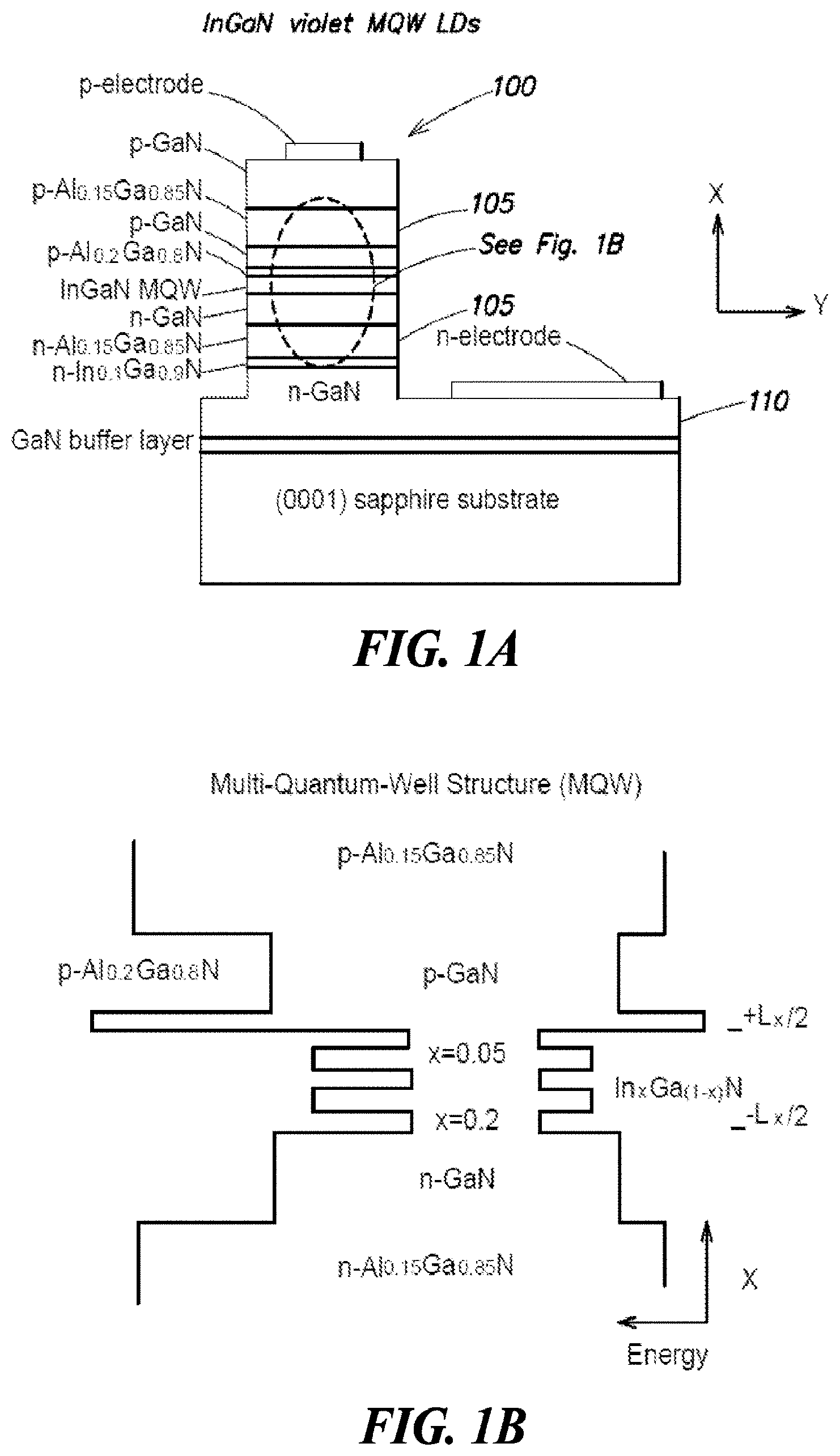
FIG. 1A depicts an elevation view of a semiconductor laser diode structure, according to some embodiments;
FIG. 1B depicts an energy band diagram for a semiconductor laser diode, according to some embodiments;
FIG. 2A depicts epitaxial layers for forming a III-nitride laser diode with a porous cladding layer, according to some embodiments;
FIGS. 2B-2D depict structures associated with a method for forming a III-nitride laser diode with a porous cladding layer, according to some embodiments;
FIG. 3 is a scanning electron microscope (SEM) image showing a porous GaN layer;
FIG. 4 depicts an edge-emitting semiconductor laser diode in perspective view;
according to some embodiments;
FIG. 5 illustrates optical mode confinement for waveguide structures cladded with non-porous AlGaN and porous GaN cladding layers;
FIGS. 6A and 6B illustrate optical mode confinement for two different structures and refractive index profiles;
FIG. 7 depicts a three-dimensional plot of confinement factor .GAMMA..sub.1D as a function of refractive index contrast and waveguide thickness. The dashed line indicates a higher confinement factor for a selected index contrast and preferred waveguide thickness;
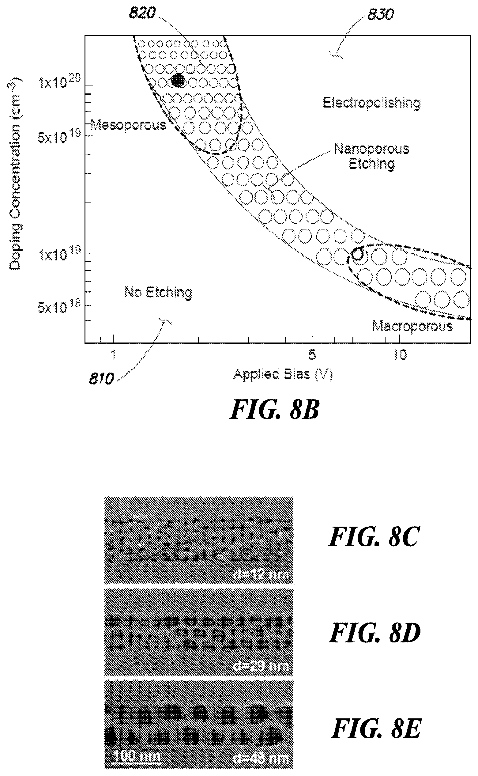
FIG. 8A and FIG. 8B depict electrochemical etching conditions, according to some embodiments;
FIGS. 8C-8E are SEM images showing nanoporous GaN formed under different electrochemical etching conditions; and
FIG. 9 shows stimulated emission from optically-pumped, edge-emitting, semiconductor lasers having porous cladding layers.
Features and advantages of the illustrated embodiments will become more apparent from the detailed description set forth below when taken in conjunction with the drawings.
DETAILED DESCRIPTION
The inventors have recognized and appreciated that conventional III-nitride edge-emitting laser diodes, as well as edge-emitting laser diodes fabricated in other semiconductor materials (e.g., GaAs, InP, etc.), have solid semiconductor cladding layers (e.g., formed of AlGaN for a III-nitride system) that limit the refractive index contrast between the active region and cladding layers of the laser diodes. This limit in refractive index contrast means that the optical mode for the laser is often not well confined and spatially does not match well to the diode's active region (the region where stimulated emission occurs). As a result, the inventors have recognized and appreciated that the diode's efficiency is not as high as it could be.
For example, III-nitride semiconductor laser diodes may comprise an SCH structure, like that of GaAs laser diodes. III-nitride laser diode structures may be grown on a GaN substrate or on a GaN template such as sapphire. AlGaN alloys (which have lower refractive index than GaN) may be grown in an epitaxial structure as the cladding layers, as depicted in FIG. 1A. The depicted laser diode structure 100 may be a conventional structure having two AlGaN cladding layers 105 (e.g., the two Al.sub.0.15Ga.sub.0.85N layers). The inventors have recognized and appreciated that for III-nitride structures, there is a large lattice mismatch between AN and GaN that can significantly limit the freedom of the laser design compared to the lattice matched AlAs and GaAs in a III-arsenide laser structure.
To improve the optical confinement in the active region for a III-nitride laser, higher index contrast (.DELTA.n=n.sub.activeregion-n.sub.cladding) is preferred between the active region and cladding. Since the refractive index of AlGaN decreases with increasing Al ratio, higher Al ratio in the AlGaN cladding layer is needed for higher index contrast (.DELTA.n=n.sub.GaN.times.n.sub.AlGaN). Preferably, .DELTA.n needs to be at least 0.05. However, because of the lattice size decrease with increasing Al ratio in the AlGaN ternary crystal, the increasing lattice mismatch of the AlGaN epitaxial layer to the GaN layer induces increasing tensile strain on GaN. Excessive buildup of such strain can lead to numerous problems including macroscopic epitaxial structure bowing and cracking, and microscopic creation of misfit dislocations and V-shaped morphological defects when grown past a certain (critical) thickness. All these problems can be detrimental to the performance and reliability of the laser diode.
In practice, conventional Al compositions of AlGaN cladding layers have been in a range from 5% to 20% in UV, blue, and green laser diodes. This range of values produces a .DELTA.n of roughly 0.02 to 0.08 for AlGaN-cladded III-nitride laser diodes, which only marginally fulfills requirement for refractive index contrast. Because of the low index contrast, the optical confinement factor is only around 2% to 3% for III-nitride diode lasers, even with active regions increased to several hundreds of nanometers thick and cladding layers that are several microns thick. For reference, a one-dimensional confinement factor (.GAMMA..sub.1D), for purposes of calculations and numerical results described below, may be expressed as:
.GAMMA..times..intg..times..function..times..intg..infin..infin..times..f- unction..times. ##EQU00001## where E(x) is the electric field amplitude for the optical mode in the x-direction. The mode confinement is roughly depicted as a dashed ellipse in FIG. 1A. The region having optical gain in the laser diode, where stimulated emission occurs (approximately equal to the region occupied by the multiple quantum wells), extends between .+-.L.sub.x/2.
A low transverse optical mode confinement in the x direction in FIG. 1A can cause a significant fraction of laser radiation to leak through the substrate and excite a substrate mode. Because an evanescent tail of the optical mode in the cladding layer may not decay abruptly, some fraction of the laser cavity mode can propagate into a thick n-type GaN layer 110 that underlies the laser heterostructure. Due to its high refractive index, the underlying GaN layer 110 can form a second parasitic waveguide, causing a significant leak of radiation from the active region and degradation of the transverse far-field pattern for the laser diode. As a result, the transverse mode can become a higher-order mode associated with the entire epitaxial structure 100. Such a mode shares its intensity with the thick GaN lateral contact layer underlying the laser heterostructure in which there is no optical gain, contributing to loss and reduced efficiency of the device.
To reduce the effect of the parasitic waveguide, the thickness of the cladding layer may be made sufficiently larger than the lateral expanse of the guided wave to reduce mode loss into the parasitic waveguide. For example, a group from Nichia Chemical reports using a very thick (5 .mu.m thick) Al.sub.0.05Ga.sub.0.095N:Si bottom-side cladding layer. Osram OS reports suppression of substrate modes by increasing the thickness of the bottom-side cladding layer to 2 .mu.m. To grow such thick AlGaN cladding layers without cracking, superlattice structures are needed that can better resist cracking for thicker layers. However, even with the complexity of these diode designs and superlattice epitaxy, the optical confinement factor remains below about 5%.
The inventors have also recognized and appreciated that an additional problem with AlGaN cladding is its conductivity, and also the conductivity for thick p-type doped GaN layers. Due to a deep level of Mg acceptor and low hole mobility in GaN, p-type GaN is of two orders of magnitude more resistive than Si-doped n-type GaN and still remains a bottleneck for III-nitride solid-state lighting. It has been reported that doping AlGaN with Mg is even less efficient than GaN, due to a difficulty in doping AlGaN. Thick cladding layers, required by low index contrast, and high resistivity will make the overall laser diode a more highly resistive electronic structure and less efficient, since a portion of the electrical current will be lost in ohmic heating of the resistive layers. The inventors have recognized and appreciated that AlGaN cladding layers in III-nitride lasers can adversely limit both optical confinement and electrical efficiency of a III-nitride laser diode.
To overcome limitations of solid AlGaN cladding layers, the inventors have conceived and developed methods and structures for forming porous cladding layers in III-nitride, edge-emitting laser diodes. The porous cladding layers can provide a high refractive index contrast and lower resistivity than conventional cladding layers. As a result, the porous layers can improve the confinement factor, the electrical efficiency, and overall emission efficiency of III-nitride, edge-emitting laser diodes. Porous cladding layers may also be used in edge-emitting laser diodes fabricated from other semiconductor materials. The inventors have also recognized and appreciated that efficient laser diodes may be useful high-intensity light sources instead of light-emitting-diodes (LEDs), because laser diodes emit light via stimulated emission which can avoid a phenomenon of "efficiency droop" that hampers performance of LEDs that emit light via spontaneous emission. Fabrication of an edge-emitting III-nitride laser diode with a nanoporous cladding layer will now be described.
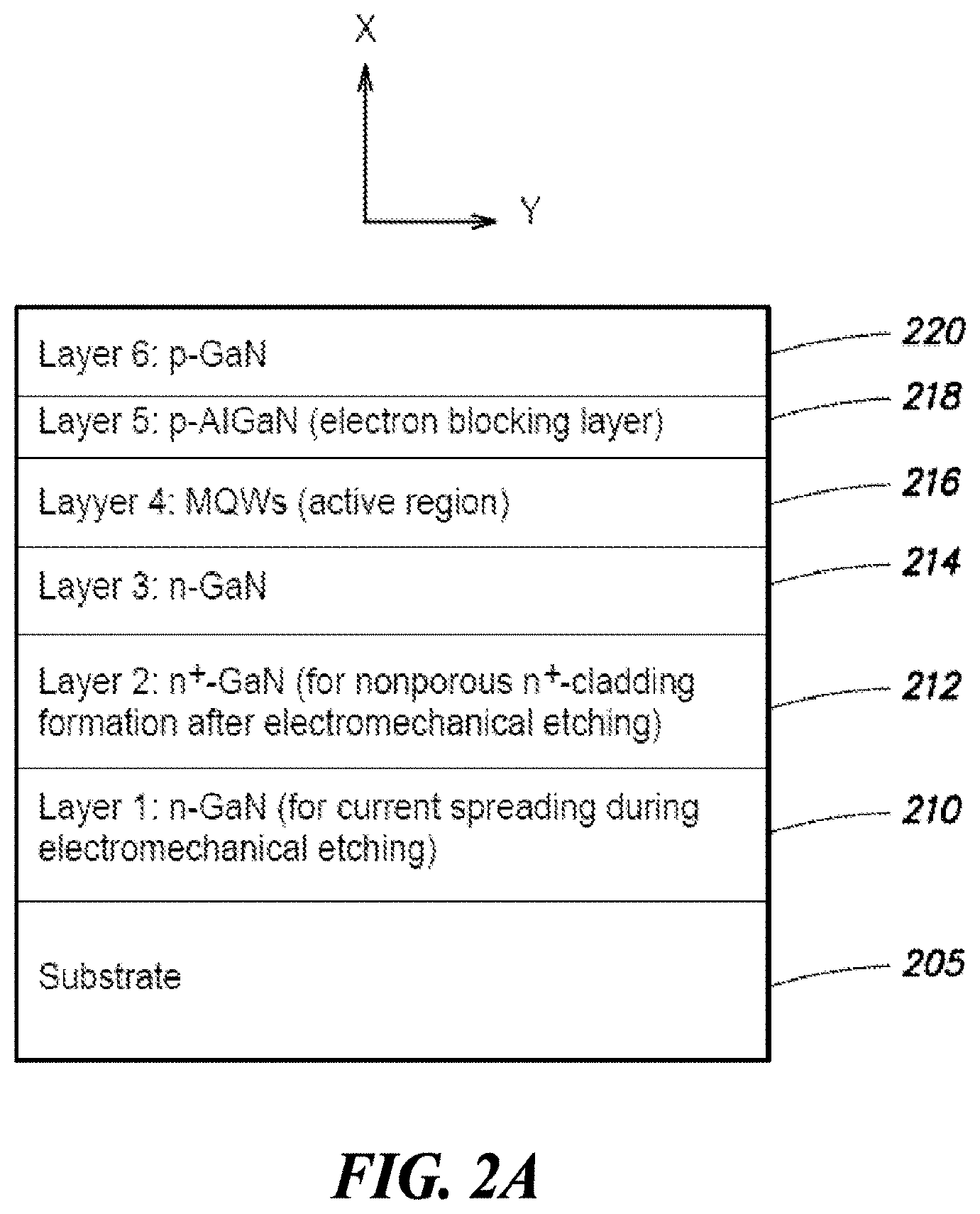
According to some embodiments, a multi-layered semiconductor structure, as depicted in FIG. 2A, may be grown by metal organic chemical vapor deposition (MOCVD) or metal organic vapor phase epitaxy. An active region 216 may be sandwiched in a waveguide structure that includes n-type 214 and p-type 220 layers. In some embodiments, the active region may comprise multiple quantum wells (MQWs) as depicted. In other embodiments, the active region may comprise a depletion region of a p-n junction. A thin (10.about.20 nm) AlGaN electron-blocking layer 218 may be formed between the active region 216 and p-type layer 220 to improve electron confinement in the active region where recombination and photon emission occurs. The layers between and including n-type 214 and p-type 220 layers may comprise an active junction of the device. An n-type GaN layer 210 having a doping level varying from about 1.times.10.sup.18 cm.sup.-3 to about 5.times.10.sup.18 cm.sup.-3 may provide electrical current spreading across an adjacent n.sup.+-type layer 212 during electrochemical etching of the adjacent layer and during device operation. In some cases, layer 210 may not be included. The n+-GaN layer 212 may be highly doped from about 5.times.10.sup.18 cm.sup.-3 to about 2.times.10.sup.20 cm.sup.-3 or above, so that electrochemical etching will produce a desirable nanoporous structure. In some implementations, the doping concentration of the n.sup.+-GaN layer 212 is at least a factor of 5 greater than the doping concentration of the n-GaN layer 210, so that the electrochemical etch will selectively etch the n.sup.+-GaN layer and not appreciably etch the n-GaN layer. Germanium (Ge) and/or silicon (Si) may be used as an n-type dopant for the n-type layers. A thickness of the n.sup.+-GaN layer 212 may be between about 200 nm and about 500 nm.
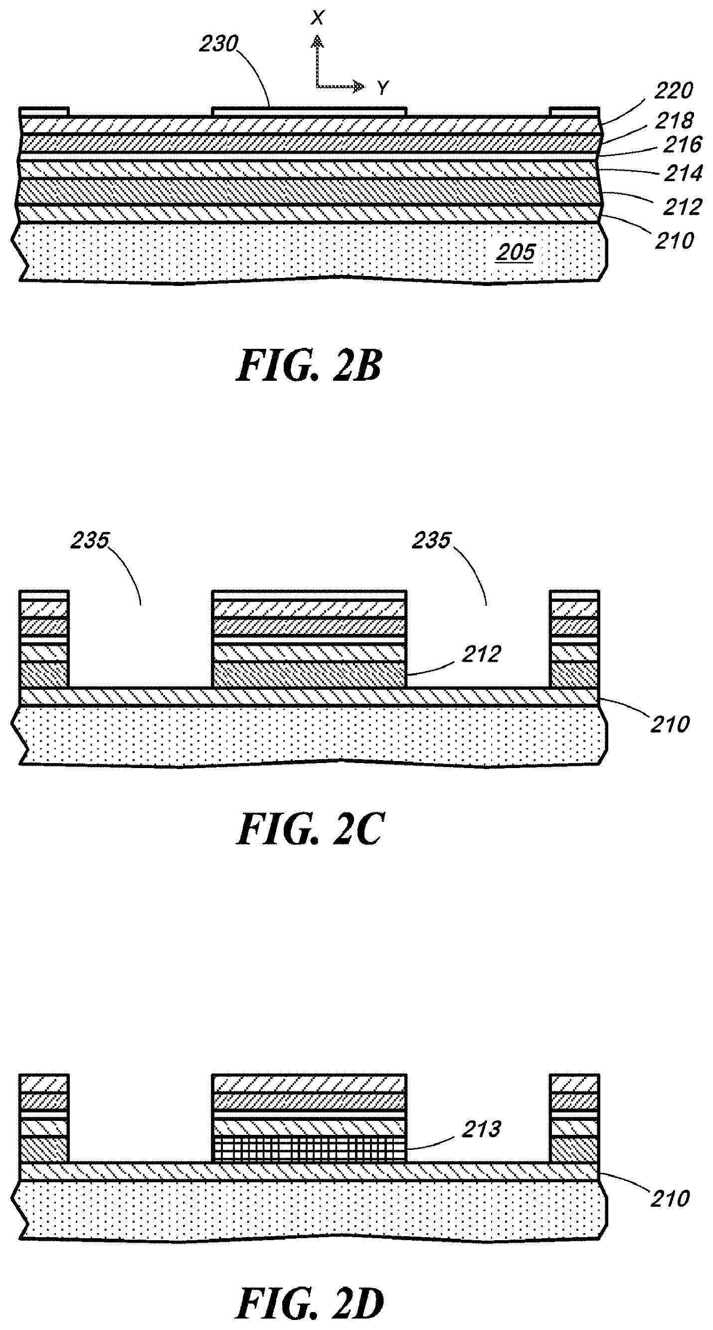
To electrochemically etch the n.sup.+-GaN layer, trenches may be etched into the epitaxial layers depicted in FIG. 2A or a mesa may be formed. The trenches may define a strip or bar-like structure for a laser cavity and expose sidewalls of the n.sup.+-GaN layer 212. In some embodiments, the etching of trenches may define lateral confinement for an optical mode in the y direction. In other embodiments, a rib structure may be formed on top of the stack to define lateral confinement for an optical mode in the y direction.
To form trenches, an oxide layer (e.g., SiO.sub.2) may be deposited by plasma-enhanced chemical vapor deposition (PECVD) or any other suitable process over the stack. Other hard mask layer materials may be used in some embodiments. A pattern for the laser cavity may be transferred to the oxide layer using standard photolithography and wet or dry etching to create a hard mask 230, as depicted in FIG. 2B. The mask pattern may then be transferred to the stack using any suitable dry etching process for GaN. For example, a Cl-based, inductively-coupled plasma (ICP) etching process may be employed to selectively remove III-nitride layers to form trenches 235. The dry etching may be timed so that the etch depth extends into the n.sup.+-GaN cladding layer 212 and exposes portions of the layer. The exposed portions of the n.sup.+-GaN cladding layer 212 may then be subsequently etched via an electrochemical etching process. In some embodiments, the trenches 235 may extend at least to a bottom of the n.sup.+-GaN cladding layer 212. On the other hand, the dry etching depth may not extend beyond the n-type layer 210, so that etching current can be spread across the whole wafer by layer 210 during the electrochemical etching. The etched structure may appear as depicted in FIG. 2C.
After the trenches 235 are formed, electrochemical (EC) etching may be performed to form a nanoporous n.sup.+-GaN cladding layer 213, as depicted in FIG. 2D. The experimental set-up for electrochemical etching may comprise a set-up described in U.S. patent application Ser. No. 13/559,199, filed Jul. 26, 2012, which is incorporated herein by reference. The EC etching does not require optical radiation for etching GaN, as is the case for photoelectrochemical (PEC) etching. EC etching, according to the present embodiments, may comprise using highly concentrated nitric acid (HNO.sub.3) at room temperature as the electrolyte. The concentration of the nitric acid may be between approximately 15 M and 18 M. In some embodiments, the nitric acid concentration is approximately 16.7 M or 70% by weight. The EC etching bias may be between 1 volt and 10 volts. The EC etching may laterally proceed into the n.sup.+-GaN cladding layer 212 and continue until the layer becomes a porous layer 213, as indicated in FIG. 2D. The EC etch may be a timed etch. The mask 230 may be stripped from the wafer.
In other embodiments, other electrolytes may be used to porosify the n.sup.+-GaN cladding layer 212. Other electrolytes include, but are not limited to, concentrated hydrofluoric acid, hydrochloric acid, sulfuric acid, and oxalic acid. Etchant concentrations, GaN doping, and bias voltages may be different for these etchants.
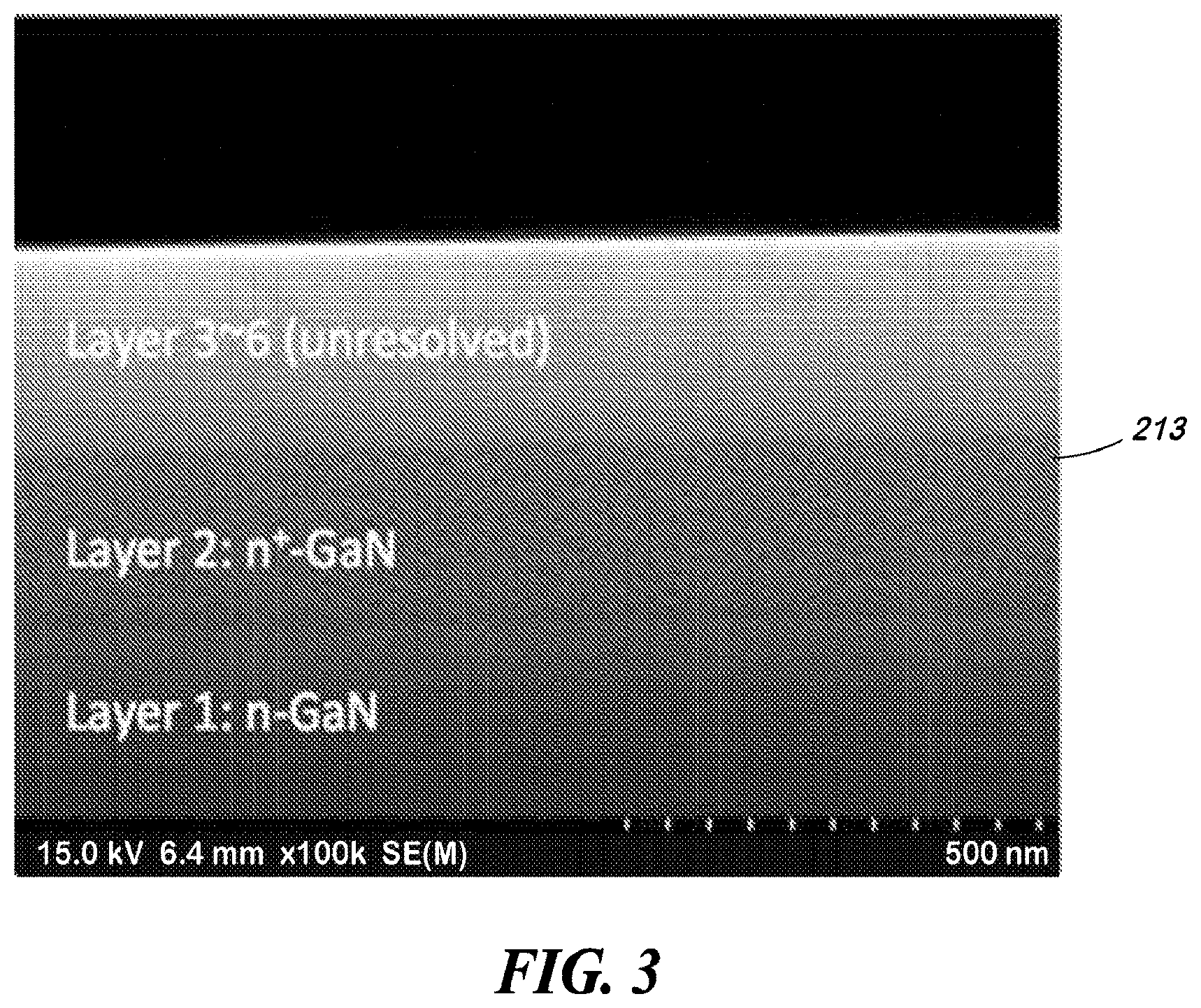
FIG. 3 is a scanning electron microscope (SEM) image showing a porosified n.sup.+-GaN cladding layer 213 after electrochemical etching. The pores appear as dark spots and are distributed uniformly throughout the layer. By controlling the doping level of the n.sup.+-GaN layer 212, etchant concentration, and etching bias, the EC etching may controllably produce nanoscale pores (e.g., pores having an average diameter value that is between about 10 nm and about 100 nm in some embodiments, and between about 10 nm and about 40 nm in some cases). When the pore diameters are appreciably less than the wavelength of light in the medium and uniformly distributed, the pores can alter the effective refractive index of the medium rather than act as scattering sites. For blue and green-wavelength laser diodes, it may be desirable to have an average pore diameter less than about 40 nm in a porous cladding layer. Additionally, controlling the doping level, etchant concentration, etching bias, and etching time, the EC etching may controllably produce a desired porosity of the structure. The term "porosity" is used to refer to a ratio of void or pore volume in a layer to a total volume occupied by the porous layer.
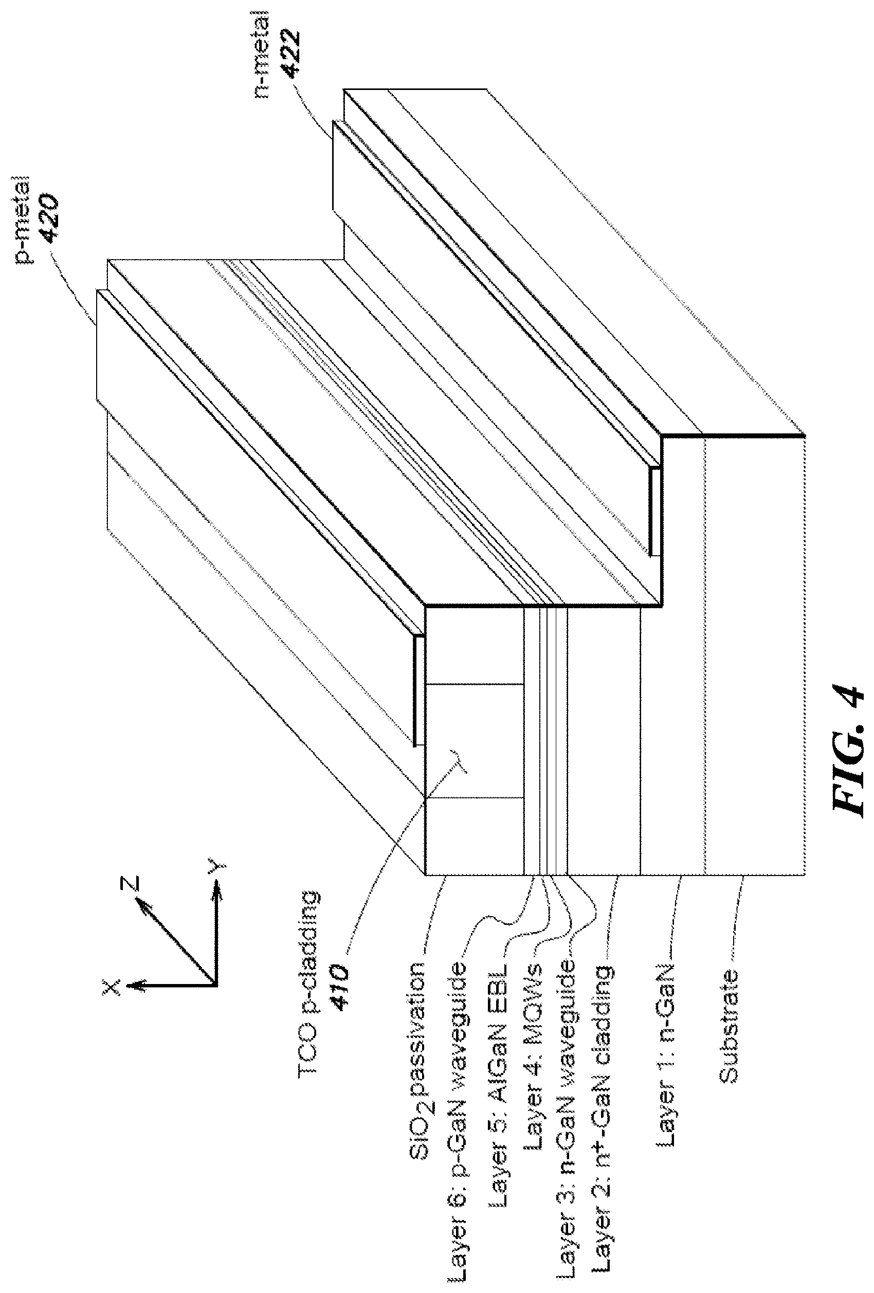
In some embodiments, a transparent conductive oxide (TCO) may be deposited to form a p-type cladding layer 410, as depicted in FIG. 4. The TCO may comprise indium tin oxide (ITO), which has lower resistivity than p-type AlGaN. A passivation layer (e.g., an insulating oxide such as SiO.sub.2) and contact pads 420, 422 may be added using conventional semiconductor manufacturing processes. In some embodiments, a passivation layer may be deposited prior to forming the contact pads, and vias may be opened in the passivation layer to make electrical contact with the laser diode.
The use of porous GaN and a TCO can eliminate the need for AlGaN cladding layers in a III-nitride laser diode structure. A porous GaN cladding layer may have several advantages over AlGaN cladding layers, as noted above. For example, a porous GaN layer can allow a high index contrast between the laser diode's active region 216 and porous cladding layer compared to a .DELTA.n of only about 0.02.about.0.08 when using AlGaN cladding. In some embodiments, the index contrast may be greater than about 0.5 (.DELTA.n.gtoreq.0.5). In some implementations, .DELTA.n.gtoreq.0.2. In some implementations, .DELTA.n.gtoreq.0.1. Additionally, the porosified n.sup.+-GaN layer is lattice matched to the adjacent layer, so that no significant material stress accumulates in the structure during epitaxial growth of the layers. Additionally, the porous n.sup.+-GaN layer can exhibit a lower resistivity than conventional AlGaN cladding layers.
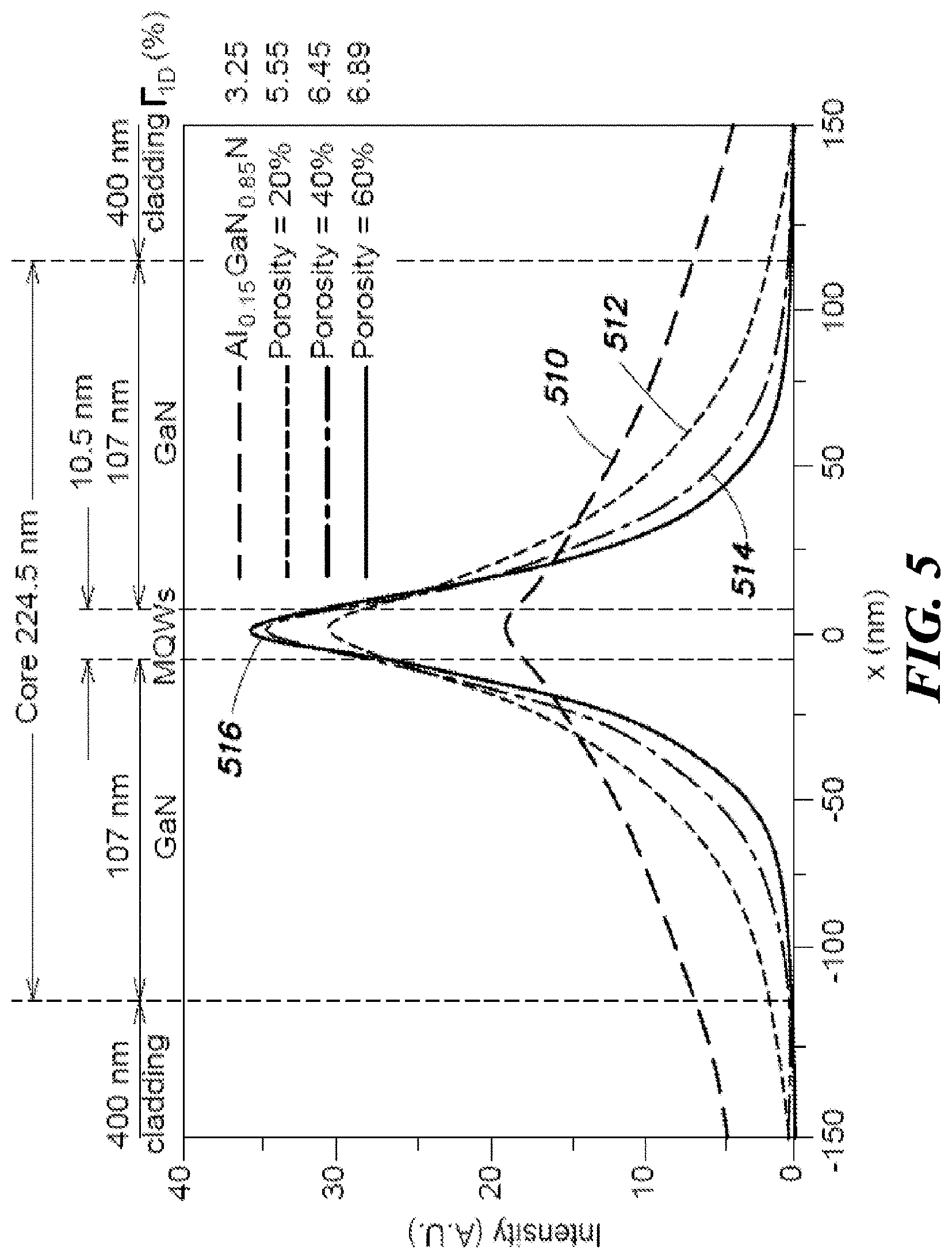
Analytical calculations were carried out to study the effect of cladding layer porosity on optical confinement, and to compare mode confinement against conventional devices with AlGaN cladding layers. Numerical results from these calculations are plotted in FIG. 5, FIG. 6A, and FIG. 6B. For the calculations, a structure of the laser diode comprises two semiconductor layers 214, 220 about 107 nm thick and an active region 216 about 10 nm thick. The cladding layers are each about 400 nm thick. The calculations are made for four different cladding layers: AlGaN (curve 510), 20% porous GaN (curve 512), 40% porous GaN (curve 514), and 60% porous GaN (curve 516). Changing from AlGaN to a 20% porous GaN cladding layer increases the mode confinement factor .GAMMA..sub.1D by nearly a factor of 2. As the porosity is increased, the optical mode becomes more tightly confined within the waveguide structure.
In terms of resistivity, the inventors have found through measurements that resistivity of nanoporous GaN scales monotonically with the porosity. After EC etching, the porous layer 213 may still have a doping concentration between about 1.times.10.sup.18 cm.sup.-3 and about 1.times.10.sup.19 cm.sup.-3. Since the n.sup.+-GaN cladding layer may be initially doped above 5.times.10.sup.19 cm.sup.-3 before porosification, even with a porosity of 40% the carrier concentration level of the nanoporous layer remains above 2.times.10.sup.18 cm.sup.-3. Such a high carrier concentration yields a negligible resistivity for the porous GaN cladding (compared to conventional n-AlGaN cladding), while the index contrast .DELTA.n can be tuned to as high as 0.5. In some implementations, the porosity of the n.sup.+-GaN cladding layer 213 is controlled via EC etching to be between about 30% and about 60%.
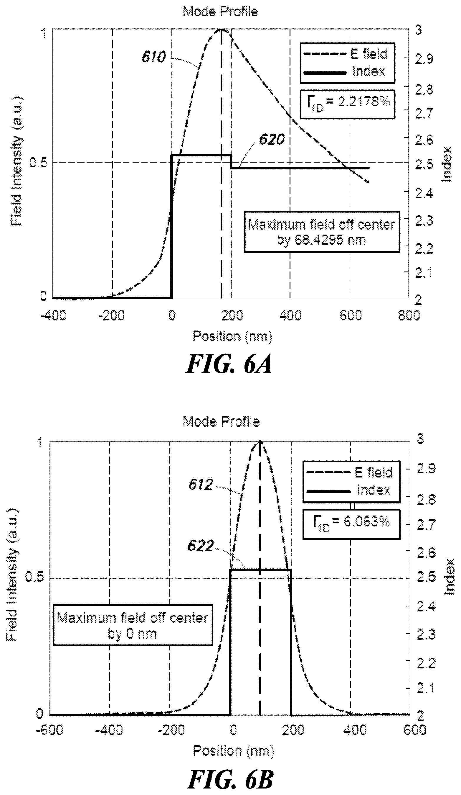
With a high index contrast between the n-GaN semiconductor layer 214 and the porous cladding layer 213, it is desirable to include a low index material as a p-type cladding layer to achieve a symmetrical mode profile in the laser diode and improved optical performance. According to some embodiments, a transparent conductive oxide such as ITO with a high index contrast to GaN (.DELTA.n.about.0.5) can be used to replace a highly resistive and low-.DELTA.n AlGaN p-type cladding. Although ITO has been proposed and used as a cladding layer for GaN laser diodes, its use without a porous bottom-side cladding layer can result in a highly asymmetric optical mode 610, as illustrated in FIG. 6A. In this structure, a substantial portion of the optical mode leaks outside the central waveguide region of the laser diode, where it will not experience optical gain. Also, a thick p-GaN layer 220 is still required adjacent the MQW active region to help reduce the asymmetry of the optical mode.
FIG. 6B shows improved optical mode confinement for an ITO p-side cladding layer and a nanoporous GaN n-side cladding layer. The porosity of the GaN layer is about 40%. The graph shows an approximately symmetric mode profile 622, centered at the active region. The confinement factor .GAMMA..sub.1D is increased from about 2.22% for the case illustrated in FIG. 6A to about 6.06%. For reference, the refractive index values are plotted as segmented lines 620, 622 in the two graphs.
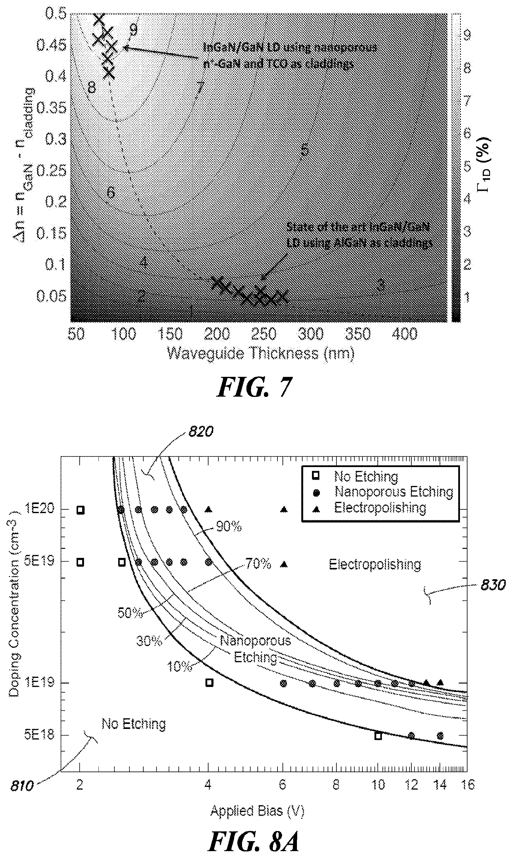
Numerical simulations were also carried out to plot the confinement factor .GAMMA..sub.1D with varying index contrast and waveguide thickness. The results are depicted in the three-dimensional plot of FIG. 7. The plot includes iso-contours for different values of the confinement factor. The dashed line represents preferred values of waveguide thickness for any given index contrast. With an index contrast of 0.05, a preferred waveguide thickness yields a confinement factor .GAMMA..sub.1D of only about 3%. For reference, conventional laser-diode structures with different .DELTA.n values and waveguide thicknesses are marked near the bottom of the graph with crosses. The confinement factors for these conventional devices are all in the 2% to 4% range.
The use of a nanoporous, bottom-side or substrate-side cladding layer and conductive oxide top-side cladding layer can enable an index contrast of up to 0.5 on both sides of the laser-diode active region and yield a one-dimensional confinement factor greater than 9%, in some embodiments. The crosses near the top left of the graph show confinement factor values for different device structures that use nanoporous GaN and conductive oxide cladding layers. For these structures, the confinement factor has increased by more than a factor of two. In addition to better mode confinement, the preferred waveguide thickness is also reduced by more than a factor of two. The reduction in waveguide thickness, notably for the resistive p-type GaN waveguide layer, will lower the serial resistance of the laser diode and further improve the device performance.
Further details of EC etching are illustrated in FIGS. 8A-8E. For the graphs of FIG. 8A and FIG. 8B, a concentrated nitric acid (between 15M and 17M) is used as the electrolyte. Etching is performed at room temperature and under potentiostatic (constant voltage) bias. When a positive anodic bias is applied to an n.sup.+-type GaN sample immersed in an acidic electrolyte, the n.sup.+-GaN can become oxidized by holes at a surface inversion layer. The surface oxide layer is subsequently dissolved by the electrolyte. When the applied bias and/or the doping concentration is low, no chemical reactions occur and the n.sup.+-GaN remains unetched. The region 810 of no etching is depicted at the lower left of the graphs. As the applied bias and/or the doping concentration increases, electrostatic breakdown occurs with the injection of holes to certain localized hot spots. This results in the formation of nanoporous structures, and is indicated by a curved central nanoporous region 820 in the graphs. At an even higher applied bias and/or with higher doping concentration, electro-polishing (complete etching) takes place and is indicated by the region 830 to the upper right in the graphs.
Within the nanoporous region 820, the inventors have found that the pore morphology can be controlled by the sample conductivity and the anodic bias. A higher doping level facilitates the formation of high curvature and smaller meso-pores, and the threshold bias of porosification is reduced accordingly. Tunability of pore morphology is illustrated in FIG. 8B and FIGS. 8C-8E. By varying the doping concentration of an n.sup.+-GaN cladding layer from about 1.times.10.sup.20 cm.sup.-3 to about 1.times.10.sup.19 cm.sup.-3 and varying the EC etching bias between about 1 volt and about 12 volts, the resulting pore morphology can be varied from microporous (average pore diameter d.about.10 nm, FIG. 8C) to mesoporous (d.about.30 nm, FIG. 8D), and to macroporous (d.about.50 nm, FIG. 8E). Further, for a given doping concentration, the EC bias can be adjusted to alter the percent porosity of the cladding layer, as is depicted by the contour lines in the nanoporous region 820 of FIG. 8A.
Although the embodiments described above refer to electrically pumped laser diodes, the formation and use of porous cladding layers may be extended to optically-pumped, edge-emitting, semiconductor lasers or optical amplifiers. An optically-pumped device may be formed in the same way, although the top p-type GaN layer 220 may be replaced with a second n-type GaN layer 214, referring to FIG. 2A. The device may then be pumped with another laser or suitable optical source to create a population inversion in the MQW active region 216.
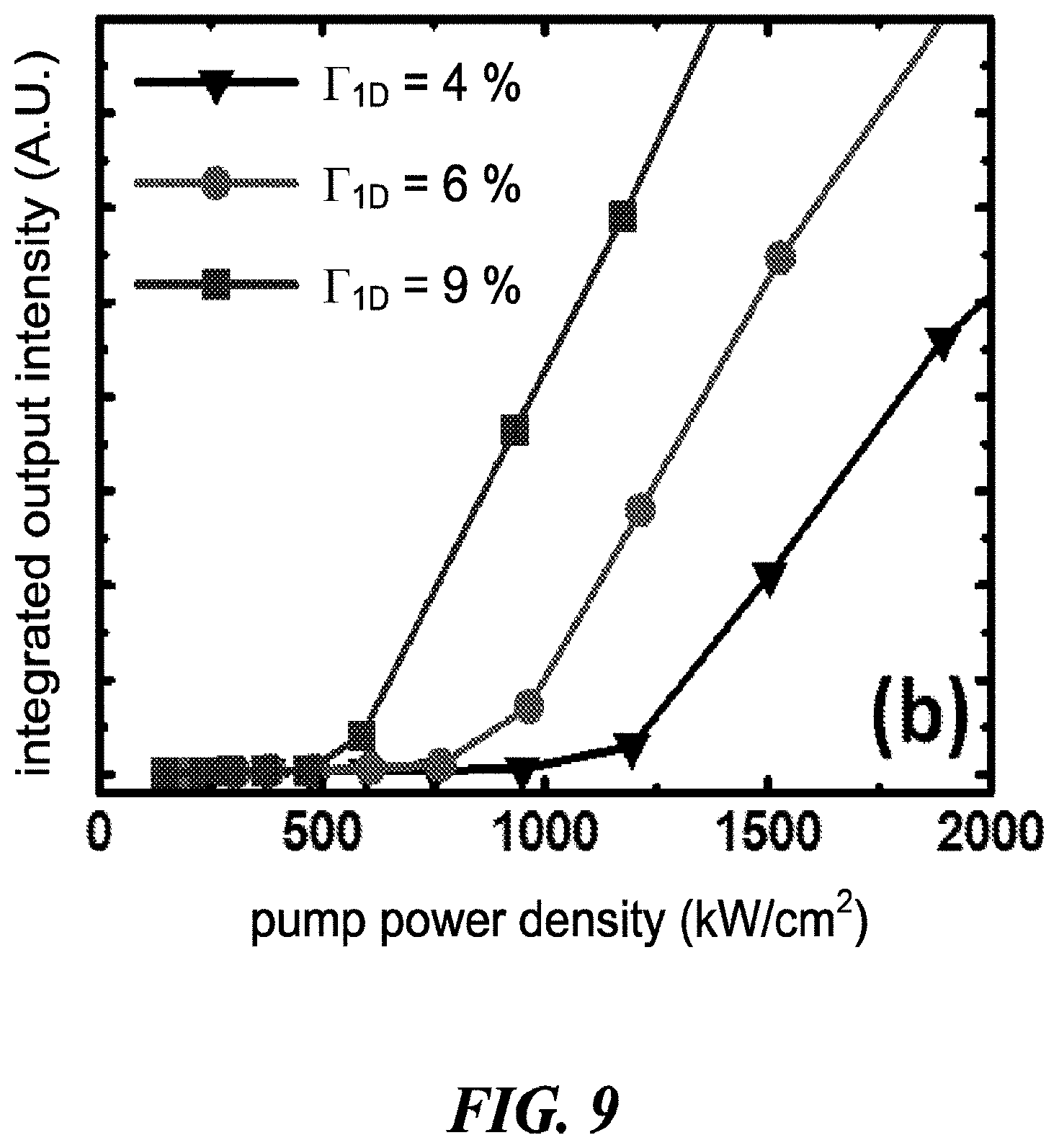
FIG. 9 shows stimulated emission from optically-pumped, edge-emitting, semiconductor lasers with porous cladding layers and having three different confinement factors. The integrated output intensity from the lasers are plotted as a function of optical pump power density delivered to the lasers. The curves show distinct threshold behavior for the three lasers. The threshold values reduce for increased confinement factors.
Nanoporous GaN cladding layers can be used to obtain high index contrast for cladding layers in edge-emitting III-nitride diode lasers, without problems of material stress and resistivity associated with AlGaN cladding layers. The nanoporous GaN cladding layers may be formed from layers grown using metal-organic epitaxial growth conditions, and may be formed in standard III-nitride epitaxial growth systems without significantly altering the growth processes. The porosification of a bottom-side cladding layer and deposition of a top-side TCO cladding layer may be performed after epitaxy, so that these acts will neither induce extra epitaxial constraints nor contribute to defect generation in the epitaxial layers. In some implementations, the fabrication steps may include conventional III-nitride device processes that can be applied in existing chip fabrication facilities. For example, electrochemical etching to form a porous III-nitride cladding layer can be an inexpensive and environmental-friendly technique. It may be conducted in existing chip fabrication facilities, and is compatible with high-volume production.
Numerical values and ranges may be given in the specification and claims as approximate values or exact values. For example, in some cases the terms "about," "approximately," and "substantially" may be used in reference to a value. Such references are intended to encompass the referenced value as well as plus and minus reasonable variations of the value. For example, a phrase "between about 10 and about 20" is intended to mean "between exactly 10 and exactly 20" in some embodiments, as well as "between 10.+-..delta.1 and 20.+-..delta.2" in some embodiments. The amount of variation .delta.1, .delta.2 for a value may be less than 5% of the value in some embodiments, less than 10% of the value in some embodiments, and yet less than 20% of the value in some embodiments. In embodiments where a large range of values is given, e.g., a range including two or more orders of magnitude, the amount of variation .delta.1, .delta.2 for a value could be 50%. For example, if an operable range extends from 2 to 200, "approximately 80" may encompass values between 40 and 120.
The technology described herein may be embodied as a method, of which at least some acts have been described. The acts performed as part of the method may be ordered in any suitable way. Accordingly, embodiments may be constructed in which acts are performed in an order different than described, which may include performing some acts simultaneously, even though described as sequential acts in illustrative embodiments. Additionally, a method may include more acts than those described, in some embodiments, and fewer acts than those described in other embodiments.
Having thus described at least one illustrative embodiment of the invention, various alterations, modifications, and improvements will readily occur to those skilled in the art. Such alterations, modifications, and improvements are intended to be within the spirit and scope of the invention. Accordingly, the foregoing description is by way of example only and is not intended as limiting. The invention is limited only as defined in the following claims and the equivalents thereto.
* * * * *
D00000
D00001
D00002
D00003
D00004
D00005
D00006
D00007
D00008
D00009
D00010
M00001
XML
uspto.report is an independent third-party trademark research tool that is not affiliated, endorsed, or sponsored by the United States Patent and Trademark Office (USPTO) or any other governmental organization. The information provided by uspto.report is based on publicly available data at the time of writing and is intended for informational purposes only.
While we strive to provide accurate and up-to-date information, we do not guarantee the accuracy, completeness, reliability, or suitability of the information displayed on this site. The use of this site is at your own risk. Any reliance you place on such information is therefore strictly at your own risk.
All official trademark data, including owner information, should be verified by visiting the official USPTO website at www.uspto.gov. This site is not intended to replace professional legal advice and should not be used as a substitute for consulting with a legal professional who is knowledgeable about trademark law.