Nanolaminated 2-2-1 MAX-phase compositions
Barsoum , et al. Ja
U.S. patent number 10,538,431 [Application Number 15/554,904] was granted by the patent office on 2020-01-21 for nanolaminated 2-2-1 max-phase compositions. This patent grant is currently assigned to Drexel University. The grantee listed for this patent is Drexel University. Invention is credited to Michel W. Barsoum, Chunfeng Hu.
| United States Patent | 10,538,431 |
| Barsoum , et al. | January 21, 2020 |
Nanolaminated 2-2-1 MAX-phase compositions
Abstract
The present invention is directed to crystalline solids having an empirical formula of M.sub.2A.sub.2X, wherein M is at least one Group IIIB, IVB, VB, or VIB metal, preferably Cr, Hf, Sc, Ti, Mo, Nb, Ta, V, Zr, or a combination thereof; wherein A is Al, Ga, Ge, In, Pb, or Sn, or a combination thereof; and each X is C.sub.xN.sub.y, where x+y=1. In some particular embodiments, the crystalline composition has a unit cell stoichiometry of Mo.sub.2Ga.sub.2C.
| Inventors: | Barsoum; Michel W. (Moorestown, NJ), Hu; Chunfeng (Philadelphia, PA) | ||||||||||
|---|---|---|---|---|---|---|---|---|---|---|---|
| Applicant: |
|
||||||||||
| Assignee: | Drexel University
(Philadelphia, PA) |
||||||||||
| Family ID: | 56848716 | ||||||||||
| Appl. No.: | 15/554,904 | ||||||||||
| Filed: | March 1, 2016 | ||||||||||
| PCT Filed: | March 01, 2016 | ||||||||||
| PCT No.: | PCT/US2016/020216 | ||||||||||
| 371(c)(1),(2),(4) Date: | August 31, 2017 | ||||||||||
| PCT Pub. No.: | WO2016/140948 | ||||||||||
| PCT Pub. Date: | September 09, 2016 |
Prior Publication Data
| Document Identifier | Publication Date | |
|---|---|---|
| US 20180044182 A1 | Feb 15, 2018 | |
Related U.S. Patent Documents
| Application Number | Filing Date | Patent Number | Issue Date | ||
|---|---|---|---|---|---|
| 62127907 | Mar 4, 2015 | ||||
| Current U.S. Class: | 1/1 |
| Current CPC Class: | C01B 32/90 (20170801); C01B 21/072 (20130101); C01B 21/0605 (20130101); C01B 21/0617 (20130101); C01B 21/062 (20130101); C01B 21/0632 (20130101); C01B 21/076 (20130101); C01B 21/0602 (20130101); H01M 4/58 (20130101); C01P 2002/72 (20130101) |
| Current International Class: | C01B 21/06 (20060101); C01B 21/072 (20060101); C01B 32/90 (20170101); C01B 21/076 (20060101); H01M 4/58 (20100101) |
References Cited [Referenced By]
U.S. Patent Documents
| 4801368 | January 1989 | Yamashita et al. |
| 6180049 | January 2001 | Jang et al. |
| 6555268 | April 2003 | Inoue et al. |
| 7446190 | November 2008 | Sadelain et al. |
| 2002/0068488 | June 2002 | Tuller et al. |
| 2003/0148184 | August 2003 | Omaru et al. |
| 2003/0224168 | December 2003 | Mack et al. |
| 2004/0048157 | March 2004 | Neudecket et al. |
| 2004/0229028 | November 2004 | Sasaki et al. |
| 2007/0065725 | March 2007 | Inoue |
| 2007/0066503 | March 2007 | Basaly |
| 2009/0017332 | January 2009 | Kisi et al. |
| 2010/0236937 | September 2010 | Rosvall et al. |
| 2010/0322909 | December 2010 | Okada et al. |
| 2011/0017585 | January 2011 | Zhamu et al. |
| 2011/0104464 | May 2011 | Pyzik et al. |
| 2012/0247800 | October 2012 | Shah et al. |
| 2013/0092428 | April 2013 | Kawaguchi et al. |
| 2014/0162130 | June 2014 | Barsoum et al. |
| 2015/0210044 | July 2015 | Barsoum et al. |
| 2015/0306570 | October 2015 | Mayes et al. |
| 0 948 067 | Oct 1999 | EP | |||
| 1 381 099 | Jan 2004 | EP | |||
| H08 78018 | Mar 1996 | JP | |||
| H10 112316 | Apr 1998 | JP | |||
| 2005 158725 | Jun 2005 | JP | |||
| 2007 214137 | Aug 2007 | JP | |||
| WO 2002/081372 | Oct 2002 | WO | |||
| WO 2002/096799 | Dec 2002 | WO | |||
| WO 2005/007566 | Jan 2005 | WO | |||
| WO 2006/112869 | Oct 2006 | WO | |||
| WO 2007/093011 | Aug 2007 | WO | |||
| WO 2007/093011 | Aug 2007 | WO | |||
| WO 2007/121931 | Nov 2007 | WO | |||
| WO 2009/063031 | May 2009 | WO | |||
| WO 2009/091826 | Jul 2009 | WO | |||
| WO 2010/128492 | Nov 2010 | WO | |||
| WO 2014/088995 | Jun 2014 | WO | |||
Other References
|
Hu et al.; Mo2Ga2C: a new ternary nanolanninated carbide; Chem. Commun., 51, 6560-6563; Mar. 2015. cited by examiner . Barsoum et al, "Room-Temperature Deintercalation and Self-Extrusion of Ga from Cr2GaN", Science, May 7, 1999, 284(5416), 937-939. cited by applicant . Barsoum et al, "The Topotactic Transformation of Ti3SiC2 into a Partially Ordered Cubic Ti(C0.67Si0.06) Phase by the Diffusion of Si into Molten Cryolite", Journal of the Electrochemical Society, 1999, 146(10), 3919-3923. cited by applicant . Barsoum, "Physical Properties of the MAX phases", Encyclopedia of Materials: Science and Technology, 2006, 11 pages. cited by applicant . Barsoum, et al., "Synthesis and Characterization of a Remarkable Ceramic: Ti3SiC2," J Amer. Chem. Soc., 1996 79(7), 1953-1956. cited by applicant . Barsoum, M. and El-Raghy, T., "The MAX Phases: Unique New Carbide and Nitride Materials", American Scientist, Jul.-Aug. 2001, 89:334-343. cited by applicant . Barsoum, M., "The MN+1AXN phases: New Class of Solids", Progress in Solid State Chemistry, Jan. 1, 2000, 28(1-4), 201-281. cited by applicant . Chang et al., "Synthesis of a new graphene-like transition metal carbide by de-intercalating Ti.sub.3AlC.sub.2", Mater. Lett., Oct. 2013, 109, 295-298. cited by applicant . Chen et al, "Microstructure and Phase Transformation of Ti 3 Ac 2 (A= Al, Si) in Hydrofluoric Acid Solution", Crystal Research and Technology, Oct. 27, 2014, 49(10), 813-819. cited by applicant . Chen et al., "In-situ synthesis of Ti3AlC2/TiC-A120O3 composite from TiO2--Al--C system", Journal of Materials Science & Technology, 2006, 22, 455-458. cited by applicant . Coleman et al, "Two-Dimensional Nanosheets Produced by Liquid Exfoliation of Layered Materials", Science, Feb. 4, 2011, 331, 568-571. cited by applicant . Eis, PS et al, Accumulation of miR-155 and BIC RNA in Human B Cell Lymphomas. Proceedings of the National Academy of Sciences of the United States of America, Mar. 8, 2005, 102(10), 3627-3632, Abstract. cited by applicant . Eklund et al, "The Mn+1AXn Phases: Materials Science and Thin-Film Processing", Thin Solid Films, 2010, 518, 1851-1878. cited by applicant . Ettmayer et al., "Crystal structure of Cr3(C,N)2 and CrVC2", Monatshefte fur Chemie and Verwandte Teile Anderer Wissenschaften, Jul. 1966, vol. 97, Issue 4, 1258-1262. cited by applicant . European Patent Application No. 12803351.1: Supplementary European Search Report dated Jan. 30, 2015, 14 pages. cited by applicant . Finkel et al., "Magnetotransport properties of the ternary carbide Ti3SiC2: Hall effect, magnetoresistance, and magnetic susceptibility", Physical Review B, Jan. 15, 2002, vol. 65, Issue 3, 4 pages. cited by applicant . Ghidiu et al., "Conductive two-dimensional titanium carbide `clay` with high volumetric capacitance", Nature, Dec. 2014, 516, 78-81. cited by applicant . Halim et al., "Transparent Conductive Two-Dimensional Titanium Carbide Epitaxial Thin Films", Chem. Mater., 2014, vol. 26, No. 7, 2374-2381, Abstract; p. 2376, Scheme 1, p. 2379, col. 1, para. 2; p. 2379, col. 2, para. 2. cited by applicant . Henadaoui et al., "Ti--Al--C MAX Phases by Aluminothermic Reduction process", International Journal of Self-Propagating High-Temperature Synthesis, 2008, 17, 125-128. cited by applicant . Hu et al. "Two-dimensional Sc.sub.2C: A reversible and high-capacity hydrogen storage material predicted by first principles calculations", International Journal of Hydrogen Energy, Jul. 2014, 39, 20, 10606-10612. cited by applicant . Hu et al., "MXene: A New Family of Promising Hydrogen Storage Medium", J. Phys. Chem A, 2013, 117, 14523-14260. cited by applicant . Hu, C., "Low Temperature Thermal Expansion, High Temperature Electrical Conductivity, and Mechanical Properties of Nb4AlC3 Ceramic Synthesized by Spark Plasma Sintering", Journal of Alloys and Compounds, Nov. 13, 2009, 487(1-2), 675-681. cited by applicant . International Patent Application No. PCT/US13/072733: The International Search Report and the Written Opinion dated Mar. 28, 2014, pp. 1-12. cited by applicant . International Patent Application No. PCT/US13/64503: The International Search Report and the Written Opinion dated Jan. 24, 2014, pp. 1-13. cited by applicant . Jin et al., "Synthesis of VC--Cr3C2 Nanocomposite Powders by Carbothermal Reduction", Nanoscience and Nanotechnology Letters, Oct. 2012, vol. 4, No. 10, 1028-1030, Abstract, 1 page. cited by applicant . Korzhavyi et al, "Ab Initio Study of Phase Equilibria in TiC.sub.x", Physical Review Letters, Dec. 18, 2001, 88(1), 1-4. cited by applicant . Kulkarni et al, Thermal Expansion and Stability of Ti2SC in Air and Inert Atmospheres, Journal of Alloys and Compounds, 2009, 469, 395-400. cited by applicant . Mogilevsky et al, "The Structure of Multilayered Titania Nanotubes Based on Delaminated Anatase", Chemical Physics Letters, 2008, 460, 517-520. cited by applicant . Myhra, et al., "Crystal-Chemistry of the Ti.sub.3AlC.sub.2 and Ti.sub.4AlN Layered Carbide/Nitride Phases--Characterization by XPS", Journal of Physics and Chemistry of Solids, Apr. 2001, vol. 62(4), 811-817. cited by applicant . Nadeau, "Clay Particle Engineering: a Potential New Technology with Diverse Applications", Applied Clay Science, 1987, 2, 83-93. cited by applicant . Naguib et al, "Mxene: A Promising Transition Metal Carbide Anode for Lithium-ion Batteries", Electrochemistry Communications, 2012, 16, 61-64. cited by applicant . Naguib et al, "New Two-dimensional Niobium and Vanadium Carbides as Promising Materials for Li-Ion Batteries", American Chemical Society, Oct. 2013, 135(43), 15966-15969. cited by applicant . Naguib et al, Synthesis of a New Nanocrystalline Titanium Aluminum Fluoride Phase by Reaction of Ti2aic With Hydrofluoric Acid, RSC Adv. 1: 1493-1499, 2011. [retrieved on Mar. 7, 2014]. Retrieved from the internet: <URL: http://pubs.rsc.org .ezproxy.neu.ed u/en/Content/Articlelanding/2011/RA/c1raO0390a#/div, Abstract. cited by applicant . Naguib et al, "Two-Dimensional Nanocrystals Produced by Exfoliation of Ti.sub.3AlC.sub.2", Advanced Materials, 2011, 23, 4248-4253. cited by applicant . Naguib et al, "Two-Dimensional Transition Metal Carbides", American Chemical Society, Feb. 2012, 6(2), 1322-1331. cited by applicant . Naguib et al., "Mxenes: A new family of two-dimensional materials", Advanced Materials, 2014, 26, 992-1005. cited by applicant . Nan et al., "Percolation phenomena in niobium-doped TiC1-x", Materials Science and Engineering B-Solid State Materials for Advanced Technology, Feb. 1991, vol. 7, Issue 4, 283-286. cited by applicant . Peng et al., "Unique lead adsorption behavior of activated hydroxyl group in two-dimensional titanium carbide", Journal of the American Chemical Society, 2014, 136, 4113-4116. cited by applicant . Rao et al, "A Study of the Synthetic Methods and Properties of Graphenes", Science and Technology of Advanced Materials, 11, Oct. 27, 2010, 1-15. cited by applicant . Rudy, "Crystal structure of Ta2VC2", Journal of the Less-Common Motale, Jan. 1970, vol. 20, Issue 1, 49-55. cited by applicant . Savoskin et al, "Carbon Nanoscrolls Produced From Acceptor-Type Graphite Intercalation Compounds", 2007, Carbon, 45, 2797-2800. cited by applicant . Schmidt, et al., "XPS Studies of Amino Acids Absorbed on Titanium Dioxide Surfaces", Fresenius Journal of Analytical Chemistry, May 1991, 341, 412-415. cited by applicant . Spanier et al, "Vibrational Behavior of the Mn+1AXn phases from First-Order Raman Scattering ,,M=Ti ,V,Cr, A=Si, X=C,N)", Physical Review B, Jan. 2005, 71, 1-4. cited by applicant . Srinivasan, "Batteries for Advanced Transportation Technologies (BATT) Program. The fourth quarter 2014 FY report", Berkeley National Laboratory Document, Nov. 19, 2014, http://bmr.lbl.gov/wp-content/uploads/sites/3battfiles/reports/BATT_2014_- 4th_Quarterly_Report.pdf, 74 pages. cited by applicant . Stankovich et al, "Graphene-based Composite Materials", Nature, Jul. 2006, 442, 282-286. cited by applicant . Su et al., "High-Quality Thin Graphene Films from Fast Electrochemical Exfoliation", ACS Nano, 2011, 5(3), 2332-2339. cited by applicant . Tang et al., "Are MXenes Promising Anode Materials for Li Ion Batteries? Computational Studies on Electronic Properties and Li Storage Capability of Ti.sub.3C.sub.2 and Ti.sub.3C.sub.2X.sub.2 (X=F, OH) Monolayer", Journal of the American Chemical Society, 2012, 134, 16909-16916. cited by applicant . Tran et al, "Lithium Intercalation in Porous Carbon Electrodes", Material Research Society 1995 Spring Meeting, San Francisco, CA, Apr. 17-21, 1995, 12 Pages. cited by applicant . Travaglini et al, "The Corrosion Behavior of Ti3SiC2 in Common Acids and Dilute NaOH", Corrosion Science, Jun. 1, 2003, 45(6), 1313-1327. cited by applicant . Tzenov et al, "Synthesis and Characterization of Ti3AlC2", Journal of the American Ceramic Society, Jan. 1, 2000, 83(4), 825-832. cited by applicant . Viculis et al, "A Chemical Route to Carbon Nanoscrolls", Science, Feb. 28, 2003, 299, p. 1361. cited by applicant . Viculis, et al., "Intercalation and Exfoliation Routes to Graphite Nanoplatelets", Journal of Materials Chemistry, 2005, vol. 15, 974-978. cited by applicant. |
Primary Examiner: Gregorio; Guinever S
Attorney, Agent or Firm: BakerHostetler
Government Interests
GOVERNMENT RIGHTS
This invention was made with government support under Contract No. DMR-1310245 awarded by the National Science Foundation. The government has certain rights in the invention.
Parent Case Text
CROSS-REFERENCE TO RELATED APPLICATIONS
This application is the National Stage Application of International Patent Application No. PCT/US2016/020216, filed Mar. 1, 2016, which claims priority to U.S. Patent Application Ser. No. 62/127,907, filed Mar. 4, 2015, the contents of which are incorporated by reference herein in their entireties for all purposes.
Claims
What is claimed:
1. A crystalline solid having an empirical formula of M.sub.2A.sub.2X, wherein M is Cr, Hf, Sc, Ti, Mo, Nb, Ta, V, Zr, or a combination thereof; wherein A is Al, Ga, Ge, In, Pb, or Sn, or a combination thereof; and each X is C.sub.xN.sub.y, where x+y=1.
2. The crystalline solid of claim 1 that is Cr.sub.2Ga.sub.2C, Cr.sub.2Ga.sub.2N, Mo.sub.2Ga.sub.2C, Mo.sub.2Ga.sub.2N, Nb.sub.2Ga.sub.2C, Nb.sub.2Ga.sub.2N, Ta.sub.2Ga.sub.2C, Ta.sub.2Ga.sub.2N, Ti.sub.2Ga.sub.2C, Ti.sub.2Ga.sub.2N, V.sub.2Ga.sub.2C, or V.sub.2Ga.sub.2N.
3. The crystalline solid of claim 1 that is Hf.sub.2In.sub.2C, Hf.sub.2In.sub.2N, Hf.sub.2Sn.sub.2C, Hf.sub.2Sn.sub.2N, Nb.sub.2In.sub.2C, Nb.sub.2In.sub.2N, Nb.sub.2Sn.sub.2C, Nb.sub.2Sn.sub.2N, Sc.sub.2In.sub.2C, Sc.sub.2In.sub.2N, Ti.sub.2In.sub.2C, Ti.sub.2In.sub.2N, Ti.sub.2Sn.sub.2C, Ti.sub.2Sn.sub.2N, Zr.sub.2In.sub.2C, Zr.sub.2In.sub.2N, Zr.sub.2Sn.sub.2C, or Zr.sub.2Sn.sub.2N.
4. The crystalline solid of claim 1, wherein the empirical formula is defined by the unit cell stoichiometry of the crystalline solid.
5. The crystalline solid of claim 1, having a unit cell stoichiometry of Mo.sub.2Ga.sub.2C.
6. The crystalline solid of claim 5, in which two layers of Ga atoms are stacked between otherwise adjacent Mo.sub.2C layers.
7. The crystalline solid of claim 5, wherein the Ga atoms are stacked in a simple hexagonal arrangement of atoms.
8. The crystalline solid of claim 1, wherein A is Ga, In, or Sn, and in which two layers of Ga, In, or Sn atoms are stacked between layers of Cr.sub.2C, Cr.sub.2N, Hf.sub.2C, Hf.sub.2N, Mo.sub.2C, Mo.sub.2N, Nb.sub.2C, Nb.sub.2N, Sc.sub.2C, Sc.sub.2N, Ta.sub.2C, Ta.sub.2N, Ti.sub.2C, Ti.sub.2N, V.sub.2C, V.sub.2N, Zr.sub.2C, or Zr.sub.2N.
9. The crystalline solid of claim 1 comprising molybdenum, gallium, and carbon exhibiting at least five of the following characteristic X-ray powder diffraction peaks (Cu K.alpha. radiation, expressed in degrees 2.theta.) at approximately 9.8, 34.1, 37.3, 39.9, 42.5, 53.4, 61.0, and 75.4 and optionally other one or more additional peaks at approximately 67.1, 73.7, 77.2, or 77.6 degrees 2.theta..
10. The crystalline solid of claim 1 consisting essentially of molybdenum, gallium, and carbon exhibiting at least five of the following characteristic X-ray powder diffraction peaks (Cu K.alpha. radiation, expressed in degrees 2.theta.) at approximately 9.8, 34.1, 37.3, 39.9, 42.5, 53.4, 61.0, and 75.4 and optionally other one or more additional peaks at approximately 67.1, 73.7, 77.2, or 77.6 degrees 2.theta..
11. The crystalline solid of claim 1 comprising molybdenum, gallium, and carbon whose unit cell is characterized by a P63/mmc space group and having a and c-lattice parameters calculated to be about 3.04 .ANG. and about 18.09 .ANG..
12. The crystalline solid of claim 1 comprising molybdenum, gallium, and carbon whose unit cell is characterized by the x, y, and z-positions and/or Wykcoff positions substantially as provided as: TABLE-US-00004 Element x y z Wykcoff positions Mo 1/3 2/3 0.06434 (10) 4f Ga 1/3 2/3 0.68238 (10) 4f C 0 0 0 2a.
Description
TECHNICAL FIELD
The present invention is directed to new nanolaminated 2-2-1 MAX-phase compositions, and methods of making the same.
BACKGROUND
The ternary M.sub.n+1AX.sub.n, or MAX, phases (where M is an early transition metal, A is an A group element mostly groups 13 and 14, X is C and/or N, and n=1 to 3), phases are a large family, 70+, of nanolayered, machinable solids. There are approximately 50 M.sub.2AX, or 211, phases, five M.sub.3AX.sub.2, or 312, phases and a growing number of M.sub.4AX.sub.3, of 413 phases since that structure was first established in Ti.sub.3AlN.sub.4. In all cases, the M.sub.n+1AX.sub.n unit cells are hexagonal--space group P63/mmc--with two formula units per unit cell. In these compounds, near close-packed M atoms are interleaved with a single layer of pure A-element; the X atoms occupy the octahedral sites in between the M atoms. In the 211's, every third layer is an A-group element, in the 312's every fourth layer, and in the 413's every fifth.
These MAX phase carbides and nitrides possess unusual and, sometimes, unique chemical, physical, electrical, and mechanical properties that combine the best attributes of metals and ceramics such as high temperature wear, corrosion resistance, and toughness. The MAX phases are electrically and thermally conductive due to their metallic-like nature of bonding. Most of the known MAX phases are better electric and thermal conductors than Ti. Because of these properties, MAX phase materials are useful in technologies involving high efficiency engines, damage-tolerant thermal systems, increasing fatigue resistance, and retention of rigidity at high temperatures. New applications based on reported superconducting behavior at low temperatures has spawned new interest in these materials.
Within this class of materials, the first and only Mo-containing MAX phase, Mo.sub.2GaC, was first synthesized in 1967 by reacting Mo and C powders with liquid Ga for four weeks at 850.degree. C. in an evacuated quartz capsule. Superconducting behavior below 7 K has been reported. More recently a theoretical paper was published predicting some of its properties. Compared to Nb.sub.2GaC and V.sub.2GaC, Mo.sub.2GaC was predicted to have the highest bulk shear modulus and lowest shear modulus.
The present disclosure addresses the interest in MAX-phase materials in their own right and as precursors to MX-ene materials, generally, and the promise of such interesting properties for new Mo-containing materials, specifically.
SUMMARY
The present disclosure is directed to a new class of materials, including those specifically comprising Mo, Ga, and C/N, which depart from the classical M.sub.n+1AX.sub.n MAX phase structure.
Certain embodiments of the present invention include those crystalline solid having an empirical formula of M.sub.2A.sub.2X;
wherein M is at least one Group IIIB, IVB, VB, or VIB metal, preferably Cr, Hf, Sc, Ti, Mo, Nb, Ta, V, Zr, or a combination thereof;
wherein A is Al, Ga, Ge, In, Pb, or Sn, or a combination thereof; and
each X is C.sub.xN.sub.y, where x+y=1.
In certain of these embodiments, the empirical formula is defined by the unit cell stoichiometry of the crystalline solid. Generally, the crystalline structure may be a simple hexagonal arrangement. In some of these embodiments, the 2-2-1 configurations are derived from two layers of Ga, In, or Sn atoms that are stacked between the corresponding Cr.sub.2C, Cr.sub.2N, Hf.sub.2C, Hf.sub.2N, Mo.sub.2C, Mo.sub.2N, Nb.sub.2C, Nb.sub.2N, Sc.sub.2C, Sc.sub.2N, Ta.sub.2C, Ta.sub.2N, Ti.sub.2C, Ti.sub.2N, V.sub.2C, V.sub.2N, Zr.sub.2C, or Zr.sub.2N layers.
In specific embodiments, the crystalline solid has a unit cell stoichiometry of Mo.sub.2Ga.sub.2C. In some of these crystalline solids, two layers of Ga atoms are stacked between Mo.sub.2C layers.
One particular embodiment provides a crystalline solid comprising or consisting essentially of molybdenum, gallium, and carbon exhibiting at least five of the following characteristic X-ray powder diffraction peaks (Cu K.alpha. radiation, expressed in degrees 2.theta.) at approximately 9.8, 34.1, 37.3, 42.5, 53.4, 61.0, and 75.4. Additional embodiments include solids that further exhibit other additional peaks shown in Table 1, preferably in order of decreasing intensities.
The crystalline solids described herein are useful in electrochemical applications, including anode for lithium ion and other batteries. In another embodiment, then the crystalline materials are configured so as to operate as such anodes. Stated another way, some embodiments are directed to anodes for lithium ion and other batteries comprising at least one of the crystalline compositions described herein.
BRIEF DESCRIPTION OF THE DRAWINGS
The following figures are presented as illustrative examples, and should not be considered to limit the scope of the invention in any way. Except where otherwise noted, the scales of the figures may be exaggerated for illustrative purposes.
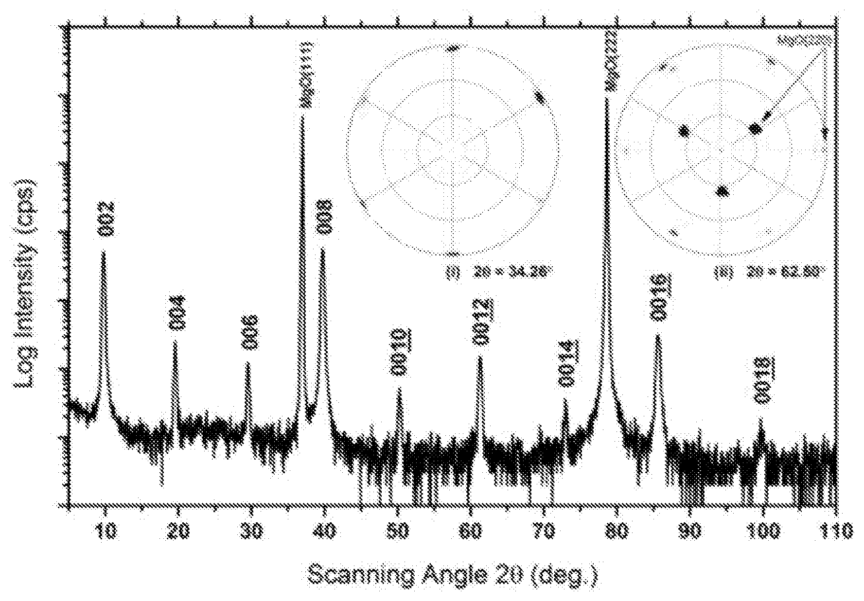
FIG. 1 is an XRD pattern of Mo.sub.2Ga.sub.2C thin film sample. The two peaks with highest intensities at 2.theta.=36.97.degree. and 78.64.degree. are those of the MgO substrate. The other 9 peaks come from the thin film and represent a series of interplanar spacing d with a least common multiple of .about.9.04 .ANG.. The pole figure labelled (i) was acquired at a constant 2.theta.=34.26.degree.--and one labelled (ii) was acquired at 2.theta.=62.50.degree..
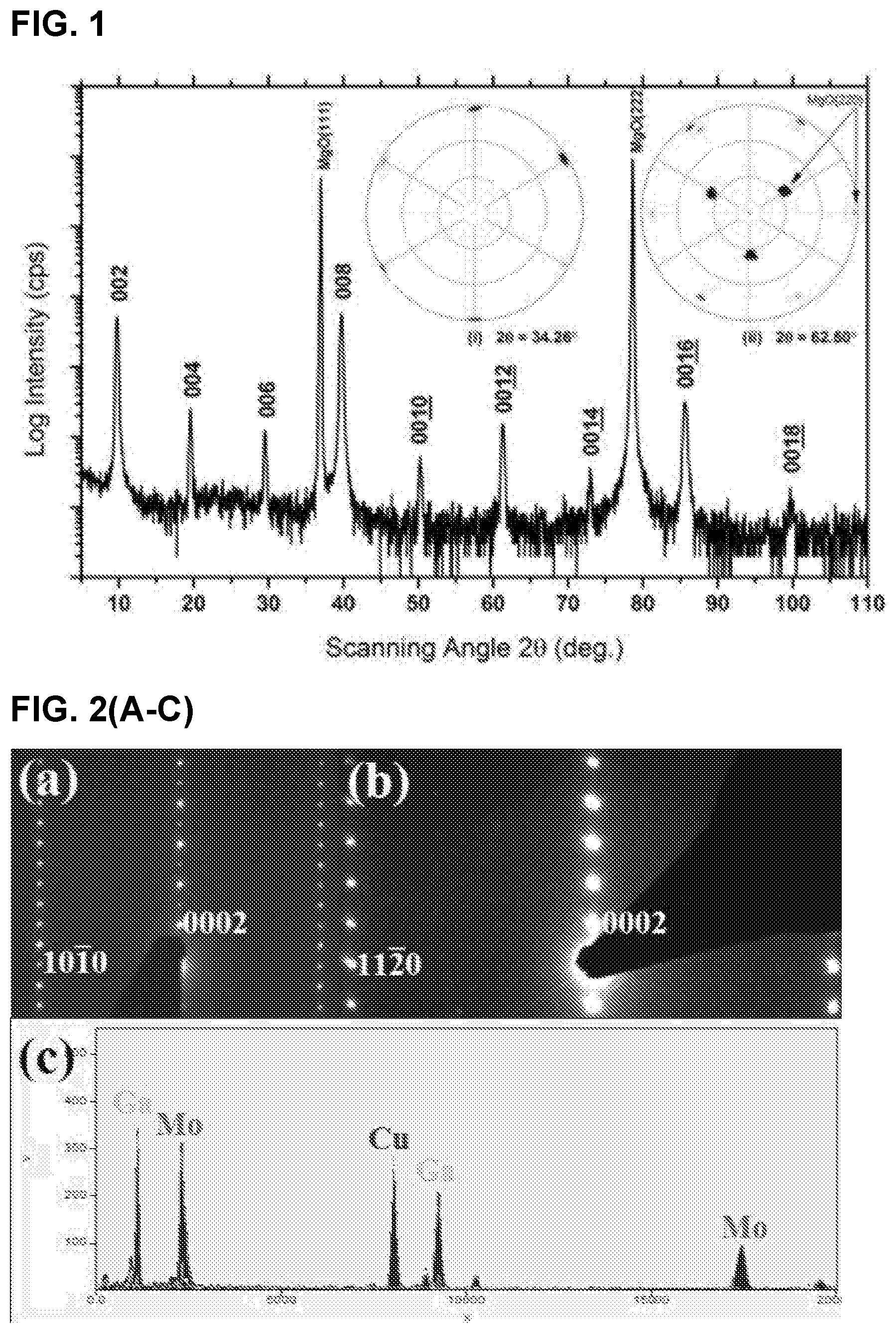
FIG. 2 illustrates (A) Selected area electron diffraction of Mo.sub.2Ga.sub.2C thin films in [1120] and, (B) [1010] zone axes, (C) EDS spectrum; (D) high-angle annular dark field (HAADF) images in the (D) [1120] and, (E) [1010] zone axes. Insets are corresponding atomic structure models of indicating corresponding positions of Ga and Mo atoms in the stacking sequence
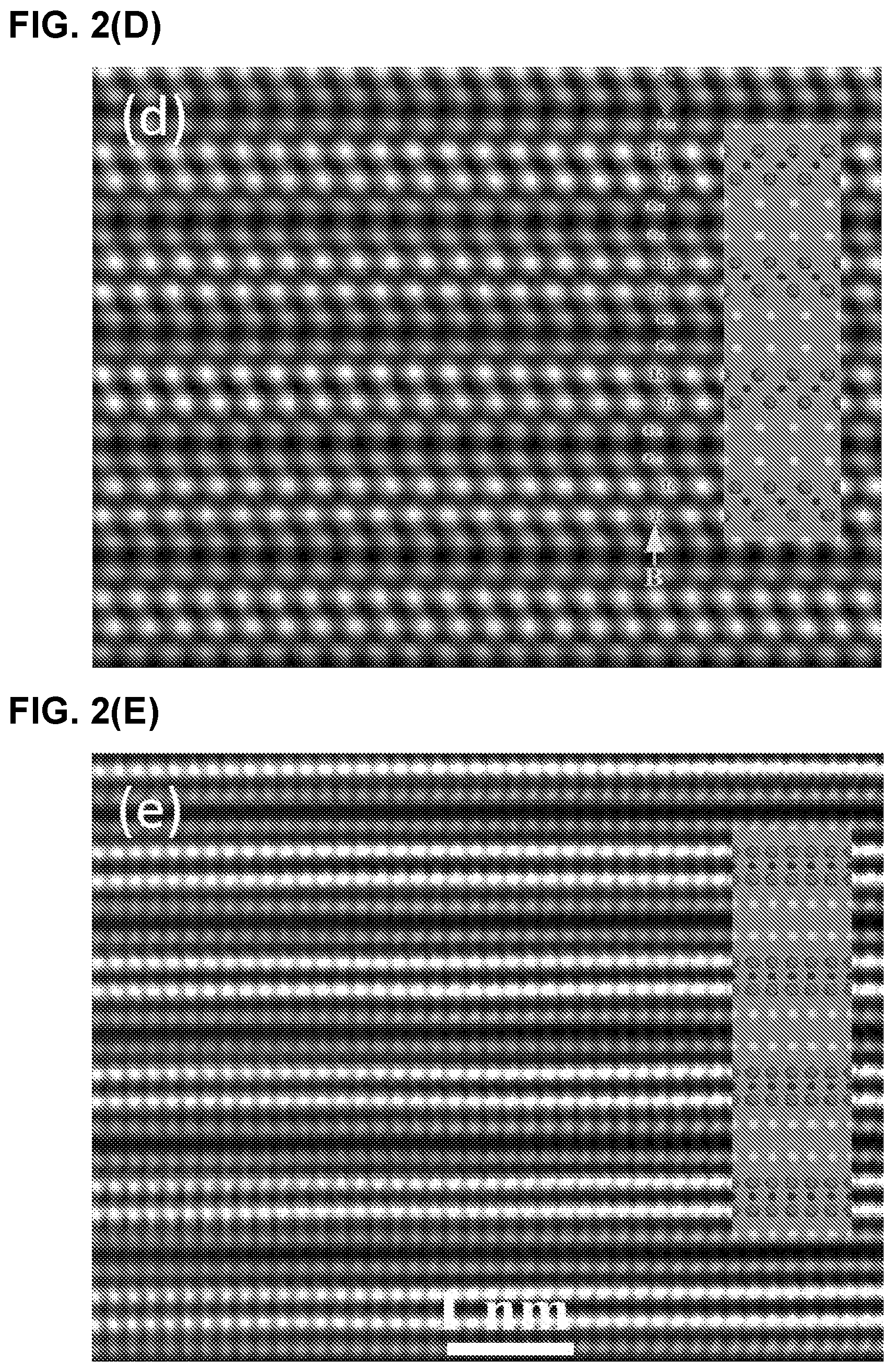
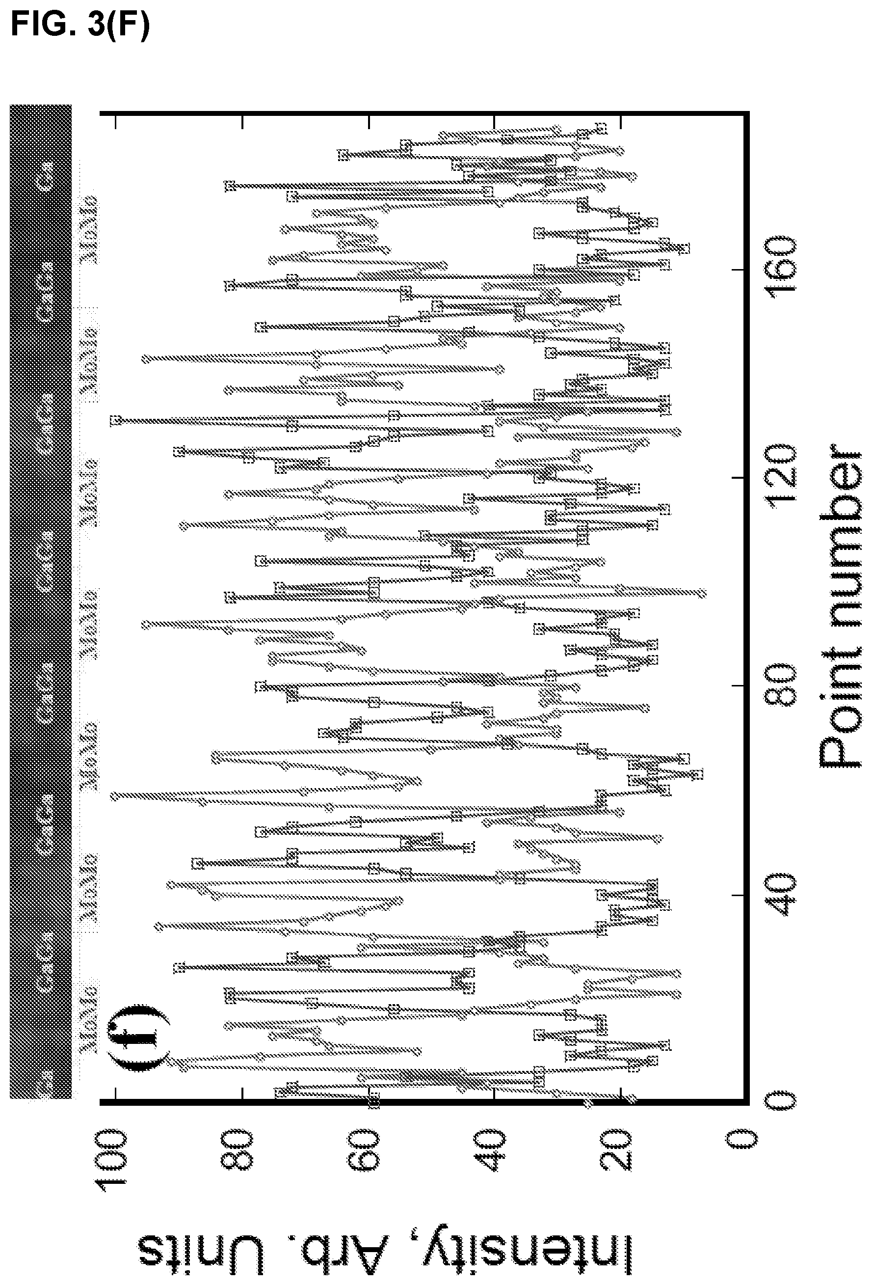
FIG. 3 illustrates (A) HAADF image and corresponding (B), Mo, (C) Ga, and, (D) Mo and Ga maps, (E) HAADF image superimposed with Mo and Ga maps, (F) line scan along [0001] direction a Mo.sub.2Ga.sub.2C film (Ga, square points and Mo, circle points).
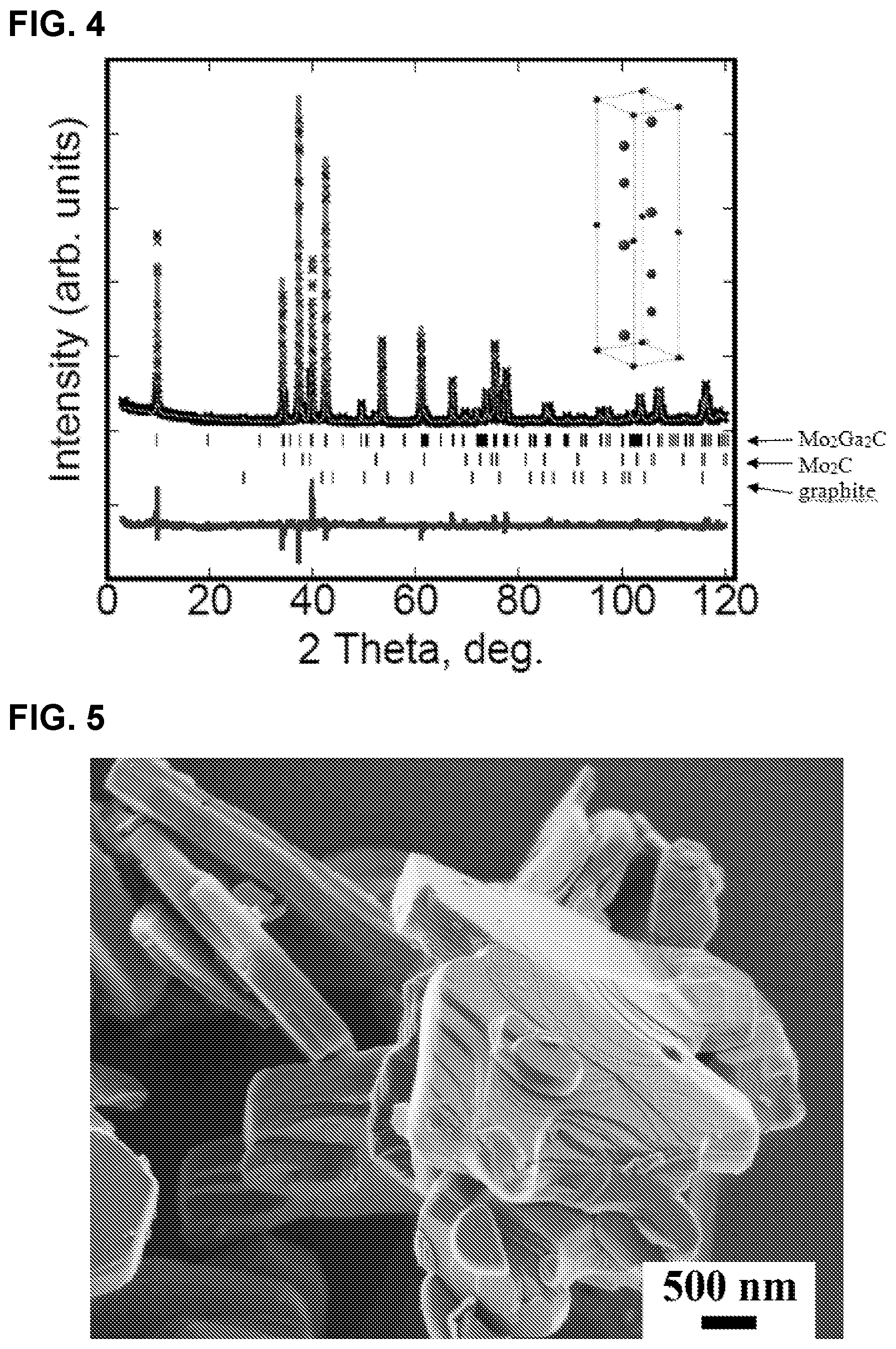
FIG. 4 illustrates are powder XRD patterns indexed to Mo.sub.2Ga.sub.2C showing observed pattern (black crosses), Rietveld generated pattern (red line) and difference between the two (blue line). The ticks below the pattern represent the peak positions of Mo.sub.2Ga.sub.2C phase, Mo.sub.2C phase, and graphite phase, respectively. The .chi.2 value was 3.78. Inset shows schematic of unit cell.
FIG. 5 is a scanning electron microscope micrograph of Mo.sub.2Ga.sub.2C powders showing typical MAX phase platelet morphology
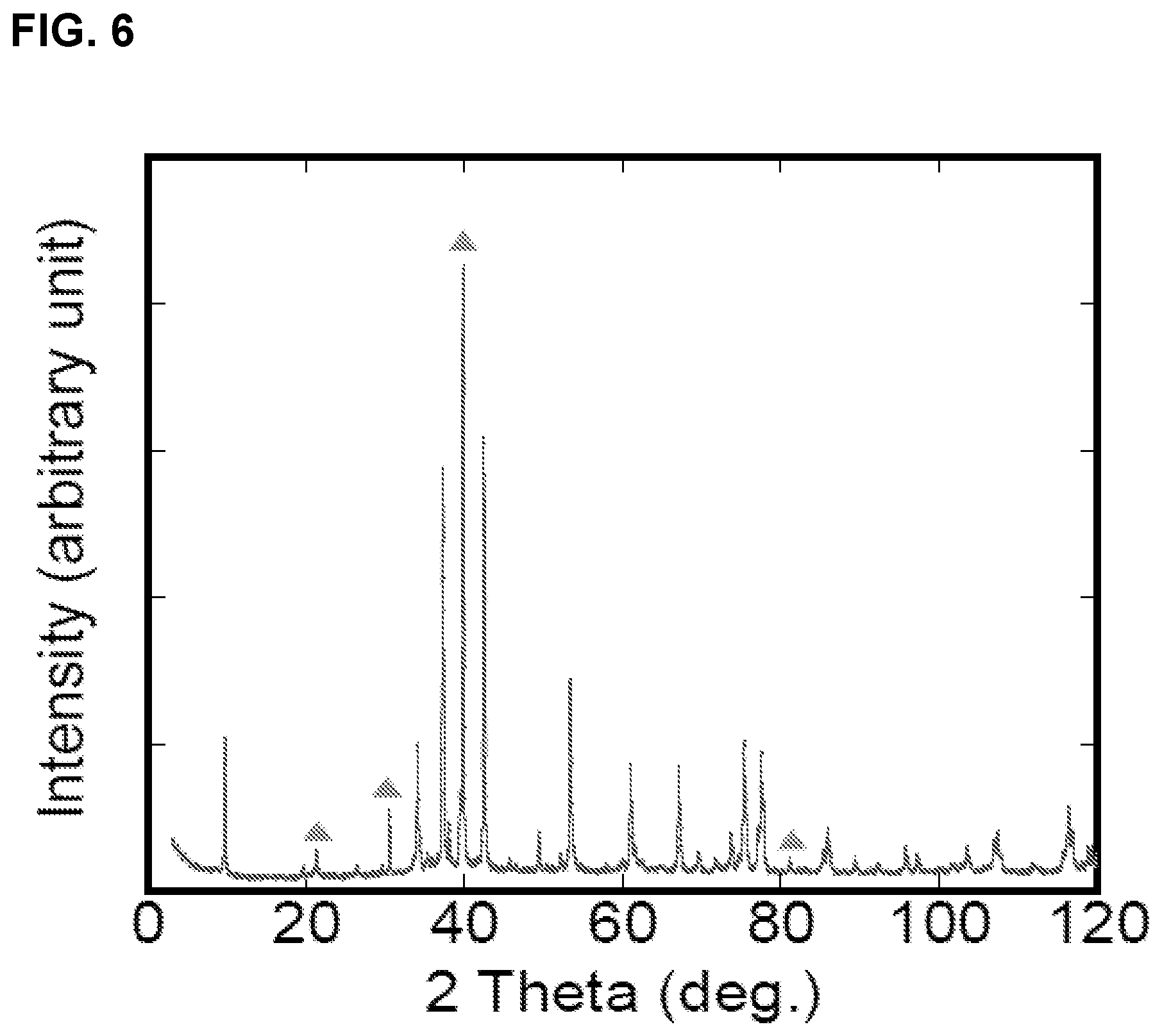
FIG. 6 is an XRD pattern of Mo.sub.2Ga.sub.2C bulk sample, the triangle markers represent peaks for free gallium.
DETAILED DESCRIPTION OF ILLUSTRATIVE EMBODIMENTS
The present invention describes a new class of MAX-phase materials, these having the stoichiometry M.sub.2A.sub.2(C.sub.xN.sub.y), where x+y=1. Mo.sub.2Ga.sub.2C is a particular embodiment within this class
The present invention may be understood more readily by reference to the following detailed description taken in connection with the accompanying Figures and Examples, which form a part of this disclosure. It is to be understood that this invention is not limited to the specific products, methods, conditions or parameters described and/or shown herein, and that the terminology used herein is for the purpose of describing particular embodiments by way of example only and is not intended to be limiting of any claimed invention. Similarly, unless specifically otherwise stated, any description as to a possible mechanism or mode of action or reason for improvement is meant to be illustrative only, and the invention herein is not to be constrained by the correctness or incorrectness of any such suggested mechanism or mode of action or reason for improvement. Throughout this text, it is recognized that the descriptions refer both to compositions and to the articles and devices derived therefrom, as well as the methods of manufacture and use.
In the present disclosure the singular forms "a," "an," and "the" include the plural reference, and reference to a particular numerical value includes at least that particular value, unless the context clearly indicates otherwise. Thus, for example, a reference to "a material" is a reference to at least one of such materials and equivalents thereof known to those skilled in the art, and so forth.
When values are expressed as approximations by use of the antecedent "about," it will be understood that the particular value forms another embodiment. In general, use of the term "about" indicates approximations that can vary depending on the desired properties sought to be obtained by the disclosed subject matter and is to be interpreted in the specific context in which it is used, based on its function, and the person skilled in the art will be able to interpret it as such. In some cases, the number of significant figures used for a particular value may be one non-limiting method of determining the extent of the word "about." In other cases, the gradations used in a series of values may be used to determine the intended range available to the term "about" for each value. Where present, all ranges are inclusive and combinable. That is, reference to values stated in ranges includes each and every value within that range.
It is to be appreciated that certain features of the invention which are, for clarity, described herein in the context of separate embodiments, may also be provided in combination in a single embodiment. That is, unless obviously incompatible or specifically excluded, each individual embodiment is deemed to be combinable with any other embodiment(s) and such a combination is considered to be another embodiment. Conversely, various features of the invention that are, for brevity, described in the context of a single embodiment, may also be provided separately or in any sub-combination. Finally, while an embodiment may be described as part of a series of steps or part of a more general structure, each said step may also be considered an independent embodiment in itself, combinable with others.
The transitional terms "comprising," "consisting essentially of" and "consisting" are intended to connote their generally in accepted meanings in the patent vernacular; that is, (i) "comprising," which is synonymous with "including," "containing," or "characterized by," is inclusive or open-ended and does not exclude additional, unrecited elements or method steps; (ii) "consisting of" excludes any element, step, or ingredient not specified in the claim; and (iii) "consisting essentially of" limits the scope of a claim to the specified materials or steps "and those that do not materially affect the basic and novel characteristic(s)" of the claimed invention. Embodiments described in terms of the phrase "comprising" (or its equivalents), also provide, as embodiments, those which are independently described in terms of "consisting of" and "consisting essentially of" For those embodiments provided in terms of "consisting essentially of" the basic and novel characteristic(s) is the novel structures described herein. For example, the term "consisting essentially of molybenum, gallium, and carbon" refers to a composition containing at least these elements, but the presence of any additional elements is insufficient to compromise the crystalline 2-2-1 structure of the Mo.sub.2Ga.sub.2C MAX phase composition.
When a list is presented, unless stated otherwise, it is to be understood that each individual element of that list, and every combination of that list, is a separate embodiment. For example, a list of embodiments presented as "A, B, or C" is to be interpreted as including the embodiments, "A," "B," "C," "A or B," "A or C," "B or C," or "A, B, or C."
Various embodiments of this invention provide for crystalline solids, each crystalline solid having an empirical formula of M.sub.2A.sub.2X.
wherein M is at least one Group IIIB, IVB, VB, or VIB metal, preferably Cr, Hf, Sc, Ti, Mo, Nb, Ta, V, Zr, or a combination thereof (more preferably Mo);
wherein A is Al, Ga, Ge, In, Pb, or Sn, or a combination thereof (preferably Ga); and
each X is C.sub.xN.sub.y, where x+y=1.
As described herein, the terms "M" or "M atoms," "M elements," or "M metals" refers to one or more members of the Groups IIIB, IVB, VB, or VIB or (aka) Groups 3-6 of the periodic table, either alone or in combination, said members at least including Sc, Y, Lu, Ti, Zr, Hf, V, Nb, Ta, Cr, Mo, and W. The terms "M" or "M atoms," "M elements," or "M metals" may also include Mn. In preferred embodiments, the transition metal is one or more of Sc, Ti, Zr, Hf, V, Nb, Ta, Cr, and/or Mo. In even more preferred embodiments, the transition metal is Mo.
The range of compositions available can be seen as extending even further when one considers that each M-atom position within the overall M.sub.2A.sub.2X matrix can be represented by more than one element. That is, one or more type of M-atom can occupy each M-positions within the respective matrices. In certain exemplary non-limiting examples, these can be (M.sup.A.sub.xM.sup.B.sub.y).sub.2A.sub.2C or (M.sup.A.sub.xM.sup.B.sub.y).sub.2A.sub.2N, where M.sup.A and M.sup.B are independently members of the same chemical group (taken from the specific Group embodiments described elsewhere herein), and x+y=1. In the same way, one or more type of X-atom can occupy each X-position within the matrices, for example solid solutions of the formulae M.sub.2A.sub.2(C.sub.xN.sub.y), or (M.sup.A.sub.xM.sup.B.sub.y).sub.2A.sub.2(C.sub.xN.sub.y), where x and y are independent at each occurrence and x+y=1.
Previously known MAX phase compositions having the general: M.sub.n+1AX.sub.n, (MAX) where n=1 to 3, are generally recognized as comprising layered, hexagonal carbides and nitrides, in which M is typically described as an early transition metal (comprising a Group IIIB, IVB, VB, or VIB metal, or Mn), A is described as an A-group (mostly IIIA and IVA, or groups 13 and 14) element and X is either carbon and/or nitrogen. See, e.g., M. W. Barsoum, et al., "Synthesis and Characterization of a Remarkable Ceramic: Ti.sub.3SiC.sub.2," J. Amer. Ceramics. Soc., 79, 1953-1956 (1996); M. W. Barsoum, "The M.sub.N+1AX.sub.N Phases: A New Class of Solids: Thermodynamically Stable Nanolaminates,"Progress in Solid State Chemistry, 28, 201-281 (2000), both of which are incorporated by reference herein. While Ti.sub.3AlC.sub.2 is among the most widely studied of these materials, more than 60 MAX phases are currently known to exist and are useful in the present invention.
While the present disclosure describes the specific features of Mo.sub.2Ga.sub.2C, as the exemplary 2-2-1 MAX phase material, it is expected that these 2-2-1 crystalline solids also may include one or more of Cr.sub.2Ga.sub.2C, Cr.sub.2Ga.sub.2N, Mo.sub.2Ga.sub.2N, Nb.sub.2Ga.sub.2C, Nb.sub.2Ga.sub.2N, Ta.sub.2Ga.sub.2C, Ta.sub.2Ga.sub.2N, Ti.sub.2Ga.sub.2C, Ti.sub.2Ga.sub.2N, V.sub.2Ga.sub.2C, or V.sub.2Ga.sub.2N.
In other embodiments of the present invention, these 2-2-1 crystalline solids may include one or more of Hf.sub.2In.sub.2C, Hf.sub.2In.sub.2N, Hf.sub.2Sn.sub.2C, Hf.sub.2Sn.sub.2N, Nb.sub.2In.sub.2C, Nb.sub.2In.sub.2N, Nb.sub.2Sn.sub.2C, Nb.sub.2Sn.sub.2N, Sc.sub.2In.sub.2C, Sc.sub.2In.sub.2N, Ti.sub.2In.sub.2C, Ti.sub.2In.sub.2N, Ti.sub.2Sn.sub.2C, Ti.sub.2Sn.sub.2N, Zr.sub.2In.sub.2C, Zr.sub.2In.sub.2N, Zr.sub.2Sn.sub.2C, or Zr.sub.2Sn.sub.2N.
Again, while the presence of gallium in the Mo.sub.2Ga.sub.2C described herein has been realized in practice, the close size relationship of other M and A element atoms support the inclusion of the other M and A elements in M.sub.2A.sub.2X materials within the scope of the present invention.
TABLE-US-00001 Atomic MAX Phase Radius, pm material? A-Element Aluminum 118 Yes Germanium 125 Yes Astatine 127 Yes Gallium 136 Yes Tin 145 Yes Lead 154 Yes Indium 156 Yes Thallium 156 Yes M-Element Chromium 166 Yes Vanadium 171 Yes Titanium 176 Yes Scandium 184 Yes Molybdenum 190 Yes Niobium 198 Yes Tantalum 200 Yes Zirconium 206 Yes Hafnium 208 Yes
Generally, previously known M.sub.n+1AX.sub.n phase materials are themselves known to exist as laminated structures with anisotropic properties. These materials are layered hexagonal (space group P6.sub.3/mmc), with two formula units per unit cell. Such also appears to be the case with these new 2-2-1 MAX phase materials. Near close-packed M-layers are interleaved with pure A-group element layers, with the X-atoms filling the octahedral sites between the former. In the case of the 2-2-1 materials, the near close packed M-layers are interleaved with two A-group element layers. Accordingly, in certain embodiments, the 2-2-1 materials have structures characterized as comprising two layers of Ga, In, or Sn atoms stacked between the corresponding Cr.sub.2C, Cr.sub.2N, Hf.sub.2C, Hf.sub.2N, Mo.sub.2C, Mo.sub.2N, Nb.sub.2C, Nb.sub.2N, Sc.sub.2C, Sc.sub.2N, Ta.sub.2C, Ta.sub.2N, Ti.sub.2C, Ti.sub.2N, V.sub.2C, V.sub.2N, Zr.sub.2C, or Zr.sub.2N layers or mixed metal layers of TiZrC, TiZrN, TiHfC, TiHfN, ZrHfC, ZrHfN CrMoC, CrMoC, VTaC, VTaN, VNbC, VNbN, TaNbC, or TaNbN. This is demonstrated specifically for Mo.sub.2Ga.sub.2C, where two layers of Ga atoms are stacked between Mo.sub.2C layers, the structure exhibiting a simple hexagonal arrangement.
These 2-2-1 MAX-phase materials can also be characterized by their X-ray diffraction (XRD) spectra (see FIG. 1 and Table 1). For example, certain embodiments provide crystalline solids comprising or consisting essentially of molybdenum, gallium, and carbon exhibiting at least five of the following characteristic X-ray powder diffraction peaks (Cu K.alpha. radiation, expressed in degrees 2.theta.) at approximately 9.8, 19.6, 29.6, 39.9, 50.4, 61.5, 73.2, 86.0, and 100.2. Additional embodiments include solids that further exhibit other additional peaks shown in FIG. 1, preferably in order of decreasing intensities. Other embodiments provide crystalline solids comprising or consisting essentially of molybdenum, gallium, and carbon exhibiting at least five of the following characteristic X-ray powder diffraction peaks (Cu K.alpha. radiation, expressed in degrees 2.theta.) at approximately 9.8, 34.1, 37.3, 42.5, 53.4, 61.0, and 75.4, and optionally other additional peaks shown in Table 1, preferably in order of decreasing intensities.
The following listing of embodiments is intended to complement, rather than displace or supersede, the previous descriptions.
Embodiment 1
A crystalline solid having an empirical formula of M.sub.2A.sub.2X.
wherein M is at least one Group IIIB, IVB, VB, or VIB metal, preferably Cr, Hf, Sc, Ti, Mo, Nb, Ta, V, Zr, or a combination thereof.
wherein A is Al, Ga, Ge, In, Pb, or Sn, or a combination thereof and
each X is C.sub.xN.sub.y, where x+y=1.
Embodiment 2
The crystalline solid of Embodiment 1 that is Cr.sub.2Ga.sub.2C, Cr.sub.2Ga.sub.2N, Mo.sub.2Ga.sub.2C, Nb.sub.2Ga.sub.2C, Ta.sub.2Ga.sub.2C, Ti.sub.2Ga.sub.2C, Ti.sub.2Ga.sub.2N, V.sub.2Ga.sub.2C, or V.sub.2Ga.sub.2N.
Embodiment 3
The crystalline solid of Embodiment 1 that is Hf.sub.2In.sub.2C, Hf.sub.2In.sub.2N, Hf.sub.2Sn.sub.2C, Hf.sub.2Sn.sub.2N, Nb.sub.2In.sub.2C, Nb.sub.2In.sub.2N, Nb.sub.2Sn.sub.2C, Nb.sub.2Sn.sub.2N, Sc.sub.2In.sub.2C, Sc.sub.2In.sub.2N, Ti.sub.2In.sub.2C, Ti.sub.2In.sub.2N, Ti.sub.2Sn.sub.2C, Ti.sub.2Sn.sub.2N, Zr.sub.2In.sub.2C, Zr.sub.2In.sub.2N, Zr.sub.2Sn.sub.2C, or Zr.sub.2Sn.sub.2N.
Embodiment 4
The crystalline solid of any one of Embodiments 1 to 3, wherein the empirical formula is defined by the unit cell stoichiometry of the crystalline solid.
Embodiment 5
The crystalline solid of Embodiment 1, having a unit cell stoichiometry of Mo.sub.2Ga.sub.2C.
Embodiment 6
The crystalline solid of any one of Embodiments 1 to 5, in which two layers of Ga, In, or Sn atoms are stacked between the corresponding Cr.sub.2C, Cr.sub.2N, Hf.sub.2C, Hf.sub.2N, Mo.sub.2C, Mo.sub.2N, Nb.sub.2C, Nb.sub.2N, Sc.sub.2C, Sc.sub.2N, Ta.sub.2C, Ta.sub.2N, Ti.sub.2C, Ti.sub.2N, V.sub.2C, V.sub.2N, Zr.sub.2C, or Zr.sub.2N layers.
Embodiment 7
The crystalline solid of Embodiment 5, in which two layers of Ga atoms are stacked between otherwise adjacent Mo.sub.2C layers.
Embodiment 8
The crystalline solid of any one of Embodiments 1 to 7, wherein the crystalline structure is arranged in a simple hexagonal arrangement.
Embodiment 9
A crystalline solid comprising or consisting essentially of molybdenum, gallium, and carbon exhibiting at least five of the following characteristic X-ray powder diffraction peaks (Cu K.alpha. radiation, expressed in degrees 2.theta.) at approximately 9.8, 19.6, 29.6, 39.9, 50.4, 61.5, 73.2, 86.0, and 100.2 and optionally other additional peaks shown in FIG. 1, preferably in order of decreasing intensities.
Embodiment 10
A crystalline solid comprising or consisting essentially of molybdenum, gallium, and carbon exhibiting at least five of the following characteristic X-ray powder diffraction peaks (Cu K.alpha. radiation, expressed in degrees 2.theta.) at approximately 9.8, 34.1, 37.3, 42.5, 53.4, 61.0, and 75.4 and other additional peaks shown in Table 1, preferably in order of decreasing intensities.
EXAMPLES
The following Examples are provided to illustrate some of the concepts described within this disclosure. While each Example is considered to provide specific individual embodiments of composition, methods of preparation and use, none of the Examples should be considered to limit the more general embodiments described herein.
In the following examples, efforts have been made to ensure accuracy with respect to numbers used (e.g. amounts, temperature, etc.) but some experimental error and deviation should be accounted for. Unless indicated otherwise, temperature is in degrees C., pressure is at or near atmospheric.
Example 1: Experimental Details
In an effort to synthesize Mo.sub.2GaC, an XRD peak around 9.degree. 2.theta. suggested the possible existence of Mo.sub.3GaC.sub.2. However, since the latter is predicted to be highly unstable, further work described herein, led to the present discovery of a new phase: Mo.sub.2Ga.sub.2C, wherein two Ga layers--instead of one in Mo.sub.2GaC and all other MAX phases--are stacked in a simple hexagonal arrangement in between Mo.sub.2C layers.
Example 1.1. Synthesis of the Bulk Mo.sub.2Ga.sub.2C
The starting materials used were commercial Mo (63 NS, Metco Inc., Anderson, S.C.), graphite (Grade 4827, Asbury Graphite Mills Inc., Asbury, N.J.) powders and Ga shots (99.99%) (Roto Metals Inc., San Leandro, Calif.). First the Mo and graphite powders were weighed in a 2:1 molar ratio and placed in a plastic bottle and mixed for 24 h using agate balls as the milling media. This mixture was then mixed with the Ga shot in an agate mortar.
Bulk Mo.sub.2Ga.sub.2C samples were synthesized by, first heating a 2:1 molar ratio of Mo:C powders in flowing Ar at 1000.degree. C. for 12 h. The resulting, lightly sintered, Mo2C compact was crushed into a powder and mixed with Ga in 1:1 molar ratio. This mixture was then sealed under a mechanical vacuum in a 100 mm long quartz tube, and sintered at 850.degree. C. for 24 h. XRD diffraction patterns of the resulting material showed the presence of significant amounts of unreacted Ga. To dissolve the latter, the powders were immersed in 37% HCl for 4 days.
Example 1.2. Alternate Method for Synthesizing Bulk Mo.sub.2Ga.sub.2C
Powders of Mo.sub.2Ga.sub.2C were synthesized by a solid liquid reaction of Mo.sub.2C and Ga. In brief, a -325 mesh Mo.sub.2C powder and Ga (both from Alfa Aesar, Ward Hill, Mass., both of 99.5 wt % purity) were mixed in a 1:8 molar ratio and placed in a quartz tube that was evacuated using a mechanical vacuum pump and sealed. The latter was placed in a horizontal tube furnace that was heated at a rate of 10.degree. C. min.sup.-1 to 850.degree. C., and held at that temperature for 48 h. After furnace cooling, the lightly sintered material was crushed, using a mortar and pestle, and returned back to the quartz tube. The latter was evacuated and re-heated at a rate of 10.degree. C. min.sup.-1 to 850.degree. C. and held at temperature for 16 h more. Rietveld refinement of the XRD patterns for Mo.sub.2Ga.sub.2C indicated that <20 wt % Mo.sub.2C was present in the powders as a secondary phase.
One gram of the lightly sintered Mo.sub.2Ga.sub.2C compact was immersed in a 20 mL of 12 M HCl solution (technical grade, Fisher Scientific, Fair Lawn, N.J.) for 2 d, at RT, while being stirred using a Teflon coated magnet on a stir plate to dissolve any unreacted Ga. The powders were washed with DI water several times (until the pH of the wash water was ca. 6), then dried by filtration using a nanoporous polypropylene membrane.
Example 1.3. Removal of Gallium from Mo.sub.2Ga.sub.2C to Form Mo.sub.2CT.sub.x Flakes--Method 1
One gram of Mo.sub.2Ga.sub.2C powder was added to 20 mL of a premixed solution of 3 M of LiF (90+%, Ward Hill, Mass., Alfa Aesar) and 12 M HCl. The Mo.sub.2Ga.sub.2C containing mixture was placed on a magnetic stirrer hot plate in an oil bath held at 35.degree. C. for various times. Afterwards, the mixture was washed through three cycles of 1 M of aqueous HCl, followed by three cycles of 1 M of aqueous LiCl (Alfa Aesar, 98+%), and finally cycles of DI water until the supernatant reached a pH of approximately 6. In each cycle, the washing was performed by adding 40 mL volume of the solution to the washed powders in a centrifuge tube, and the tube was hand-shaken for 1 min before centrifuging at 5000 rpm for 2 min. 20 mL of argon, Ar, deaerated DI water were then added to the washed powder, which was then hand shaken for 5 min., followed by centrifuging for 1 h at 5000 rpm. The supernatant was collected for further investigation. The settled powder was discarded. The product was characterized to be a MXene composition of Mo.sub.2CT.sub.x (i.e., a 2-D lattice having a unit cell composition of Mo.sub.2C where T.sub.x represents surface terminations of each crystal lattice layer, predominantly by O and OH) intercalated by lithium ions. In this way, the Mo.sub.2Ga.sub.2C responded to this treatment with LiCl and HCl in much the same way as previously observed for extracting aluminum from MAX phase analogs.
Example 1.3. Removal of Gallium from Mo.sub.2Ga.sub.2C to Form Mo.sub.2CT.sub.x Flakes--Method 2
Powders of Mo.sub.2Ga.sub.2C were immersed, slowly, in a bottle containing 14 M aqueous HF (Fisher Scientific, Fair Lawn, N.J.) in a ratio of 1 g to 40 mL. Afterwards the bottle was placed in an oil bath over a stirred hot plate held at 55.degree. C. for 160 h, while stirring using a Teflon coated magnet. The resulting suspension was washed with DI water through several cycles till a pH of ca. 6 was reached. In each cycle, the washing was performed by adding 40 mL of DI water to a centrifuge tube containing the sediment, and then the tube was hand-shaken for 1 min before centrifuging at 5000 rpm for 2 min. The settled powder was removed from the centrifuge tube and filtered through a nanoporous polypropylene membrane (3501 Coated PP, 0.064 micron pore size, Celgard) for further investigation.
One gram of this filtered powder was added to a 10 mL of an aqueous solution of 54-56 wt % tetrabutylammonium hydroxide, (C.sub.4H.sub.9).sub.4NOH, (Sigma Aldrich, St. Louis, Mo.). The mixture was stirred at RT for 18 h. After the prescribed mixing time, the mixture was washed three times by 40 mL deaerated DI water each time and the sediment was used for further characterization and delamination.
Example 1.5. Thin Film Synthesis
Direct current magnetron sputtering was used to grow Mo--Ga--C thin films were synthesized. The films were co-deposited from three elemental targets, Mo (3-inch, 99.95% purity, SCOTECH Ltd.), Ga (2-inch, 99.99999% purity, 5N Plus UK Ltd.) and C (3-inch, 99.99% purity, SCOTECH Ltd.) with respective powers 40 W, 18 W and 200 W and at .about.0.5 Pa Ar with a background pressure in the range of 10-7 Pa. Due to its low melting point (.about.30.degree. C.), the Ga source was kept in a concave stainless steel crucible right below the substrate, in line with previously developed procedures. The Mo and C targets were tilted +35.degree. and -35.degree. away from the horizontal position of the Ga target, co-focusing onto the rotating substrate.
The thin films were grown on MgO (111) substrates (10.times.10.times.0.5 mm.sup.3, Latech Ltd.) that were ultrasonically cleaned sequentially in acetone, ethanol and isopropanol for 10 minutes at each stage. Before deposition, the substrate was heated to 560.degree. C. at the base pressure, followed by a 10 minutes presputtering with the same powers for deposition. A shutter was inserted to blind the substrate from the target's line-of-sight when pre-sputtering, and was afterwards removed directly to start the deposition at the same substrate temperature set-point (560.degree. C.).
Example 2. Characterization Details
Example 2.1. Details of XRD Experimental Parameters and Refinement Conditions
XRD patterns were obtained with a diffractometer (Rikagu Smartlab, Tokyo, Japan), with a step size of 0.02.degree. in the 3.degree.-120.degree. 2 theta range with a step time of 7 s with a 10.times.10 mm.sup.2 window slit. Scans were made with Cu-K.alpha. radiation (40 kV and 44 mA).
Rietveld refinement of the XRD diffractograms was carried out using the FULLPROF code [J. Rodriguez-Carvajal, Phys. B 192 (1993) 55-69]. The refinement was carried out from 8.5.degree. to 120.degree. 2.theta.. Refined parameters were: five background parameters, scale factors from which relative phase fractions are evaluated, Y profile parameter for peak width, lattice parameters (LPs) and atomic positions for all phases. The experimental and those calculated from the Rietveld refinement are summarized in Table 1.
TABLE-US-00002 TABLE 1 X-ray (Cu K.alpha.) powder diffraction data for Mo.sub.2Ga.sub.2C. Peak Num- I calcu- I ob- ber h k l 2theta lated served d-hkl 1 0 0 2 9.778 539.2 595.1 9.038692 2 0 0 4 19.627 12.8 0 4.519346 3 0 0 6 29.626 9 5.4 3.012897 4 1 0 0 34.078 752.1 600 2.628786 5 1 0 1 34.448 111.7 87.2 2.601424 6 1 0 2 35.536 8.9 26.6 2.524197 7 1 0 3 37.289 1745.8 1612.5 2.409481 8 1 0 4 39.631 18.4 17.5 2.272329 9 0 0 8 39.862 661.3 741.6 2.259673 10 1 0 5 42.482 1469.5 1393.4 2.126176 11 1 0 6 45.77 14.5 85.8 1.980804 12 1 0 7 49.433 98.6 103.8 1.842244 13 0 0 10 50.442 7.3 6.8 1.807738 14 1 0 8 53.426 471.5 503.4 1.7136 15 1 0 9 57.715 2 0 1.596029 16 1 1 0 60.999 617.9 522.7 1.51773 17 0 0 12 61.505 13.5 12.9 1.506449 18 1 1 2 61.946 24.7 21.8 1.496776 19 1 0 10 62.281 11.7 9.9 1.489534 20 1 1 4 64.74 4 0 1.438764 21 1 0 11 67.115 230.1 182.8 1.393502 22 1 1 6 69.262 6.6 3.4 1.355463 23 2 0 0 71.754 84 53.4 1.314393 24 2 0 1 71.973 11.2 7.8 1.310932 25 1 0 12 72.22 7.6 7 1.307045 26 2 0 2 72.628 1.7 1.2 1.300712 27 0 0 14 73.247 1.7 1.6 1.291242 28 2 0 3 73.715 228.1 189.5 1.284197 29 2 0 4 75.227 2.2 2 1.262098 30 1 1 8 75.379 586.3 496.7 1.259917 31 2 0 5 77.155 244.3 208.9 1.235294 32 1 0 13 77.61 273.3 286.2 1.229188 33 2 0 6 79.492 3.1 6 1.204741 34 2 0 7 82.232 19.1 8.3 1.171398 35 1 1 10 83.011 12.4 10.1 1.162377 36 1 0 14 83.309 0.8 0.3 1.158976 37 2 0 8 85.372 119.4 93.3 1.136165 38 0 0 16 85.965 68.7 76.4 1.129836 39 2 0 9 88.914 0.3 0 1.099836 40 1 0 15 89.358 25.6 0 1.09552 41 1 1 12 92.183 26.6 30.9 1.069186 42 2 0 10 92.868 4.7 4.7 1.063088 43 1 0 16 95.818 75.3 80.9 1.038023 44 2 0 11 97.256 100.1 98.3 1.026468 45 0 0 18 100.17 3.6 4.2 1.004299 46 2 1 0 101.658 81.1 69.6 0.993588 47 2 1 1 101.871 7.7 6.7 0.99209 48 2 0 12 102.112 3.6 3.8 0.990402 49 2 1 2 102.509 2.6 3.9 0.987638 50 1 0 17 102.779 3.5 5.3 0.985778 51 1 1 14 103.116 8.1 12.3 0.983473 52 2 1 3 103.577 243.4 226.4 0.98035 53 2 1 4 105.081 2.4 4.4 0.970412 54 2 1 5 107.029 287.4 254.9 0.958068 55 2 0 13 107.494 161.1 148.3 0.955211 56 2 1 6 109.439 5.7 17.2 0.943602 57 1 0 18 110.383 3.3 6.7 0.938166 58 2 1 7 112.335 20.7 15.1 0.927322 59 2 0 14 113.494 1.1 0.2 0.921122 60 2 1 8 115.752 180.3 136.6 0.909545 61 1 1 16 116.411 317.9 288.6 0.906289 62 0 0 20 116.908 7.8 7.1 0.903869 63 1 0 19 118.859 74.3 57.1 0.894647 64 2 1 9 119.75 0.2 0.1 0.890583
Example 2.2. TEM, XRD and Structural Characterization
The TEM specimens were prepared by mechanic polishing followed by ion thinning down to electron transparency. High resolution scanning electron microscopy (HRSTEM) and X-ray energy dispersive spectroscopy (EDX) were performed with a double Cs corrected FEI Titan3 60-300 operated at 300 kV, equipped with the Super-X EDX system. Selected area electron diffraction (SAED) characterization was carried out using a FEI Tecnai G2 TF20 UT instrument operated at 200 kV with a point resolution of 0.19 nm. Structural characterization of the thin films was performed through X-ray diffraction (XRD). The system utilized was a Panalytical Empyrean MRD with a Cu K.alpha. source. The measurements performed were symmetric (.theta.-2.theta.) scans obtained by employing a hybrid mirror and a 0.27.degree. parallel plate collimator in the incident and the diffracted beam side, respectively.
Example 3. Discussion
The new phase compositions may be produced in two forms: thin film and bulk. In the case of the presently described Mo.sub.2Ga.sub.2C, the thin films were grown by direct current magnetron sputtering of elemental targets on MgO (111) substrates. Bulk Mo.sub.2Ga.sub.2C samples were synthesized by, first heating a 2:1 molar ratio of Mo:C powders in flowing Ar at 1000.degree. C. for 12 h. The resulting, lightly sintered, Mo.sub.2C compact was crushed into a powder and mixed with Ga in 1:1 molar ratio. This mixture was then sealed under a mechanical vacuum in a 100 mm long quartz tube, and sintered at 850.degree. C. for 24 h. XRD diffraction patterns of the resulting material showed the presence of significant amounts of unreacted Ga. To dissolve the latter, the powders were immersed in 37% HCl for 4 days.
The morphologies of all phases resulting from the bulk form were imaged in a scanning electron microscope (SEM) (Supra 50VP, Carl Zeiss AG, Germany) equipped with an energy dispersive spectroscope (EDS). X-ray diffraction, XRD, patterns of the resulting powders were obtained using a diffractometer (see Examples for details). High resolution scanning electron microscopy (HRSTEM) and X-ray energy dispersive spectroscopy (EDX) were performed with a double Cs corrected FEI Titan3 60-300 operated at 300 kV, equipped with the Super-X EDX system. Selected area electron diffraction (SAED) characterization was carried out using a FEI Tecnai G2 TF20 UT instrument operated at 200 kV with a point resolution of 0.19 nm.
FIG. 1 shows a .theta.-2.theta. XRD pattern of a thin film sample, where the two peaks with highest intensities at 2.theta.=36.97.degree. and 78.64.degree. can be assigned (111) and (222) diffractions, respectively, of the MgO substrate. The other nine peaks originate from phases in the thin film with a d spacing with a least common multiple of .about.9.04 .ANG.. The insets in FIG. 1, shows two XRD pole figures of the thin film sample acquired respectively at constant 2.theta.=34.26.degree. (inset (i) in FIG. 1B) and 62.50.degree. (inset (ii) in FIG. 1. At 2.theta.=34.26.degree., six poles can be seen at .PSI.=87-90.degree. with 60.degree. separations in between, which shows a sixfold symmetry in the in-plane directions with respect to the sample surface. This symmetry can be assigned to a phase from the film with an in-plane d spacing of .about.2.62 .ANG.. At 2.theta.=62.50.degree., three poles can be seen at .PSI.=33-39.degree. with 120.degree. separations in between, while two groups of six poles with 60.degree. separations in between are observed at .PSI.=81.degree. and .PSI.=87-90.degree., respectively. The poles at .PSI.=33-39.degree. and 87-90.degree. are assigned to MgO {220} from the MgO (111) substrate, which has a threefold rotational axis along MgO[111]. The sixfold symmetric poles at .PSI.=81.degree. can be assigned to a phase oriented in accordance with the in-plane orientation of the substrate, i.e. it is epitaxially grown on the MgO substrate.
FIGS. 2(A) and (B) are SAED patterns from the new compound. The phase has a hexagonal structure with a and c lattice parameters of 3.05 .ANG. and 18.19 .ANG., respectively. The possibility that those patterns originate from a 312 MAX structure (i.e., the hypothetical Mo.sub.3GaC.sub.2 which is not stable) can be excluded for the following reasons. As noted above, the chemical composition analysis shown in FIG. 2(C) exhibits a different Mo/Ga ratio from that of Mo.sub.3GaC.sub.2 phase. The structure is also not that of Ta.sub.2S.sub.2C and Nb.sub.2S.sub.2C phases, which have the same or at least similar "221" stoichiometries, since they belong to the space group R-3m. Furthermore the stacking observed in HRSTEM (below), is inconsistent with either of these sulphides or a 312 MAX phase.
To reveal the detailed structure, Z contrast image was carried out by HRSTEM. FIG. 2(C) and FIG. 2(D) show HRSTEM images with the beam aligned along the [1120] and [1010] zone axes, respectively. The Z contrast images show a double-layer structural feature. The bright and dark spots should correspond to the Mo and Ga atoms, respectively.
The corresponding EDX maps shown in FIG. 3(A-F) confirm the Mo--Mo--Ga--Ga--Mo--Mo layering. The simplest description of the structure is the following: Start with a 211 MAX phase structure and simply insert one extra Ga layer on top of the existing Ga. Surprisingly, the two Ga layer lie exactly on top of each other (i.e. not close-packed), an unusual arrangement indeed. Indeed this stacking structure is further supported by the facile way in which Mo.sub.2Ga.sub.2C is convertible to Mo.sub.2C MXene with the removal of Ga. See Examples 1.3 and 1.4.
Based on the Z-contrast images, the distance between adjacent Mo layers was estimated to be 2.27 .ANG.. The separation width between the Mo and Ga layers is shortest: 2.09 .ANG.. The same stacking position of the two adjacent Ga layers leads a large separation width. The separation width between the adjacent Ga layers is about 2.64 .ANG.. Based on the measured data, initial atomic positions of Mo and Ga are found and used as input data to the Rietveld refinement below.
FIG. 4 shows a typical XRD pattern of the phase obtained after dissolving the unreacted Ga from the bulk sample. When this new phase was imaged in a HRSTEM (see above) its structure was found to be unlike any other MAX phase known in that there were two Ga layers separating the Mo.sub.2C blocks. Making use of this insight, the XRD pattern was analyzed assuming the unit cell shown in inset of FIG. 4.
To determine the composition of this new phase elastic recoil detection analysis (ERDA) was carried out on a close to phase pure thin film sample containing traces of Mo--C intermetallic phases, and the Mo, Ga and C contents, in at. %, were found to be, respectively, 38.9%, 42.5%, 18.3%, with a trace amount of oxygen. (0.34 at. %). The composition is consistent with 2:2:1 within the error margins of the technique.
The results of Rietveld analysis are summarized in Table 2. The space group assumed was that of the MAX phases: P63/mmc. The a and c-lattice parameters were calculated to be 3.03662(4) .ANG. and 18.0855(3) .ANG., respectively. In addition to the Mo.sub.2Ga.sub.2C phase, the Rietveld refinements indicated the presence of 7.35(0.16) wt. % Mo.sub.2C and 5.22(0.92) wt. % graphite. When these phases were taken into account, the .chi.2 value was 3.78. The occupancies were fixed to be 100% for Mo, Ga and C.
A list of the hkl indices of the various peaks--theoretical and experimentally observed--and their intensities and d spacings are listed in Table 1, which shows generally good agreement between theory and experiment. It should be noted here that since the simple hexagonal arrangement of the Ga atoms is somewhat unusual, other arrangements were tested, where the Ga layers were sheared with respect to each other. The .chi.2 values in those cases were significantly higher than for the unit cell shown in inset of FIG. 1(A).
TABLE-US-00003 TABLE 2 Atomic positions in Mo.sub.2Ga.sub.2C determined from Rietveld analysis of XRD pattern shown in FIG. 1. The space group was P63/ mmc. The a and c-lattice parameters were calculated to be 3.03662(4) .ANG. and 18.0855(3) .ANG., respectively. Wykcoff Element x y z positions Mo 1/3 2/3 0.06434 (10) 4f Ga 1/3 2/3 0.68238 (10) 4f C 0 0 0 2a
The following references may be useful in understanding some elements of the present invention or background principles thereof 1. M. W. Barsoum, MAX Phases: Properties of Machinable Carbides and Nitrides, Wiley VCH GmbH & Co., Weinheim, 2013. 2. P. Eklund, M. Beckers, U. Jansson, H. Hogberg and L. Hultman, Thin Solid Films, 2010, 518 1851-1878. 3. Z.-M. Sun, International Materials Reviews, 2011, 56, 143-166. 4. L. Toth, J. Less Comm. Met., 1967, 13 129.about.131. 6. I. R. Shein and A. L. Ivanovskii, Physica C, 2010, 470, 533-537. 7. R. P. Ziebarth, J. K. Vassiliou and F. J. Disalvo, J. Less Comm. Met., 1989, 156, 207-211. 8. O. Beckmann, H. Boller and H. Nowotny, Monatsh. Chem., 1970, 101, 945 955. 9. H. Kudielka and H. Rohde, Z. Kristalogr., 1960, 114, 447. 10. H. Nowotny, Prog. Solid State Chem., 1970, 2, 27-70. 11. M. W. Barsoum, L. Farber, I. Levin, A. Procopio, T. El-Raghy and A. Berner, J. Amer. Cer. Soc., 1999, 82, 2545-2547. 12. A. Petruhins, A. S. Ingason, M. Dahlqvist, A. Mockute, M. Junaid, J. Birch, J. Lu, L. Hultman, P. O. .ANG.. Persson and J. Rosen, Phys. Status Solidi RRL, vol. 7, no. 11, pp. 971-974, 2013.
It is to be understood that while the invention has been described in conjunction with the preferred specific embodiments thereof, that the foregoing description and the examples that follow are intended to illustrate and not limit the scope of the invention. It will be understood by those skilled in the art that various changes may be made and equivalents may be substituted without departing from the scope of the invention, and further that other aspects, advantages and modifications will be apparent to those skilled in the art to which the invention pertains. In addition to the embodiments described herein, the present invention contemplates and claims those inventions resulting from the combination of features of the invention cited herein and those of the cited prior art references which complement the features of the present invention. Similarly, it will be appreciated that any described material, feature, or article may be used in combination with any other material, feature, or article, and such combinations are considered within the scope of this invention.
The disclosures of each patent, patent application, and publication cited or described in this document are hereby incorporated herein by reference, each in its entirety, for all purposes.
* * * * *
References
D00000
D00001
D00002
D00003
D00004
D00005
D00006
XML
uspto.report is an independent third-party trademark research tool that is not affiliated, endorsed, or sponsored by the United States Patent and Trademark Office (USPTO) or any other governmental organization. The information provided by uspto.report is based on publicly available data at the time of writing and is intended for informational purposes only.
While we strive to provide accurate and up-to-date information, we do not guarantee the accuracy, completeness, reliability, or suitability of the information displayed on this site. The use of this site is at your own risk. Any reliance you place on such information is therefore strictly at your own risk.
All official trademark data, including owner information, should be verified by visiting the official USPTO website at www.uspto.gov. This site is not intended to replace professional legal advice and should not be used as a substitute for consulting with a legal professional who is knowledgeable about trademark law.