High reliable OTP memory with low reading voltage
Liao , et al. Dec
U.S. patent number 10,510,427 [Application Number 16/075,980] was granted by the patent office on 2019-12-17 for high reliable otp memory with low reading voltage. This patent grant is currently assigned to SICHUAN KILOWAY ELECTRONICS INC.. The grantee listed for this patent is SICHUAN KILOWAY ELECTRONICS INC.. Invention is credited to Xuyang Liao, Junhua Mao, Jack Z. Peng.


| United States Patent | 10,510,427 |
| Liao , et al. | December 17, 2019 |
High reliable OTP memory with low reading voltage
Abstract
The present invention relates to the technical field of integrated circuits. Disclosed is a one-time programmable memory with a high reliability and a low reading voltage, comprising: a first MOS transistor, a second MOS transistor, and an antifuse component. A gate terminal of the first MOS transistor is connected to a second connecting line (WS), a first connection terminal of the first MOS transistor is connected to the antifuse component, the antifuse component is connected to a first connecting line (WP), and a second connection terminal of the first MOS transistor is connected to a third connecting line (BL). A first connection terminal of the second MOS transistor is connected to a fourth connecting line (BR), and a second connection terminal of the second MOS transistor is connected to a third connecting line (BL). The invention further comprises a voltage limiting device with a control terminal and two connection terminals.
| Inventors: | Liao; Xuyang (Chengdu, CN), Mao; Junhua (Chengdu, CN), Peng; Jack Z. (Chengdu, CN) | ||||||||||
|---|---|---|---|---|---|---|---|---|---|---|---|
| Applicant: |
|
||||||||||
| Assignee: | SICHUAN KILOWAY ELECTRONICS
INC. (Mianyang, CN) |
||||||||||
| Family ID: | 57099778 | ||||||||||
| Appl. No.: | 16/075,980 | ||||||||||
| Filed: | February 18, 2016 | ||||||||||
| PCT Filed: | February 18, 2016 | ||||||||||
| PCT No.: | PCT/CN2016/074007 | ||||||||||
| 371(c)(1),(2),(4) Date: | August 06, 2018 | ||||||||||
| PCT Pub. No.: | WO2017/133026 | ||||||||||
| PCT Pub. Date: | August 10, 2017 |
Prior Publication Data
| Document Identifier | Publication Date | |
|---|---|---|
| US 20190341119 A1 | Nov 7, 2019 | |
Foreign Application Priority Data
| Feb 5, 2016 [CN] | 2016 1 0084553 | |||
| Current U.S. Class: | 1/1 |
| Current CPC Class: | G11C 17/16 (20130101); G11C 17/18 (20130101); H01L 23/5252 (20130101); G11C 8/14 (20130101); G11C 7/18 (20130101); G11C 17/165 (20130101); G11C 5/025 (20130101); H01L 27/11206 (20130101); G11C 5/02 (20130101) |
| Current International Class: | G11C 17/16 (20060101); G11C 17/18 (20060101); G11C 5/02 (20060101); G11C 5/06 (20060101); H01L 23/525 (20060101); H01L 27/112 (20060101) |
| Field of Search: | ;365/96,51 |
References Cited [Referenced By]
U.S. Patent Documents
| 2008/0117660 | May 2008 | Xu |
| 2012/0163072 | June 2012 | Lu |
| 2013/0063999 | March 2013 | Agam |
| 2014/0218110 | August 2014 | Wu |
| 2014/0225178 | August 2014 | Agam |
| 102646450 | Aug 2012 | CN | |||
| 103119657 | May 2013 | CN | |||
| 103219046 | Jul 2013 | CN | |||
| 203325475 | Dec 2013 | CN | |||
| 106024064 | Oct 2016 | CN | |||
| 2004199824 | Jul 2004 | JP | |||
Attorney, Agent or Firm: Bayramoglu; Gokalp
Claims
What is claimed is:
1. A high reliable, low reading voltage OTP memory, comprising: a first MOS transistor, a second MOS transistor and an anti-fuse element; wherein a gate of the first MOS transistor is connected to a second line WS, a first end of the first MOS transistor is connected to a first line WP across through the anti-fuse element, and a second end of the first MOS transistor is connected to a third line BL; a first end of the second MOS transistor is connected to a fourth line BR, a second end of the second MOS transistor is connected to the third line BL; the high reliable, low reading voltage OTP memory further comprises a voltage-limit device having one control end and two connection ends; the control end of the voltage-limit device is connected to a control line WB, a first connection end of the voltage-limit device is connected to the anti-fuse element and the first end of the first MOS transistor, and a second connection end of the voltage-limit device is connected to a gate of the second MOS transistor.
2. The high reliable, low reading voltage OTP memory of claim 1, wherein the voltage-limit device is a third MOS transistor.
3. The high reliable, low reading voltage OTP memory of claim 2, wherein the first end of the first MOS transistor is a first drain, and the second end of the first MOS transistor is a first source, the first end of the second MOS transistor is a second drain, and the second end of the second MOS transistor is a second source, a first end of the third MOS transistor is a third drain, and a second end of the third MOS transistor is a third source.
4. The high reliable, low reading voltage OTP memory of claim 2, wherein all of the first MOS transistor, the second MOS transistor and the third MOS transistor are N-type transistors (NMOS) or P-type transistors (PMOS).
5. The high reliable, low reading voltage OTP memory of claim 2, wherein all of the first MOS transistor, the second MOS transistor and the third MOS transistor are symmetrical MOS transistors.
Description
CROSS REFERENCE TO RELATED APPLICATION
This application is the national phase entry of International Application PCT/CN2016/074007, filed on Feb. 18, 2016, which is based upon and claims priority to Chinese Patent Application No. 201610084553.9, filed on Feb. 5, 2016, the entire contents of which are incorporated herein by reference.
TECHNICAL FIELD
The present disclosure is directed to the integrated circuits technology. More particularly, the present disclosure is directed to the field of non-volatile memory cells, applied as the high reliable one-time programmable (OTP) memory cells and array with low reading voltage and low power consumption, which is the kernel element in the high frequency and ultra high frequency RFID (Radio Frequency Identification).
BACKGROUND
The Chinese Patent No. 201080067067.7 discloses a low voltage, low power memory. The memory cell shows in the FIG. 1, and the memory array in the FIG. 2.
For the Prior art memory array in FIG. 2, the voltages for programming and reading of cell A are listed in the Table I.
TABLE-US-00001 TABLE 1 Cell V (WP) V (WS) V (BL) V (BR) Programming A SW/SB 5.5 V 2.5 V 0 V Floating B SW/UB 5.5 V 2.5 V 2.5 V Floating C UW/SB 2.5 V 0 V 0 V Floating D UW/UB 2.5 V 0 V 2.5 V Floating Read A SW/SB 1.0 V 0 V 0 V V Sensing B SW/UB 1.0 V 0 V Floating Floating C UW/SB 0 V 0 V 0 V V Sensing D UW/UB 0 V 0 V Floating Floating SW: Selected Word line, SB: Selected Bit line, UW: Unselected Word line, UB: Unselected Bit line,
As an example, if the Cell B with Row m and Column t has been programmed, and the sequent programming is for the Cell A of Row m and Column s. During the programming of Cell A, the high voltage of Vpp on the WPm causes a high voltage about (Vpp-Vt) at the Grate gmt. Vt is a small voltage difference on the anti-fuse element Cmt of programmed Cell B. The high voltage at the Grate gmt may cause same damage and leakage of the MOS transistor NMt of Cell B, and the reading of Cell B through Sense Amplifier may have some problem.
The above analysis shows the obvious shortage of the prior art.
Since cell B has been programmed, the anti-fuse element is in the condition of conducting.
During the programming of Cell A, the second MOS transistor of Cell B has the operation condition that the gate voltage about 5.5V (i.e. 5.2V), the source voltage and the gain voltage are 2.5V. Therefore, the voltage about 3V is on the gate oxide layer of the second MOS transistor. The damage and degeneration will increase for such MOS transistor, which normally works at the operation voltage of 1.8V or even less.
There is a need in the art for an OTP cell that can achieve improved performance and remedy the deficiencies in the prior art by limiting of the gate voltage of the second MOS transistor.
SUMMARY
This invent discloses an improved OTP cells to solve the problem of high voltage struck in the prior art OTP cells.
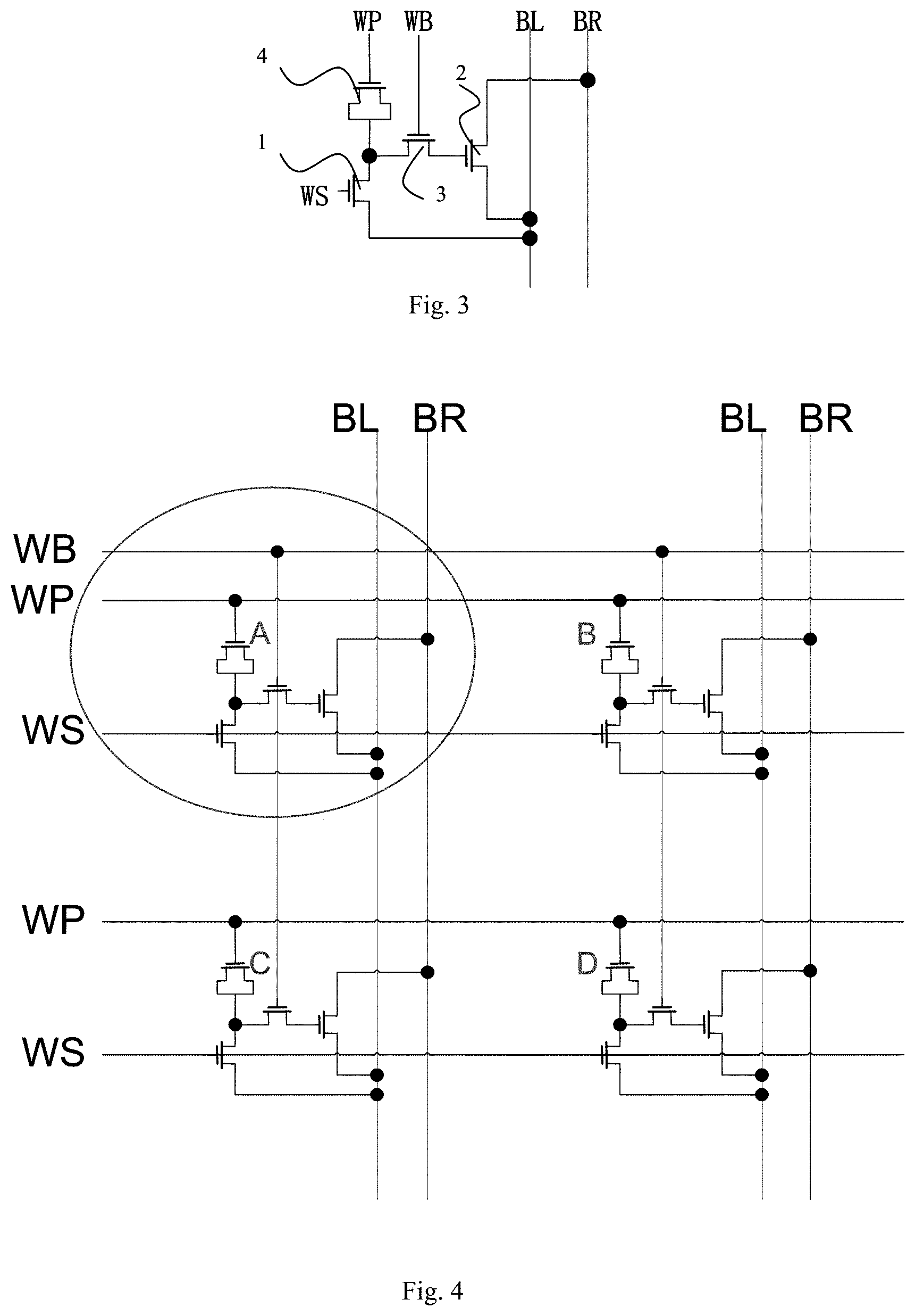
FIG. 3 shows the technical scheme of this invent. The new structure of high reliable, low reading voltage OTP memory cell comprises the first MOS transistor (1), the second MOS transistor (2) and the anti-fuse element (4).
The gate of the first MOS transistor is connected to the second line WS, the first end of the first MOS transistor is connected to the first line WP across through the anti-fuse element, and the second end of the first MOS transistor is connected to the third line BL.
The first end of the second MOS transistor is connected to the fourth line BR, the second end is connected to the third line BL.
In the new structure of FIG. 3, there is a voltage-limit device (3), which has one control end and two connection ends. The control end of the voltage-limit device is connected to the control line WB. One of the connection end of device (3) is connected to the anti-fuse element and the end of the first MOS transistor. The other connection end of device (3) is connected to the gate of the second MOS transistor.
The voltage-limit device is the third MOS transistor (3).
The first end of the first MOS transistor is the drain, and the second end is the source.
The first end of the second MOS transistor is the drain, and the second end is the source.
The first end of the third MOS transistor is the drain, and the second end is the source.
All of the first MOS transistor, the second MOS transistor and the third MOS transistor are N-type transistors (NMOS). In the other embodiment, all of them are P-type transistors (PMOS).
All of the first MOS transistor, the second MOS transistor and the third MOS transistor are symmetrical.
This invent solves the problem of the damage and degeneration of devices in the prior art technologies. For the gate of MOS 2, there is no damage, degeneration or leakage caused by the struck of high voltage. The reliability is improved.
BRIEF DESCRIPTION OF THE DRAWINGS
FIG. 1 shows a prior art memory cell;
FIG. 2 shows a number of prior art memory cells in the cell array architecture;
FIG. 3 shows a memory cell of EMBODIMENT 1, according to the present disclosure
FIG. 4 shows memory cells of FIG. 3 in the cell array architecture;
FIG. 5 shows the memory cells in the cell array architecture for EMBODIMENT 2, according to the present disclosure.
DETAILED DESCRIPTION OF THE EMBODIMENTS
EMBODIMENT 1 is shown in FIG. 3.
The high reliable, low reading voltage OTP memory cell comprises the first MOS transistor (1), the second MOS transistor (2) and the anti-fuse element (4).
The gate of the first MOS transistor is connected to the second line WS, the first end of the first MOS transistor is connected to the first line WP across through the anti-fuse element, and the second end of the first MOS transistor is connected to the third line BL.
The first end of the second MOS transistor is connected to the fourth line BR, the second end is connected to the third line BL.
In the new structure of FIG. 3, there is a voltage-limit device (3), which has one control end and two connection ends. The control end of the voltage-limit device is connected to the control line WB. One of the connection end of device (3) is connected to the anti-fuse element (4) and one end of the first MOS transistor, And the other connection end of device (3) is connected to the gate of the second MOS transistor.
The voltage-limit device is the third MOS transistor (3).
The first end of the first MOS transistor is the drain, and the second end is the source.
The first end of the second MOS transistor is the drain, and the second end is the source.
The first end of the third MOS transistor is the drain, and the second end is the source.
All of the first MOS transistor, the second MOS transistor and the third MOS transistor are N-type transistors (NMOS). In the other embodiment, all of them are P-type transistors (PMOS).
All of the MOS transistors of this embodiment are symmetrical. The drain and the source are mutual exchangeable, so that the connection end of the MOS transistor can be either source or drain. The control end of the MOS transistor is the gate.
The third MOS transistor is in the status of "ON", and an appropriate voltage at the gate can limit the gate voltage of the second MOS transistor.
The structure of memory array shown in FIG. 4 consists in the EMBODIMENT 1 of FIG. 3.
For the memory array of FIG. 4, the voltages for programming and reading of cell A are listed in the Table II.
TABLE-US-00002 TABLE II Cell V(WP) V(WS) V(WB) V(BL) V(BR) Programming A SW/SB 5.5 V 2.5 V 2.5 V 0 V Floating B SW/UB 5.5 V 2.5 V 2.5 V 2.5 V Floating C UW/SB 2.5 V 0 V 2.5 V 0 V Floating D UW/UB 2.5 V 0 V 2.5 V 2.5 V Floating Read A SW/SB 1.0 V Pulse, 0 V 1 V 0 V V Sensing B SW/UB 1.0 V Pulse, 0 V 1 V V, Floating 0 V, Floating C UW/SB 0 V 0 V 1 V 0 V V Sensing D UW/UB 0 V 0 V 1 V V, Floating 0 V, Floating
As listed in Table II, since Cell B has been programmed, during the programming of Cell A, the third MOS transistor of Cell B is used for protecting of the second MOS transistor of Cell B. In more details, if Cell B has been programmed, the anti-fuse element of Cell B is in the "conductive" status. During the programming of Cell A, the ends of the second MOS transistor in Cell B have the voltage status that 2V of gate, 2.5V of both source and drain, respectively. Comparing to the voltages of prior art, such as 5.2V stated in the section of "BACKGROUND", the voltage compression at the gate oxide layer of the second MOS transistor of Cell B reduced significantly. The gate oxide of the second MOS of Cell B is not affected by the high voltage of programming of Cell A.
EMBODIMENT 2 is shown in FIG. 5.
The difference from EMBODIMENT 1 is that EMBODIMENT 2 consists of PMOS transistors. For the programming and read of Cell A, the voltages in the array of FIG. 5. are listed in Table III.
TABLE-US-00003 TABLE III Cell V(WP) V(WS) V(WB) V(BL) V(BR) Programming A SW/SB -5.5 V -2.5 V -2.5 V 0 V Floating B SW/UB -5.5 V -2.5 V -2.5 V -2.5 V Floating C UW/SB -2.5 V 0 V -2.5 V 0 V Floating D UW/UB -2.5 V 0 V -2.5 V -2.5 V Floating Read A SW/SB 1 V 1 V, Pulse 0 V 0 V V Sencing B SW/UB 1 V 1 V, Pulse 0 V Floating 0 V, Floating C UW/SB 0 V 1 V, Pulse 0 V 0 V V Sencing D UW/UB 0 V 1 V, Pulse 0 V Floating 0 V, Floating
* * * * *
D00000
D00001
D00002
D00003
XML
uspto.report is an independent third-party trademark research tool that is not affiliated, endorsed, or sponsored by the United States Patent and Trademark Office (USPTO) or any other governmental organization. The information provided by uspto.report is based on publicly available data at the time of writing and is intended for informational purposes only.
While we strive to provide accurate and up-to-date information, we do not guarantee the accuracy, completeness, reliability, or suitability of the information displayed on this site. The use of this site is at your own risk. Any reliance you place on such information is therefore strictly at your own risk.
All official trademark data, including owner information, should be verified by visiting the official USPTO website at www.uspto.gov. This site is not intended to replace professional legal advice and should not be used as a substitute for consulting with a legal professional who is knowledgeable about trademark law.