Electrical device with flexible connectors
Shepard , et al. Dec
U.S. patent number 10,504,643 [Application Number 15/379,631] was granted by the patent office on 2019-12-10 for electrical device with flexible connectors. This patent grant is currently assigned to HAMILTON SUNSTRAND CORPORATION. The grantee listed for this patent is Hamilton Sundstrand Corporation. Invention is credited to Shin Katsumata, Charles Patrick Shepard.


| United States Patent | 10,504,643 |
| Shepard , et al. | December 10, 2019 |
Electrical device with flexible connectors
Abstract
An electrical device includes a first flexible connector, including a first flexible conductor and a second flexible conductor, and a flexible insulator disposed between the first flexible conductor and the second flexible conductor, a second flexible connector spaced apart from the first flexible connector, the second flexible connector including a third flexible conductor, a first interconnect to electrically connect the first flexible conductor and the third flexible conductor, a second interconnect to electrically connect the third flexible conductor and the second flexible conductor, wherein the second interconnect is disposed opposite the first interconnect.
| Inventors: | Shepard; Charles Patrick (DeKalb, IL), Katsumata; Shin (Rockford, IL) | ||||||||||
|---|---|---|---|---|---|---|---|---|---|---|---|
| Applicant: |
|
||||||||||
| Assignee: | HAMILTON SUNSTRAND CORPORATION
(Charlotte, NC) |
||||||||||
| Family ID: | 60673702 | ||||||||||
| Appl. No.: | 15/379,631 | ||||||||||
| Filed: | December 15, 2016 |
Prior Publication Data
| Document Identifier | Publication Date | |
|---|---|---|
| US 20180174728 A1 | Jun 21, 2018 | |
| Current U.S. Class: | 1/1 |
| Current CPC Class: | H01F 17/062 (20130101); H01F 27/29 (20130101); H01F 27/2895 (20130101); H01F 27/2804 (20130101); H01F 27/292 (20130101); H01F 2027/2814 (20130101); H01F 27/2866 (20130101) |
| Current International Class: | H01F 17/06 (20060101); H01F 27/29 (20060101); H01F 27/28 (20060101) |
| Field of Search: | ;336/200,229,232 |
References Cited [Referenced By]
U.S. Patent Documents
| 5392020 | February 1995 | Chang |
| 5828283 | October 1998 | Choi |
| 7109838 | September 2006 | Brennan |
| 7973635 | July 2011 | Baarman et al. |
| 8538553 | September 2013 | Zhao et al. |
| 9123461 | September 2015 | Carsten |
| 9338895 | May 2016 | Clayton et al. |
| 2003/0025585 | February 2003 | Macerini |
| 2006/0109071 | May 2006 | Thongsouk |
| 2012/0194314 | August 2012 | Mo |
| 2015/0061817 | March 2015 | Lee |
| 2015/0302975 | October 2015 | Qi |
| 4100963 | Jul 1992 | DE | |||
| 1218681 | Jan 1971 | GB | |||
| 2308924 | Feb 2000 | GB | |||
| 61237407 | Oct 1986 | JP | |||
| S61237407 | Oct 1986 | JP | |||
| 1997024739 | Jul 1997 | WO | |||
Other References
|
Search Report dated May 14, 2018 in U380837EP, EP Application No. 17207726, 9 pages. cited by applicant. |
Primary Examiner: Chan; Tszfung J
Attorney, Agent or Firm: Cantor Colburn LLP
Claims
What is claimed is:
1. An electrical device, comprising: a continuous ring-shaped first flexible connector defining an annular space, the continuous ring-shaped first flexible connector including: a first flexible conductor and a second flexible conductor; and a flexible insulator disposed between the first flexible conductor and the second flexible conductor; a continuous ring-shaped second flexible connector disposed within the annular space and spaced apart from the continuous ring-shaped first flexible connector to define a ring-shaped annular region between an interior of the continuous ring-shaped first flexible connector and an exterior of the continuous ring-shaped second flexible connector, the continuous ring-shaped second flexible connector including a third flexible conductor; a first interconnect to electrically connect the first flexible conductor and the third flexible conductor; a second interconnect to electrically connect the third flexible conductor and the second flexible conductor, wherein the second interconnect is disposed opposite the first interconnect; and a ring-shaped core disposed in the ring-shaped annular region defined between the interior of the continuous ring-shaped first flexible connector and the exterior of the continuous ring-shaped second flexible connector, wherein respective upper and lower ends of each of the continuous ring-shaped first flexible connector, the continuous ring-shaped second flexible connector and the ring-shaped core are coplanar.
2. The electrical device of claim 1, wherein the first interconnect includes a contact pad.
3. The electrical device of claim 2, wherein the contact pad is aligned with the first flexible conductor to electrically connect the first flexible conductor with the first interconnect.
4. The electrical device of claim 1, wherein the first interconnect is electrically connected to an input/output trace.
5. The electrical device of claim 1, wherein the first interconnect is disposed within a first printed wiring board.
6. The electrical device of claim 1, wherein the second interconnect is disposed within a second printed wiring board.
7. The electrical device of claim 1, wherein the first flexible connector is a unitary connector.
8. The electrical device of claim 1, wherein the first flexible connector and the second flexible connector form a toroid.
9. The electrical device of claim 1, further comprising an insulation barrier disposed adjacent to the first flexible connector.
10. The electrical device of claim 1, wherein the electrical device is an inductor.
11. The electrical device of claim 1, wherein the electrical device is a transformer.
12. An electrical device, comprising: a first printed wiring board including a first interconnect; a second printed wiring board including a second interconnect; a continuous ring-shaped first flexible connector disposed between the first printed wiring board and the second printed wiring board, the continuous ring-shaped first flexible connector defining an annular space and including: a first flexible conductor and a second flexible conductor; a flexible insulator disposed between the first flexible conductor and the second flexible conductor; a continuous ring-shaped second flexible connector disposed within the annular space and spaced apart from the continuous ring-shaped first flexible connector to define a continuous ring-shaped annular region between an interior of the continuous ring-shaped first flexible connector and an exterior of the continuous ring-shaped second flexible connector, the continuous ring-shaped second flexible connector being disposed between the first printed wiring board and the second printed wiring board and including a third flexible conductor; wherein the first interconnect electrically connects the first flexible conductor and the third flexible conductor, and the second interconnect electrically connects the third flexible conductor and the second flexible conductor, wherein the second interconnect is disposed opposite the first interconnect; and a ring-shaped core disposed in the ring-shaped annular region defined between the interior of the continuous ring-shaped first flexible connector and the exterior of the continuous ring-shaped second flexible connector, wherein respective upper and lower ends of each of the continuous ring-shaped first flexible connector, the continuous ring-shaped second flexible connector and the ring-shaped core are coplanar at the respective innermost surfaces of the first and second printed wiring boards, respectively.
13. The electrical device of claim 12, wherein the first interconnect includes a contact pad disposed on the first printed wiring board.
14. The electrical device of claim 13, wherein the contact pad is aligned with the first flexible conductor to electrically connect the first flexible conductor with the first interconnect.
15. The electrical device of claim 12, wherein the first interconnect is electrically connected to an input/output trace disposed on the first printed wiring board.
Description
BACKGROUND
The subject matter disclosed herein relates to electrical devices, and more particularly, to electrical devices that utilize flexible connectors.
Electrical devices such as transformers and inductors are utilized in many applications to convert power and filter input and output signals. Transformers and inductors require numerous electrical conductors in a desired arrangement to provide the desired functionality. Often, creating and arranging the numerous electrical conductors is expensive and difficult.
BRIEF SUMMARY
According to an embodiment, an electrical device includes a first flexible connector, including a first flexible conductor and a second flexible conductor, and a flexible insulator disposed between the first flexible conductor and the second flexible conductor, a second flexible connector spaced apart from the first flexible connector, the second flexible connector including a third flexible conductor, a first interconnect to electrically connect the first flexible conductor and the third flexible conductor, a second interconnect to electrically connect the third flexible conductor and the second flexible conductor, wherein the second interconnect is opposite the first interconnect.
According to an embodiment an electrical device includes a first printed wiring board including a first interconnect, a second printed wiring board including a second interconnect, a first flexible connector disposed between the first printed wiring board and the second printed wiring board, the first flexible connector including a first flexible conductor and a second flexible conductor, and a flexible insulator disposed between the first flexible conductor and the second flexible conductor, a second flexible connector spaced apart from the first flexible connector and disposed between the first printed wiring board and the second printed wiring board, the second flexible connector including a third flexible conductor, wherein the first interconnect electrically connects the first flexible conductor and the third flexible conductor, and the second interconnect electrically connects the third flexible conductor and the second flexible conductor, wherein the second interconnect is opposite the first interconnect.
Technical function of the embodiments described above includes a first interconnect to electrically connect the first flexible conductor and the third flexible conductor, a second interconnect to electrically connect the third flexible conductor and the second flexible conductor, wherein the second interconnect is opposite the first interconnect.
Other aspects, features, and techniques of the embodiments will become more apparent from the following description taken in conjunction with the drawings.
BRIEF DESCRIPTION OF THE DRAWINGS
The subject matter is particularly pointed out and distinctly claimed in the claims at the conclusion of the specification. The foregoing and other features, and advantages of the embodiments are apparent from the following detailed description taken in conjunction with the accompanying drawings in which like elements are numbered alike in the FIGURES:
FIG. 1A is an isometric view of an embodiment of an electrical device assembly;
FIG. 1B is an isometric view of the electrical device assembly of FIG. 1A with the upper printed wiring board removed;
FIG. 1C is a cross sectional view of the electrical device assembly of FIG. 1A;
FIG. 2 is an isometric view of a lower printed wiring board for use with the electrical device assembly of FIG. 1A;
FIG. 3 is an isometric view of an upper printed wiring board for use with the electrical device assembly of FIG. 1A;
FIG. 4 is an isometric view of a flexible connector for use with the electrical device assembly of FIG. 1A; and
FIG. 5 is a cross sectional view of an embodiment of an electrical device assembly.
DETAILED DESCRIPTION
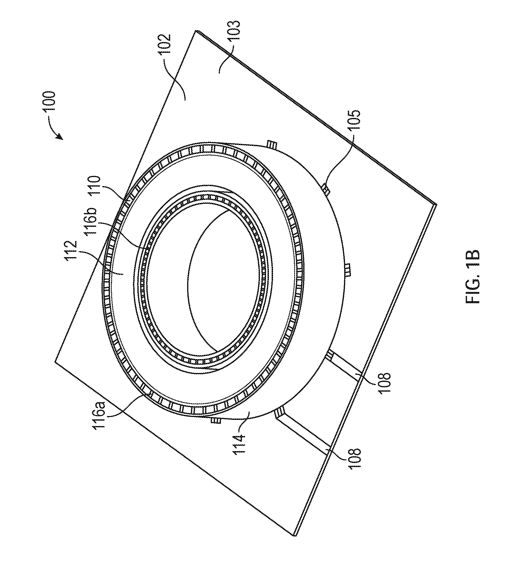
Referring to the drawings, FIGS. 1A-1C show an electrical device assembly 100. In the illustrated embodiment, the electrical device assembly 100 includes a lower printed wiring board 102, an upper printed wiring board 104, and a connector assembly 110. In the illustrated embodiment, the electrical device assembly 100 can be configured to operate as an inductor, transformer, etc. In the illustrated embodiment, the electrical device assembly 100 is shown as an inductor to filter input and output signals. Advantageously, the use of the connector assembly 110 allows for electrical connections needed for operation to be simplified.
In the illustrated embodiment, the electrical device assembly 100 allows for electrical connections to be formed in a desired arrangement. In the illustrated embodiment, the electrical device assembly 100 includes insulation barriers 114, an outer flexible connector 116a, a device core 112, and an inner flexible connector 116b. In the illustrated embodiment, the electrical device assembly 100 can be any suitable shape, including, but not limited to toroid shaped, etc.
In the illustrated embodiment, the outer flexible connector 116a and the inner flexible connector 116b are spaced apart with a device core 112 disposed therebetween. In the illustrated embodiment, the device core 112 is a solid core formed from any suitable material, including, but not limited to ferromagnetic materials. In certain embodiments, the device core 112 is an air core. Further, in the illustrated embodiment, insulation barriers 114 can be disposed around the outer flexible connector 116a and the inner flexible connector 116b to prevent unintended electrical connections within the electrical device assembly 100 and provide structural support.
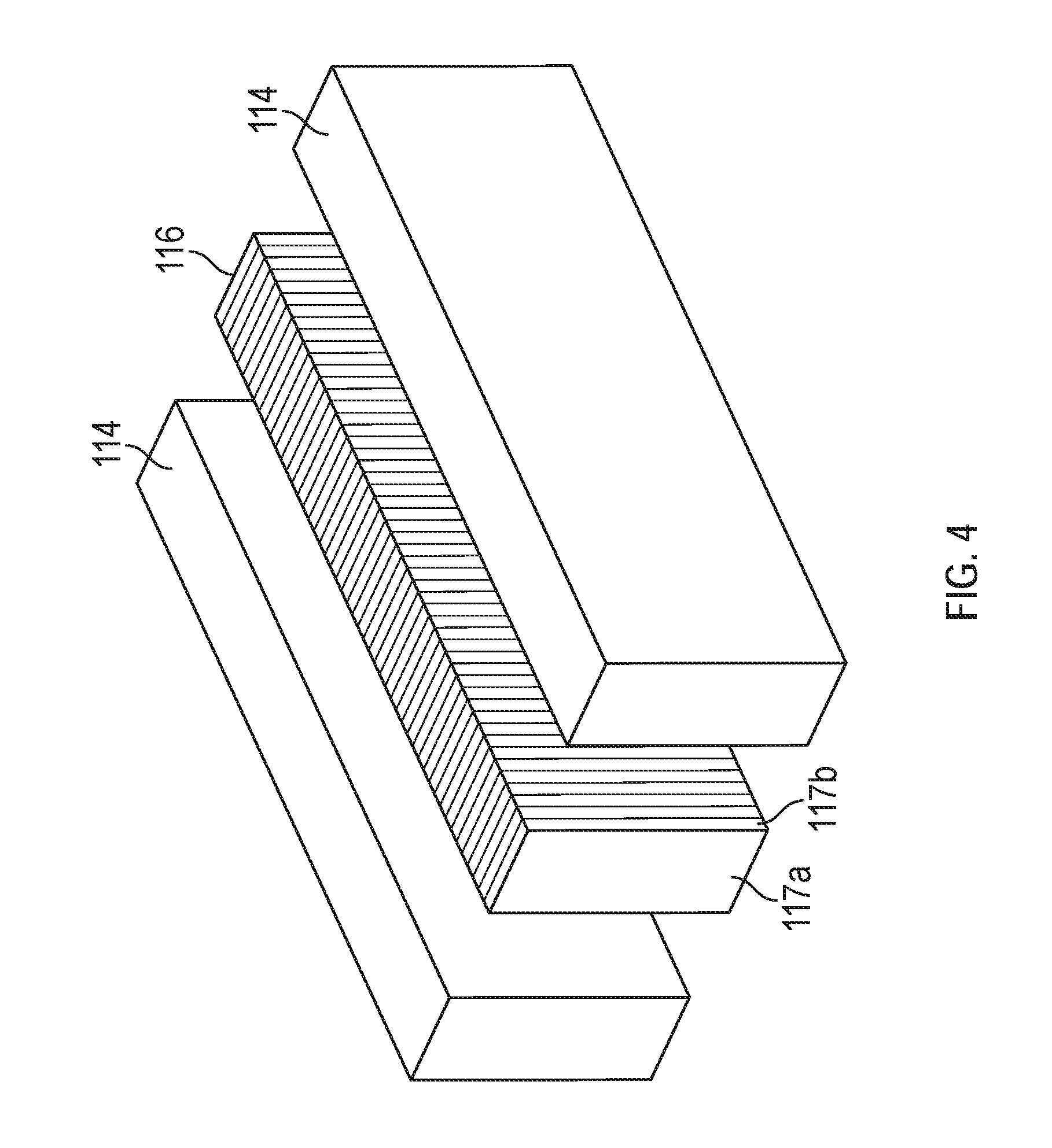
In the illustrated embodiment, electricity can flow within the flexible connectors 116a, 116b in a desired path to allow for a desired function, such as an inductor, transformer, etc. Referring to FIG. 4, each of the flexible connectors, generally referred to as flexible connector 116, includes alternating flexible conductors 117a and flexible insulators 117b. Advantageously, the flexible connector 116 provides a unitary body containing a plurality of flexible conductors 117a, allowing for conductive paths to be selectively created as desired quickly and inexpensively. Further, by utilizing flexible conductors 117a and flexible insulators 117b, the flexible connector 116 can withstand vibrations.
Referring back to FIGS. 1A-1C, the electrical device assembly 100 is disposed between the lower printed wiring board 102 and the upper wiring board 104. In the illustrated embodiment, the printed wiring boards 102,104 support and facilitate electrical connections through the electrical device assembly 100 to allow functionality as an inductor, transformer, etc.
Referring to FIGS. 1A-2, the lower printed wiring board 102 is shown. In the illustrated embodiment, the lower printed wiring board 102 includes contact pads 105, interconnects 106, and input/output traces 108. In the illustrated embodiment, the lower printed wiring board 102 is formed from any suitable printed wiring board material 103, including, but not limited to copper sheets laminated onto a non-conductive substrate.
In the illustrated embodiment, conductive interconnects 106 can be formed within the lower printed wiring board 102. The conductive interconnects 106 can be copper conductive pathways. In the illustrated embodiment, the interconnects 106 are embedded within the lower printed wiring board 102 and are otherwise insulated. In the illustrated embodiment, ends of the interconnect 106 include contact pads 105 that are formed on the surface of the lower printed wiring board 102. In the illustrated embodiment, the interconnect 106 allows electrical contact between one contact pad 105 and the opposite contact pad 105 on the opposite end of the interconnect 106. In the illustrated embodiment, the contact pads 105 and the interconnects 106 allow for electrical contact between conductors of the outer flexible connector 116a and the inner flexible connector 116b.
In the illustrated embodiment, the contact pads 105 are aligned with the conductors within the flexible connectors 116a, 116b to allow electrical contact between the conductors within the outer flexible connector 116a and the inner flexible connector 116b.
In the illustrated embodiment, input/output traces 108 can provide electricity into and out of the electrical device assembly 100. In the illustrated embodiment, the input/output traces 108 are electrically connected to select interconnects 106 to allow for electricity to flow through a desired path through the connector assembly 110.
Referring to FIGS. 1A-C and FIG. 3, the upper printed wiring board 104 is shown. In the illustrated embodiment, the upper printed wiring board 104 includes contact pads 105 and interconnects 106. In the illustrated embodiment, the upper printed wiring board 104 is formed from any suitable printed wiring board material 103, including, but not limited to copper sheets laminated onto a non-conductive substrate.
In the illustrated embodiment, conductive interconnects 106 can be formed within the upper printed wiring board 104. The conductive interconnects 106 can be copper conductive pathways. In the illustrated embodiment, the interconnects 106 are embedded within the upper printed wiring board 104 and are otherwise insulated. In the illustrated embodiment, ends of the interconnect 106 include contact pads 105 that are formed on the surface of the upper printed wiring board 104. In the illustrated embodiment, the contact pads 105 allow electrical contact between one contact pad 105 and the opposite contact pad 105 on the opposite end of the interconnect 106. In the illustrated embodiment, the contact pads 105 and the interconnects 106 allow for electrical contact between conductors within the outer flexible connector 116a and the inner flexible connector 116b.
In the illustrated embodiment, the contact pads 105 are aligned with the conductors within the flexible connectors 116a, 116b to allow electrical contact between the conductors within the outer flexible connector 116a and the inner flexible connector 116b.
Referring to FIG. 1C, in the illustrated embodiment, the lower printed wiring board 102 and the upper printed wiring board 104 facilitate desired electrical connections through the flexible connectors 116a,116b to allow the electrical device assembly 100 to function as desired. In the illustrated embodiment, the configuration of the lower printed wiring board 102, the upper printed wiring board 104, and the flexible connectors 116a, 116b allows for a coiled electrical path to allow for functionality as an inductor.
For example, in the illustrated embodiment, electrical current can flow into the electrical device assembly 100 via the input/output trace 108, wherein the input/output trace 108 is connected to an interconnect 106 (I.sub.Lower) disposed within the lower printed wiring board 102. In the illustrated embodiment, the contact pad 105 and the interconnect 106 (I.sub.Lower) are aligned within the lower printed wiring board 102 with the outer flexible connector 116a to allow a flexible conductor 117a (FIG. 4) (C.sub.Outer1) of the outer flexible conductor 116a to be electrically connected to the interconnect 106 (I.sub.Lower) within the lower printed wiring board 102. In the illustrated embodiment, the interconnect 106 (I.sub.Lower) is further electrically connected to the opposite contact pad 105, wherein the opposite contact pad 105 is aligned with a flexible conductor 117a (C.sub.Inner1) of the inner flexible connector 116b.
Similarly, in the illustrated embodiment, the contact pad 105 and the interconnect 106 (I.sub.Upper) within the upper printed wiring board 104 are aligned with the inner flexible connector 116b to allow the flexible conductor 117a (FIG. 4) (C.sub.Inner1) to be electrically connected to the interconnect 106 (T.sub.Upper) within the upper printed wiring board 104. In the illustrated embodiment, the interconnect 106 (T.sub.Upper) is electrically connected with the opposite contact pad 105, wherein the opposite contact pad 105 is aligned with the next or adjacent flexible conductor 117a (C.sub.Outer2) of the outer flexible connector 116a. Advantageously, this allows for a coil type power flow path without expensive and complex wiring configurations. In other embodiments, any suitable power flow path configuration can be utilized.
Referring to FIG. 5, in the illustrated embodiment, an electrical device assembly 200 is shown. In the illustrated embodiment, the electrical device assembly 200 is similar to the electrical device assembly 100 described herein, but further includes additional flexible connectors 116c, 116d. In the illustrated embodiment, the additional flexible connectors 116c, 116d can be utilized to provide additional current flow paths or to provide additional current capability. In certain embodiments, the flexible connector 116c can be wired in parallel with the outer flexible connector 116a to provide additional current capability. Similarly, the flexible connector 116d can be wired in parallel with the inner flexible connector 116b. In certain embodiments, the flexible connector 116c can be wired in series with the outer flexible connector 116a to provide additional looping current paths. Similarly, the flexible connector 116d can be wired in series with the inner flexible connector 116b. In other embodiments, the flexible connectors 116c, 116d can be wired in any suitable configuration.
The terminology used herein is for the purpose of describing particular embodiments only and is not intended to be limiting of the embodiments. While the description of the present embodiments has been presented for purposes of illustration and description, it is not intended to be exhaustive or limited to the embodiments in the form disclosed. Many modifications, variations, alterations, substitutions or equivalent arrangement not hereto described will be apparent to those of ordinary skill in the art without departing from the scope and spirit of the embodiments. Additionally, while various embodiments have been described, it is to be understood that aspects may include only some of the described embodiments. Accordingly, the embodiments are not to be seen as limited by the foregoing description, but are only limited by the scope of the appended claims.
* * * * *
D00000
D00001
D00002
D00003
D00004
D00005
D00006
D00007
XML
uspto.report is an independent third-party trademark research tool that is not affiliated, endorsed, or sponsored by the United States Patent and Trademark Office (USPTO) or any other governmental organization. The information provided by uspto.report is based on publicly available data at the time of writing and is intended for informational purposes only.
While we strive to provide accurate and up-to-date information, we do not guarantee the accuracy, completeness, reliability, or suitability of the information displayed on this site. The use of this site is at your own risk. Any reliance you place on such information is therefore strictly at your own risk.
All official trademark data, including owner information, should be verified by visiting the official USPTO website at www.uspto.gov. This site is not intended to replace professional legal advice and should not be used as a substitute for consulting with a legal professional who is knowledgeable about trademark law.