Fringe capacitance reduction for replacement gate CMOS
Niimi , et al. O
U.S. patent number 10,439,041 [Application Number 15/686,449] was granted by the patent office on 2019-10-08 for fringe capacitance reduction for replacement gate cmos. This patent grant is currently assigned to TEXAS INSTRUMENTS INCORPORATED. The grantee listed for this patent is Texas Instruments Incorporated. Invention is credited to Mahalingam Nandakumar, Hiroaki Niimi.


| United States Patent | 10,439,041 |
| Niimi , et al. | October 8, 2019 |
Fringe capacitance reduction for replacement gate CMOS
Abstract
A replacement metal gate transistor structure and method with thin silicon nitride sidewalls and with little or no high-k dielectric on the vertical sidewalls of the replacement gate transistor trench.
| Inventors: | Niimi; Hiroaki (Cohoes, NY), Nandakumar; Mahalingam (Richardson, TX) | ||||||||||
|---|---|---|---|---|---|---|---|---|---|---|---|
| Applicant: |
|
||||||||||
| Assignee: | TEXAS INSTRUMENTS INCORPORATED
(Dallas, TX) |
||||||||||
| Family ID: | 53482795 | ||||||||||
| Appl. No.: | 15/686,449 | ||||||||||
| Filed: | August 25, 2017 |
Prior Publication Data
| Document Identifier | Publication Date | |
|---|---|---|
| US 20170358659 A1 | Dec 14, 2017 | |
Related U.S. Patent Documents
| Application Number | Filing Date | Patent Number | Issue Date | ||
|---|---|---|---|---|---|
| 15093881 | Apr 8, 2016 | 9780192 | |||
| 14578722 | May 10, 2016 | 9337297 | |||
| 61922446 | Dec 31, 2013 | ||||
| Current U.S. Class: | 1/1 |
| Current CPC Class: | H01L 21/02178 (20130101); H01L 21/28238 (20130101); H01L 21/31055 (20130101); H01L 21/28167 (20130101); H01L 21/823857 (20130101); H01L 21/3212 (20130101); H01L 21/823842 (20130101); H01L 21/31053 (20130101); H01L 27/0922 (20130101); H01L 29/66545 (20130101); H01L 29/66553 (20130101); H01L 21/02186 (20130101); H01L 29/513 (20130101); H01L 21/02164 (20130101); H01L 21/31111 (20130101); H01L 21/32133 (20130101); H01L 21/02189 (20130101); H01L 29/517 (20130101); H01L 21/28194 (20130101); H01L 21/823456 (20130101); H01L 21/02181 (20130101); H01L 21/28123 (20130101); H01L 21/823468 (20130101); H01L 21/32 (20130101); H01L 21/0228 (20130101); H01L 29/42368 (20130101); H01L 29/4966 (20130101); H01L 29/7833 (20130101); H01L 29/495 (20130101); H01L 21/28088 (20130101); H01L 21/28079 (20130101) |
| Current International Class: | H01L 29/66 (20060101); H01L 21/8234 (20060101); H01L 29/49 (20060101); H01L 29/423 (20060101); H01L 29/78 (20060101); H01L 21/32 (20060101); H01L 21/8238 (20060101); H01L 27/092 (20060101); H01L 29/51 (20060101); H01L 21/3105 (20060101); H01L 21/3213 (20060101); H01L 21/311 (20060101); H01L 21/321 (20060101); H01L 21/02 (20060101); H01L 21/28 (20060101) |
References Cited [Referenced By]
U.S. Patent Documents
| 5880502 | March 1999 | Lee |
| 9012319 | April 2015 | Choi |
| 9337297 | May 2016 | Niimi |
| 2009/0189201 | July 2009 | Chang |
| 2012/0139062 | June 2012 | Yuan |
| 2012/0276702 | November 2012 | Yang |
Assistant Examiner: Lu; Farun
Attorney, Agent or Firm: Garner; Jacqueline J. Brill; Charles A. Cimino; Frank D.
Parent Case Text
CROSS-REFERENCE TO RELATED APPLICATIONS
This application is a continuation of U.S. Nonprovisional patent application Ser. No. 15/093,881, filed Apr. 8, 2016, which is a continuation of Ser. No. 14/578,722, filed Dec. 22, 2014 (now U.S. Pat. No. 9,337,297), which claims the benefit of U.S. provisional application Ser. No. 61/922,446, filed Dec. 31, 2013, the contents of all of which are herein incorporated by reference in its entirety.
Claims
What is claimed is:
1. An integrated circuit with a metal gate transistor comprising: a replacement gate transistor trench; silicon nitride sidewalls with a thickness of less than about 0.3 nm on vertical sidewalls of the replacement gate transistor trench; high-k gate dielectric, w herein a thickness of the high-k gate dielectric on the vertical sidewalls of the replacement gate transistor trench is less than half a thickness of the high-k gate dielectric over a bottom surface of the replacement gate transistor trench; and metal gate material covering the high-k gate dielectric and filling the replacement gate transistor trench.
2. The integrated circuit of claim 1, wherein the high-k gate dielectric is HfOx, HfSiOx, HfSiON, ZrO.sub.2, HfZrOx, AlOx, or TiOx.
3. The integrated circuit of claim 1, wherein the metal gate transistor is an NMOS transistor, the high-k gate dielectric is HfOx, and the metal gate material is selected from the group titanium, aluminum, titanium-aluminum alloy, and tungsten.
4. The integrated circuit of claim 1, wherein the metal gate transistor is a PMOS transistor, the high-k gate dielectric is HfOx, and the metal gate material is selected from the group consisting of titanium nitride, tantalum nitride, aluminum, and platinum.
5. An integrated circuit comprising: a first gate trench of a first metal gate transistor; a silicon nitride layer with a first thickness on sidewalls of the first gate trench; a high-k gate dielectric, wherein a second thickness of the high-k gate dielectric on the sidewalls of the first gate trench that is less than half a third thickness of the high-k gate dielectric over a bottom surface of the first pate trench, wherein the first thickness is less than the third thickness; and a first metal gate material covering the high-k gate dielectric and filling the first gate trench.
6. The integrated circuit of claim 5, wherein the high-k gate dielectric is HfOx, HfSiOx, HfSiON, ZrO.sub.2, HfZrOx, AlOx, or TiOx.
7. The integrated circuit of claim 5, wherein the first metal gate transistor is an NMOS transistor, the high-k gate dielectric is HfOx, and the first metal gate material is selected from the group titanium, aluminum, titanium-aluminum alloy, and tungsten.
8. The integrated circuit of claim 5, wherein the first metal gate transistor is an PMOS transistor, the high-k gate dielectric is HfOx, and the first metal gate material is selected from the group consisting of titanium nitride, tantalum nitride, aluminum, and platinum.
9. The integrated circuit of claim 5, further comprising a second gate trench of a second transistor, wherein the second gate trench includes: the silicon nitride layer; the high-k gate dielectric; and a second metal gate material covering the high-k gate dielectric in the second gate trench and filling the second gate trench.
10. The integrated circuit of claim 9, wherein: the first metal gate transistor is an NMOS transistor, the high-k gate dielectric is HfOx, and the first metal gate material is selected from the group titanium, aluminum, titanium-aluminum alloy, and tungsten; and the second metal gate transistor is a PMOS transistor and the second metal gate material is selected from the group consisting of titanium nitride, tantalum nitride, aluminum, and platinum.
11. The integrated circuit of claim 5, further comprising a gate oxide dielectric under the high-k gate dielectric in the first gate trench.
12. An integrated circuit comprising: a first metal gate transistor comprising: a first gate trench; a silicon nitride layer with a first thickness on sidewalls of the first gate trench; a high-k gate dielectric, wherein a second thickness of the high-k gate dielectric on the sidewalls of the first gate trench that is less than half a third thickness of the high-k gate dielectric over a bottom surface of the first gate trench, wherein the first thickness is less than the third thickness; and a first metal gate material covering the high-k gate dielectric and filling the first gate trench; a second metal gate transistor comprising: a second gate trench wider than the first gate trench; the silicon nitride layer on sidewalls of the second gate trench; the high-k gate dielectric, wherein the second thickness of the high-k gate dielectric on the sidewalls of the second gate trench that is less than half the third thickness of the high-k gate dielectric over a bottom surface of the second gate trench; and the first metal gate material covering the high-k gate dielectric and filling the second gate trench; a third metal gate transistor comprising: a third gate trench; the silicon nitride layer on sidewalls of the third gate trench; the high-k gate dielectric, wherein the second thickness of the high-k gate dielectric on the sidewalls of the third gate trench that is less than half the third thickness of the high-k gate dielectric over a bottom surface of the third gate trench; and a second metal gate material covering the high-k gate dielectric in the third trench and filling the third gate trench; and a fourth metal gate transistor comprising: a fourth gate trench wider than the third gate trench; the silicon nitride layer on sidewalls of the fourth gate trench; the high-k gate dielectric, wherein the second thickness of the high-k gate dielectric on the sidewalls of the fourth gate trench that is less than half the third thickness of the high-k gate dielectric over a bottom surface of the fourth gate trench; and the second metal gate material covering the high-k gate dielectric in the fourth gate trench and filling the fourth gate trench.
13. The integrated circuit of claim 12, wherein the high-k gate dielectric is HfOx, HfSiOx, HfSiON, ZrO.sub.2, HfZrOx, AlOx, or TiOx.
14. The integrated circuit of claim 12, wherein the first metal gate transistor and the second metal gate transistors are NMOS transistors, the high-k gate dielectric is HfOx, and the first metal gate material is selected from the group titanium, aluminum, titanium-aluminum alloy, and tungsten.
15. The integrated circuit of claim 14, wherein the third metal gate transistor and fourth metal gate transistor are PMOS transistors and the second metal gate material is selected from the group consisting of titanium nitride, tantalum nitride, aluminum, and platinum.
16. The integrated circuit of claim 12, further comprising: a first gate oxide dielectric under the high-k gate dielectric in the first gate trench and the third gate trench; and a second gate oxide dielectric under the high-k gate dielectric in the second gate trench and the fourth gate trench.
Description
FIELD OF INVENTION
This invention relates to the field of integrated circuits. More particularly, this invention relates to replacement gate transistors in integrated circuits.
BACKGROUND
As the geometries for integrated circuits have scaled to smaller and smaller dimensions, it has become necessary to replace polysilicon transistor gates with metal gates to enable scaling to continue to smaller dimensions. When voltage is applied to a polysilicon gate the polysilicon grains next to the gate dielectric become depleted of carriers increasing the electrical thickness of the gate dielectric and exacerbating short channel effects. Metal gates do not deplete when voltage is applied to the metal gate.
Because the work function of most p-channel metal-oxide-semiconductor (PMOS) metal gate material changes when the metal gate is subjected to high temperatures such as is required to activate dopants, replacement gate processes have been developed to circumvent the work function problem. In a replacement gate process, transistors are first built in the usual manner using polysilicon gates and silicon dioxide gate dielectric. The polysilion gates and gate dielectric are then removed and replaced with high-k gate dielectric and metal gates. Typically after removal of the polysilicon replacement gate, high-k dielectric is deposited followed by metal gate deposition. The high-k dielectric typically deposits conformally on the sidewalls and bottom of the trench formed by removal of the polysilicon replacement gate. Metal gate material is then deposited to fill the trench.
Because of the high dielectric constant of the high-k dielectric on the sidewalls of the trench, fringe capacitance is increased which degrades transistor performance.
In addition, gate geometries have been scaled to such small dimensions (i.e., less than 30 nm) that when the trench width is reduced by the high-k dielectric deposition, it is difficult to completely fill the trench without forming voids.
SUMMARY
The following presents a simplified summary in order to provide a basic understanding of one or more aspects of the invention. This summary is not an extensive overview of the invention, and is neither intended to identify key or critical elements of the invention, nor to delineate the scope thereof. Rather, the primary purpose of the summary is to present some concepts of the invention in a simplified form as a prelude to a more detailed description that is presented later.
A replacement metal gate transistor structure and method for forming with thin silicon nitride sidewalls and with little or no high-k dielectric on the vertical sidewalls of the replacement gate transistor trench.
BRIEF DESCRIPTION OF THE DRAWINGS
FIGS. 1A-1K are illustrations of steps in the fabrication of integrated circuits formed according to principles of the invention.
DETAILED DESCRIPTION OF EXAMPLE EMBODIMENTS
The present invention is described with reference to the attached FIGURES. The figures are not drawn to scale and they are provided merely to illustrate the invention. Several aspects of the invention are described below with reference to example applications for illustration. It should be understood that numerous specific details, relationships, and methods are set forth to provide an understanding of the invention. One skilled in the relevant art, however, will readily recognize that the invention can be practiced without one or more of the specific details or with other methods. In other instances, well-known structures or operations are not shown in detail to avoid obscuring the invention. The present invention is not limited by the illustrated ordering of acts or events, as some acts may occur in different orders and/or concurrently with other acts or events. Furthermore, not all illustrated acts or events are required to implement a methodology in accordance with the present invention.
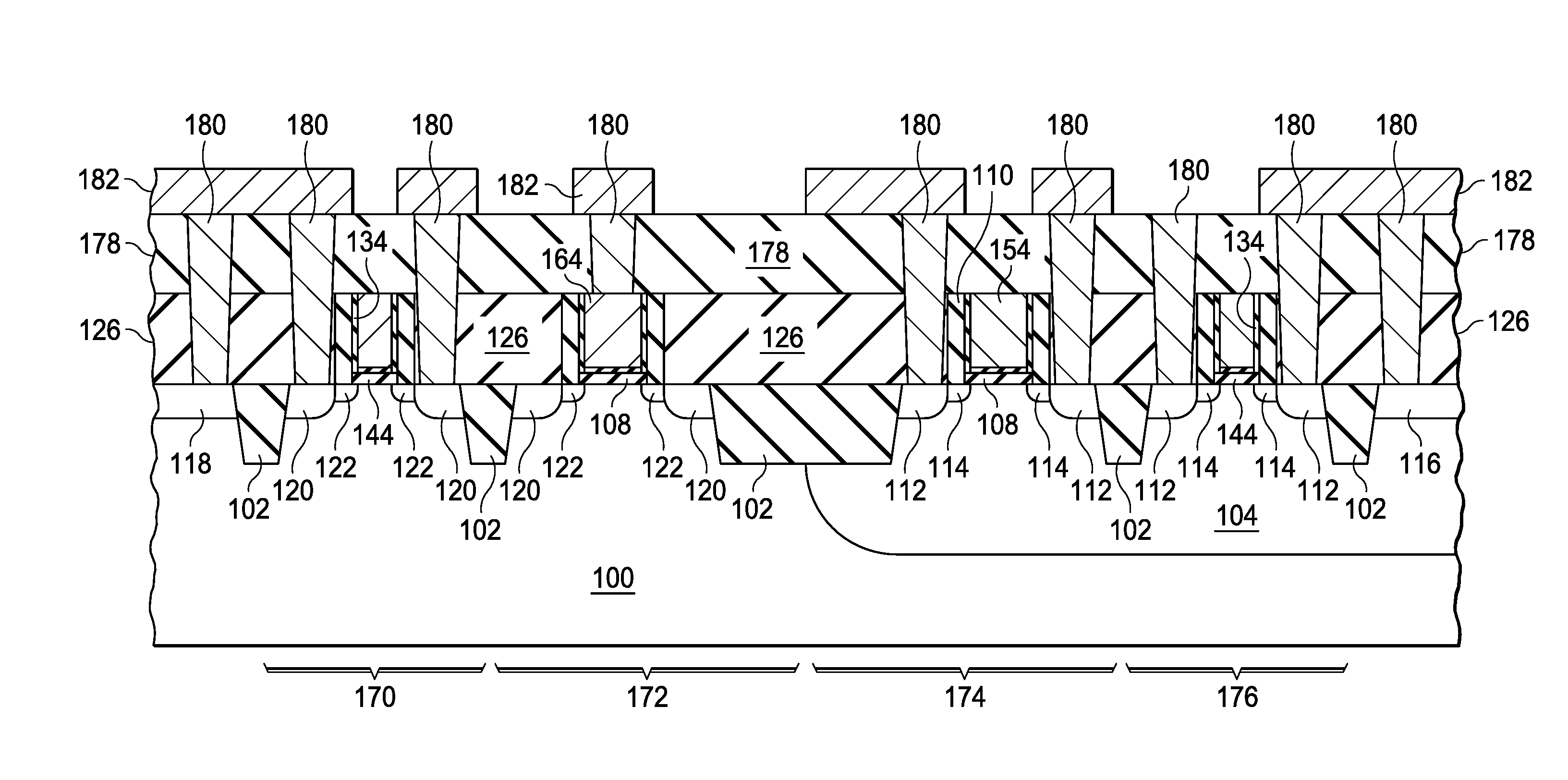
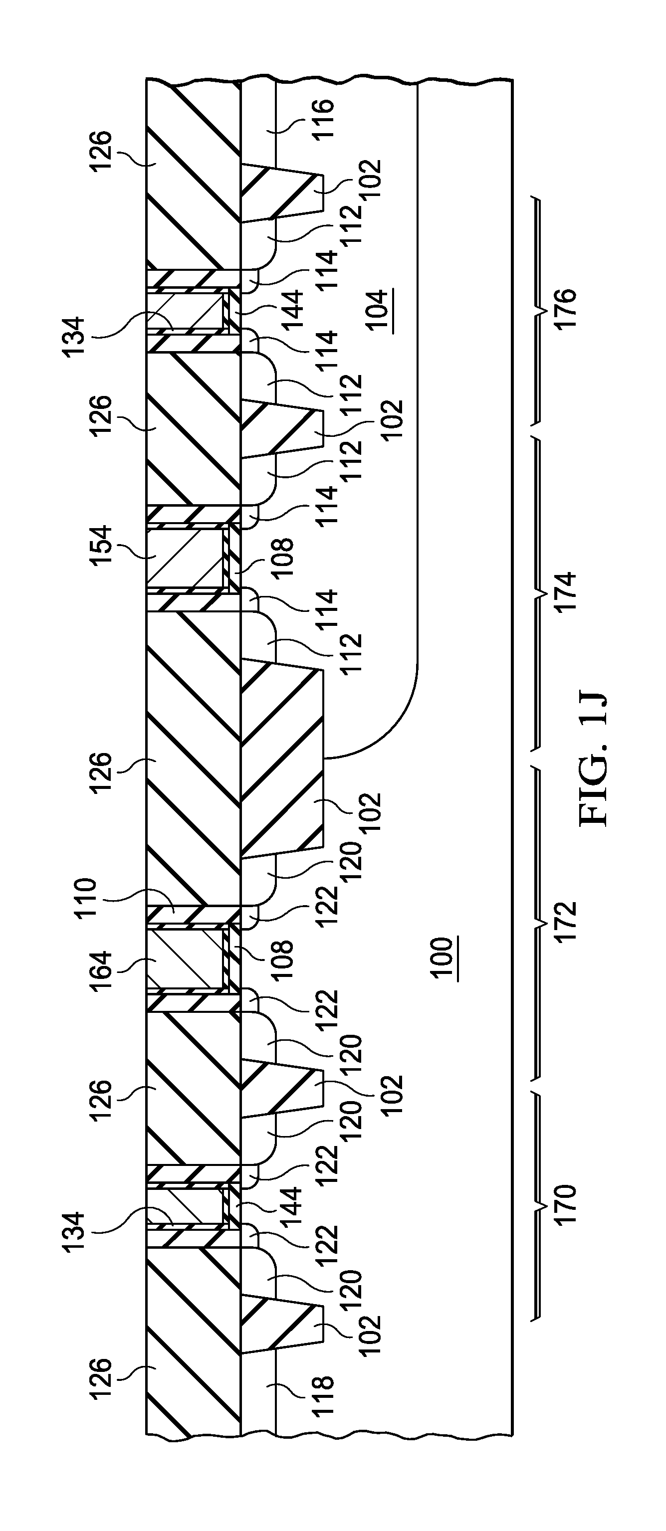
An integrated circuit formed using embodiments of the invention which reduces deposition of high-k dielectric on the sidewalls of the replacement gate transistor trench is shown in FIG. 1J. Thin sidewalls 134 of silicon nitride are formed on the vertical sides of the replacement gate transistor trenches prior to high-k gate dielectric 150 deposition. The thin silicon nitride sidewalls 134 blocks high-k dielectric 150 nucleation and thereby significantly reduces the deposition of high-k gate dielectric 150 on the vertical sidewalls of the replacement gate transistor trenches. A reduced thickness of high-k gate dielectric 150 on the sidewalls reduces fringe capacitance thereby improving transistor performance. In addition the reduced high-k thickness on the trench sidewalls increases the width of the trench improving the ability of the metal gate material to completely fill the replacement gate transistor trench without forming voids.
An example process flow that builds n-channel metal-oxide-semiconductor (NMOS) and p-channel metal-oxide-semiconductor (PMOS), high voltage and low voltage replacement gate transistors using embodiments is illustrated in FIGS. 1A through 1K.
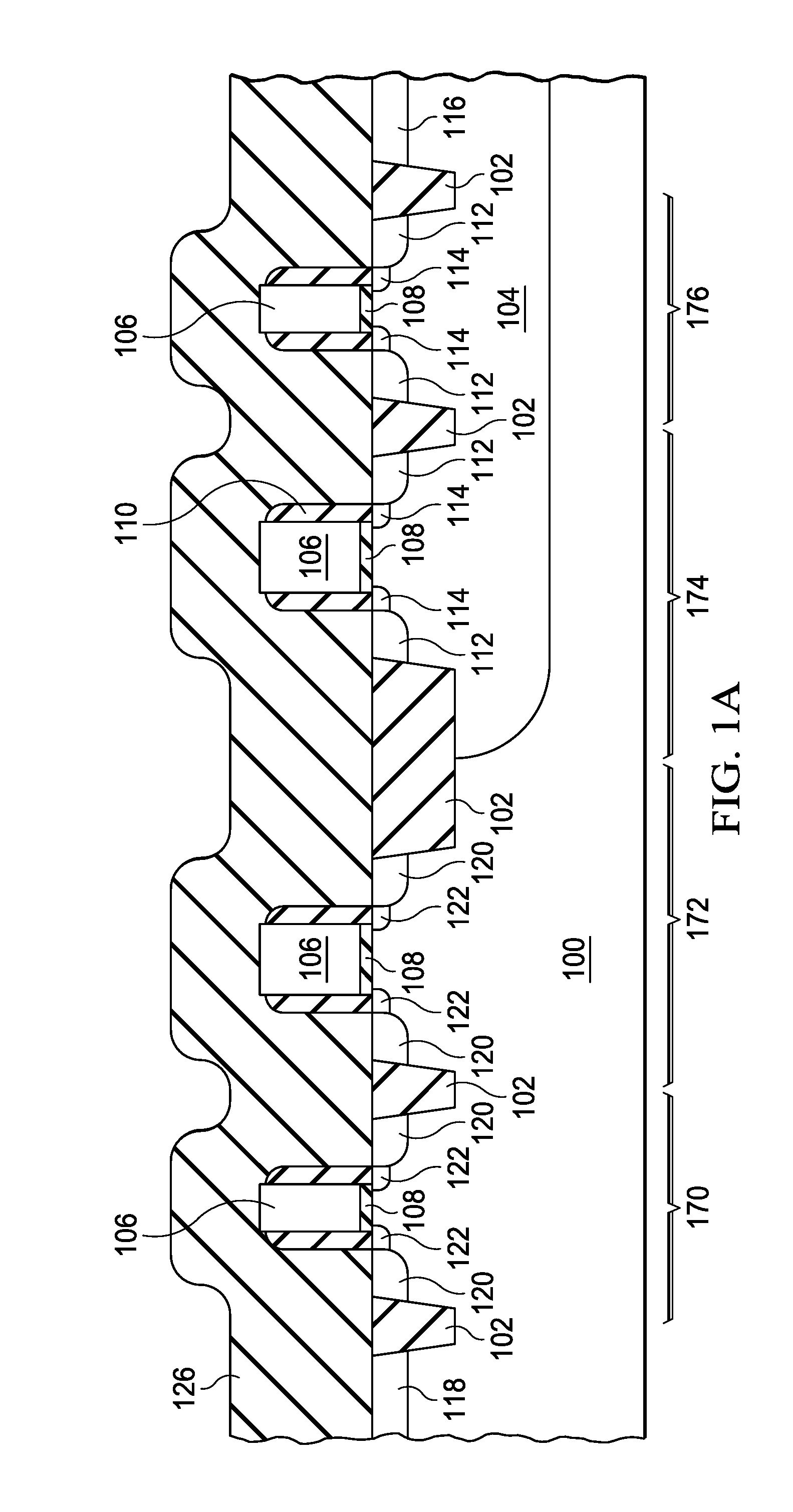
FIG. 1A is a cross section of a partially processed integrated circuit with NMOS low voltage 170 and NMOS high voltage 172 transistors and PMOS low voltage 176 and PMOS high voltage 174 transistors.
In this example embodiment, the NMOS transistors 170 and 172 are formed in p-type substrate 100 and PMOS transistors 174 and 176 are formed in an nwell 104. Shallow trench isolation 102 electrically isolates the transistors from each other. Polysilicon transistor gates 106 are formed on a gate dielectric 108 such as silicon dioxide or nitrided silicon dioxide. N-type source and drain extensions 122 are formed self aligned to the polysilicon gates on the NMOS transistors 170 and 172 and p-type source and drain extensions 114 are formed self aligned to the polysilicon gates on the PMOS transistors 174 and 176. N-type deep source and drain diffusions 120 are formed self-aligned to the sidewalls 110 on the NMOS transistors 170 and 172 and p-type deep source and drain diffusions 112 are formed self-aligned to the sidewalls 110 on the PMOS transistors 174 and 176. The sidewalls 110 may be silicon dioxide to reduce fringe capacitance. Replacement gate dielectric 126 covers the transistors on the integrated circuit so that the surface of the replacement gate dielectric 126 is at least the height of the polysilicon transistor gates.
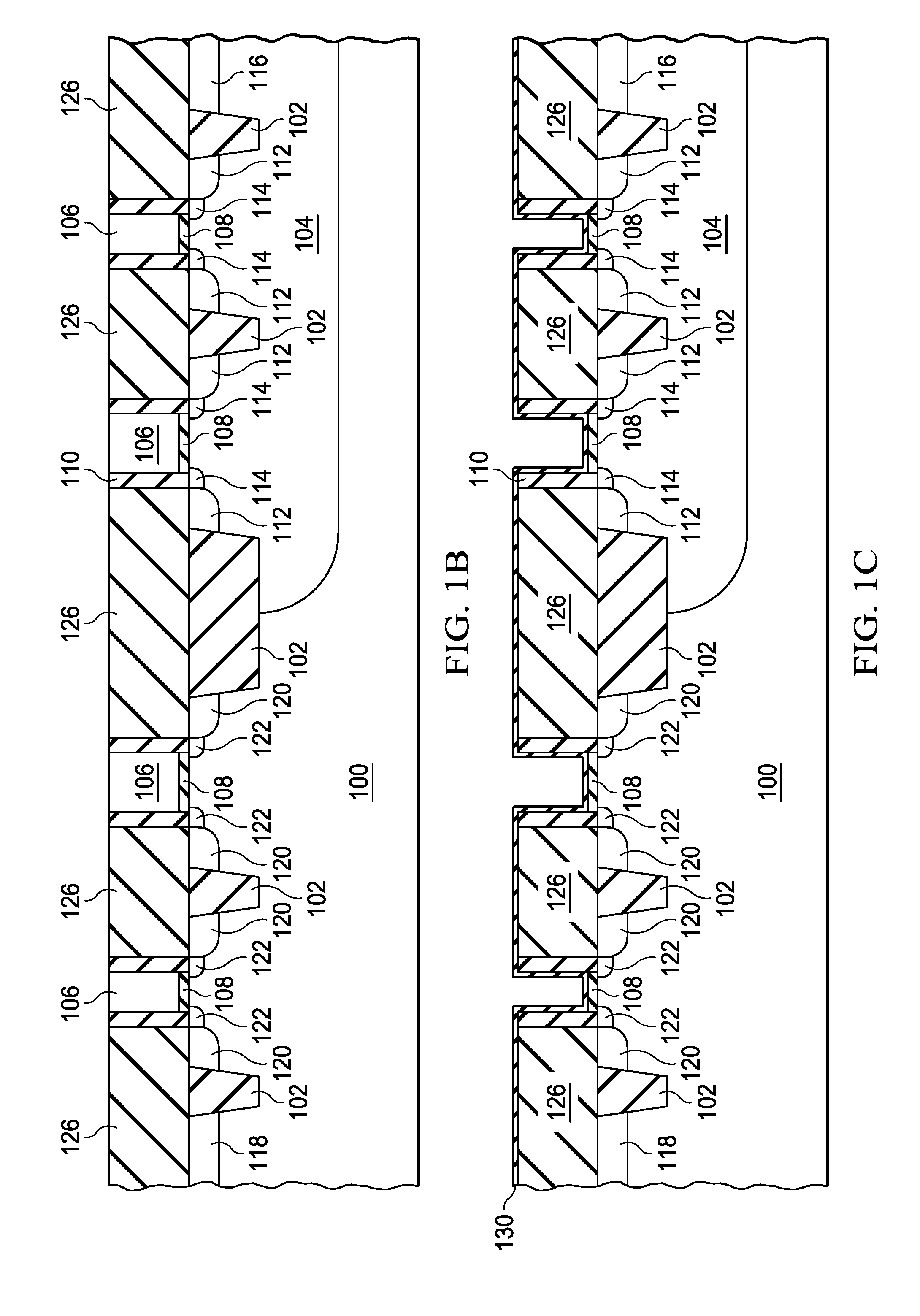
Referring now to FIG. 1B, chemical mechanical polish (CMP) is used to planarize the dielectric 126 and to expose the tops of the polysilicon replacement gates 106.
As shown in FIG. 1C, the polysilicon replacement gates are removed and a thin layer 130 of silicon nitride is formed on the surface of the dielectric 126 and on the surfaces of the replacement gate transistor trenches. The silicon nitride may be formed using atomic layer deposition (ALD) techniques or may be formed using plasma nitridation to form a thin layer 130 of silicon nitride on silicon dioxide sidewalls 110. The silicon nitride layer may be about 0.05 to 0.3 nm thick.
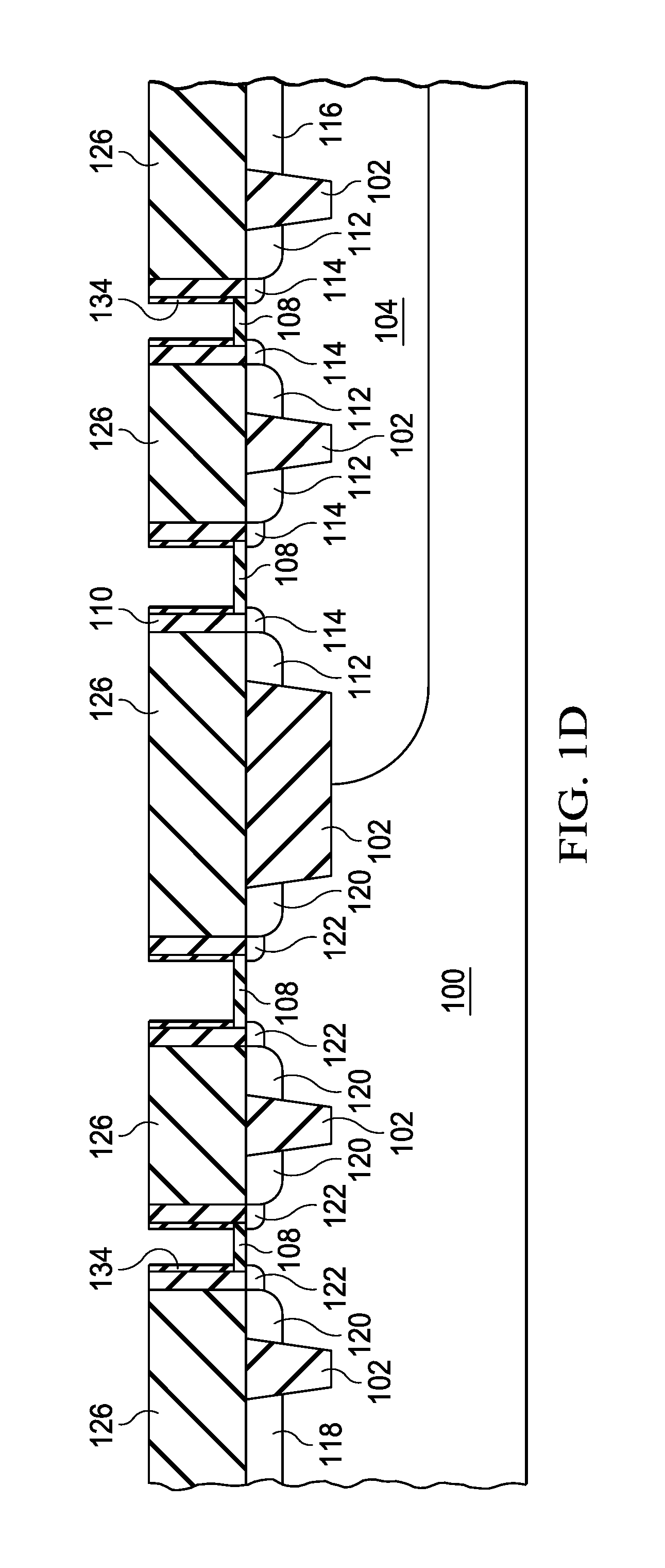
As illustrated in FIG. 1D, an anisotropic plasma etch may be used to remove the thin silicon nitride layer 130 from the horizontal surfaces on the replacement gate dielectric 126 and the bottom of the replacement gate trenches and leaving silicon nitride sidewalls 134 and 136 on the vertical sides of the replacement gate transistor trenches.
In FIG. 1E a high voltage photo resist pattern 140 is formed on the integrated circuit to prevent the gate dielectric 108 from being removed from the high voltage transistor, 172 and 174 trenches. The gate oxide dielectric 108 is removed from the bottom of the low voltage transistor, 170 and 176 trenches.
Referring now to FIG. 1F, gate oxide dielectric 144 is formed in the low voltage transistor trenches 170 and 176, and high-k dielectric 150 is deposited. The gate oxide dielectric 144 may be grown using SCl (NH.sub.4OH+ H.sub.2O.sub.2) wet chemistry. In an example embodiment, approximately 0.6 nm SiO.sub.x 144 is chemically grown using SCl. The high-k dielectric 150 may be a high-k dielectric such as HfO.sub.x, HfSiO.sub.x, HfSiON, ZrO.sub.2, HFZrO.sub.x, AlO.sub.x, and TiO.sub.x in the range of about 1 to 4 nm thick. In an example embodiment approximately 1.5 nm HfO.sub.x is deposited using atomic layer deposition (ALD). The thin silicon nitride sidewalls 134 and 136 on the vertical sidewalls of the replacement gate transistor trenches retards high-k dielectric nucleation 150 the thickness of the high-k dielectric 150 thickness on the sidewalls of the replacement gate transistor trench is less than half the thickness of the high-k dielectric on the bottom of the trench. In most instances little or no high-k dielectric 150 is deposited on the sidewalls. Since little or no high-k dielectric 150 is deposited on the sidewalls of the trenches, little of the width of the trenches is reduced by deposited high-k dielectric. This enables the metal gate material to be deposited without trapping voids. In addition, fringe capacitance is reduced since the silicon nitride sidewalls 134 and 136 are thinner than high-k dielectric and the dielectric constant of silicon nitride is much lower than the dielectric constant of high-k dielectrics.
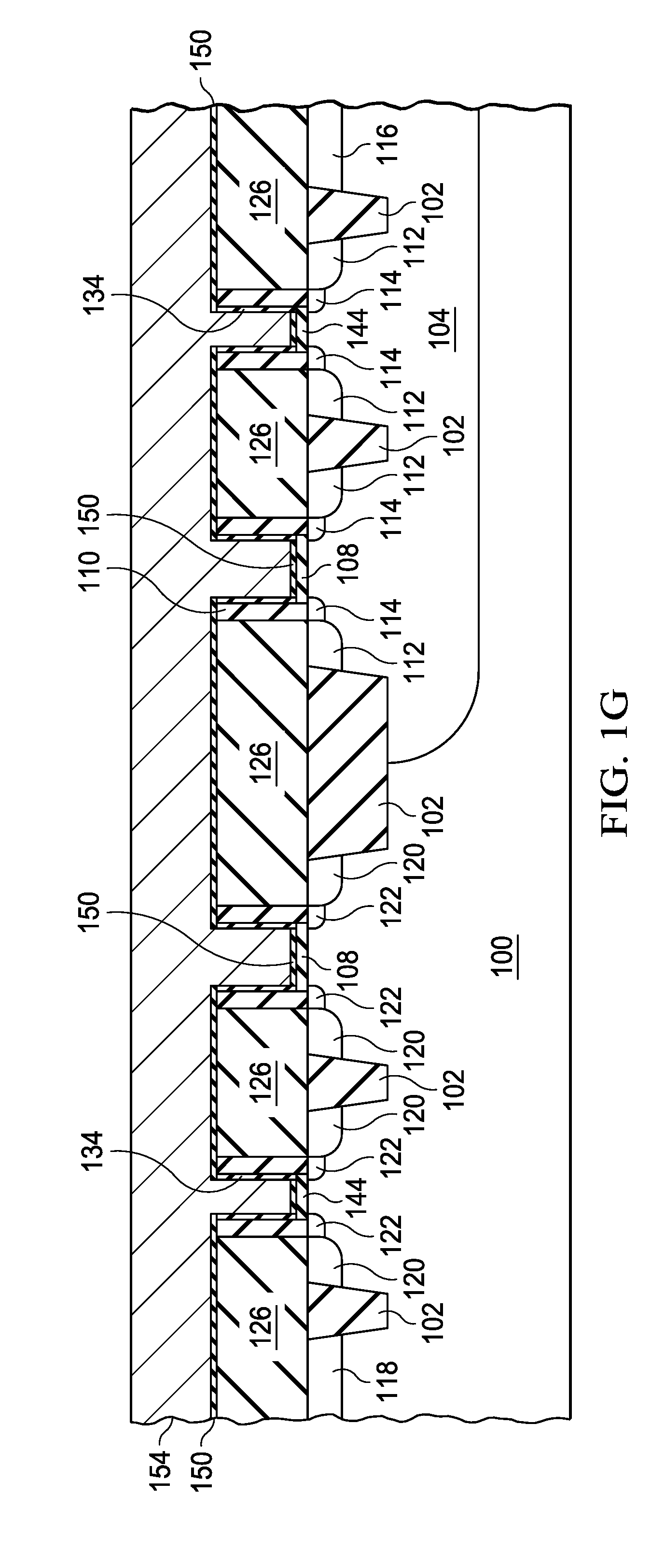
As shown in FIG. 1G, PMOS metal gate material 154 is then deposited into the replacement gate trenches. The PMOS metal gate material 154 may contain for example, one or more metals from the group consisting of titanium nitride, tantalum nitride, aluminum, and platinum. The trenches are wider because the high-k dielectric is thinner on the vertical sidewalls making the trenches easier to fill without the formation of voids. In an example embodiment the PMOS metal gate material 154 is about 8 nm of titanium nitride.
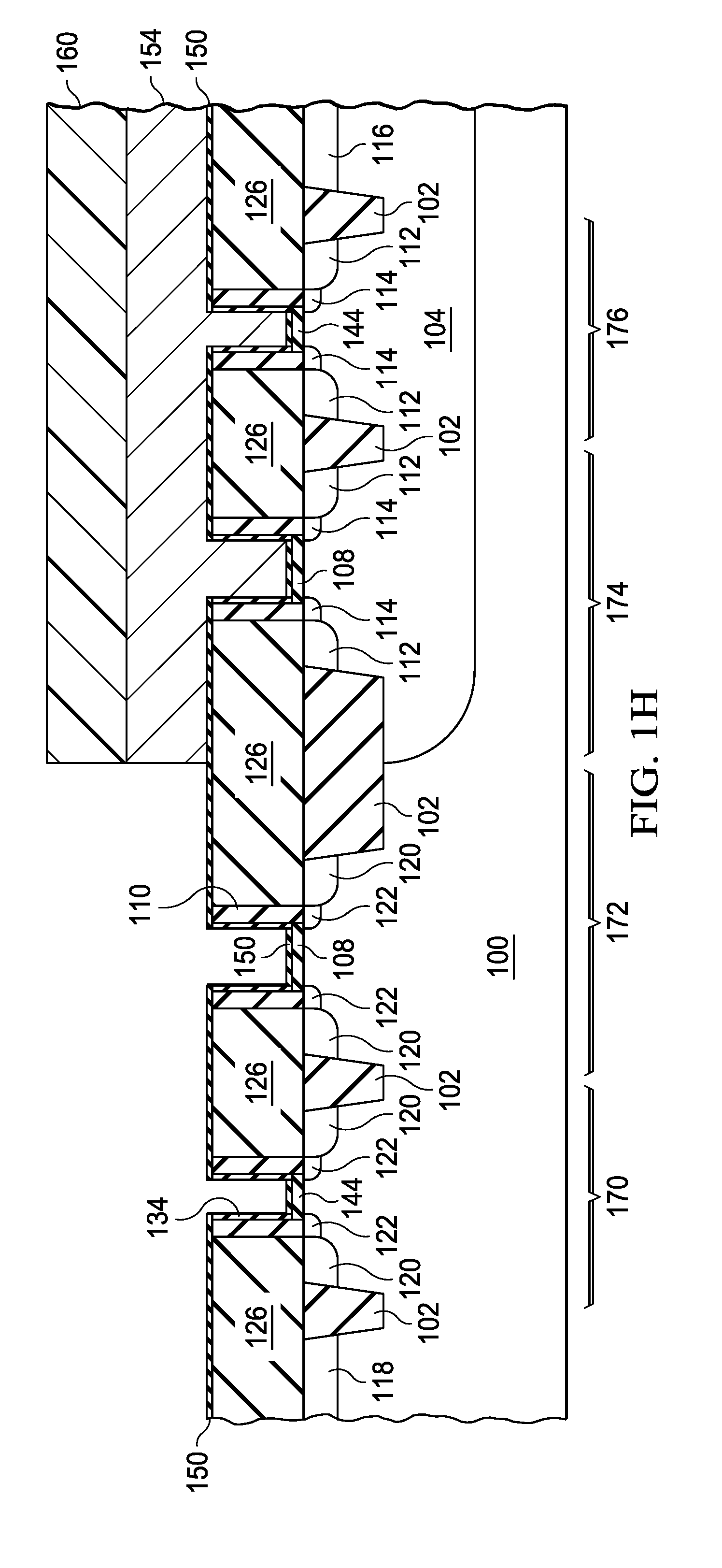
In FIG. 1H PMOS metal gate photo resist pattern 160 is formed on the integrated circuit to prevent the PMOS metal gate material 154 from being removed over the PMOS transistors, 174 and 176. The PMOS metal gate material 154 is removed from the NMOS transistors, 170 and 172.
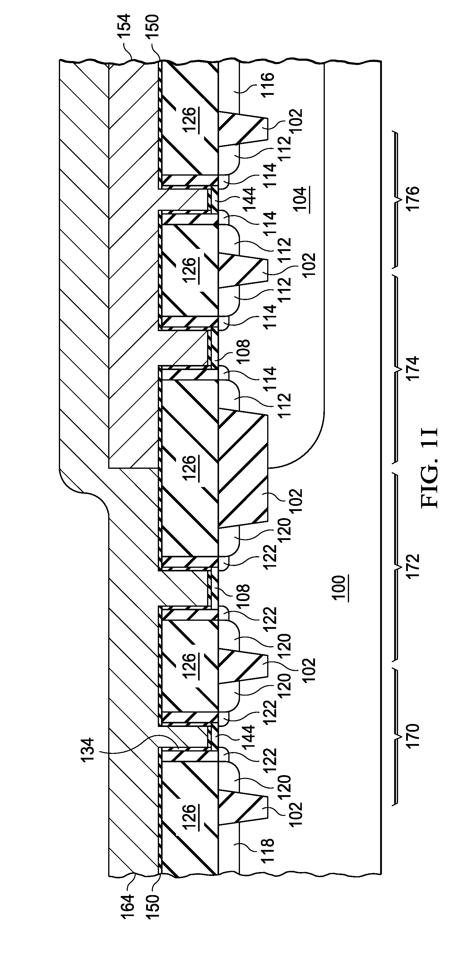
Referring now to FIG. 1I, a NMOS transistor metal gate material 164 is deposited into the NMOS transistor, 170 and 172, replacement gate trenches. The trenches are wider because the high-k dielectric is thinner on the vertical sidewalls making the trenches easier to fill without the formation of voids. The NMOS metal gate material 164 may contain for example, one or more metals from the group consisting of titanium, aluminum, titanium-aluminum alloy, and tungsten. In an example embodiment the NMOS metal gate material 164 is about 3 nm of titanium-aluminum alloy.
CMP is used to remove the NMOS metal gate material 164 overfill and the PMOS metal gate material 154 overfill from the surface of the replacement gate dielectric 126 as shown in FIG. 1J.
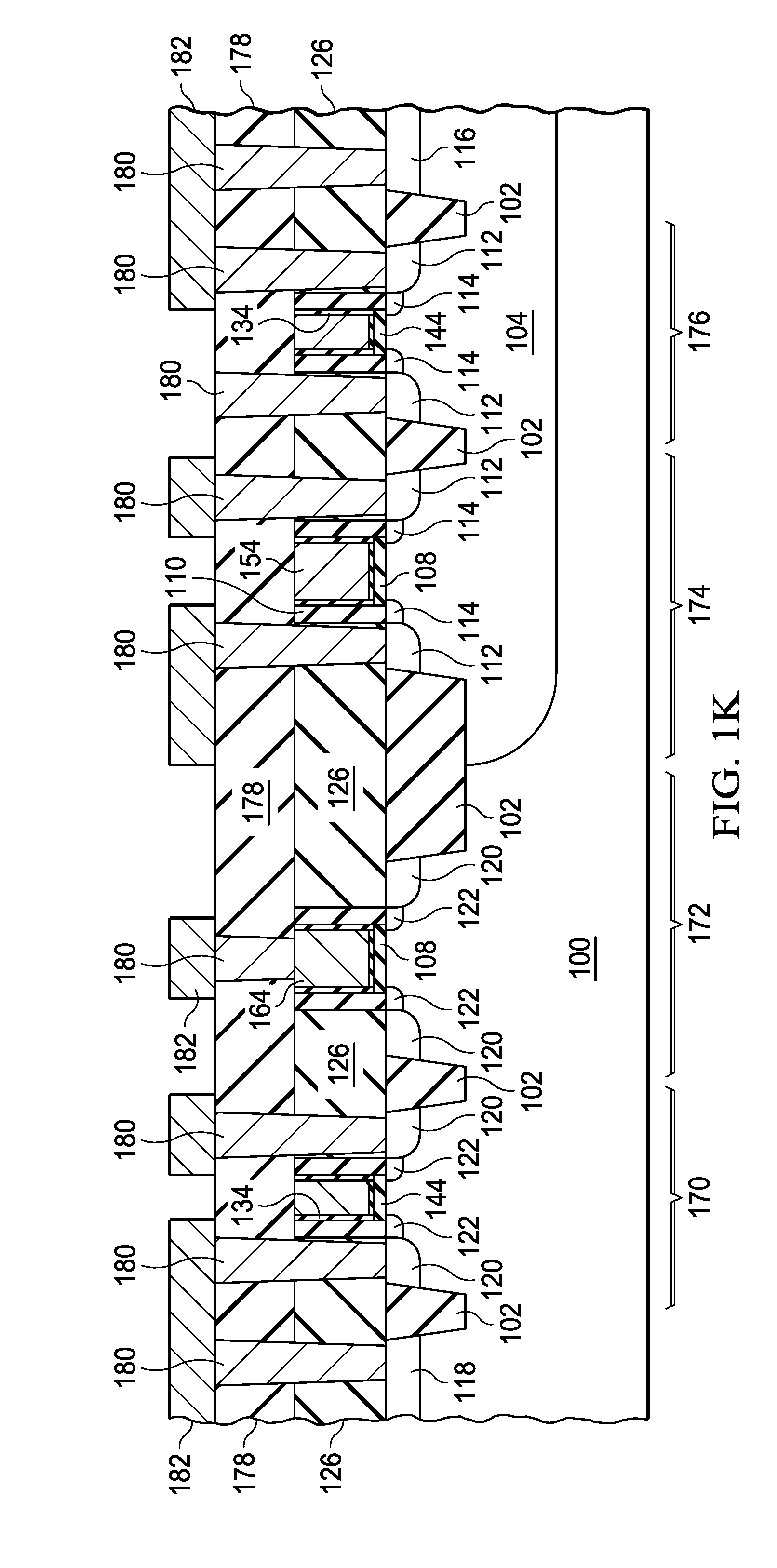
In FIG. 1K, a premetal dielectric layer (PMD) 178 may be deposited on the integrated circuit and contact plugs 180 formed through the PMD 178 and replacement gate dielectric 126 to affect electrical connection between the deep source and drain diffusions, 112 and 120, and the first layer of interconnect 182. Additional layers of dielectric and interconnect electrically connected by vias may be formed over the first layer of interconnect 182 to complete the integrated circuit.
Those skilled in the art to which this invention relates will appreciate that many other embodiments and variations are possible within the scope of the claimed invention.
* * * * *
D00000
D00001
D00002
D00003
D00004
D00005
D00006
D00007
D00008
D00009
D00010
XML
uspto.report is an independent third-party trademark research tool that is not affiliated, endorsed, or sponsored by the United States Patent and Trademark Office (USPTO) or any other governmental organization. The information provided by uspto.report is based on publicly available data at the time of writing and is intended for informational purposes only.
While we strive to provide accurate and up-to-date information, we do not guarantee the accuracy, completeness, reliability, or suitability of the information displayed on this site. The use of this site is at your own risk. Any reliance you place on such information is therefore strictly at your own risk.
All official trademark data, including owner information, should be verified by visiting the official USPTO website at www.uspto.gov. This site is not intended to replace professional legal advice and should not be used as a substitute for consulting with a legal professional who is knowledgeable about trademark law.