Electrically isolated heat dissipating junction box
Sella , et al. Sept
U.S. patent number 10,411,644 [Application Number 15/651,134] was granted by the patent office on 2019-09-10 for electrically isolated heat dissipating junction box. This patent grant is currently assigned to Solaredge Technologies, Ltd.. The grantee listed for this patent is Solaredge Technologies Ltd.. Invention is credited to Meir Adest, Yoav Galin, Meir Gazit, Lior Handelsman, Guy Sella, Vadim Shmukler.

| United States Patent | 10,411,644 |
| Sella , et al. | September 10, 2019 |
Electrically isolated heat dissipating junction box
Abstract
A junction box used for making electrical connections to a photovoltaic panel. The junction box has two chambers including a first chamber and a second chamber and a wall common to and separating both chambers. The wall may be adapted to have an electrical connection therethrough. The two lids are adapted to seal respectively the two chambers. The two lids are on opposite sides of the junction box relative to the photovoltaic panel. The two lids may be attachable using different sealing processes to a different level of hermeticity. The first chamber may be adapted to receive a circuit board for electrical power conversion. The junction box may include supports for mounting a printed circuit board in the first chamber. The second chamber is configured for electrical connection to the photovoltaic panel. A metal heat sink may be bonded inside the first chamber.
| Inventors: | Sella; Guy (Bitan Aharon, IL), Handelsman; Lior (Givataim, IL), Shmukler; Vadim (Rishon-Lezion, IL), Adest; Meir (Raanana, IL), Gazit; Meir (Ashkelon, IL), Galin; Yoav (Raanana, IL) | ||||||||||
|---|---|---|---|---|---|---|---|---|---|---|---|
| Applicant: |
|
||||||||||
| Assignee: | Solaredge Technologies, Ltd.
(Herzeliya, IL) |
||||||||||
| Family ID: | 42668129 | ||||||||||
| Appl. No.: | 15/651,134 | ||||||||||
| Filed: | July 17, 2017 |
Prior Publication Data
| Document Identifier | Publication Date | |
|---|---|---|
| US 20180069505 A1 | Mar 8, 2018 | |
Related U.S. Patent Documents
| Application Number | Filing Date | Patent Number | Issue Date | ||
|---|---|---|---|---|---|
| 14997079 | Jan 15, 2016 | 9748897 | |||
| 14641690 | Mar 9, 2015 | 9748896 | |||
| 13901706 | Apr 14, 2015 | 9006569 | |||
| 12785773 | Jul 2, 2013 | 8476524 | |||
| 61180455 | May 22, 2009 | ||||
| Current U.S. Class: | 1/1 |
| Current CPC Class: | H05K 7/2039 (20130101); G08B 13/1409 (20130101); H05K 5/02 (20130101); H02G 15/10 (20130101); H05K 9/0015 (20130101); H05K 9/0007 (20130101); H05K 9/0009 (20130101); H02S 40/34 (20141201); H02S 40/345 (20141201); H05K 5/062 (20130101); Y10S 248/906 (20130101); Y10T 29/49117 (20150115) |
| Current International Class: | H02S 40/34 (20140101); H05K 9/00 (20060101); H02G 15/10 (20060101); H05K 7/20 (20060101); G08B 13/14 (20060101); H05K 5/02 (20060101); H05K 5/06 (20060101) |
| Field of Search: | ;174/50 |
References Cited [Referenced By]
U.S. Patent Documents
| 3369210 | February 1968 | Manickella |
| 3596229 | July 1971 | Hohorst |
| 4060757 | November 1977 | McMurray |
| 4101816 | July 1978 | Shepter |
| 4171861 | October 1979 | Hohorst |
| 4452867 | June 1984 | Conforti |
| 4460232 | July 1984 | Sotolongo |
| 4481654 | November 1984 | Daniels et al. |
| 4598330 | July 1986 | Woodworth |
| 4623753 | November 1986 | Feldman et al. |
| 4637677 | January 1987 | Barkus |
| 4641042 | February 1987 | Miyazawa |
| 4641079 | February 1987 | Kato et al. |
| 4644458 | February 1987 | Harafuji et al. |
| 4652770 | March 1987 | Kumano |
| 4783728 | November 1988 | Hoffman |
| RE33057 | September 1989 | Clegg et al. |
| 4868379 | September 1989 | West |
| 4888063 | December 1989 | Powell |
| 4888702 | December 1989 | Gerken et al. |
| 4899269 | February 1990 | Rouzies |
| 4945559 | July 1990 | Collins |
| 4987360 | January 1991 | Thompson |
| 5045988 | September 1991 | Gritter et al. |
| 5081558 | January 1992 | Mahler |
| 5191519 | March 1993 | Kawakami |
| 5280232 | January 1994 | Kohl et al. |
| 5327071 | July 1994 | Frederick et al. |
| 5345375 | September 1994 | Mohan |
| 5391235 | February 1995 | Inoue |
| 5402060 | March 1995 | Erisman |
| 5446645 | August 1995 | Shirahama et al. |
| 5460546 | October 1995 | Kunishi et al. |
| 5493154 | February 1996 | Smith et al. |
| 5497289 | March 1996 | Sugishima et al. |
| 5517378 | May 1996 | Asplund et al. |
| 5548504 | August 1996 | Takehara |
| 5604430 | February 1997 | Decker et al. |
| 5616913 | April 1997 | Litterst |
| 5644219 | July 1997 | Kurokawa |
| 5646501 | July 1997 | Fishman et al. |
| 5659465 | August 1997 | Flack et al. |
| 5686766 | November 1997 | Tamechika |
| 5726505 | March 1998 | Yamada et al. |
| 5773963 | June 1998 | Blanc et al. |
| 5780092 | July 1998 | Agbo et al. |
| 5798631 | August 1998 | Spee et al. |
| 5801519 | September 1998 | Midya et al. |
| 5804894 | September 1998 | Leeson et al. |
| 5821734 | October 1998 | Faulk |
| 5822186 | October 1998 | Bull et al. |
| 5838148 | November 1998 | Kurokami et al. |
| 5869956 | February 1999 | Nagao et al. |
| 5873738 | February 1999 | Shimada et al. |
| 5892354 | April 1999 | Nagao et al. |
| 5905645 | May 1999 | Cross |
| 5919314 | July 1999 | Kim |
| 5923158 | July 1999 | Kurokami et al. |
| 5932994 | August 1999 | Jo et al. |
| 5945806 | August 1999 | Faulk |
| 5949668 | September 1999 | Schweighofer |
| 5963010 | October 1999 | Hayashi et al. |
| 5990659 | November 1999 | Frannhagen |
| 6031736 | February 2000 | Takehara et al. |
| 6038148 | March 2000 | Farrington et al. |
| 6046919 | April 2000 | Madenokouji et al. |
| 6050779 | April 2000 | Nagao et al. |
| 6078511 | June 2000 | Fasullo et al. |
| 6081104 | June 2000 | Kern |
| 6082122 | July 2000 | Madenokouji et al. |
| 6111188 | August 2000 | Kurokami et al. |
| 6111391 | August 2000 | Cullen |
| 6111767 | August 2000 | Handleman |
| 6163086 | December 2000 | Choo |
| 6166455 | December 2000 | Li |
| 6166527 | December 2000 | Dwelley et al. |
| 6169678 | January 2001 | Kondo et al. |
| 6219623 | April 2001 | Wills |
| 6255360 | July 2001 | Domschke et al. |
| 6259234 | July 2001 | Perol |
| 6262558 | July 2001 | Weinberg |
| 6285572 | September 2001 | Onizuka et al. |
| 6301128 | October 2001 | Jang et al. |
| 6304065 | October 2001 | Wittenbreder |
| 6320769 | November 2001 | Kurokami et al. |
| 6339538 | January 2002 | Handleman |
| 6344612 | February 2002 | Kuwahara et al. |
| 6351130 | February 2002 | Preiser et al. |
| 6369462 | April 2002 | Sin |
| 6380719 | April 2002 | Underwood et al. |
| 6396170 | May 2002 | Laufenberg et al. |
| 6433522 | August 2002 | Sin |
| 6448489 | September 2002 | Kimura et al. |
| 6452814 | September 2002 | Wittenbreder |
| 6493246 | December 2002 | Suzui et al. |
| 6507176 | January 2003 | Wittenbreder, Jr. |
| 6531848 | March 2003 | Chitsazan et al. |
| 6545211 | April 2003 | Mimura |
| 6548205 | April 2003 | Leung et al. |
| 6590793 | July 2003 | Nagao et al. |
| 6593521 | July 2003 | Kobayashi |
| 6600100 | July 2003 | Ho et al. |
| 6608468 | August 2003 | Nagase |
| 6611441 | August 2003 | Kurokami et al. |
| 6628011 | September 2003 | Droppo et al. |
| 6650560 | November 2003 | MacDonald et al. |
| 6653549 | November 2003 | Matsushita et al. |
| 6655987 | December 2003 | Higashikozono et al. |
| 6678174 | January 2004 | Suzui et al. |
| 6690590 | February 2004 | Stamenic et al. |
| 6738692 | May 2004 | Schienbein et al. |
| 6765315 | July 2004 | Hammerstrom et al. |
| 6768047 | July 2004 | Chang et al. |
| 6788033 | September 2004 | Vinciarelli |
| 6795318 | September 2004 | Haas et al. |
| 6801442 | October 2004 | Suzui et al. |
| 6828503 | December 2004 | Yoshikawa et al. |
| 6850074 | February 2005 | Adams et al. |
| 6882131 | April 2005 | Takada et al. |
| 6914418 | July 2005 | Sung |
| 6919714 | July 2005 | Delepaut |
| 6927955 | August 2005 | Suzui et al. |
| 6933627 | August 2005 | Wilhelm |
| 6936995 | August 2005 | Kapsokavathis et al. |
| 6950323 | September 2005 | Achleitner et al. |
| 6963147 | November 2005 | Kurokami et al. |
| 6984967 | January 2006 | Notman |
| 6984970 | January 2006 | Capel |
| 7030597 | April 2006 | Bruno et al. |
| 7031176 | April 2006 | Kotsopoulos et al. |
| 7042195 | May 2006 | Tsunetsugu et al. |
| 7046531 | May 2006 | Zocchi et al. |
| 7053506 | May 2006 | Alonso et al. |
| 7072194 | July 2006 | Nayar et al. |
| 7079406 | July 2006 | Kurokami et al. |
| 7087332 | August 2006 | Harris |
| 7090509 | August 2006 | Gilliland et al. |
| 7091707 | August 2006 | Cutler |
| 7097516 | August 2006 | Werner et al. |
| 7126053 | October 2006 | Kurokami et al. |
| 7126294 | October 2006 | Minami et al. |
| 7138786 | November 2006 | Ishigaki et al. |
| 7148669 | December 2006 | Maksimovic et al. |
| 7154755 | December 2006 | Araujo |
| 7158359 | January 2007 | Bertele et al. |
| 7158395 | January 2007 | Deng et al. |
| 7174973 | February 2007 | Lysaght |
| 7193872 | March 2007 | Siri |
| 7218541 | May 2007 | Price et al. |
| 7248946 | July 2007 | Bashaw et al. |
| 7256566 | August 2007 | Bhavaraju et al. |
| 7277304 | October 2007 | Stancu et al. |
| 7282814 | October 2007 | Jacobs |
| 7291036 | November 2007 | Daily et al. |
| RE39976 | January 2008 | Schiff et al. |
| 7336056 | February 2008 | Dening |
| 7352154 | April 2008 | Cook |
| 7371963 | May 2008 | Suenaga et al. |
| 7372712 | May 2008 | Stancu et al. |
| 7385380 | June 2008 | Ishigaki et al. |
| 7385833 | June 2008 | Keung |
| 7394237 | July 2008 | Chou et al. |
| 7420815 | September 2008 | Love |
| 7471014 | December 2008 | Lum et al. |
| 7589437 | September 2009 | Henne et al. |
| 7622802 | November 2009 | Paulus et al. |
| 7646116 | January 2010 | Batarseh et al. |
| 7719140 | May 2010 | Ledenev et al. |
| 7759575 | July 2010 | Jones et al. |
| 7763807 | July 2010 | Richter |
| 7772716 | August 2010 | Shaver, II et al. |
| 7782031 | August 2010 | Qiu et al. |
| 7787273 | August 2010 | Lu et al. |
| 7804282 | September 2010 | Bertele |
| 7812701 | October 2010 | Lee et al. |
| 7824189 | November 2010 | Lauermann et al. |
| 7868599 | January 2011 | Rahman et al. |
| 7880334 | February 2011 | Evans et al. |
| 7893346 | February 2011 | Nachamkin et al. |
| 7948221 | May 2011 | Watanabe et al. |
| 7952897 | May 2011 | Nocentini et al. |
| 7960650 | June 2011 | Richter et al. |
| 8003885 | August 2011 | Richter et al. |
| 8035249 | October 2011 | Shaver, II et al. |
| 8097818 | January 2012 | Gerull et al. |
| 8204709 | June 2012 | Presher, Jr. et al. |
| 8222533 | July 2012 | Gherardini et al. |
| 8248804 | August 2012 | Han et al. |
| 8289183 | October 2012 | Foss |
| 8294451 | October 2012 | Hasenfus |
| 8303349 | November 2012 | Shmukler |
| 8324921 | December 2012 | Adest et al. |
| 8378656 | February 2013 | de Rooij et al. |
| 8410950 | April 2013 | Takehara et al. |
| 8427009 | April 2013 | Shaver, II et al. |
| 8710351 | April 2014 | Robbins |
| 8785771 | July 2014 | Dunkleberger et al. |
| 8816535 | August 2014 | Adest et al. |
| 8823218 | September 2014 | Hadar et al. |
| 8835748 | September 2014 | Frolov et al. |
| 8878563 | November 2014 | Robbins |
| 8963375 | February 2015 | DeGraaff |
| 2002/0044473 | April 2002 | Toyomura et al. |
| 2002/0056089 | May 2002 | Houston |
| 2003/0058593 | March 2003 | Bertele et al. |
| 2003/0066076 | April 2003 | Minahan |
| 2003/0075211 | April 2003 | Makita et al. |
| 2003/0080741 | May 2003 | LeRow et al. |
| 2003/0214274 | November 2003 | Lethellier |
| 2004/0041548 | March 2004 | Perry |
| 2004/0125618 | July 2004 | De Rooij et al. |
| 2004/0140719 | July 2004 | Vulih et al. |
| 2004/0169499 | September 2004 | Huang et al. |
| 2004/0201279 | October 2004 | Templeton |
| 2004/0201933 | October 2004 | Blanc |
| 2004/0246226 | December 2004 | Moon |
| 2005/0002214 | January 2005 | Deng et al. |
| 2005/0005785 | January 2005 | Poss et al. |
| 2005/0017697 | January 2005 | Capel |
| 2005/0057214 | March 2005 | Matan |
| 2005/0057215 | March 2005 | Matan |
| 2005/0068820 | March 2005 | Radosevich et al. |
| 2005/0099138 | May 2005 | Wilhelm |
| 2005/0103376 | May 2005 | Matsushita et al. |
| 2005/0162018 | July 2005 | Realmuto et al. |
| 2005/0172995 | August 2005 | Rohrig et al. |
| 2005/0226017 | October 2005 | Kotsopoulos et al. |
| 2006/0001406 | January 2006 | Matan |
| 2006/0017327 | January 2006 | Siri et al. |
| 2006/0034106 | February 2006 | Johnson |
| 2006/0038692 | February 2006 | Schnetker |
| 2006/0053447 | March 2006 | Krzyzanowski et al. |
| 2006/0068239 | March 2006 | Norimatsu et al. |
| 2006/0108979 | May 2006 | Daniel et al. |
| 2006/0113843 | June 2006 | Beveridge |
| 2006/0113979 | June 2006 | Ishigaki et al. |
| 2006/0118162 | June 2006 | Saelzer et al. |
| 2006/0132102 | June 2006 | Harvey |
| 2006/0149396 | July 2006 | Templeton |
| 2006/0162772 | July 2006 | Presher et al. |
| 2006/0163946 | July 2006 | Henne et al. |
| 2006/0171182 | August 2006 | Siri et al. |
| 2006/0174939 | August 2006 | Matan |
| 2006/0185727 | August 2006 | Matan |
| 2006/0192540 | August 2006 | Balakrishnan et al. |
| 2006/0208660 | September 2006 | Shinmura et al. |
| 2006/0227578 | October 2006 | Datta et al. |
| 2006/0235717 | October 2006 | Sharma et al. |
| 2006/0237058 | October 2006 | McClintock et al. |
| 2007/0044837 | March 2007 | Simburger et al. |
| 2007/0075711 | April 2007 | Blanc et al. |
| 2007/0081364 | April 2007 | Andreycak |
| 2007/0159866 | July 2007 | Siri |
| 2007/0164750 | July 2007 | Chen et al. |
| 2007/0165347 | July 2007 | Wendt et al. |
| 2007/0205778 | September 2007 | Fabbro et al. |
| 2007/0227574 | October 2007 | Cart |
| 2007/0236187 | October 2007 | Wai et al. |
| 2007/0273342 | November 2007 | Kataoka et al. |
| 2008/0024098 | January 2008 | Hojo |
| 2008/0088184 | April 2008 | Tung et al. |
| 2008/0097655 | April 2008 | Hadar et al. |
| 2008/0106250 | May 2008 | Prior et al. |
| 2008/0142071 | June 2008 | Dorn et al. |
| 2008/0143188 | June 2008 | Adest et al. |
| 2008/0143462 | June 2008 | Belisle et al. |
| 2008/0147335 | June 2008 | Adest et al. |
| 2008/0150366 | June 2008 | Adest et al. |
| 2008/0179949 | July 2008 | Besser et al. |
| 2008/0236647 | October 2008 | Gibson et al. |
| 2008/0236648 | October 2008 | Klein et al. |
| 2008/0238195 | October 2008 | Shaver et al. |
| 2008/0246460 | October 2008 | Smith |
| 2008/0246463 | October 2008 | Sinton et al. |
| 2008/0291609 | November 2008 | Victor et al. |
| 2009/0073726 | March 2009 | Babcock |
| 2009/0084570 | April 2009 | Gherardini et al. |
| 2009/0097172 | April 2009 | Bremicker et al. |
| 2009/0102440 | April 2009 | Coles |
| 2009/0141522 | June 2009 | Adest et al. |
| 2009/0182532 | July 2009 | Stoeber et al. |
| 2009/0190275 | July 2009 | Gilmore et al. |
| 2009/0242011 | October 2009 | Proisy et al. |
| 2009/0283129 | November 2009 | Foss |
| 2009/0325003 | December 2009 | Aberle et al. |
| 2010/0020576 | January 2010 | Falk |
| 2010/0071742 | March 2010 | de Rooij et al. |
| 2010/0124087 | May 2010 | Falk |
| 2010/0139743 | June 2010 | Hadar et al. |
| 2010/0154858 | June 2010 | Jain |
| 2010/0206378 | August 2010 | Erickson, Jr. et al. |
| 2010/0214808 | August 2010 | Rodriguez |
| 2010/0241375 | September 2010 | Kumar et al. |
| 2010/0244575 | September 2010 | Coccia et al. |
| 2010/0301991 | December 2010 | Sella et al. |
| 2011/0006743 | January 2011 | Fabbro |
| 2011/0043172 | February 2011 | Dearn |
| 2011/0068633 | March 2011 | Quardt et al. |
| 2011/0108087 | May 2011 | Croft et al. |
| 2011/0125431 | May 2011 | Adest et al. |
| 2011/0133552 | June 2011 | Binder et al. |
| 2011/0198935 | August 2011 | Hinman et al. |
| 2011/0240100 | October 2011 | Lu et al. |
| 2011/0254372 | October 2011 | Haines et al. |
| 2011/0267859 | November 2011 | Chapman |
| 2011/0290317 | December 2011 | Naumovitz et al. |
| 2012/0043818 | February 2012 | Stratakos et al. |
| 2012/0080943 | April 2012 | Phadke |
| 2012/0138123 | June 2012 | Newdoll et al. |
| 2012/0139343 | June 2012 | Adest et al. |
| 2012/0194003 | August 2012 | Schmidt et al. |
| 2012/0199172 | August 2012 | Avrutsky |
| 2013/0038124 | February 2013 | Newdoll et al. |
| 2013/0049710 | February 2013 | Kraft et al. |
| 2013/0082724 | April 2013 | Noda et al. |
| 2013/0321013 | December 2013 | Pisklak et al. |
| 86200903 | Jan 1987 | CN | |||
| 1236213 | Nov 1999 | CN | |||
| 1577980 | Feb 2005 | CN | |||
| 1578034 | Feb 2005 | CN | |||
| 1700480 | Nov 2005 | CN | |||
| 1933315 | Mar 2007 | CN | |||
| 200941388 | Aug 2007 | CN | |||
| 101192744 | Jun 2008 | CN | |||
| 101388530 | Mar 2009 | CN | |||
| 201207557 | Mar 2009 | CN | |||
| 201238275 | May 2009 | CN | |||
| 101951190 | Jan 2011 | CN | |||
| 101953051 | Jan 2011 | CN | |||
| 19737286 | Mar 1999 | DE | |||
| 10219956 | Apr 2003 | DE | |||
| 102004053942 | May 2006 | DE | |||
| 102005036153 | Dec 2006 | DE | |||
| 102005030907 | Jan 2007 | DE | |||
| 102007051134 | Mar 2009 | DE | |||
| 102007037130 | Apr 2009 | DE | |||
| 202009007318 | Aug 2009 | DE | |||
| 102008057874 | May 2010 | DE | |||
| 102009051186 | May 2010 | DE | |||
| 102009022569 | Dec 2010 | DE | |||
| 419093 | Mar 1991 | EP | |||
| 420295 | Apr 1991 | EP | |||
| 604777 | Jul 1994 | EP | |||
| 756178 | Jan 1997 | EP | |||
| 827254 | Mar 1998 | EP | |||
| 1039361 | Sep 2000 | EP | |||
| 1330009 | Jul 2003 | EP | |||
| 1503490 | Feb 2005 | EP | |||
| 1531545 | May 2005 | EP | |||
| 1657557 | May 2006 | EP | |||
| 1657797 | May 2006 | EP | |||
| 1887675 | Feb 2008 | EP | |||
| 2048679 | Apr 2009 | EP | |||
| 2130286 | Dec 2009 | EP | |||
| 2135296 | Dec 2009 | EP | |||
| 2256819 | Dec 2010 | EP | |||
| 2249147 | Mar 2006 | ES | |||
| 2249149 | Mar 2006 | ES | |||
| 2128017 | Apr 1984 | GB | |||
| 2480015 | Nov 2011 | GB | |||
| 61065320 | Apr 1986 | JP | |||
| H10308523 | Nov 1998 | JP | |||
| 11041832 | Feb 1999 | JP | |||
| 11103538 | Apr 1999 | JP | |||
| 2003124492 | Apr 2003 | JP | |||
| 2003134667 | May 2003 | JP | |||
| 2003282916 | Oct 2003 | JP | |||
| 2006278755 | Oct 2006 | JP | |||
| 2007058845 | Mar 2007 | JP | |||
| 4174227 | Oct 2008 | JP | |||
| 200913291 | Mar 2009 | TW | |||
| 1993013587 | Jul 1993 | WO | |||
| 1996013093 | May 1996 | WO | |||
| 1998023021 | May 1998 | WO | |||
| 00/00839 | Jan 2000 | WO | |||
| 00/21178 | Apr 2000 | WO | |||
| 0075947 | Dec 2000 | WO | |||
| 0231517 | Apr 2002 | WO | |||
| 2003050938 | Jun 2003 | WO | |||
| 2003071655 | Aug 2003 | WO | |||
| 2003098703 | Nov 2003 | WO | |||
| 2004023278 | Mar 2004 | WO | |||
| 2004090993 | Oct 2004 | WO | |||
| 2004107543 | Dec 2004 | WO | |||
| 2005076444 | Aug 2005 | WO | |||
| 2005076445 | Aug 2005 | WO | |||
| 2006005125 | Jan 2006 | WO | |||
| 2006007198 | Jan 2006 | WO | |||
| 2006/074561 | Jul 2006 | WO | |||
| 2006071436 | Jul 2006 | WO | |||
| 2006078685 | Jul 2006 | WO | |||
| 2007006564 | Jan 2007 | WO | |||
| 2007048421 | May 2007 | WO | |||
| 2007073951 | Jul 2007 | WO | |||
| 2007084196 | Jul 2007 | WO | |||
| 2007090476 | Aug 2007 | WO | |||
| 2007113358 | Oct 2007 | WO | |||
| 2008119034 | Oct 2008 | WO | |||
| 2008121266 | Oct 2008 | WO | |||
| 2008125915 | Oct 2008 | WO | |||
| 2008132551 | Nov 2008 | WO | |||
| 2008132553 | Nov 2008 | WO | |||
| 2009011780 | Jan 2009 | WO | |||
| 2009051870 | Apr 2009 | WO | |||
| 2009073868 | Jun 2009 | WO | |||
| 2009118682 | Oct 2009 | WO | |||
| 2009118683 | Oct 2009 | WO | |||
| 2009136358 | Nov 2009 | WO | |||
| 2010065043 | Jun 2010 | WO | |||
| 2010065388 | Jun 2010 | WO | |||
| 2010072717 | Jul 2010 | WO | |||
| 2010078303 | Jul 2010 | WO | |||
| 20100134057 | Nov 2010 | WO | |||
| 2011011711 | Jan 2011 | WO | |||
| 2011017721 | Feb 2011 | WO | |||
| 2011023732 | Mar 2011 | WO | |||
Other References
|
Ciobotaru, et al., Control of single-stage single-phase PV inverter, Aug. 7, 2006. cited by applicant . International Search Report and Written Opinion for PCT/IB2007/004591 dated Jul. 5, 2010. cited by applicant . European Communication for EP07873361.5 dated Jul. 12, 2010. cited by applicant . European Communication for EP07874022.2 dated Oct. 18, 2010. cited by applicant . European Communication for EP07875148.4 dated Oct. 18, 2010. cited by applicant . Chen, et al., "A New Low-Stress Buck-Boost Converter for Universal-Input PFC Applications", IEEE Applied Power Electronics Conference, Feb. 2001, Colorado Power Electronics Center Publications. cited by applicant . Chen, et al., "Buck-Boost PWM Converters Having Two Independently Controlled Switches", IEEE Power Electronics Specialists Conference, Jun. 2001, Colorado Power Electronics Center Publications. cited by applicant . Esram, et al., "Comparison of Photovoltaic Array Maximum Power Point Tracking Techniques", IEEE Transactions on Energy Conversion, vol. 22, No. 2, Jun. 2007, pp. 439-449. cited by applicant . Walker, et al., "Photovoltaic DC-DC Module Integrated Converter for Novel Cascaded and Bypass Grid Connection Topologies-Design and Optimisation", 37th IEEE Power Electronics Specialists Conference, Jun. 18-22, 2006, Jeju, Korea. cited by applicant . Geoffrey R. Walker Affidavit re: U.S. Appl. No. 11/950,307. cited by applicant . Geoffrey R. Walker Affidavit re: U.S. Appl. No. 11/950,271. cited by applicant . International Search Report for PCT/IB2007/004610 dated Feb. 23, 2009. cited by applicant . International Search Report for PCT/IB2007/004584 dated Jan. 28, 2009. cited by applicant . International Search Report for PCT/IB2007/004586 dated Mar. 5, 2009. cited by applicant . International Search Report for PCT/IB2007/004643 dated Jan. 30, 2009. cited by applicant . International Search Report for PCT/US2008/085736 dated Jan. 28, 2009. cited by applicant . International Search Report for PCT/US2008/085754 dated Feb. 9, 2009. cited by applicant . International Search Report for PCT/US2008/085755 dated Feb. 3, 2009. cited by applicant . Kajihara, et al., "Model of Photovoltaic Cell Circuits Under Partial Shading", 2005 IEEE, pp. 866-870. cited by applicant . Knaupp, et al., "Operation of a 10 KW PV Fagade with 100 W AC Photovoltaic Modules", 1996 IEEE, 25th PVSC, May 13-17, 1996, pp. 1235-1238, Washington, DC. cited by applicant . Alonso, et al., "Cascaded H-Bridge Multilevel Converter for Grid Connected Photovoltaic Generators with Independent Maximum Power Point Tracking of Each Solor Array", 2003 IEEE 34th, Annual Power Electronics Specialists Conference, Acapulco, Mexico, Jun. 15-19, 2003, pp. 731-735, vol. 2. cited by applicant . Myrzik, et al., "String and Module Integrated Inverters for Single-Phase Grid Connected Photovoltaic Systems--A Review", Power Tech Conference Proceedings, 2003 IEEE Bologna, Jun. 23-26, 2003, p. 8, vol. 2. cited by applicant . Chen, et al., "Predictive Digital Current Programmed Control", IEEE Transactions on Power Electronics, vol. 18, Issue 1, Jan. 2003. cited by applicant . Wallace, et al., "DSP Controlled Buck/Boost Power Factor Correction for Telephony Rectifiers", Telecommunications Energy Conference 2001, INTELEC 2001, Twenty-Third International, Oct. 18, 2001, pp. 132-138. cited by applicant . Alonso, "A New Distributed Converter Interface for PV Panels", 20th European Photovoltaic Solar Energy Conference, Jun. 6-10, 2005, Barcelona, Spain, pp. 2288-2291. cited by applicant . Alonso, "Experimental Results of Intelligent PV Module for Grid-Connected PV Systems", 21st European Photovoltaic Solar Energy Conference, Sep. 4-8, 2006, Dresden, Germany, pp. 2297-2300. cited by applicant . Enslin, "Integrated Photovoltaic Maximum Power Point Tracking Converter", IEEE Transactions on Industrial Electronics, vol. 44, No. 6, Dec. 1997, pp. 769-773. cited by applicant . Sep. 7-9, 1999--Lindgren, "Topology for Decentralised Solar Energy Inverters with a Low Voltage AC-Bus", Chalmers University of Technology, Department of Electrical Power Engineering, EPE '99--Lausanne. cited by applicant . Nikraz, "Digital Control of a Voltage Source Inverter in a Photovoltaic Applications", 2004 35th Annual IEEE Power Electronics Specialists Conference, Aachen, Germany, 2004, pp. 3266-3271. cited by applicant . Orduz, "Evaluation Test Results of a New Distributed MPPT Converter", 22nd European Photovoltaic Solar Energy Conference, Sep. 3-7, 2007, Milan, Italy. cited by applicant . Palma, "A Modular Fuel Cell, Modular DC-DC Converter Concept for High Performance and Enhanced Reliability", IEEE 2007, pp. 2633-2638. cited by applicant . Sep. 16-19, 1996--Quaschning, "Cost Effectiveness of Shadow Tolerant Photovoltaic Systems", Berlin University of Technology, Institute of Electrical Energy Technology, Renewable Energy Section. EuroSun '96, pp. 819-824. cited by applicant . Roman, "Intelligent PV Module for Grid-Connected PV Systems", IEEE Transactions on Industrial Electronics, vol. 52, No. 4, Aug. 2006, pp. 1066-1073. cited by applicant . Roman, "Power Line Communications in Modular PV Systems", 20th European Photovoltaic Solar Energy Conference, Jun. 6-10, 2005, Barcelona, Spain, pp. 2249-2252. cited by applicant . Uriarte, "Energy Integrated Management System for PV Applications", 20th European Photovoltaic Solar Energy Conference, Jun. 6-10, 2005, Barcelona, Spain, pp. 2292-2295. cited by applicant . Walker, "Cascaded DC-DC Converter Connection of Photovoltaic Modules", IEEE Transactions on Power Electronics, vol. 19, No. 4, Jul. 2004, pp. 1130-1139. cited by applicant . Oct. 3-7, 1999--Matsui, et al., "A New Maximum Photovoltaic Power Tracking Control Scheme Based on Power Equilibrium at DC Link", IEEE, 1999, pp. 804-809. cited by applicant . Hou, et al., Application of Adaptive Algorithm of Solar Cell Battery Charger, Apr. 2004. cited by applicant . Stamenic, et al., "Maximum Power Point Tracking for Building Integrated Photovoltaic Ventilation Systems", 2000. cited by applicant . International Preliminary Report on Patentability for PCT/IB2008/055092 dated Jun. 8, 2010. cited by applicant . International Search Report for PCT/IB2008/055092 dated Sep. 8, 2009. cited by applicant . Walker, "Cascaded DC-DC Converter Connection of Photovoltaic Modules", 33rd Annual IEEE Power Electronics Specialists Conference. PESC 2002. Conference Proceedings. CAIRNS, Queensland, Australia, Jun. 23-27, 2002; [Annual Power Electronics Specialists Conference], New York, NY: IEEE US, vol. 1, Jun. 23, 2002, pp. 24-29, XP010596060 ISBN: 978-0-7803-7262-7, figure 1. cited by applicant . International Search Report and Opinion of International Patent Application WO2009136358 (PCT/IB2009/051831), dated Sep. 16, 2009. cited by applicant . Informal Comments to the International Search Report dated Dec. 3, 2009. cited by applicant . PCT/IB2010/052287 International Search Report and Written Opinion dated Sep. 2, 2010. cited by applicant . UK Intellectual Property office, Combined Search and Examination Report for GB1100450.4 under Sections 17 and 18 (3), Jul. 14, 2011. cited by applicant . Jain, et al., "A Single-Stage Grid Connected Inverter Topology for Solar PV Systems with Maximum Power Point Tracking", IEEE Transactions on Power Electronics, vol. 22, No. 5, Sep. 2007, pp. 1928-1940. cited by applicant . Lynch, et al., "Flexible DER Utility Interface System: Final Report", Sep. 2004-May 2006, Northern Power Systems, Inc., Waitstield, Vermont B. Kroposki, et al., National Renewable Energy Laboratory Golden, Colorado Technical Report NREL/TP-560-39876, Aug. 2006. cited by applicant . Schimpf, et al., "Grid Connected Converters for Photovoltaic, State of the Art, Ideas for improvement of Transformerless Inverters", NORPIE/2008, Nordic Workshop on Power and Industrial Electronics, Jun. 9-11, 2008. cited by applicant . Sandia Report SAND96-2797 I UC-1290 Unlimited Release, Printed Dec. 1996, "Photovoltaic Power Systems and the National Electrical Code: Suggested Practices", by John Wiles, Southwest Technology Development Institute New Mexico State University Las Cruces, NM. cited by applicant . United Kingdom Intellectual Property Office, Combined Search and Examination Report Under Sections 17 and 18(3), GB1020862.7, dated Jun. 16, 2011. cited by applicant . QT Technical Application Papers, "ABB Circuit-Breakers for Direct current Applications", ABB SACE S.p.A., An ABB Group Coupany, L.V. Breakers, Via Baioni, 35, 24123 Bergamo--Italy, Tel.: +39 035.395.111--Telefax: +39 035.395.306-433. cited by applicant . Woyte, et al., "Mains Monitoring and Protection in a European Context", 17th European Photovoltaic Solar Energy Conference and Exhibition, Munich, Germany, Oct. 22-26, 2001, Achim, Woyte, et al., pp. 1-4. cited by applicant . "Implementation and testing of Anti-Islanding Algorithms for IEEE 929-2000 Compliance of Single Phase Photovoltaic Inverters", Raymond M. Hudson, Photovoltaic Specialists Conference, 2002. Conference Record of the Twenty-Ninth IEEE, May 19-24, 2002. cited by applicant . Frairchild Semiconductor, Application Note 9016, IGBT Basics 1, by K.S. OH Feb. 1, 2001. cited by applicant . "Disconnect Switches in Photovoltaic Applications", ABB, Inc., Low Voltage Control Products & Systems, 1206 Hatton Road, Wichita Falls, TX 86302, Phone 888-385-1221, 940-397-7000, Fax: 940-397-7085, 1SXU301197130201, Nov. 2009. cited by applicant . Walker, "A DC Circuit Breaker for an Electric Vehicle Battery Pack", Australasian Universities Power Engineering Conference and IEAust Electric Energy Conference, Sep. 26-29, 1999. cited by applicant . Combined Search and Examination Report for GB1018872.0 dated Apr. 15, 2011, 2 pages. cited by applicant . Baggio, "Quasi-ZVS Activity Auxiliary Commutation Circuit for Two Switches Forward Converter", 32nd Annual IEEE Power Electronics Specialists Conference. PESC 2001. Conference Proceedings. Vancouver, Canada, Jun. 17-21, 2001; [Annual Power Electronics Specialists Conference] New York, NY: IEEE, US. cited by applicant . Ilic, "Interleaved Zero-Current-Transition Buck Converter", IEEE Transactions on Industry Applications, IEEE Service Center, Piscataway, NJ, US, vol. 43, No. 6, Nov. 1, 2007, pp. 1619-1627, XP011197477 ISSN: 0093-9994, pp. 1619-1922. cited by applicant . Lee: "Novel Zero-Voltage-Transition and Zero-Current-Transition Pulse-Width-Modulation Converters", Power Electronics Specialists Conference, 1997, PESC '97, Record, 28th Annual IEEE St. Louis, MO, USA, Jun. 22-27, 1997, New York, NY, USA IEEE, US, vol. 1, Jun. 22, 1997, pp. 233-239, XP010241553, ISBN: 978-0-7803-3840-1, pp. 233-236. cited by applicant . International Search Report and Opinion of International Patent Application PCT/2009/051221, dated Oct. 19, 2009. cited by applicant . Sakamoto, "Switched Snubber for High-Frequency Switching Converters", Electronics & Communications in Japan, Part 1--Communications, Wiley, Hoboken, NJ, US, vol. 76, No. 2, Feb. 1, 1993, pp. 30-38, XP000403018 ISSN: 8756-6621, pp. 30-35. cited by applicant . Duarte, "A Family of ZVX-PWM Active-Clamping DC-to-DC Converters: Synthesis, Analysis and Experimentation", Telecommunications Energy Conference, 1995, INTELEC '95, 17th International the Hague, Netherlands, Oct. 29-Nov. 1, 1995, New York, NY, US, IEEE, US, Oct. 29, 1995, pp. 502-509, XP010161283 ISBN: 978-0-7803-2750-4 p. 503-504. cited by applicant . International Search Report and Opinion of International Patent Application PCT/2009/051222, dated Oct. 7, 2009. cited by applicant . Communication in EP07874025.5 dated Aug. 17, 2011. cited by applicant . IPRP for PCT/IB2008/055095 dated Jun. 8, 2010, with Written Opinion. cited by applicant . ISR for PCT/IB2008/055095 dated Apr. 30, 2009. cited by applicant . IPRP for PCT/IL2007/001064 dated Mar. 17, 2009, with Written Opinion dated Mar. 25, 2008. cited by applicant . ISR for PCT/IL07/01064 dated Mar. 25, 2008. cited by applicant . IPRP for PCT/IB2007/004584 dated Jun. 10, 2009, with Written Opinion. cited by applicant . IPRP for PCT/IB2007/004586 dated Jun. 10, 2009, with Written Opinion. cited by applicant . IPRP for PCT/IB2007/004591 dated Jul. 13, 2010, with Written Opinion. cited by applicant . IPRP for PCT/IB2007/004610 dated Jun. 10, 2009, with Written Opinion. cited by applicant . IPRP for PCT/IB2007/004643 dated Jun. 10, 2009, with Written Opinion. cited by applicant . Written Opinion for PCT/IB2008/055092 submitted with IPRP dated Jun. 8, 2010. cited by applicant . IPRP for PCT/US2008/085754 dated Jun. 8, 2010, with Written Opinion dated Jan. 21, 2009. cited by applicant . IPRP for PCT/US2008/085755 dated Jun. 8, 2010, with Written Opinion dated Jan. 20, 2009. cited by applicant . IPRP for PCT/IB2009/051221 dated Sep. 28, 2010, with Written Opinion. cited by applicant . IPRP for PCT/IB2009/051222 dated Sep. 28, 2010, with Written Opinion. cited by applicant . IPRP for PCT/IB2009/051831 dated Nov. 9, 2010, with Written Opinion. cited by applicant . IPRP for PCT/US2008/085736 dated Jun. 7, 2011, with Written Opinion. cited by applicant . IPRP for PCT/IB2010/052287 dated Nov. 22, 2011, with Written Opinion. cited by applicant . ISR for PCT/IB2010/052413 dated Sep. 7, 2010. cited by applicant . UK Intellectual Property Office, Application No. GB1109618.7, Patents Act 1977, Examination Report Under Section. 18(3), Sep. 16, 2011. cited by applicant . UK Intellectual Property Office, Patents Act 1977: Patents Rules Notification of Grant: Patent Serial No. GB2480015, Nov. 29, 2011. cited by applicant . Chinese Office Action--CN Appl. 201410347742.1--dated Nov. 12, 2015. cited by applicant. |
Primary Examiner: Patel; Dhiru R
Attorney, Agent or Firm: Banner & Witcoff, Ltd.
Parent Case Text
CROSS REFERENCE TO RELATED APPLICATIONS
This application is a continuation of U.S. patent application Ser. No. 14/997,079 filed Jan. 15, 2016 (now U.S. Pat. No. 9,748,897 issued on Aug. 29, 2017), which is a continuation of 14/641,690 filed Mar. 9, 2015, (now U.S. Pat. No. 9,748,896 issued on Aug. 29, 2017)which is a continuation of U.S. patent application Ser. No. 13/901,706 filed May 24, 2013 (now U.S. Pat. No. 9,006,569, issued on Apr. 14, 2015), which is a continuation of U.S. patent application Ser. No. 12/785,773 filed May 24, 2010 (now U.S. Pat. No. 8,476,524 issued on Jul. 2, 2013), which claims benefit from U.S. patent application 61/180,455 filed May 22, 2009. The disclosures of the above-identified applications are incorporated herein by reference for all purposes.
Claims
The invention claimed is:
1. A junction box comprising: a first chamber sealed against a first level of water ingress by a first lid; a second chamber sealed against a second level of water ingress by a second lid, the first level of water ingress being different than the second level of water ingress; a circuit board within the first chamber and designed to convert electrical power received from a photovoltaic panel; and an electrical connection within the second chamber and designed to receive the electrical power from the photovoltaic panel.
2. The junction box of claim 1, wherein the first lid and the second lid are configured to be on opposite sides of the junction box relative to the photovoltaic panel.
3. The junction box of claim 1, further comprising a metal heat sink bonded inside the first chamber, the metal heat sink configured to dissipate heat generated by the circuit board.
4. The junction box of claim 3, wherein the metal heat sink comprises a structure adapted to prevent mutual separation of the metal heat sink from the junction box.
5. The junction box of claim 1, further comprising a wall to separate the first chamber and the second chamber, wherein the wall allows for mutual separation and reattachment of the first chamber and second chamber.
6. The junction box of claim 1, wherein a side of the second chamber is configured to attach to the photovoltaic panel, and wherein the first chamber is configured to disconnect from the photovoltaic panel without disconnecting the second chamber from the photovoltaic panel.
7. The junction box of claim 1, further comprising a re-connectable second electrical connection that connects the circuit board in the first chamber to the electrical connection in the second chamber.
8. The junction box of claim 1, further comprising a gasket configured to seal an open end of the second chamber.
9. A junction box comprising: a first chamber comprising a circuit board designed to convert electrical power received from a photovoltaic panel; a second chamber designed to receive the electrical power from the photovoltaic panel, wherein the first chamber is sealed against a first level of water ingress by a first lid separately from the second chamber, wherein the second chamber is sealed against a second level of water ingress by a second lid, and wherein the first level of water ingress is different that the second level of water ingress.
10. The junction box of claim 9, wherein the first lid and the second lid are configured to be on opposite sides of the junction box relative to the photovoltaic panel.
11. The junction box of claim 9, further comprising a metal heat sink bonded inside the first chamber, the metal heat sink configured to dissipate heat generated by the circuit board.
12. The junction box of claim 11, wherein the metal heat sink comprises a structure adapted to prevent mutual separation of the metal heat sink from the junction box.
13. The junction box of claim 9, further comprising: a wall to separate the first chamber and the second chamber, wherein the wall allows for mutual separation and reattachment of the first chamber and second chamber.
14. The junction box of claim 9, wherein the first chamber is configured to disconnect from the photovoltaic panel without disconnecting the second chamber from the photovoltaic panel.
15. A method comprising: sealing, in a junction box, a first chamber against a first level of water ingress by a first lid; sealing, in the junction box, a second chamber against a second level of water ingress by a second lid, wherein the first level of water ingress is different than the second level of water ingress; configuring an electrical connection within the second chamber to receive electrical power from a photovoltaic panel; and configuring a circuit board within the first chamber to receive power from the photovoltaic panel via the electrical connection of the second chamber.
16. The method of claim 15, further comprising configuring a wall to separate the first chamber and the second chamber, wherein the wall allows for mutual separation and reattachment of the first chamber and second; and configuring the first chamber to disconnect from the second chamber and the photovoltaic panel without disconnecting the second chamber from the photovoltaic panel.
17. The method of claim 15, further comprising; configuring the first lid and the second lid to be on opposite sides of the junction box relative to the photovoltaic panel.
18. The method of claim 15, further comprising; bonding a metal sink inside the first chamber, the metal sink comprising a structure adapted to prevent mutual separation of the metal heat sink from the junction box; and configuring the metal sink to dissipate heat generated by the circuit board.
Description
BACKGROUND
1. Technical Field
The present invention relates to a junction box for power sources, and specifically to a junction box for electrically connecting to a photovoltaic panel.
2. Description of Related Art
A photovoltaic module or photovoltaic panel is a packaged interconnected assembly of photovoltaic cells, also known as solar cells. Since a single photovoltaic module can only produce a limited amount of power, commercial installations include several modules or panels interconnected in serial and in parallel into a photovoltaic array. Electrical connections are made in series to achieve a desired output voltage and/or in parallel to provide a desired amount of current source capability. A photovoltaic installation typically includes the array of photovoltaic modules, an inverter, batteries and interconnection wiring.
When part of a photovoltaic module is shaded, the shaded cells do not produce as much current as the unshaded cells. Since photovoltaic cells are connected in series, the same amount of current must flow through every serially connected cell. The unshaded cells force the shaded cells to pass more current. The only way the shaded cells can operate at a higher current is to operate in a region of negative voltage that is to cause a net voltage loss to the system. The current times this negative voltage gives the negative power produced by the shaded cells. The shaded cells dissipate power as heat and cause "hot spots". Bypass diodes are therefore integrated with the photovoltaic modules to avoid overheating of cells in case of partial shading of the photovoltaic module.
Blocking diodes may be placed in series with cells or modules to block reverse leakage current backwards through the modules such as to block reverse flow of current from a battery through the module at night or to block reverse flow down damaged modules from parallel-connected modules during the day.
Electronic modules may be integrated with the photovoltaic modules which perform electrical conversion, e.g. direct current (DC) to direct current conversion, electrical inversion, e.g. micro-inverter, or other functions such as monitoring of performance and/or protection against theft.
U.S. Pat. No. 7,291,036 discloses a photovoltaic connection system including a connection box with for surface mounted diodes mounted on a printed circuit board inside of the connection box. The connection box optionally includes a metal plate mounted inside the lid of the connection box as a heat sink for dissipating heat from the diodes.
The term "cable gland" as used herein refers to a device used for the entry of electrical cables or cords into electrical equipment and is used to firmly secure an electrical cable entering a piece of electrical equipment.
The term "in situ" in the context of the present invention refers to bonding or attaching during manufacture, e.g. injection molding, of a part as opposed to attaching after manufacture of the part.
BRIEF SUMMARY
According to an aspect of the present invention there is provided a junction box used for making electrical connections to a photovoltaic panel. The junction box has two chambers including a first chamber and a second chamber and a wall common to and separating both chambers. The wall may be adapted to have an electrical connection therethrough. The two lids are adapted to seal respectively the two chambers. The two lids are configured to be on opposite sides of the junction box relative to the photovoltaic panel. The two lids may be attachable using different sealing processes. One of the lids may be adapted to seal the first chamber and the other lid may seal the second chamber to a different level of hermeticity from that of the first chamber. The first chamber may be adapted to receive a circuit board for electrical power conversion of the power output of the photovoltaic panel. The junction box may include supports for mounting a printed circuit board in the first chamber. The second chamber is configured for electrical connection to the photovoltaic panel. The second chamber may optionally be configured to include diodes, e.g. bypass and/or blocking diodes. The junction box may have electrical connection terminals mounted inside the second chamber for connecting a circuit to the photovoltaic panel. A metal heat sink may be bonded inside the first chamber. The first chamber is adapted to receive a circuit board for electrical power conversion, and the metal heat sink is adapted to dissipate heat generated by the circuit board. The heat sink is placed inside an injection mold during manufacture of the junction box. The junction box may further include a pad adapted to provide thermal conduction and electrical insulation between the circuit board and the metal heat sink. The metal heat sink may include a dovetail structure adapted to prevent mutual separation of the metal heat sink from the junction box. The dovetail structure may be hollow.
According to an aspect of the present invention there is provided a junction box used for making electrical connections to a photovoltaic panel. The junction box has a metal heat sink bonded in situ inside the first chamber. The first chamber is adapted to receive a circuit board for electrical power conversion, and the metal heat sink is adapted to dissipate heat generated by the circuit board. The junction box optionally may have two chambers including a first chamber and a second chamber and a wall common to and separating both chambers. Two lids may be adapted to seal respectively the two chambers. The metal heat sink may include a dovetail structure adapted to prevent mutual separation of the metal heat sink from the junction box. The wall may have an electrical connection therethrough
BRIEF DESCRIPTION OF THE DRAWINGS
Aspects of the invention are herein described, by way of example only, with reference to the accompanying drawings, wherein:
FIGS. 1A and 1B illustrate isometric views of a junction box, according to an embodiment of the present invention.
FIG. 2A shows details of cross section of the junction box indicated by dotted line XX in FIG. 1A.
FIG. 2B shows details of cross section YY of the junction box indicated by dotted line in FIG. 1A.
FIGS. 3A and 3B show isometric views of a heat sink according to another embodiment of the present invention.
The foregoing and/or other aspects will become apparent from the following detailed description when considered in conjunction with the accompanying drawing figures.
DETAILED DESCRIPTION
Reference will now be made in detail to embodiments of the present invention, examples of which are illustrated in the accompanying drawings, wherein like reference numerals refer to the like elements throughout. The embodiments are described below to explain the present invention by referring to the figures.
By way of introduction, diodes and/or electronic modules within junction boxes attached to the photovoltaic modules dissipate heat. When insulating junction boxes are used, heat must be dissipated mostly through air inside the junction box. When metallic junction boxes are used then heat may be dissipated directly through the junction box. However, the use of a metallic junction boxes may be inconvenient because of regulations which require accessible metallic surfaces to be grounded and extra wiring is required.
Before explaining exemplary embodiments of the invention in detail, it is to be understood that the invention is not limited in its application to the details of design and the arrangement of the components set forth in the following description or illustrated in the drawings. The invention is capable of other embodiments or of being practiced or carried out in various ways. Also, it is to be understood that the phraseology and terminology employed herein is for the purpose of description and should not be regarded as limiting.
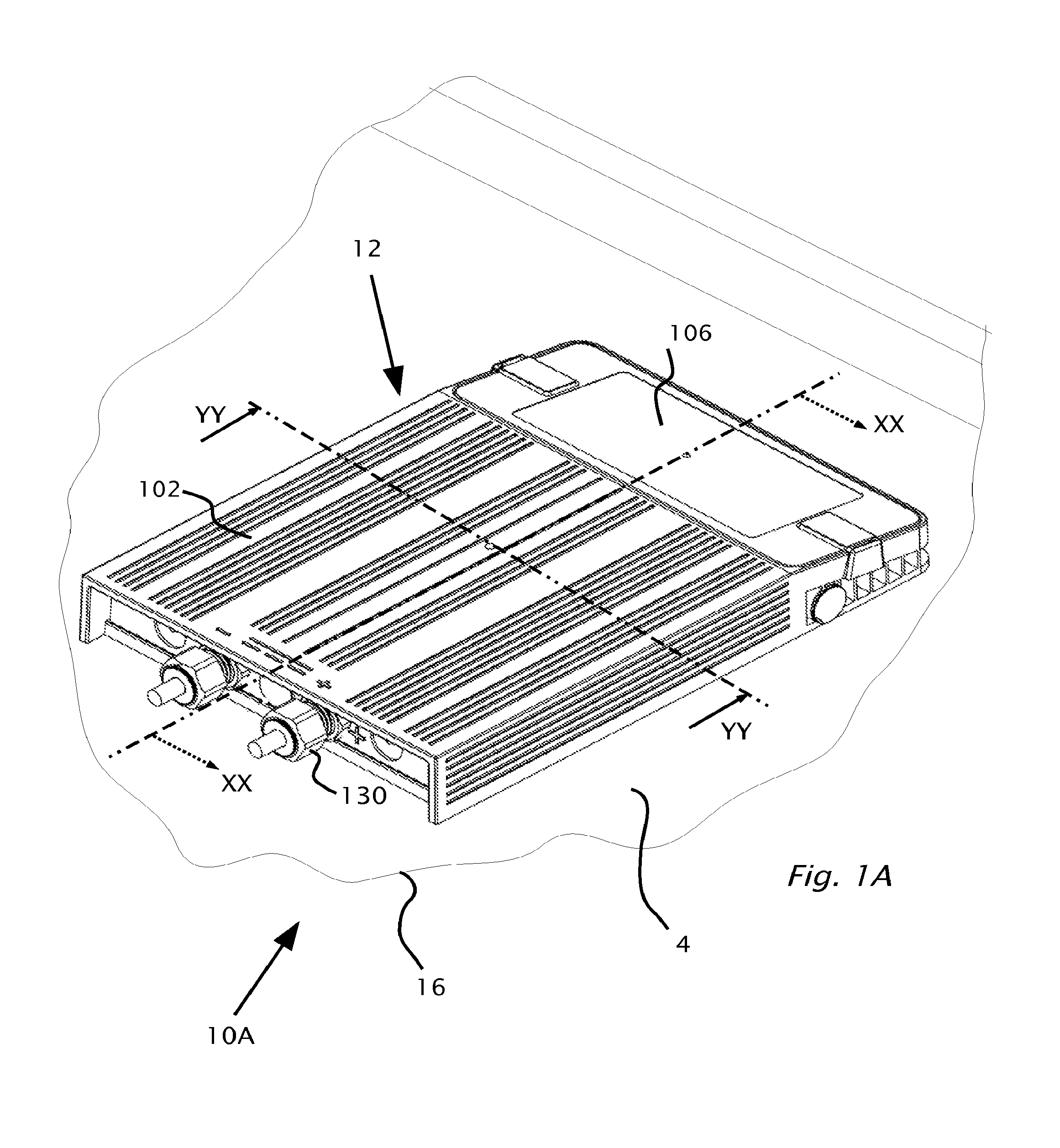
Referring now to the drawings, FIG. 1A shows an isometric view 10A of a junction box 12, according to an embodiment of the present invention. Junction box 12 is shown mounted on the back (or non-photovoltaic side) 4 of a photovoltaic panel 16. Junction box 12 has cable glands 130 which allow for termination of cables inside of junction box 12. Junction box 12 has an outer casing 102 and an access into junction box 12 using a lid 106.
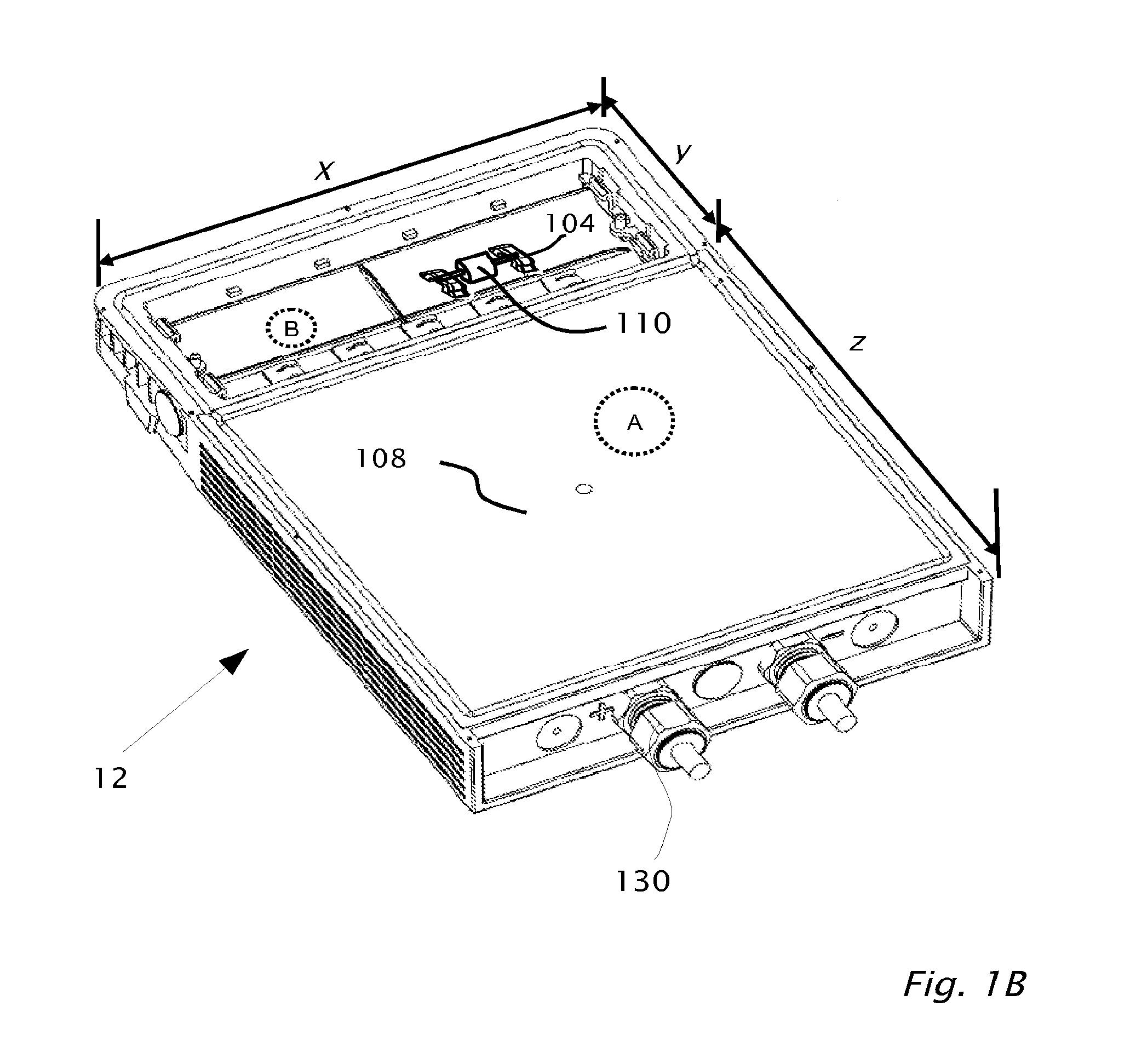
FIG. 1B shows an isometric view of the underside of junction box 12 detached from photovoltaic panel 16. The isometric view shows glands 130 and two sections A and B of junction box 12. chamber A is bounded by the dimensions Z.times.X with chamber A covered by lid 108. Lid 108 gives access into chamber A of junction box 12. Chamber B is an open section which is bounded by dimensions X.times.Y and shows terminals 104. A bypass diode 110 is connected between terminals 104. According to a feature of the present invention, lid 106 removed to access chamber B and lid 108 used to access chamber A are on opposite sides of junction box 12.
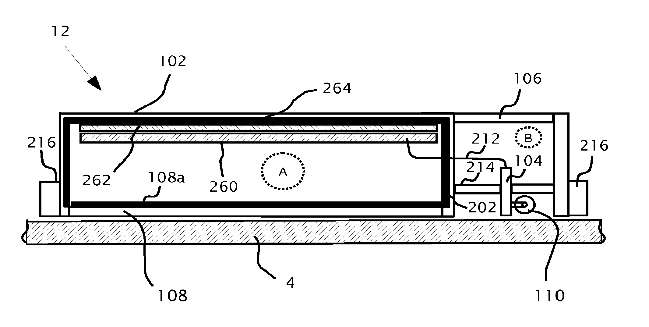
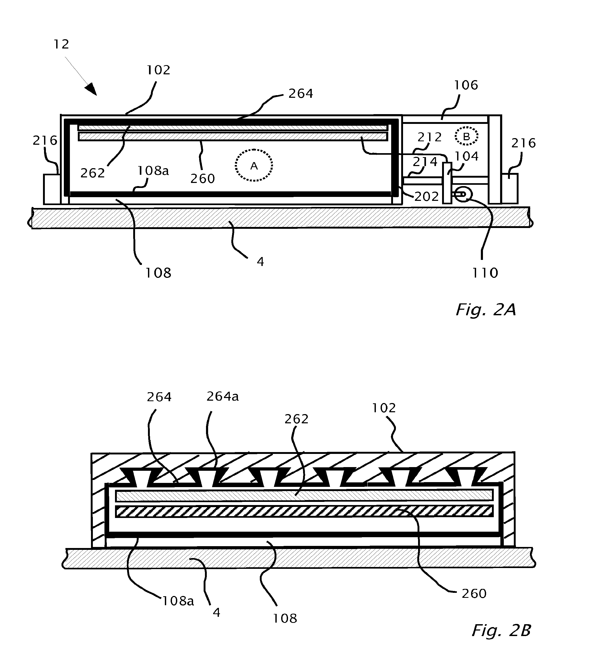
FIG. 2A shows details of cross section XX of junction box 12 indicated by dotted line in FIG. 1A, showing features of the present invention. Cross section XX shows chamber sections A and B of junction box 12 mounted on non-photovoltaic side 4 of photovoltaic panel 16 with clips 216. The mechanical attachment between junction box 12 and photovoltaic panel 16 using clips 216 is such that junction box 12 is flat on photovoltaic panel 16 and a gasket may be used to seal the open end of chamber B.
Chamber A includes circuit board 260, thermally conductive pad 262, heat sink 264, outer casing 102 and lid 108. Circuit board 260 is preferably mounted on supports adapted to receive circuit board 260. Thermal pad 262 provides electrical isolation and thermal conductivity between heat sink 264 and circuit board 260. The component side of circuit board 260 is preferably in contact with thermal pad 262 so that heat created by the components of circuit board 260 is dissipated by heat sink 264 via thermal pad 262. Radio Frequency Interference (RFI) emission from junction box 12 as a result of the operation of circuit board 260 is reduced by having the side of lid 108 coated in an electrically conductive shielding 108a. Shielding 108a connects electrically to heat sink 264 to form a Faraday cage which suppresses RFI emission from junction box 12.
Lid 108 according to an aspect of the present invention is preferably manufactured by an injection molding process. During the injection molding process of lid 207 a shield 108a may be placed in situ and bonded to lid 108 during the injection molding process. Thus, when lid 108 is attached to box chamber A; junction box 12 is electrically isolated by heat sink 264 and shield 108a. Outer casing 102 and lid 108 additionally provide a non-electrically conductive isolation of heat sink 264 and shield 108a between the backside 4 of panel 16 and the exterior of junction box 12. Lid 108 is optionally permanently and/or hermetically sealed to chamber A.
Chamber B includes terminal 104, support 214, bypass diode 110, lid 106, bus bar 212 and wall 202. Wall 202 provides physical separation between chambers A and B. Electrical connectivity between circuit board 260 in chamber A and electrical connector 104 in chamber B is via bus bar 212. Bus bar 212 is sealed in wall 202 in such a way as to preserve the desired hermeticity of chamber A for example against the ingress of water or humidity. Both electrical connector 104 and bus bar 212 are supported mechanically by support 214. Support 214 may also provide hermetic sealing and/or electrical isolation between one end of connector 104 which connects to bus bar 212 and the other end of connector 104 which connects to connections provided by photovoltaic panel 16. Bypass diode 110 connected to connector 104 may be located between support 214 or backside 4 of panel 16 or between support 214 and lid 106. Lid 106 gives access to chamber B whilst junction box 12 is physically attached photovoltaic panel 16 but electrically isolated from panel 16. A preferred mechanism of attaching lid 106 to junction box 12 is to use a rubber gasket arrangement such that chamber B is hermetically sealed against for example the ingress of water/humidity through lid 106 into chamber B.
According to another embodiment of the present invention, junction box 12 is constructed with a wall 202 that may be a double wall so that chamber A and chamber B are mutually separable and re-attachable. Similarly, bus bar 212 is re-connectable between chamber A and chamber B. In this embodiment, a failure within the electronics of circuit board 260 may be repaired by replacing chamber A with a new circuit board 260 without requiring disconnection of chamber B from photovoltaic panel 16. Similarly, an electronics upgrade may be easily achieved.
Junction box 12 including casing 102, lids 108/106, heat sink 264, and thermal pad 262 are preferably adapted to comply with temperature and insulation standard of IEC 61215 (Ed. 2) or other applicable industry standards for use with connection to photovoltaic panels. Junction box 12 and lids 108/106 may be manufactured by injection molding of acrylonitrile butadiene styrene (ABS) thermoplastic, Polybutylene terephthalate (PBT), Poly(p-phenylene oxide) (PPO) or a thermoset such as epoxy resin.
FIG. 2B shows details of cross section YY of junction box 12 indicated by dotted line in FIG. 1A, according to an embodiment of the present invention. Cross section YY is of chamber A mounted on backside 4 of photovoltaic panel 16. Cross section YY shows outer casing 102, heat sink 264 with dovetail structure 264a, thermally conductive pad 262, circuit board 260 and lid 108 with electrical shield 108a.
The manufacture of box chamber sections A and B of junction box 12 in a preferred embodiment of the present invention is by an injection molding process. During the injection molding process heat sink 264 with or without dovetail structure 264a is placed inside box chamber A and is bonded in situ to box chamber A as a result of the injection molding process.
Additional strength of the bonding between heat sink 264 and box chamber A may be provided by a dovetail structure 264a which may be an integral part of heat sink 264. A further function of dovetail structure 264a ensures that the bonding between heat sink 264 and chamber A remains intact when for example junction box 12 is subjected to thermal stresses as a result of electronic components operating inside chamber A, high ambient heat and sunlight when junction box 12 attached to a photovoltaic panel. Where a fastener, e.g. screw is used to fasten chamber A to heat sink 264, the lateral dimensions of dovetail structure 264a is typically increased in order to accommodate the size of the fastener. A further feature of dovetail structure 264a is a hollow structure within dovetail structure 264a which allows for a deformation of dovetail structure 264a. The deformation of dovetail structure 264a allows for the different rates of thermal expansion of enclosure 102 and heat sink 264/dovetail structure 264a during the curing/cooling of the bond between heat sink 264 and enclosure 102 of chamber A.
Reference is now made to FIGS. 3A and 3B which show isometric views of heat sink 264 according to another embodiment of the present invention. Heat sink 264 has four holes 302. Holes 302 are used to attach heat sink 264 into chamber A of junction box 12 using screws. The attachment of heat sink to chamber A may come as an additional step after the injection molding of junction box 12 or of a junction box 12 which is not injection molded. An additional thermal pad may be placed between heat sink 264 and enclosure 102 to ensure good contact between heat sink 264 and enclosure 102 after heat sink 264 is attached enclosure 102. The deformable nature of the thermal pad used to accommodate non-uniformity in surfaces of the heat sink 264 and enclosure 102 due to manufacturing tolerances of heat sink 264/enclosure 102. Alternatively a thermally conducting glue or potting material may be placed between heat sink 264 and enclosure 102.
The articles "a" "an" as used herein mean "one or more" such as "a heat-sink", "a circuit board" have the meaning of "one or more" that is "one or more heat-sinks" or "one or more circuit boards".
Although selected embodiments of the present invention have been shown and described, it is to be understood the present invention is not limited to the described embodiments. Instead, it is to be appreciated that changes may be made to these embodiments without departing from the principles and spirit of the invention, the scope of which is defined by the claims and the equivalents thereof.
* * * * *
D00000
D00001
D00002
D00003
D00004
XML
uspto.report is an independent third-party trademark research tool that is not affiliated, endorsed, or sponsored by the United States Patent and Trademark Office (USPTO) or any other governmental organization. The information provided by uspto.report is based on publicly available data at the time of writing and is intended for informational purposes only.
While we strive to provide accurate and up-to-date information, we do not guarantee the accuracy, completeness, reliability, or suitability of the information displayed on this site. The use of this site is at your own risk. Any reliance you place on such information is therefore strictly at your own risk.
All official trademark data, including owner information, should be verified by visiting the official USPTO website at www.uspto.gov. This site is not intended to replace professional legal advice and should not be used as a substitute for consulting with a legal professional who is knowledgeable about trademark law.