System-on-chip (SoC) optimization through transformation and generation of a network-on-chip (NoC) topology
Rao , et al. July 9, 2
U.S. patent number 10,348,563 [Application Number 15/944,653] was granted by the patent office on 2019-07-09 for system-on-chip (soc) optimization through transformation and generation of a network-on-chip (noc) topology. The grantee listed for this patent is NetSpeed Systems, Inc.. Invention is credited to Sailesh Kumar, Nishant Rao, Pier Giorgio Raponi.


View All Diagrams
| United States Patent | 10,348,563 |
| Rao , et al. | July 9, 2019 |
System-on-chip (SoC) optimization through transformation and generation of a network-on-chip (NoC) topology
Abstract
The present disclosure is directed to system-on-chip (SoC) optimization through transformation and generation of a network-on-chip (NoC) topology. The present disclosure enables transformation from physical placement to logical placement to satisfy bandwidth requirements while maintaining lowest area and lowest routing with minimum cost (wiring and buffering) and latency. In an aspect, method according to the present application includes the steps of receiving at least a floor plan description of an System-on-Chips (SoCs), transforming said floor plan description into at least one logical grid layout of one or more rows and one or more columns, optimizing a number of said one or more rows and said one or more columns based at least on any or combination of a power, an area, or a performance to obtain an optimized transformed logical grid layout, and generating said Network-on-Chip (NoC) topology at least from said optimized transformed logical grid layout.
| Inventors: | Rao; Nishant (San Jose, CA), Kumar; Sailesh (San Jose, CA), Raponi; Pier Giorgio (San Jose, CA) | ||||||||||
|---|---|---|---|---|---|---|---|---|---|---|---|
| Applicant: |
|
||||||||||
| Family ID: | 63038098 | ||||||||||
| Appl. No.: | 15/944,653 | ||||||||||
| Filed: | April 3, 2018 |
Prior Publication Data
| Document Identifier | Publication Date | |
|---|---|---|
| US 20180227180 A1 | Aug 9, 2018 | |
Related U.S. Patent Documents
| Application Number | Filing Date | Patent Number | Issue Date | ||
|---|---|---|---|---|---|
| 14625132 | Feb 18, 2015 | 10050843 | |||
| 62634015 | Feb 22, 2018 | ||||
| Current U.S. Class: | 1/1 |
| Current CPC Class: | G06F 15/76 (20130101); H04L 41/0826 (20130101); G06F 15/7825 (20130101); G06F 30/39 (20200101); G06F 30/392 (20200101); H04L 41/12 (20130101); Y02D 10/14 (20180101); G06F 2119/06 (20200101); Y02D 10/00 (20180101); G06F 2213/0038 (20130101) |
| Current International Class: | H04L 12/24 (20060101); G06F 15/78 (20060101); G06F 17/50 (20060101); G06F 15/76 (20060101) |
References Cited [Referenced By]
U.S. Patent Documents
| 4409838 | October 1983 | Schomberg |
| 4933933 | June 1990 | Dally et al. |
| 5105424 | April 1992 | Flaig et al. |
| 5163016 | November 1992 | Har'El et al. |
| 5355455 | October 1994 | Hilgendorf et al. |
| 5432785 | July 1995 | Ahmed et al. |
| 5563003 | October 1996 | Suzuki et al. |
| 5583990 | December 1996 | Birrittella et al. |
| 5588152 | December 1996 | Dapp et al. |
| 5764740 | June 1998 | Holender |
| 5790554 | August 1998 | Pitcher et al. |
| 5859981 | January 1999 | Levin et al. |
| 5991308 | November 1999 | Fuhrmann et al. |
| 5999530 | December 1999 | LeMaire et al. |
| 6003029 | December 1999 | Agrawal et al. |
| 6029220 | February 2000 | Iwamura et al. |
| 6058385 | May 2000 | Koza et al. |
| 6101181 | August 2000 | Passint et al. |
| 6108739 | August 2000 | James et al. |
| 6249902 | June 2001 | Igusa et al. |
| 6314487 | November 2001 | Hahn et al. |
| 6377543 | April 2002 | Grover et al. |
| 6415282 | July 2002 | Mukherjea et al. |
| 6674720 | January 2004 | Passint et al. |
| 6701361 | March 2004 | Meier |
| 6711717 | March 2004 | Nystrom et al. |
| 6778531 | August 2004 | Kodialam et al. |
| 6925627 | August 2005 | Longway et al. |
| 6967926 | November 2005 | Williams, Jr. et al. |
| 6983461 | January 2006 | Hutchison et al. |
| 7046633 | May 2006 | Carvey |
| 7065730 | June 2006 | Alpert et al. |
| 7143221 | November 2006 | Bruce et al. |
| 7318214 | January 2008 | Prasad et al. |
| 7379424 | May 2008 | Krueger |
| 7437518 | October 2008 | Tsien |
| 7444424 | October 2008 | Tourancheau |
| 7461236 | December 2008 | Wentzlaff |
| 7509619 | March 2009 | Miller et al. |
| 7564865 | July 2009 | Radulescu |
| 7583602 | September 2009 | Bejerano et al. |
| 7590959 | September 2009 | Tanaka |
| 7693064 | April 2010 | Thubert et al. |
| 7701252 | April 2010 | Chow et al. |
| 7724735 | May 2010 | Locatelli et al. |
| 7725859 | May 2010 | Lenahan et al. |
| 7774783 | August 2010 | Toader |
| 7808968 | October 2010 | Kalmanek, Jr. et al. |
| 7830905 | November 2010 | Scott |
| 7853774 | December 2010 | Wentzlaff |
| 7917885 | March 2011 | Becker |
| 7957381 | June 2011 | Clermidy et al. |
| 7973804 | July 2011 | Mejdrich et al. |
| 8018249 | September 2011 | Koch et al. |
| 8020163 | September 2011 | Nollet et al. |
| 8020168 | September 2011 | Hoover et al. |
| 8050256 | November 2011 | Bao et al. |
| 8059551 | November 2011 | Milliken |
| 8098677 | January 2012 | Pleshek et al. |
| 8099757 | January 2012 | Riedle et al. |
| 8136071 | March 2012 | Solomon |
| 8203938 | June 2012 | Gibbings |
| 8261025 | September 2012 | Mejdrich et al. |
| 8281297 | October 2012 | Dasu et al. |
| 8306042 | November 2012 | Abts |
| 8312402 | November 2012 | Okhmatovski et al. |
| 8352774 | January 2013 | Elrabaa |
| 8407425 | March 2013 | Gueron et al. |
| 8412795 | April 2013 | Mangano et al. |
| 8427980 | April 2013 | McLaren |
| 8438578 | May 2013 | Hoover et al. |
| 8448102 | May 2013 | Kornachuk et al. |
| 8490110 | July 2013 | Hoover et al. |
| 8492886 | July 2013 | Or-Bach et al. |
| 8503445 | August 2013 | Lo |
| 8514889 | August 2013 | Jayasimha |
| 8541819 | September 2013 | Or-Bach et al. |
| 8543964 | September 2013 | Ge et al. |
| 8572353 | October 2013 | Bratt et al. |
| 8601423 | December 2013 | Philip et al. |
| 8614955 | December 2013 | Gintis et al. |
| 8619622 | December 2013 | Harrand et al. |
| 8635577 | January 2014 | Kazda et al. |
| 8661455 | February 2014 | Mejdrich et al. |
| 8667439 | March 2014 | Kumar et al. |
| 8705368 | April 2014 | Abts et al. |
| 8711867 | April 2014 | Guo et al. |
| 8717875 | May 2014 | Bejerano et al. |
| 8726295 | May 2014 | Hoover et al. |
| 8738860 | May 2014 | Griffin et al. |
| 8793644 | July 2014 | Michel et al. |
| 8798038 | August 2014 | Jayasimha et al. |
| 8819611 | August 2014 | Philip et al. |
| 8819616 | August 2014 | Philip |
| 8885510 | November 2014 | Kumar et al. |
| 9185023 | November 2015 | Norige |
| 9210048 | December 2015 | Marr et al. |
| 9223711 | December 2015 | Philip et al. |
| 9244845 | January 2016 | Rowlands et al. |
| 9244880 | January 2016 | Philip et al. |
| 9253085 | February 2016 | Kumar et al. |
| 9294354 | March 2016 | Kumar |
| 9294419 | March 2016 | Hasenplaugh |
| 9319232 | April 2016 | Kumar |
| 9444702 | September 2016 | Raponi et al. |
| 9471726 | October 2016 | Kumar et al. |
| 9473359 | October 2016 | Kumar et al. |
| 9473388 | October 2016 | Kumar et al. |
| 9473415 | October 2016 | Kumar |
| 9477280 | October 2016 | Gangwar et al. |
| 9529400 | December 2016 | Kumar et al. |
| 9535848 | January 2017 | Rowlands et al. |
| 9568970 | February 2017 | Kaushal et al. |
| 9569579 | February 2017 | Kumar |
| 9571341 | February 2017 | Kumar et al. |
| 9571402 | February 2017 | Kumar et al. |
| 9571420 | February 2017 | Kumar |
| 9590813 | March 2017 | Kumar et al. |
| 9660942 | May 2017 | Kumar |
| 9699079 | July 2017 | Chopra et al. |
| 9703707 | July 2017 | Falsafi |
| 9742630 | August 2017 | Philip et al. |
| 2002/0071392 | June 2002 | Grover et al. |
| 2002/0073380 | June 2002 | Cooke et al. |
| 2002/0083159 | June 2002 | Ward et al. |
| 2002/0095430 | July 2002 | Egilsson et al. |
| 2002/0150094 | October 2002 | Cheng et al. |
| 2003/0005149 | January 2003 | Haas et al. |
| 2003/0088602 | May 2003 | Dutta et al. |
| 2003/0145314 | July 2003 | Nguyen et al. |
| 2003/0200315 | October 2003 | Goldenberg et al. |
| 2004/0006584 | January 2004 | Vandeweerd |
| 2004/0019814 | January 2004 | Pappalardo et al. |
| 2004/0049565 | March 2004 | Keller et al. |
| 2004/0103218 | May 2004 | Blumrich et al. |
| 2004/0156376 | August 2004 | Nakagawa |
| 2004/0156383 | August 2004 | Nakagawa et al. |
| 2004/0216072 | October 2004 | Alpert et al. |
| 2005/0147081 | July 2005 | Acharya et al. |
| 2005/0203988 | September 2005 | Nollet et al. |
| 2005/0228930 | October 2005 | Ning et al. |
| 2005/0286543 | December 2005 | Coppola et al. |
| 2006/0002303 | January 2006 | Bejerano et al. |
| 2006/0031615 | February 2006 | Bruce et al. |
| 2006/0053312 | March 2006 | Jones et al. |
| 2006/0075169 | April 2006 | Harris et al. |
| 2006/0104274 | May 2006 | Caviglia et al. |
| 2006/0161875 | July 2006 | Rhee |
| 2006/0206297 | September 2006 | Ishiyama et al. |
| 2006/0209846 | September 2006 | Clermidy et al. |
| 2006/0268909 | November 2006 | Langevin et al. |
| 2007/0038987 | February 2007 | Ohara et al. |
| 2007/0088537 | April 2007 | Lertora et al. |
| 2007/0118320 | May 2007 | Luo et al. |
| 2007/0147379 | June 2007 | Lee et al. |
| 2007/0162903 | July 2007 | Babb, II et al. |
| 2007/0189283 | August 2007 | Agarwal et al. |
| 2007/0244676 | October 2007 | Shang et al. |
| 2007/0256044 | November 2007 | Coryer et al. |
| 2007/0267680 | November 2007 | Uchino et al. |
| 2007/0274331 | November 2007 | Locatelli et al. |
| 2008/0072182 | March 2008 | He et al. |
| 2008/0120129 | May 2008 | Seubert et al. |
| 2008/0126569 | May 2008 | Rhim et al. |
| 2008/0127014 | May 2008 | Pandey et al. |
| 2008/0184259 | July 2008 | Lesartre et al. |
| 2008/0186998 | August 2008 | Rijpkema |
| 2008/0211538 | September 2008 | Lajolo et al. |
| 2008/0232387 | September 2008 | Rijpkema et al. |
| 2009/0037888 | February 2009 | Tatsuoka et al. |
| 2009/0046727 | February 2009 | Towles |
| 2009/0067331 | March 2009 | Watsen et al. |
| 2009/0067348 | March 2009 | Vasseur et al. |
| 2009/0070726 | March 2009 | Mehrotra et al. |
| 2009/0083263 | March 2009 | Felch et al. |
| 2009/0089725 | April 2009 | Khan |
| 2009/0109996 | April 2009 | Hoover et al. |
| 2009/0122703 | May 2009 | Gangwal et al. |
| 2009/0125574 | May 2009 | Mejdrich et al. |
| 2009/0125703 | May 2009 | Mejdrich et al. |
| 2009/0125706 | May 2009 | Hoover et al. |
| 2009/0135739 | May 2009 | Hoover et al. |
| 2009/0138567 | May 2009 | Hoover et al. |
| 2009/0150647 | June 2009 | Mejdrich et al. |
| 2009/0157976 | June 2009 | Comparan et al. |
| 2009/0172304 | July 2009 | Gueron et al. |
| 2009/0182944 | July 2009 | Comparan et al. |
| 2009/0182954 | July 2009 | Mejdrich et al. |
| 2009/0182986 | July 2009 | Schwinn et al. |
| 2009/0182987 | July 2009 | Mejdrich et al. |
| 2009/0187716 | July 2009 | Comparan et al. |
| 2009/0187734 | July 2009 | Mejdrich et al. |
| 2009/0187756 | July 2009 | Nollet et al. |
| 2009/0201302 | August 2009 | Hoover et al. |
| 2009/0210184 | August 2009 | Medardoni et al. |
| 2009/0210883 | August 2009 | Hoover et al. |
| 2009/0228681 | September 2009 | Mejdrich et al. |
| 2009/0228682 | September 2009 | Mejdrich et al. |
| 2009/0228689 | September 2009 | Muff et al. |
| 2009/0228690 | September 2009 | Muff et al. |
| 2009/0231348 | September 2009 | Mejdrich et al. |
| 2009/0231349 | September 2009 | Mejdrich et al. |
| 2009/0240920 | September 2009 | Muff et al. |
| 2009/0245257 | October 2009 | Comparan et al. |
| 2009/0256836 | October 2009 | Fowler et al. |
| 2009/0260013 | October 2009 | Heil et al. |
| 2009/0268677 | October 2009 | Chou et al. |
| 2009/0271172 | October 2009 | Mejdrich et al. |
| 2009/0276572 | November 2009 | Heil et al. |
| 2009/0282139 | November 2009 | Mejdrich et al. |
| 2009/0282197 | November 2009 | Comparan et al. |
| 2009/0282211 | November 2009 | Hoover et al. |
| 2009/0282214 | November 2009 | Kuesel et al. |
| 2009/0282221 | November 2009 | Heil et al. |
| 2009/0282222 | November 2009 | Hoover et al. |
| 2009/0282226 | November 2009 | Hoover et al. |
| 2009/0282227 | November 2009 | Hoover et al. |
| 2009/0282419 | November 2009 | Mejdrich et al. |
| 2009/0285222 | November 2009 | Hoover et al. |
| 2009/0287885 | November 2009 | Kriegel et al. |
| 2009/0292907 | November 2009 | Schwinn et al. |
| 2009/0293061 | November 2009 | Schwinn et al. |
| 2009/0300292 | December 2009 | Fang et al. |
| 2009/0300335 | December 2009 | Muff et al. |
| 2009/0307714 | December 2009 | Hoover et al. |
| 2009/0313592 | December 2009 | Murali et al. |
| 2009/0315908 | December 2009 | Comparan et al. |
| 2010/0023568 | January 2010 | Hickey et al. |
| 2010/0031009 | February 2010 | Muff et al. |
| 2010/0040162 | February 2010 | Suehiro |
| 2010/0042812 | February 2010 | Hickey et al. |
| 2010/0042813 | February 2010 | Hickey et al. |
| 2010/0070714 | March 2010 | Hoover et al. |
| 2010/0091787 | April 2010 | Muff et al. |
| 2010/0100707 | April 2010 | Mejdrich et al. |
| 2010/0100712 | April 2010 | Mejdrich et al. |
| 2010/0100770 | April 2010 | Mejdrich et al. |
| 2010/0100934 | April 2010 | Mejdrich et al. |
| 2010/0106940 | April 2010 | Muff et al. |
| 2010/0125722 | May 2010 | Hickey et al. |
| 2010/0158005 | June 2010 | Mukhopadhyay et al. |
| 2010/0162019 | June 2010 | Kumar et al. |
| 2010/0189111 | July 2010 | Muff et al. |
| 2010/0191940 | July 2010 | Mejdrich et al. |
| 2010/0211718 | August 2010 | Gratz et al. |
| 2010/0223505 | September 2010 | Andreev et al. |
| 2010/0228781 | September 2010 | Fowler et al. |
| 2010/0239185 | September 2010 | Fowler et al. |
| 2010/0239186 | September 2010 | Fowler et al. |
| 2010/0242003 | September 2010 | Kwok |
| 2010/0269123 | October 2010 | Mejdrich et al. |
| 2010/0284309 | November 2010 | Allan et al. |
| 2010/0333099 | December 2010 | Kupferschmidt et al. |
| 2011/0022754 | January 2011 | Cidon et al. |
| 2011/0035523 | February 2011 | Feero et al. |
| 2011/0044336 | February 2011 | Umeshima |
| 2011/0060831 | March 2011 | Ishii et al. |
| 2011/0063285 | March 2011 | Hoover et al. |
| 2011/0064077 | March 2011 | Wen |
| 2011/0072407 | March 2011 | Keinert et al. |
| 2011/0085550 | April 2011 | Lecler et al. |
| 2011/0085561 | April 2011 | Ahn et al. |
| 2011/0103799 | May 2011 | Shacham et al. |
| 2011/0119322 | May 2011 | Li et al. |
| 2011/0154282 | June 2011 | Chang et al. |
| 2011/0173258 | July 2011 | Arimilli et al. |
| 2011/0191088 | August 2011 | Hsu et al. |
| 2011/0191774 | August 2011 | Hsu et al. |
| 2011/0235531 | September 2011 | Vangal et al. |
| 2011/0243147 | October 2011 | Paul |
| 2011/0276937 | November 2011 | Waller |
| 2011/0289485 | November 2011 | Mejdrich et al. |
| 2011/0292063 | December 2011 | Mejdrich et al. |
| 2011/0302345 | December 2011 | Boucard et al. |
| 2011/0302450 | December 2011 | Hickey et al. |
| 2011/0307734 | December 2011 | Boesen et al. |
| 2011/0316864 | December 2011 | Mejdrich et al. |
| 2011/0320719 | December 2011 | Mejdrich et al. |
| 2011/0320724 | December 2011 | Mejdrich et al. |
| 2011/0320771 | December 2011 | Mejdrich et al. |
| 2011/0320854 | December 2011 | Elrabaa |
| 2011/0320991 | December 2011 | Hsu et al. |
| 2011/0321057 | December 2011 | Mejdrich et al. |
| 2012/0022841 | January 2012 | Appleyard |
| 2012/0023473 | January 2012 | Brown et al. |
| 2012/0026917 | February 2012 | Guo et al. |
| 2012/0054511 | March 2012 | Brinks et al. |
| 2012/0072635 | March 2012 | Yoshida et al. |
| 2012/0079147 | March 2012 | Ishii et al. |
| 2012/0099475 | April 2012 | Tokuoka |
| 2012/0110106 | May 2012 | De Lescure et al. |
| 2012/0110541 | May 2012 | Ge et al. |
| 2012/0144065 | June 2012 | Parker et al. |
| 2012/0155250 | June 2012 | Carney et al. |
| 2012/0173846 | July 2012 | Wang et al. |
| 2012/0176364 | July 2012 | Schardt et al. |
| 2012/0195321 | August 2012 | Ramanujam et al. |
| 2012/0198408 | August 2012 | Chopra |
| 2012/0209944 | August 2012 | Mejdrich et al. |
| 2012/0218998 | August 2012 | Sarikaya |
| 2012/0221711 | August 2012 | Kuesel et al. |
| 2012/0260252 | October 2012 | Kuesel et al. |
| 2012/0311512 | December 2012 | Michel et al. |
| 2013/0021896 | January 2013 | Pu et al. |
| 2013/0028083 | January 2013 | Yoshida et al. |
| 2013/0028090 | January 2013 | Yamaguchi et al. |
| 2013/0028261 | January 2013 | Lee |
| 2013/0036296 | February 2013 | Hickey et al. |
| 2013/0044117 | February 2013 | Mejdrich et al. |
| 2013/0046518 | February 2013 | Mejdrich et al. |
| 2013/0051397 | February 2013 | Guo et al. |
| 2013/0054811 | February 2013 | Harrand |
| 2013/0073771 | March 2013 | Hanyu et al. |
| 2013/0073878 | March 2013 | Jayasimha et al. |
| 2013/0080073 | March 2013 | de Corral |
| 2013/0080671 | March 2013 | Ishii et al. |
| 2013/0086399 | April 2013 | Tychon et al. |
| 2013/0103369 | April 2013 | Huynh et al. |
| 2013/0103912 | April 2013 | Jones et al. |
| 2013/0111190 | May 2013 | Muff et al. |
| 2013/0111242 | May 2013 | Heller et al. |
| 2013/0117543 | May 2013 | Venkataramanan et al. |
| 2013/0138925 | May 2013 | Hickey et al. |
| 2013/0145128 | June 2013 | Schardt et al. |
| 2013/0148506 | June 2013 | Lea |
| 2013/0151215 | June 2013 | Mustapha |
| 2013/0159668 | June 2013 | Muff et al. |
| 2013/0159669 | June 2013 | Comparan et al. |
| 2013/0159674 | June 2013 | Muff et al. |
| 2013/0159675 | June 2013 | Muff et al. |
| 2013/0159676 | June 2013 | Muff et al. |
| 2013/0159944 | June 2013 | Uno et al. |
| 2013/0160026 | June 2013 | Kuesel et al. |
| 2013/0160114 | June 2013 | Greenwood et al. |
| 2013/0163615 | June 2013 | Mangano et al. |
| 2013/0174113 | July 2013 | Lecler et al. |
| 2013/0179613 | July 2013 | Boucard et al. |
| 2013/0179902 | July 2013 | Hoover et al. |
| 2013/0185542 | July 2013 | Mejdrich et al. |
| 2013/0191572 | July 2013 | Nooney et al. |
| 2013/0191600 | July 2013 | Kuesel et al. |
| 2013/0191649 | July 2013 | Muff et al. |
| 2013/0191651 | July 2013 | Muff et al. |
| 2013/0191824 | July 2013 | Muff et al. |
| 2013/0191825 | July 2013 | Muff et al. |
| 2013/0207801 | August 2013 | Barnes |
| 2013/0219148 | August 2013 | Chen et al. |
| 2013/0250792 | September 2013 | Yoshida et al. |
| 2013/0254488 | September 2013 | Kaxiras et al. |
| 2013/0263068 | October 2013 | Cho et al. |
| 2013/0268990 | October 2013 | Urzi et al. |
| 2013/0294458 | November 2013 | Yamaguchi et al. |
| 2013/0305207 | November 2013 | Hsieh et al. |
| 2013/0311819 | November 2013 | Ishii et al. |
| 2013/0326458 | December 2013 | Kazda et al. |
| 2014/0013293 | January 2014 | Hsu et al. |
| 2014/0068132 | March 2014 | Philip et al. |
| 2014/0068134 | March 2014 | Philip et al. |
| 2014/0082237 | March 2014 | Wertheimer et al. |
| 2014/0086260 | March 2014 | Dai et al. |
| 2014/0092740 | April 2014 | Wang et al. |
| 2014/0098683 | April 2014 | Kumar et al. |
| 2014/0112149 | April 2014 | Urzi et al. |
| 2014/0115218 | April 2014 | Philip et al. |
| 2014/0115298 | April 2014 | Philip et al. |
| 2014/0126572 | May 2014 | Hutton et al. |
| 2014/0143557 | May 2014 | Kuesel et al. |
| 2014/0143558 | May 2014 | Kuesel et al. |
| 2014/0149720 | May 2014 | Muff et al. |
| 2014/0164465 | June 2014 | Muff et al. |
| 2014/0164704 | June 2014 | Kuesel et al. |
| 2014/0164732 | June 2014 | Muff et al. |
| 2014/0164734 | June 2014 | Muff et al. |
| 2014/0211622 | July 2014 | Kumar et al. |
| 2014/0229709 | August 2014 | Kuesel et al. |
| 2014/0229712 | August 2014 | Muff et al. |
| 2014/0229713 | August 2014 | Muff et al. |
| 2014/0229714 | August 2014 | Muff et al. |
| 2014/0229720 | August 2014 | Hickey et al. |
| 2014/0230077 | August 2014 | Muff et al. |
| 2014/0232188 | August 2014 | Cheriyan et al. |
| 2014/0241376 | August 2014 | Balkan et al. |
| 2014/0254388 | September 2014 | Kumar et al. |
| 2014/0281243 | September 2014 | Shalf et al. |
| 2014/0281402 | September 2014 | Comparan et al. |
| 2014/0307590 | October 2014 | Dobbelaere et al. |
| 2014/0359641 | December 2014 | Clark et al. |
| 2014/0376569 | December 2014 | Philip et al. |
| 2015/0020078 | January 2015 | Kuesel et al. |
| 2015/0026435 | January 2015 | Muff et al. |
| 2015/0026494 | January 2015 | Bainbridge et al. |
| 2015/0026500 | January 2015 | Muff et al. |
| 2015/0032988 | January 2015 | Muff et al. |
| 2015/0032999 | January 2015 | Muff et al. |
| 2015/0043575 | February 2015 | Kumar et al. |
| 2015/0081941 | March 2015 | Brown et al. |
| 2015/0103822 | April 2015 | Gianchandani et al. |
| 2015/0109024 | April 2015 | Abdelfattah et al. |
| 2015/0159330 | June 2015 | Weisman et al. |
| 2015/0178435 | June 2015 | Kumar |
| 2015/0331831 | November 2015 | Solihin |
| 2015/0348600 | December 2015 | Bhatia et al. |
| 2015/0381707 | December 2015 | How |
| 2017/0061053 | March 2017 | Kumar et al. |
| 2017/0063625 | March 2017 | Philip et al. |
| 2017/0063634 | March 2017 | Norige |
| 2017/0063697 | March 2017 | Kumar |
| 103684961 | Mar 2014 | CN | |||
| 5936793 | May 2016 | JP | |||
| 6060316 | Jan 2017 | JP | |||
| 6093867 | Feb 2017 | JP | |||
| 10-2013-0033898 | Apr 2013 | KR | |||
| 101652490 | Aug 2016 | KR | |||
| 101707655 | Feb 2017 | KR | |||
| 2010074872 | Jul 2010 | WO | |||
| 2013063484 | May 2013 | WO | |||
| 2014059024 | Apr 2014 | WO | |||
Other References
|
Ababei, C., et al., Achieving Network on Chip Fault Tolerance by Adaptive Remapping, Parallel & Distributed Processing, 2009, IEEE International Symposium, 4 pgs. cited by applicant . Abts, D., et al., Age-Based Packet Arbitration in Large-Radix k-ary n-cubes, Supercomputing 2007 (SC07), Nov. 10-16, 2007, 11 pgs. cited by applicant . Beretta, I, et al., A Mapping Flow for Dynamically Reconfigurable Multi-Core System-on-Chip Design, IEEE Transactions on Computer-Aided Design of Integrated Circuits and Systems, Aug. 2011, 30(8), pp. 1211-1224. cited by applicant . Das, R., et al., Aergia: Exploiting Packet Latency Slack in On-Chip Networks, 37th International Symposium on Computer Architecture (ISCA '10), Jun. 19-23, 2010, 11 pgs. cited by applicant . Ebrahimi, E., et al., Fairness via Source Throttling: A Configurable and High-Performance Fairness Substrate for Multi-Core Memory Systems, ASPLOS '10, Mar. 13-17, 2010, 12 pgs. cited by applicant . Gindin, R., et al., NoC-Based FPGA: Architecture and Routing, Proceedings of the First International Symposium on Networks-on-Chip (NOCS'07), May 2007, pp. 253-262. cited by applicant . Grot, B., Preemptive Virtual Clock: A Flexible, Efficient, and Cost-Effective QOS Scheme for Networks-on-Chip, Micro '09, Dec. 16, 2009, 12 pgs. cited by applicant . Grot, B., Kilo-NOC: A Heterogeneous Network-on-Chip Architecture for Scalability and Service Guarantees, ISCA 11, Jun. 4-8, 2011, 12 pgs. cited by applicant . Grot, B., Topology-Aware Quality-of-Service Support in Highly Integrated Chip Multiprocessors, 6th Annual Workshop on the Interaction between Operating Systems and Computer Architecture, Jun. 2006, 11 pgs. cited by applicant . Hestness, J., et al., Netrace: Dependency-Tracking for Efficient Network-on-Chip Experimentation, The University of Texas at Austin, Dept. of Computer Science, May 2011, 20 pgs. cited by applicant . Jiang, N., et al., Performance Implications of Age-Based Allocations in On-Chip Networks, CVA Memo 129, May 24, 2011, 21 pgs. cited by applicant . Lee, J. W., et al., Globally-Synchronized Frames for Guaranteed Quality-of-Service in On-Chip Networks, 35th IEEE/ACM International Symposium on Computer Architecture (ISCA), Jun. 2008, 12 pgs. cited by applicant . Lee, M. M., et al., Approximating Age-Based Arbitration in On-Chip Networks, PACT '10, Sep. 11-15, 2010, 2 pgs. cited by applicant . Li, B., et al., CoQoS: Coordinating QoS-Aware Shared Resources in NoC-based SoCs, J. Parallel Distrib. Comput., 71(5), May 2011, 14 pgs. cited by applicant . Lin, S., et al., Scalable Connection-Based Flow Control Scheme for Application-Specific Network-on-Chip, The Journal of China Universities of Posts and Telecommunications, Dec. 2011, 18(6), pp. 98-105. cited by applicant . Bolotin, Evgency, et al., "QNoC: QoS Architecture and Design Process for Network on Chip" 2004, 24 pages, Journal of Systems Architecture 50 (2004) 105-128 Elsevier. cited by applicant . Holsmark, Shashi Kumar Rickard, et al., "HiRA: A Methodology for Deadlock Free Routing in Hierarchical Networks on Chip", 10 pages, (978-1-4244-4143-3/09 2009 IEEE). cited by applicant . Munirul, H.M., et al., Evaluation of Multiple-Valued Packet Multiplexing Scheme for Network-on-Chip Architecture, Proceedings of the 36th International Symposium on Multiple-Valued Logic (ISMVL '06), 2006, 6 pgs. cited by applicant . Rajesh BV, Shivaputra, "NOC: Design and Implementation of Hardware Network Interface With Improved Communication Reliability", 7 pages, International Journal of VLSI and Embedded Systems, IJIVES (vol. 04, Article 06116; Jun. 2013). cited by applicant . Yang, J., et al., Homogeneous NoC-based FPGA: The Foundation for Virtual FPGA, 10th IEEE International Conference on Computer and Information Technology (CIT 2010), Jun. 2010, pp. 62-67. cited by applicant . Zaman, Aanam, "Formal Verification of Circuit-Switched Network on Chip (NoC) Architectures using SPIN", Oosman Hasan, IEEE .COPYRGT. 2014, 8 pages. cited by applicant . Benini, Luca, et al., "Networks on Chips: A New SoC Paradigm", IEEE Computers, SOC Designs, pp. 70-78, Copyright 2002 IEEE. 0018-9162/02. cited by applicant . Sethuraman, Ranga Vemuri Balasubramanian, "optiMap: A Tool for Automated Generation of NoC Architecture Using Multi-Port Routers for FPGAs", IEEE, pp. 1-6, 2006. cited by applicant . International Search Report and Written Opinion for PCT/US2014/060745, dated Jan. 21, 2015, 10 pgs. cited by applicant . International Search Report and Written Opinion for PCT/US2014/060879, dated Jan. 21, 2015, 10 pgs. cited by applicant . International Search Report and Written Opinion for PCT/US2014/060892, dated Jan. 27, 2015, 10 pgs. cited by applicant . International Search Report and Written Opinion for PCT/US2014/060886, dated Jan. 26, 2015, 10 pgs. cited by applicant . International Search Report and Written Opinion for PCT/US2013/064140, dated Jan. 22, 2014, 9 pgs. cited by applicant . International Search Report and Written Opinion for PCT/US2014/012003, dated Mar. 26, 2014, 9 pgs. cited by applicant . International Search Report and Written Opinion for PCT/US2014/012012, dated May 14, 2014, 9 pgs. cited by applicant . International Search Report and Written Opinion for PCT/US2014/023625, dated Jul. 10, 2014, 9 pgs. cited by applicant . International Preliminary Report on Patentability for International Application No. PCT/US2013/064140, dated Apr. 14, 2015, 5 pages. cited by applicant . Office Action for Korean Patent Application No. 10-2016-7019093 dated Sep. 8, 2016, 3 pages plus 1 page English translation. KIPO, Korea. cited by applicant . Notice of Allowance for for Korean Patent Application No. 10-2016-7019093 dated Sep. 8, 2016, 4 pages. KIPO, Korea. cited by applicant . International Search Report and Written Opinion for PCT/US2014/037902, dated Sep. 30, 2014, 14 pgs. cited by applicant . Office Action for Japanese Patent Application No. 2015-535898 dated Oct. 25, 2016, 2 pages English, 2 pages untranslated. Japan Patent Office. cited by applicant . Notice of Grant for Japanese Patent Application No. 2015-535898 dated Jan. 17, 2017, 3 pages, untranslated. Japan Patent Office. cited by applicant . International Search Report and Written Opinion for PCT/US2014/048190, dated Nov. 28, 2014, 11 pgs. cited by applicant . Office Action for Japanese Patent Application No. 2016-516030 dated Aug. 30, 2016, 2 pages, Japan Patent Office. cited by applicant . Decision to Grant for Japanese Patent Application No. 2016-516030 dated Nov. 22, 2016, 6 pages, untranslated, Japan Patent Office. cited by applicant. |
Primary Examiner: Levin; Naum
Attorney, Agent or Firm: Spectrum IP Law Group LLC
Parent Case Text
CROSS REFERENCE TO RELATED APPLICATION
This U.S. patent application is a continuation in part application of U.S. patent application Ser. No. 14/625,132, filed on Feb. 18, 2015, now issued as U.S. Pat. No. 10,050,843, and is also based on and claims the benefit of domestic priority under 35 U.S.C. 119(e) from provisional U.S. patent application No. 62/634,015, filed on Feb. 22, 2018, the disclosures of which is hereby incorporated by reference herein in its entirety.
Claims
What is claimed is:
1. A method for generating a Network-on-Chip (NoC) topology, said method comprising: receiving a floor plan description of a System-on-Chip (SoC); transforming said floor plan description into a logical grid layout comprising one or more rows and one or more columns; optimizing a number of said one or more rows and said one or more columns based at least on one of a power of the NoC, an area of the NoC, and a performance of the NoC to obtain an optimized transformed logical grid layout; and generating said Network-on-Chip (NoC) topology at least from said optimized transformed logical grid layout, wherein said floor plan description comprises router radix information and router arbitration frequency information, the number of said one or more rows and said one or more columns are optimized based on said router radix information and said router arbitration frequency information.
2. The method of claim 1, wherein said floor plan description comprises at least one of one or more positions of at least one host, one or more sizes of SoC, and one or more positions of at least one bridge.
3. The method of claim 1, wherein said one or more rows and said one or more columns are determined at least from one or more corners associated with one or more hosts.
4. The method of claim 1, wherein each intersection of said one or more rows and said one or more columns is indicative of a potential router location.
5. The method of claim 1, further comprising: generating one or more connections on said optimized transformed logical grid layout based at least on overlapping hosts on one or more connection paths or bridges.
6. The method of claim 1, further comprising: removing one or more connections on said optimized transformed logical grid layout based at least on overlapping hosts on one or more connection paths or bridges.
7. The method of claim 1, wherein said one or more rows and said one or more columns are decided based on one or more domains, the one or more domains comprising at least one or more of a clock domain, a power domain, and a domain determined from physical constraints.
8. The method of claim 1, wherein said floor plan description comprises traffic information, wherein the number of said one or more rows and said one or more columns are optimized based on the traffic information.
9. The method of claim 1, wherein said step of optimizing is an iterative process involving tolerance.
10. The method of claim 1, wherein said floor plan description comprises chip size information, wherein the number of said one or more rows and said one or more columns are optimized based on the chip size information, the chip size information comprising information associated with a placement of one or more wires in a gap.
11. The method of claim 1, wherein the optimizing a number of said one or more rows and said one or more columns comprises, determining a width for each of said one or more columns based on the floorplan description of the SoC, wherein a width of a first column of said one or more columns has a different width than a width of a second column of said one or more columns.
12. A non-transitory computer readable medium, storing instructions for generating a Network-on-Chip (NoC) topology, said instructions comprising: receiving a floor plan description of a System-on-Chip (SoC); transforming said floor plan description into a logical grid layout comprising one or more rows and one or more columns; optimizing a number of said one or more rows and said one or more columns based at least on one of a power of the NoC, an area of the NoC, and a performance of the NoC to obtain an optimized transformed logical grid layout; and generating said Network-on-Chip (NoC) topology at least from said optimized transformed logical grid layout; wherein said floor plan description comprises router radix information and router arbitration frequency information, the number of said one or more rows and said one or more columns are optimized based on said router radix information and said router arbitration frequency information.
13. The non-transitory computer readable medium of claim 12, wherein said floor plan description comprises at least one of one or more positions of at least one host, one or more sizes of SoC, and one or more positions of at least one bridge.
14. The non-transitory computer readable medium of claim 12, wherein said one or more rows and said one or more columns are determined at least from one or more corners associated with one or more hosts.
15. The non-transitory computer readable medium of claim 12, wherein each intersection of said one or more rows and said one or more columns is indicative of a potential router location.
16. The non-transitory computer readable medium of claim 12, the instructions further comprising: generating one or more connections on said optimized transformed logical grid layout based at least on overlapping hosts on one or more connection paths or bridges.
17. The non-transitory computer readable medium of claim 12, the instructions further comprising: removing one or more connections on said optimized transformed logical grid layout based at least on overlapping hosts on one or more connection paths or bridges.
18. The non-transitory computer readable medium of claim 12, wherein said one or more rows and said one or more columns are decided based on one or more domains, the one or more domains comprising at least one or more of a clock domain, a power domain, and a domain determined from physical constraints.
Description
TECHNICAL FIELD
Methods and example implementations described herein are generally directed to an interconnect architecture, and more specifically, to system-on-chip (SoC) optimization through transformation and to automatically generate an optimized network-on-chip (NoC) topology for a given user specified physical topological constraints.
RELATED ART
The number of components on a chip is rapidly growing due to increasing levels of integration, system complexity and shrinking transistor geometry. Complex System-on-Chips (SoCs) may involve a variety of components e.g., processor cores, DSPs, hardware accelerators, memory and I/O, while Chip Multi-Processors (CMPs) may involve a large number of homogenous processor cores, memory and I/O subsystems. In both SoC and CMP systems, the on-chip interconnect plays a role in providing high-performance communication between the various components. Due to scalability limitations of traditional buses and crossbar based interconnects, Network-on-Chip (NoC) has emerged as a paradigm to interconnect a large number of components on the chip. NoC is a global shared communication infrastructure made up of several routing nodes interconnected with each other using point-to-point physical links.
Messages are injected by the source and are routed from the source node to the destination over multiple intermediate nodes and physical links. The destination node then ejects the message and provides the message to the destination. For the remainder of this application, the terms `components`, `blocks`, `hosts` or `cores` will be used interchangeably to refer to the various system components which are interconnected using a NoC. Terms `routers` and `nodes` will also be used interchangeably. Without loss of generalization, the system with multiple interconnected components will itself be referred to as a `multi-core system`.
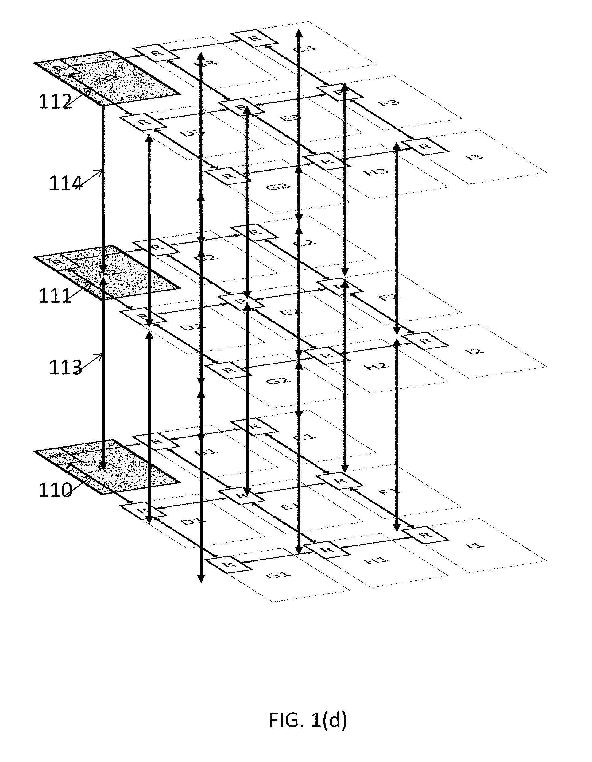
There are several topologies in which the routers can connect to one another to create the system network. Bi-directional rings (as shown in FIG. 1A, 2-D (two dimensional) mesh (as shown in FIG. 1B), and 2-D Taurus (as shown in FIG. 1C) are examples of topologies in the related art. Mesh and Taurus can also be extended to 2.5-D (two and half dimensional) or 3-D (three dimensional) organizations. FIG. 1D shows a 3D mesh NoC, where there are three layers of 3.times.3 2D mesh NoC shown over each other. The NoC routers have up to two additional ports, one connecting to a router in the higher layer, and another connecting to a router in the lower layer. Router 111 in the middle layer of the example has its ports used, one connecting to the router 112 at the top layer and another connecting to the router 110 at the bottom layer. Routers 110 and 112 are at the bottom and top mesh layers respectively and therefore have only the upper facing port 113 and the lower facing port 114 respectively connected.
Packets are message transport units for intercommunication between various components. Routing involves identifying a path that is a set of routers and physical links of the network over which packets are sent from a source to a destination. Components are connected to one or multiple ports of one or multiple routers; with each such port having a unique identification (ID). Packets can carry the destination's router and port ID for use by the intermediate routers to route the packet to the destination component.
Examples of routing techniques include deterministic routing, which involves choosing the same path from A to B for every packet. This form of routing is independent from the state of the network and does not load balance across path diversities, which might exist in the underlying network. However, such deterministic routing may implemented in hardware, maintains packet ordering and may be rendered free of network level deadlocks. Shortest path routing may minimize the latency as such routing reduces the number of hops from the source to the destination. For this reason, the shortest path may also be the lowest power path for communication between the two components. Dimension-order routing is a form of deterministic shortest path routing in 2-D, 2.5-D, and 3-D mesh networks. In this routing scheme, messages are routed along each coordinates in a particular sequence until the message reaches the final destination. For example in a 3-D mesh network, one may first route along the X dimension until it reaches a router whose X-coordinate is equal to the X-coordinate of the destination router. Next, the message takes a turn and is routed in along Y dimension and finally takes another turn and moves along the Z dimension until the message reaches the final destination router. Dimension ordered routing may be minimal turn and shortest path routing.
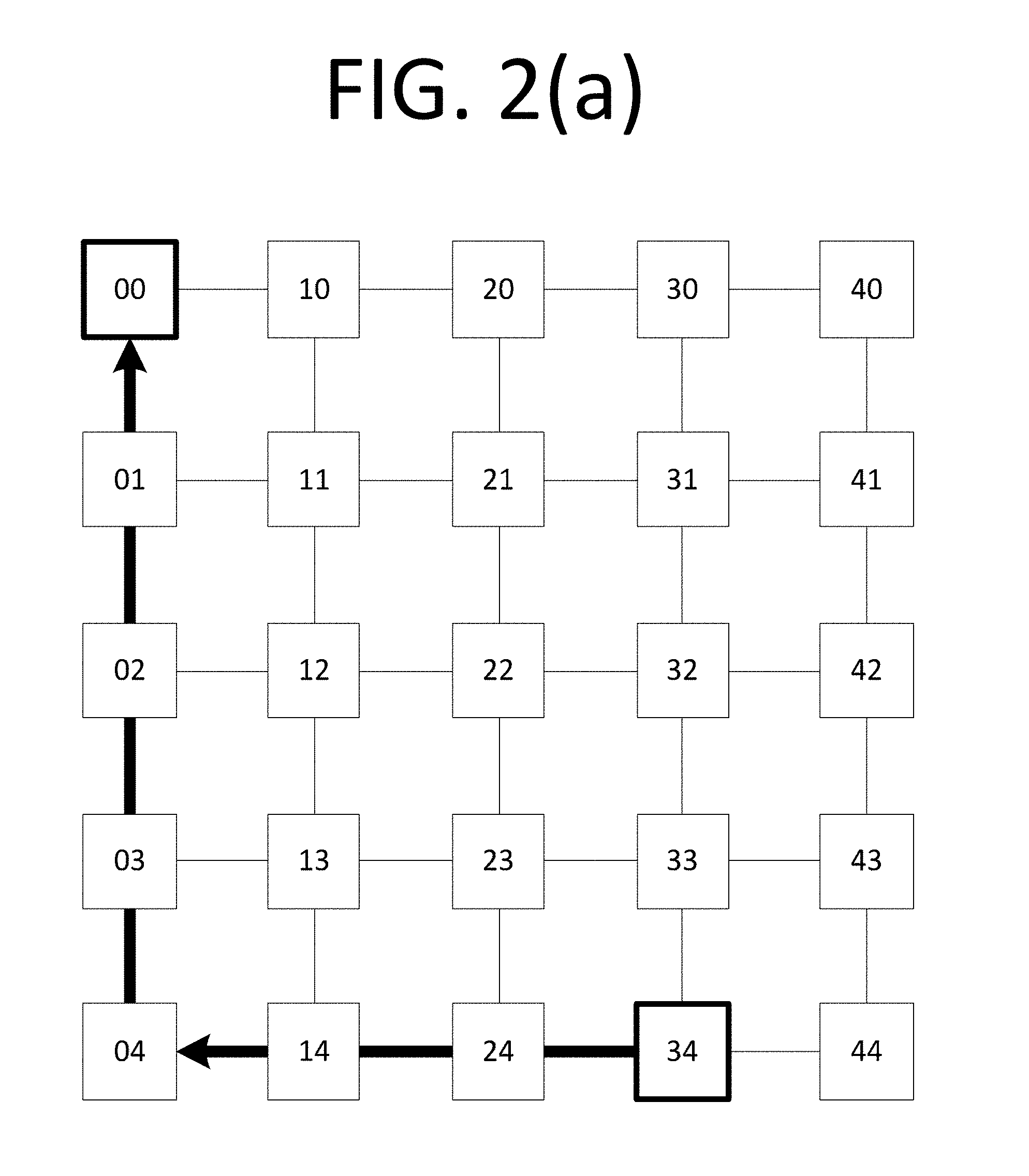
FIG. 2A pictorially illustrates an example of XY routing in a two dimensional mesh. More specifically, FIG. 2A illustrates XY routing from node `34` to node `00`. In the example of FIG. 2A, each component is connected to only one port of one router. A packet is first routed over the X-axis till the packet reaches node `04` where the X-coordinate of the node is the same as the X-coordinate of the destination node. The packet is next routed over the Y-axis until the packet reaches the destination node.
In heterogeneous mesh topology in which one or more routers or one or more links are absent, dimension order routing may not be feasible between certain source and destination nodes, and alternative paths may have to be taken. The alternative paths may not be shortest or minimum turn.
Source routing and routing using tables are other routing options used in NoC. Adaptive routing can dynamically change the path taken between two points on the network based on the state of the network. This form of routing may be complex to analyze and implement.
A NoC interconnect may contain multiple physical networks. Over each physical network, there exist multiple virtual networks, wherein different message types are transmitted over different virtual networks. In this case, at each physical link or channel, there are multiple virtual channels; each virtual channel may have dedicated buffers at both end points. In any given clock cycle, only one virtual channel can transmit data on the physical channel.
NoC interconnects may employ wormhole routing, wherein, a large message or packet is broken into small pieces known as flits (also referred to as flow control digits). The first flit is a header flit, which holds information about this packet's route and key message level info along with payload data and sets up the routing behavior for all subsequent flits associated with the message. Optionally, one or more body flits follows the header flit, containing remaining payload of data. The final flit is a tail flit, which, in addition to containing last payload, also performs some bookkeeping to close the connection for the message. In wormhole flow control, virtual channels are often implemented.
The physical channels are time sliced into a number of independent logical channels called virtual channels (VCs). VCs provide multiple independent paths to route packets, however they are time-multiplexed on the physical channels. A virtual channel holds the state needed to coordinate the handling of the flits of a packet over a channel. At a minimum, this state identifies the output channel of the current node for the next hop of the route and the state of the virtual channel (idle, waiting for resources, or active). The virtual channel may also include pointers to the flits of the packet that are buffered on the current node and the number of flit buffers available on the next node.
The term "wormhole" plays on the way messages are transmitted over the channels: the output port at the next router can be so short that received data can be translated in the head flit before the full message arrives. This allows the router to quickly set up the route upon arrival of the head flit and then opt out from the rest of the conversation. Since a message is transmitted flit by flit, the message may occupy several flit buffers along its path at different routers, creating a worm-like image.
Based upon the traffic between various end points, and the routes and physical networks that are used for various messages, different physical channels of the NoC interconnect may experience different levels of load and congestion. The capacity of various physical channels of a NoC interconnect is determined by the width of the channel (number of physical wires) and the clock frequency at which it is operating. Various channels of the NoC may operate at different clock frequencies, and various channels may have different widths based on the bandwidth requirement at the channel. The bandwidth requirement at a channel is determined by the flows that traverse over the channel and their bandwidth values. Flows traversing over various NoC channels are affected by the routes taken by various flows. In a mesh or Taurus NoC, there exist multiple route paths of equal length or number of hops between any pair of source and destination nodes. For example, in FIG. 2B, in addition to the standard XY route between nodes 34 and 00, there are additional routes available, such as YX route 203 or a multi-turn route 202 that makes more than one turn from source to destination.
In a NoC with statically allocated routes for various traffic slows, the load at various channels may be controlled by intelligently selecting the routes for various flows. When a large number of traffic flows and substantial path diversity is present, routes can be chosen such that the load on all NoC channels is balanced nearly uniformly, thus avoiding a single point of bottleneck. Once routed, the NoC channel widths can be determined based on the bandwidth demands of flows on the channels. Unfortunately, channel widths cannot be arbitrarily large due to physical hardware design restrictions, such as timing or wiring congestion. There may be a limit on the maximum channel width, thereby putting a limit on the maximum bandwidth of any single NoC channel.
Additionally, wider physical channels may not help in achieving higher bandwidth if messages are short. For example, if a packet is a single flit packet with a 64-bit width, then no matter how wide a channel is, the channel will only be able to carry 64 bits per cycle of data if all packets over the channel are similar. Thus, a channel width is also limited by the message size in the NoC. Due to these limitations on the maximum NoC channel width, a channel may not have enough bandwidth in spite of balancing the routes.
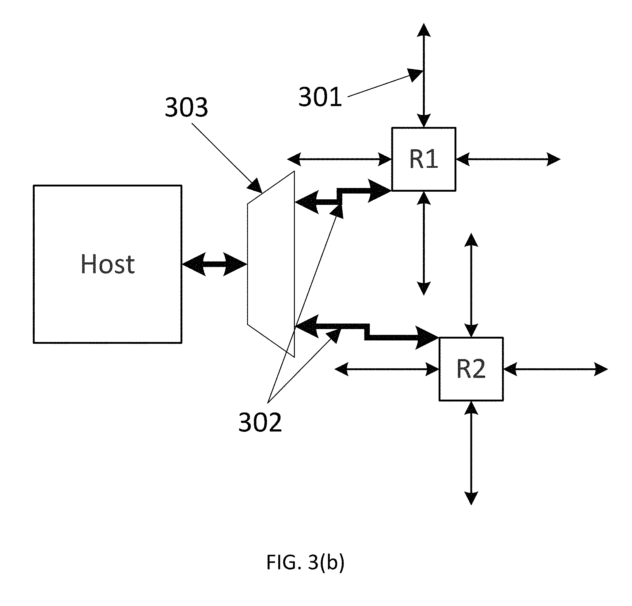
To address the above bandwidth concern, multiple parallel physical NoCs may be used. Each NoC may be called a layer, thus creating a multi-layer NoC architecture. Hosts inject a message on a NoC layer; the message is then routed to the destination on the NoC layer, where it is delivered from the NoC layer to the host. Thus, each layer operates more or less independently from each other, and interactions between layers may only occur during the injection and ejection times. FIG. 3A illustrates a two layer NoC. Here the two NoC layers are shown adjacent to each other on the left and right, with the hosts connected to the NoC replicated in both left and right diagrams. A host is connected to two routers in this example--a router in the first layer shown as R1, and a router is the second layer shown as R2. In this example, the multi-layer NoC is different from the 3D NoC, i.e. multiple layers are on a single silicon die and are used to meet the high bandwidth demands of the communication between hosts on the same silicon die. Messages do not go from one layer to another. For purposes of clarity, the present application will utilize such a horizontal left and right illustration for multi-layer NoC to differentiate from the 3D NoCs, which are illustrated by drawing the NoCs vertically over each other.
In FIG. 3B, a host connected to a router from each layer, R1 and R2 respectively, is illustrated. Each router is connected to other routers in its layer using directional ports 301, and is connected to the host using injection and ejection ports 302. A bridge-logic 303 may sit between the host and the two NoC layers to determine the NoC layer for an outgoing message and sends the message from host to the NoC layer, and also perform the arbitration and multiplexing between incoming messages from the two NoC layers and delivers them to the host.
In a multi-layer NoC, the number of layers needed may depend upon a number of factors such as the aggregate bandwidth requirement of all traffic flows in the system, the routes that are used by various flows, message size distribution, maximum channel width, etc. Once the number of NoC layers in NoC interconnect is determined in a design, different messages and traffic flows may be routed over different NoC layers. Additionally, one may design NoC interconnects such that different layers have different topologies in number of routers, channels and connectivity. The channels in different layers may have different widths based on the flows that traverse over the channel and their bandwidth requirements.
System on Chips (SoCs) are becoming increasingly sophisticated, feature rich, and high performance by integrating a growing number of standard processor cores, memory and I/O subsystems, and specialized acceleration IPs. To address this complexity, NoC approach of connecting SoC components is gaining popularity. A NoC can provide connectivity to a plethora of components and interfaces and simultaneously enable rapid design closure by being automatically generated from a high level specification. The specification describes interconnect requirements of SoC in terms of connectivity, bandwidth, and latency. In addition to this, information such as position of various components such as bridges or ports on boundary of hosts, traffic information, chip size information, etc. may be supplied. A NoC compiler (topology generation engine) can then use this specification to automatically design a NoC for the SoC. A number of NoC compilers were introduced in the related art that automatically synthesize a NoC to fit a traffic specification. In such design flows, the synthesized NoC is simulated to evaluate the performance under various operating conditions and to determine whether the specifications are met. This may be necessary because NoC-style interconnects are distributed systems and their dynamic performance characteristics under load are difficult to predict statically and can be very sensitive to a wide variety of parameters. Specifications can also be in the form of power specifications to define power domains, voltage domains, clock domains, and so on, depending on the desired implementation.
In large-scale networks, efficiency and performance/area tradeoff is of main concern. Mechanisms such as machine learning approach, simulated annealing, among others, provide optimized topology for a system. However, such complex mechanisms have substantial limitations as they involve certain algorithms to automate optimization of layout network, which may violate previously mapped flow's latency constraint or the latency constraint of current flow. Therefore, there is a need for systems and methods that significantly improve system efficiency by accurately indicating the best possible positions and configurations for hosts and ports within the hosts, along with indicating system level routes to be taken for traffic flows using the NoC interconnect architecture. Systems and methods are also required for automatically generating an optimized topology for a given SoC floor plan and traffic specification with an efficient layout. Systems and methods are also required for automatically transforming SoC floor plan and traffic specifications from physical placement into logical placement to satisfy bandwidth requirements while maintaining lowest area, lowest routing with minimum wiring and buffering cost, and latency.
Therefore, there exists a need for methods, systems, and computer readable mediums for overcoming the above-mentioned issues with existing implementations of generating topology for a given SoC.
SUMMARY
Methods and example implementations described herein are generally directed to an interconnect architecture, and more specifically, to system-on-chip (SoC) optimization through transformation and to automatically generate an optimized network-on-chip (NoC) topology for a given user specified physical topological constraints.
Aspects of the present disclosure relate to methods, systems, and computer readable mediums for overcoming the above-mentioned issues with existing implementations of generating topology for a given SoC by significantly improving system efficiency by accurately indicating the best possible positions and configurations for hosts and ports within the hosts, along with indicating system level routes to be taken for traffic flows using the NoC interconnect architecture. Further, methods, systems, and computer readable mediums automatically generate an optimized topology for a given SoC floor plan and traffic specification with an efficient layout. Furthermore, methods, systems, and computer readable mediums are also required for automatically transforming SoC floor plan and traffic specifications from physical placement into logical placement to satisfy bandwidth requirements while maintaining lowest area, lowest routing with minimum wiring and buffering cost, and latency.
An aspect of the present disclosure relates to a method for generating a Network-on-Chip (NoC) topology. The method includes the steps of receiving at least a floor plan description of a System-on-Chip (SoC), transforming said floor plan description into at least one logical grid layout of one or more rows and one or more columns, optimizing a number of said one or more rows and said one or more columns based at least on any or combination of a power, an area, or a performance to obtain an optimized transformed logical grid layout, and generating said Network-on-Chip (NoC) topology at least from said optimized transformed logical grid layout.
In an aspect, said floor plan description comprising any or combination of one or more positions of at least one host, one or more sizes of SoC, and one or more positions of at least one bridge.
In an aspect, said one or more rows and said one or more columns are determined at least from one or more corners associated with the host and/or said one or more positions of the host.
In an aspect, each intersection of said one or more rows and said one or more columns is indicative of at least a potential router location.
In an aspect, the method can further include the step of generating one or more connections on said optimized transformed logical grid layout based at least on overlapping hosts on one or more connection paths or bridges.
In an aspect, the method can further include the step of removing one or more connections on said optimized transformed logical grid layout based at least on overlapping hosts on one or more connection paths or bridges.
In an aspect, said one or more rows and said one or more columns are decided based on one or more domains, the one or more domains are selected from any or combination of a clock domain, a power domain, and a domain determined from physical constraints.
In an aspect, said floor plan description comprising traffic information, the number of said one or more rows and said one or more columns are optimized based on the traffic information. In an aspect, if a load of traffic is greater than 100% then said one or more rows and/or said one or more columns are added/merged (to increase the bandwidth). For example, if a load of traffic is greater than 100%, then candidate rows or columns can be merged if the combined load of traffic on candidate rows or columns to be merged is less than 50%. In another aspect, if a utilization of NoC channels on said one or more rows and/or one or more columns is greater than 100% then said one or more rows and/or said one or more columns are added, and if the combined utilization of NoC channels across multiple ones of said one or more rows and/or one or more columns is less than 100% then said one or more rows and/or said one or more columns are merged.
In an aspect, said step of optimizing is an iterative process involving tolerance.
In an aspect, said floor plan description comprising chip size information, the number of said one or more rows and said one or more columns are optimized based on the chip size information. In an aspect, wherein chip size information comprising information associated with a placement of one or more wires in a gap.
In an aspect, said floor plan description comprising router radix information and/or router arbitration frequency information, the number of said one or more rows and said one or more columns are optimized based on said router radix information and/or said router arbitration frequency information.
An aspect of the present disclosure relates to a system to generate a Network-on-Chip (NoC) topology. The system can include a receiving module a receiving module to receive at least a floor plan description of a System-on-Chip (SoC), a transformation module to transform said floor plan description into at least one logical grid layout of one or more rows and one or more columns, an optimization module to optimize a number of said one or more rows and said one or more columns based at least on any or combination of a power, an area, or a performance to obtain an optimized transformed logical grid layout, and an NoC generation module configured to generating said Network-on-Chip (NoC) topology at least from said optimized transformed logical grid layout.
In an aspect, said floor plan description comprising any or combination of one or more positions of at least one host, one or more sizes of SoC, and one or more positions of at least one bridge.
In an aspect, said one or more rows and said one or more columns are determined at least from one or more corners associated with the host and/or said one or more positions of the host.
In an aspect, each intersection of said one or more rows and said one or more columns is indicative of at least a potential router location.
In an aspect, said NoC generation module is further configured to generate one or more connections on said optimized transformed logical grid layout based at least on overlapping hosts on one or more connection paths or bridges.
In an aspect, said one or more rows and said one or more columns are decided based on one or more domains, the one or more domains are selected from any or combination of a clock domain, a power domain, or a performance domain.
In an aspect, said floor plan description comprising traffic information, the number of said one or more rows and said one or more columns are optimized based on the traffic information. In an aspect, if a load of traffic is greater than 100% then said one or more rows and/or said one or more columns are added/merged (to increase the bandwidth). For example, if a load of traffic is greater than 100%, then candidate rows or columns can be merged if the combined load of traffic on candidate rows or columns to be merged is less than 50%.
In an aspect, the number of said one or more rows and said one or more columns are optimized in an iterative manner involving tolerance.
In an aspect, said floor plan description comprising chip size information, the number of said one or more rows and said one or more columns are optimized based on the chip size information.
In an aspect, chip size information comprising information associated with a placement of one or more wires in a gap.
In an aspect, said floor plan description comprising router radix information and/or router arbitration frequency information, the number of said one or more rows and said one or more columns are optimized based on said router radix information and/or said router arbitration frequency information.
An aspect of the present disclosure relates to a non-transitory computer readable storage medium storing instructions for executing a process. The instructions include the steps of receiving at least a floor plan description of a System-on-Chip (SoC), transforming said floor plan description into at least one logical grid layout of one or more rows and one or more columns, optimizing a number of said one or more rows and said one or more columns based at least on any or combination of a power, an area, or a performance to obtain an optimized transformed logical grid layout, and generating said Network-on-Chip (NoC) topology at least from said optimized transformed logical grid layout.
BRIEF DESCRIPTION OF DRAWINGS
FIGS. 1A, 1B, 1C, and 1D illustrate examples of Bidirectional ring, 2D Mesh, 2D Taurus, and 3D Mesh NoC Topologies.
FIG. 2A illustrates an example of XY routing in a related art two dimensional mesh.
FIG. 2B illustrates three different routes between a source and destination nodes.
FIG. 3A illustrates an example of a related art two layer NoC interconnect.
FIG. 3B illustrates the related art bridge logic between host and multiple NoC layers.
FIGS. 4A and 4B illustrate example flow diagram for overall process for generating a Network-on-Chip (NoC) topology.
FIG. 5 illustrates example considerations for candidate rows and columns for generating a Network-on-Chip (NoC) topology.
FIGS. 6A and 6B illustrate example process for determining connections for generating a Network-on-Chip (NoC) topology.
FIG. 7 illustrates an example chip size optimization for generating a Network-on-Chip (NoC) topology.
FIG. 8 illustrates an example row and/or column merger for generating a Network-on-Chip (NoC) topology.
FIG. 9 illustrates an example flow diagram for generating a Network-on-Chip (NoC) topology.
FIG. 10 illustrates an example computer system on which example implementations may be implemented.
DETAILED DESCRIPTION
The following detailed description provides further details of the figures and example implementations of the present application. Reference numerals and descriptions of redundant elements between figures are omitted for clarity. Terms used throughout the description are provided as examples and are not intended to be limiting. For example, the use of the term "automatic" may involve fully automatic or semi-automatic implementations involving user or administrator control over certain aspects of the implementation, depending on the desired implementation of one of ordinary skill in the art practicing implementations of the present application.
Network-on-Chip (NoC) has emerged as a paradigm to interconnect a large number of components on the chip. NoC is a global shared communication infrastructure made up of several routing nodes interconnected with each other using point-to-point physical links. In example implementations, a NoC interconnect is generated from a specification by utilizing design tools. The specification can include constraints such as bandwidth/Quality of Service (QoS)/latency attributes that is to be met by the NoC, and can be in various software formats depending on the design tools utilized. Once the NoC is generated through the use of design tools on the specification to meet the specification requirements, the physical architecture can be implemented either by manufacturing a chip layout to facilitate the NoC or by generation of a register transfer level (RTL) for execution on a chip to emulate the generated NoC, depending on the desired implementation. Specifications may be in common power format (CPF), Unified Power Format (UPF), or others according to the desired specification. Specifications can be in the form of traffic specifications indicating the traffic, bandwidth requirements, latency requirements, interconnections, etc. depending on the desired implementation. Specifications can also be in the form of power specifications to define power domains, voltage domains, clock domains, and so on, depending on the desired implementation.
Methods and example implementations described herein are generally directed to an interconnect architecture, and more specifically, to system-on-chip (SoC) optimization through transformation and to automatically generate an optimized network-on-chip (NoC) topology for a given user specified physical topological constraints.
Aspects of the present disclosure relate to methods, systems, and computer readable mediums for overcoming the above-mentioned issues with existing implementations of generating topology for a given SoC by improving system efficiency by accurately indicating the best possible positions and configurations for hosts and ports within the hosts, along with indicating system level routes to be taken for traffic flows using the NoC interconnect architecture. Further, methods, systems, and computer readable mediums automatically generate an optimized topology for a given SoC floor plan and traffic specification with an efficient layout. Furthermore, methods, systems, and computer readable mediums are also required for automatically transforming SoC floor plan and traffic specifications from physical placement into logical placement to satisfy bandwidth requirements while maintaining lowest area, lowest routing with minimum wiring and buffering cost, and latency. In this manner, an efficient NoC can be generated for a given SoC floorplan, thereby obviating the need to generate, test or manufacture multiple NoCs for a given SoC to implement a NoC for a SoC floorplan.
An aspect of the present disclosure relates to a method for generating a Network-on-Chip (NoC) topology. The method includes the steps of receiving at least a floor plan description of a System-on-Chip (SoC), transforming said floor plan description into at least one logical grid layout of one or more rows and one or more columns, optimizing a number of said one or more rows and said one or more columns based at least on any or combination of a power, an area, or a performance to obtain an optimized transformed logical grid layout, and generating said Network-on-Chip (NoC) topology at least from said optimized transformed logical grid layout.
In an aspect, said floor plan description comprising any or combination of one or more positions of at least one host, one or more sizes of SoC, and one or more positions of at least one bridge.
In an aspect, said one or more rows and said one or more columns are determined at least from one or more corners associated with the host and/or said one or more positions of the host.
In an aspect, each intersection of said one or more rows and said one or more columns is indicative of at least a potential router location.
In an aspect, the method can further include the step of generating one or more connections on said optimized transformed logical grid layout based at least on overlapping hosts on one or more connection paths or bridges.
In an aspect, the method can further include the step of removing one or more connections on said optimized transformed logical grid layout based at least on overlapping hosts on one or more connection paths or bridges.
In an aspect, said one or more rows and said one or more columns are decided based on one or more domains, the one or more domains are selected from any or combination of a clock domain, a power domain, and a domain determined from physical constraints.
In an aspect, said floor plan description comprising traffic information, the number of said one or more rows and said one or more columns are optimized based on the traffic information. In an aspect, if a load of traffic is greater than 100% then said one or more rows and/or said one or more columns are added/merged (to increase the bandwidth). For example, if a load of traffic is greater than 100%, then candidate rows or columns can be merged if the combined load of traffic on candidate rows or columns to be merged is less than 50%. In another aspect, if a utilization of NoC channels on said one or more rows and/or one or more columns is greater than 100% then said one or more rows and/or said one or more columns are added, and if the combined utilization of NoC channels across multiple ones of said one or more rows and/or one or more columns is less than 100% then said one or more rows and/or said one or more columns are merged.
In an aspect, said step of optimizing is an iterative process involving tolerance.
In an aspect, said floor plan description comprising chip size information, the number of said one or more rows and said one or more columns are optimized based on the chip size information. In an aspect, wherein chip size information comprising information associated with a placement of one or more wires in a gap.
In an aspect, said floor plan description comprising router radix information and/or router arbitration frequency information, the number of said one or more rows and said one or more columns are optimized based on said router radix information and/or said router arbitration frequency information.
An aspect of the present disclosure relates to a system to generate a Network-on-Chip (NoC) topology. The system can include a receiving module a receiving module to receive at least a floor plan description of a System-on-Chip (SoC), a transformation module to transform said floor plan description into at least one logical grid layout of one or more rows and one or more columns, an optimization module to optimize a number of said one or more rows and said one or more columns based at least on any or combination of a power, an area, or a performance to obtain an optimized transformed logical grid layout, and an NoC generation module configured to generating said Network-on-Chip (NoC) topology at least from said optimized transformed logical grid layout.
In an aspect, said floor plan description comprising any or combination of one or more positions of at least one host, one or more sizes of SoC, and one or more positions of at least one bridge.
In an aspect, said one or more rows and said one or more columns are determined at least from one or more corners associated with the host and/or said one or more positions of the host.
In an aspect, each intersection of said one or more rows and said one or more columns is indicative of at least a potential router location.
In an aspect, said NoC generation module is further configured to generate one or more connections on said optimized transformed logical grid layout based at least on overlapping hosts on one or more connection paths or bridges.
In an aspect, said one or more rows and said one or more columns are decided based on one or more domains, the one or more domains are selected from any or combination of a clock domain, a power domain, or a performance domain.
In an aspect, said floor plan description comprising traffic information, the number of said one or more rows and said one or more columns are optimized based on the traffic information. In an aspect, if a load of traffic is greater than 100% then said one or more rows and/or said one or more columns are added/merged (to increase the bandwidth). For example, if a load of traffic is greater than 100%, then candidate rows or columns can be merged if the combined load of traffic on candidate rows or columns to be merged is less than 50%.
In an aspect, the number of said one or more rows and said one or more columns are optimized in an iterative manner involving tolerance.
In an aspect, said floor plan description comprising chip size information, the number of said one or more rows and said one or more columns are optimized based on the chip size information.
In an aspect, chip size information comprising information associated with a placement of one or more wires in a gap.
In an aspect, said floor plan description comprising router radix information and/or router arbitration frequency information, the number of said one or more rows and said one or more columns are optimized based on said router radix information and/or said router arbitration frequency information.
An aspect of the present disclosure relates to a non-transitory computer readable storage medium storing instructions for executing a process. The instructions include the steps of receiving at least a floor plan description of a System-on-Chip (SoC), transforming said floor plan description into at least one logical grid layout of one or more rows and one or more columns, optimizing a number of said one or more rows and said one or more columns based at least on any or combination of a power, an area, or a performance to obtain an optimized transformed logical grid layout, and generating said Network-on-Chip (NoC) topology at least from said optimized transformed logical grid layout.
FIGS. 4A and 4B illustrate example flow diagram for overall process, for generating a Network-on-Chip (NoC) topology, for automatic generation of NoC from specified topological information/constraints based on projecting NoC elements onto a grid layout by projecting a plurality of nodes, a plurality of routers, and a plurality of links onto the grid layout based on the specified topological information, wherein the projected plurality of routers, the plurality of nodes, and the plurality of links are initially disabled, and then selectively enabling for at least one of the plurality of routers, the plurality of nodes, and the plurality of links on the grid layout based on one or more constraints for one or more layers of the NoC.
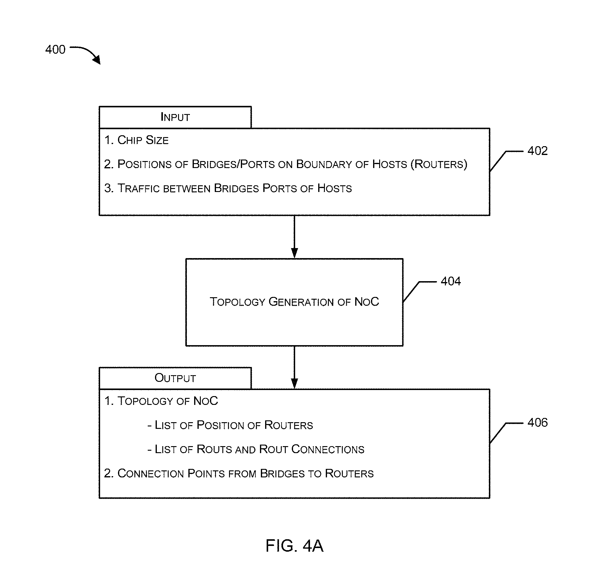
FIGS. 4A and 4B illustrates an example representation showing automatic generation of NoC from specified topological information/constraints based on projecting NoC elements onto a grid layout by projecting a plurality of nodes, a plurality of routers, and a plurality of links onto the grid layout based on the specified topological information, wherein the projected plurality of routers, the plurality of nodes, and the plurality of links are initially disabled, and then selectively enabling for at least one of the plurality of routers, the plurality of nodes, and the plurality of links on the grid layout based on one or more constraints for one or more layers of the NoC. The grid represents a plurality of routers and bridges that are configured on the grid initially, and then links there between are then selectively enabled between specific routers and/or bridges by activation of their links. For instance, although multiple routers and bridges have been configured, links for only links 402 and 404 have been activated. Once enabled, NoC agents can be provided on the enabled ones of the plurality of nodes of the grid layout and traffic can be provided between the provided NoC agents. In another aspect, traffic to the enabled ones of the plurality of routers and the plurality of links of the NoC can also be mapped.
As shown in FIG. 4A, in an implementation 400, a topology generation of NoC block 404, which can include an NoC compiler, receives various inputs associated with the physical placement to a coarse grain grid for NoC construction from an input block 402. In an example implementation, a number of NoC compilers are introduced in the related art that automatically synthesize a NoC to fit a traffic specification. In such design flows, the synthesized NoC is simulated to evaluate the performance under various operating conditions and to determine whether the specifications are met. This may be necessary because NoC-style interconnects are distributed systems and their dynamic performance characteristics under load are difficult to predict statically and can be very sensitive to a wide variety of parameters.
In an example implementation, the input block 402 can provide information associated with a chip size as input along with positions of bridges, ports on boundary of hosts (router), and traffic information between bridges or ports of the hosts, as inputs.
In an implementation, the topology generations of NoC block 404 then use this specification to automatically design a NoC for the SoC. In an example implementation, the topology generation of NoC block 404 generates a topology of NoC having a list of positions associated with routers, and list of routers and associated route connections. Apart from the topology of NoC, the topology generation of NoC block 404 also generates connection points from bridges to routers (as shown in FIG. 5).
In an example implementation, by achieving the output at block 406, the implementations described herein optimizes bandwidth/latency constraints, cost (wire/buffer) constraints, timing of components, all traffic that has a path through NoC, radix limit of routers, channel widths, and etc.
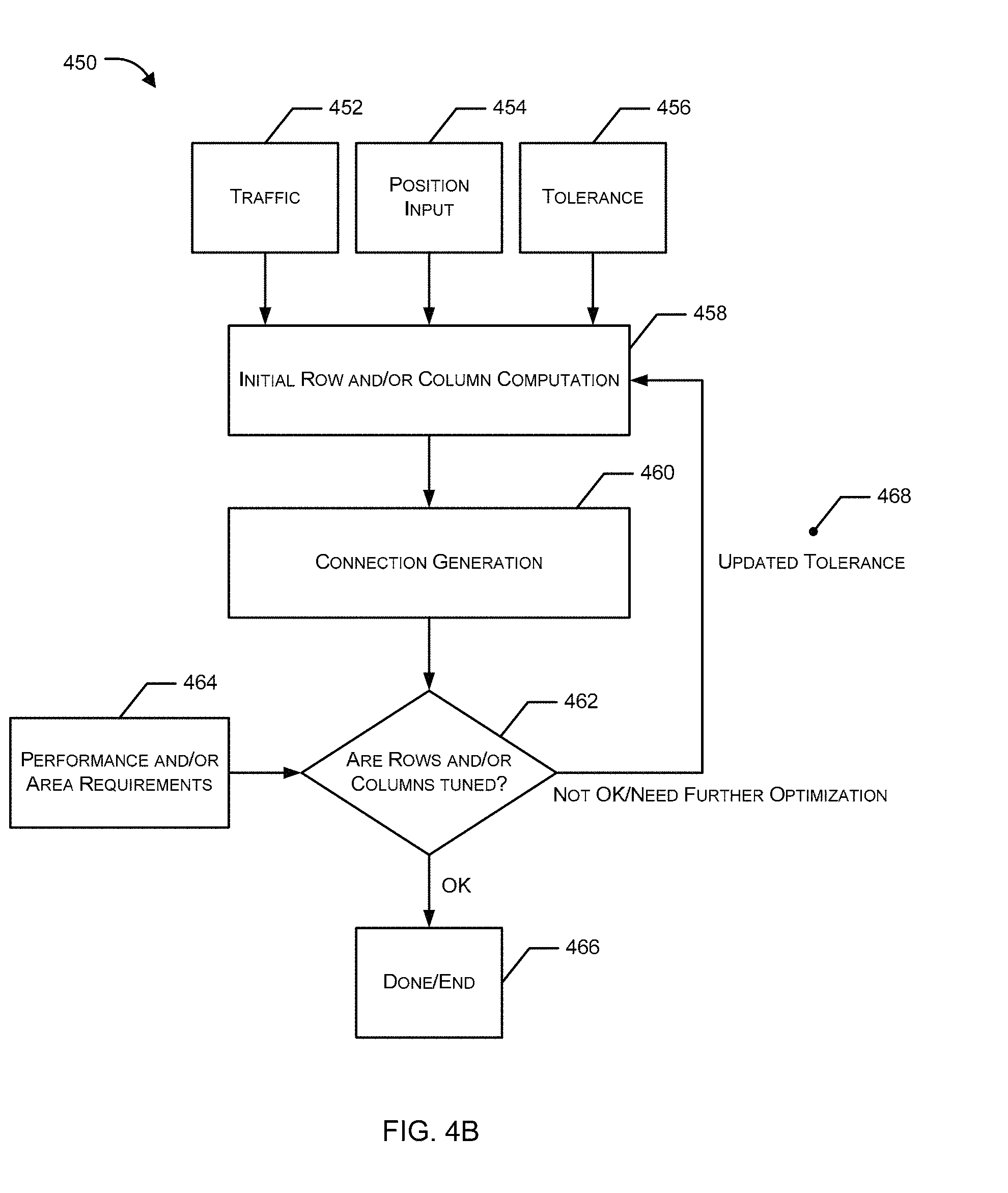
Referring now to FIG. 4B, an example flow diagram 450 for overall process, for generating a Network-on-Chip (NoC) topology. As shown in FIG. 4B, in an implementation, a plurality of inputs, such as but not limited to, traffic 452 information, position input 454 associated with routers/hosts, and information associated with tolerance 456, are provided as input for computing initial rows and/or columns at block 458.
In an example implementation, the initial rows and/or columns computed at block 458 are provided for connection generation at block 460 which generates tuned/optimized rows and columns at block 462. The tuned/optimized rows and columns at block 462 while optimizing also considers performance and/or area requirement provided from block 464. If the rows and columns are the most optimized/tuned, the process is stopped at block 466. However, if the rows and columns are not most optimized/tuned, the updated tolerance 478 is provided as input and the rows and columns are processed to achieve most optimized/tuned rows and columns.
In an example implementation, the method according to the present disclosure enables to achieve SoC optimization through transformation and generation of NoC topology thereof. In an example implementation, the method according to the present disclosure enables to simplify the unnecessary details of the design to solve for latency and wire costs in the physical world. Since the output generated can accurately identify topology of NoC including list of positions for routers, list of router to router connections and Connection points from Bridges to Routers.
FIG. 5 illustrates example considerations for candidate rows and columns for generating a Network-on-Chip (NoC) topology. One should appreciate that the compression mechanisms disclosed herein are completely example in nature and any other technique can be used to create the flattened virtual grid, all of which are completely within the scope of the present disclosure.
In an implementation 500, FIG. 5 illustrates example representations showing automatic generation of NoC from specified topological information/constraints based on projecting NoC elements onto one or more grid layouts by projecting a plurality of routers, a plurality of links, and a plurality of NoC agents onto a grid layout based on one or more constraints for one or more layers of the NoC and the specified topological information, wherein grid sizes of the heterogeneous grid layout are derived from the specified topological information. As shown, original input layout of NoC agents 516, 518, 524, 526, 532, and 534 can be directly transitioned to an equal column width layout, wherein spacing along the X-axis (depicting grid sizes) is same and represents a homogeneous grid layout where the routers and/or the bridges are configured based on their configuration in terms of space, distance, position, and construction in the real space. Once arranged on the homogeneous grid layout, traffic can be provided between the plurality of NoC agents and the traffic can be mapped to the NoC.
In an example implementation, as shown the grid representation from the original input, wherein the representation shows a heterogeneous grid layout having different width sizes based on alignment, topological information/constraints, position, location, among other parameters of the NoC agent. As further shown, a heterogeneous grid layout can further be automatically converted into a grid layout by projecting an auto-determined grid on a plurality of routers, a plurality of links, and a plurality of NoC agents based on the specified topological information, and providing traffic between the plurality of NoC agents and mapping the traffic to the NoC. As show the representation comprises projection of router/bridge attributes such as location, construction, links, position, space, onto the auto-determined grid that has equal spacing and sizing as regards the X-axis. The present implementation therefore enables determination of the grid based on business specification based on real coordinate and not the grid coordinates, wherein based on different types of specifications, the proposed system automatically transitions the real space to a constrained grid.
In an example implementation, given a specification with hosts sizes, shapes, positions, ports and bridges (where bridges will be in terms of physical size (e.g., 10 um, 20 um, etc.)) the present disclosure enables to construct columns and rows that are in units of x um columns and y um rows.
In an example implementation, the columns and rows are formed from host corners, bridge positions, and domain corners. Differing domains cannot be merged.
In an example implementation, the present disclosure enables to mark every corner of a host as a column for shortest path routing (example, mark bridges at 100 um, 400 um, 570 um, 1000 um, 1700 um, 2000 umm, positions of all of the columns, which indicates maximum columns required.
In an example implementation, the present disclosure enables to shrink to the optimum value for the given traffic based on a tolerance (minimum width of a row or column), grid does not have to have equal size columns or rows, and each row or column can be its own size in accordance with the desired implementation. The tolerance also does not need to be the same for all rows or all columns, each row or each column can have its own tolerance depending on the desired implementation. For example, based on tolerance of 500 um, example implementations can start at a tolerance of 100 um, make widths 500 um, so 100, 400 and 570 are in the same column and connected to the same router. However, if router has insufficient ports, then it needs to be extended to another column with another router.
In an example implementation, the present disclosure enables to mark each row based on position of the bridges thereby reducing rows and columns to reduce area. User inputs a tolerance value whereas the present disclosure enables to calculate actual tolerance i.e., two tolerances.
In an example implementation, the present disclosure also enables to check all traffic that has a path through the NoC and radix limit of routers is not exceeded. If not, more columns are needed, and the bridges need to be spaced further apart. Accordingly, the present disclosure enables to determine actual tolerance for recalculating/re-computing rows/columns and checks if the NoC layout is optimized in nature.
In an example implementation, the NoC can be tuned to meet the smallest possible NOC to meet the performance. Accordingly, wires can be routed over blocks depending on number of layers available and how many layers the block occupies.
In an example implementation, as shown in FIG. 5, a plurality of routers 516, 518, 524, 526, 532, and 534 can be located in various columns 504 and various rows 502 as stated above (i.e., columns and rows that are in units of x um columns and y um rows) based on the positions of the hosts 506, 508, 510. Mark every corner of a host as a column for shortest path routing represented by 512, 514, 520, 522, 528 and 530. For example, bridges are marked at 100 um, 400 um, 570 um, 1000 um, 1700 um, 2000 um i.e., positions of all of the columns indicating maximum columns required.
In an example implementation, the columns and rows are formed from host corners, bridge positions, and domain corners. Differing domains cannot be merged.
In an implementation, wires can be routed over blocks depending on number of layers available and how many layers the block occupies. FIGS. 6A and 6B illustrate example process for determining connections for generating a Network-on-Chip (NoC) topology.
In an example implementation, for determining connections, as shown in FIG. 6A 600 and FIG. 6B 650, if a wire 606 being initiated form source router 602 attempting to reach to a destination router 604 passes through an opaque (transparent and/or translucent) block 604 as shown in FIG. 6A, then according to the present disclosure, it should not be a permissible connection. Also, it is a possibility that the wire 652 routs around opaque (transparent and/or translucent) block 604 as shown in FIG. 6b, but if there is already rows routing above and below, then the present disclosure eliminates extra connections as for optimization purposes, there should be at most one wire routed around each edge of the IP.
Thus, the present disclosure facilitates the positioning of the hosts, the bridges and the boundaries of the hosts to transform the physical specification into a logical design for the SoC that has a grid structure fundamentally with some edges removed and with the bridges being connected to appropriate boundaries within that grid structure and that topology, and resulting in a topology that facilitates a NoC in some dimensional area. Accordingly, the host has ports connected to the bridge having its protocol translated into the protocol of the NoC, and ports are on the boundaries of the hosts.
Thus, the present disclosure achieves, transformation from physical placement to logical placement to satisfy bandwidth requirements while maintaining the lowest area and lowest routing with minimum cost (wiring and buffering) and latency.
FIG. 7 illustrates an example chip size optimization for generating a Network-on-Chip (NoC) topology. In an implementation 700, the present disclosure facilitates various ways of chip optimization. In an example implementation, one method is without tolerance. In this method, in order to decide a performance optimization of the chip, example implementations start with a full mesh and then reduce number of rows and columns based on load on channels (e.g., if load is <5% for a particular part of the mesh, then merge the mesh as long as enough bisectional bandwidth and available connections). Further, columns can be added based on the bisectional bandwidth if needed. Example implementations can check the load of a channel, and if load is >100% then more columns are added, but if they have less than 100% load, then the columns or rows are merged to see if load is still <100%.
While doing the area optimization, through use of rows and columns, rows and columns can be split based on performance. Example methods to split the rows or columns can include dividing them evenly, through simulated annealing, or through other methods in accordance with the desired implementation.
In an example implementation, merging of rows or columns may be decided by comparing best possible merges based on desired criteria (e.g., peak load), and the merges of such rows or columns are conducted. For example, example implementations can examine n rows and m columns for n+m potential mergers, and traverse such mergers until merges are determined not to be good. Splitting of rows or columns can involve selecting the worst load or cost (e.g., by position, density) and then split.
In an example implementation, one method is with tolerance. In this method, tolerance includes the wiring cost, clock domains/power domains (places constraints as clock/power domains that are not the same type cannot be merged), and changing frequencies, voltage, and so on, when transformed into the logical layout. In example implementations the domains can be carried over so that every domain edge is a column and row.
In an example implementation, optimization of chip size can be based on gaps between each pair of hosts or between host and an edge of the chip. Gaps are wiring channels involving some number of wires that increases or decreases the size of the chip. Caches, routers, and other components of the NoC may also occupy space within the gaps. The present disclosure includes implementations to shrink dimensions by minimizing number of wires between each of the gaps, which may result in a reduced chip size.
In example, as shown in FIG. 7, a chip size layout of an un-optimized chip is illustrated. As shown in FIG. 7, g1-16 are various gaps that are present in the chip whereas h1-h5 is the widths of various routers. Wires W1-W2 passes through the gaps as shown in FIG. 7, such wiring further adds to the chip size. Gaps are wiring channels involving some number of wires that increases or decreases the size of the chip. Accordingly, a maximum width of the chip size can be calculated as combination of gaps present in the layout and widths of the each router. The actual width of any chip size can be obtained based at least on gaps between each pair of hosts or between host and an edge of the chip. The present disclosure can include implementations to shrink dimensions by minimizing number of wires between each of the gaps, thereby resulting in a reduced chip size.
FIG. 8 illustrates an example row and/or column merger for generating a Network-on-Chip (NoC) topology. In an example implementation 800, FIG. 8 shows rows and columns optimization based on various factors. In an example implementation, the columns and rows are formed from host corners, bridge positions, and domain corners. Differing domains cannot be merged.
As shown in FIG. 8, various hosts 802-810 can be present at various location, thus, if a load of traffic is greater than 100% then said one or more rows and/or said one or more columns are/merged (to increase the bandwidth). For example, if a load of traffic is greater than 100%, then candidate rows or columns can be merged if the combined load of traffic on candidate rows or columns to be merged is less than 50%.
FIG. 9 illustrates an example flow diagram 900 for generating a Network-on-Chip (NoC) topology. In an implementation, the present disclosure relates to a method for generating a Network-on-Chip (NoC) topology. The method at step 902 receives at least a floor plan description of a System-on-Chips (SoC). The method at step 904 transforms said floor plan description into at least one logical grid layout of one or more rows and one or more columns. The method at step 906 optimizes a number of said one or more rows and said one or more columns based at least on any or combination of a power, an area, or a performance to obtain an optimized transformed logical grid layout. The method at step 908 generates said Network-on-Chip (NoC) topology at least from said optimized transformed logical grid layout.
In an example implementation, said floor plan description comprising any or combination of one or more positions of at least one host, one or more sizes of SoC, and one or more positions of at least one bridge.
In an example implementation, said one or more rows and said one or more columns are determined at least from one or more corners associated with the host and/or said one or more positions of the host.
In an example implementation, each intersection of said one or more rows and said one or more columns is indicative of at least a potential router location.
In an example implementation, the method can further include the step of generating one or more connections on said optimized transformed logical grid layout based at least on overlapping hosts on one or more connection paths or bridges.
In an example implementation, said one or more rows and said one or more columns are decided based on one or more domains, the one or more domains are selected from any or combination of a clock domain, a power domain, or a performance domain.
In an example implementation, said floor plan description comprising traffic information, the number of said one or more rows and said one or more columns are optimized based on the traffic information. In an aspect, if a load of traffic is greater than 100% then said one or more rows and/or said one or more columns are added/merged (to increase the bandwidth). For example, if a load of traffic is greater than 100%, then candidate rows or columns can be merged if the combined load of traffic on candidate rows or columns to be merged is less than 50%.
In an example implementation, said step of optimizing is an iterative process involving tolerance.
In an example implementation, said floor plan description comprising chip size information, the number of said one or more rows and said one or more columns are optimized based on the chip size information. In an aspect, wherein chip size information comprising information associated with a placement of one or more wires in a gap.
In an example implementation, said floor plan description comprising router radix information and/or router arbitration frequency information, the number of said one or more rows and said one or more columns are optimized based on said router radix information and/or said router arbitration frequency information.
FIG. 10 illustrates an example computer system on which example implementations may be implemented. This example system is merely illustrative, and other modules or functional partitioning may therefore be substituted as would be understood by those skilled in the art. Further, this system may be modified by adding, deleting, or modifying modules and operations without departing from the scope of the inventive concept.
In an aspect, computer system 1000 includes a server 1002 that may involve an I/O unit 1012, storage 1016, and a processor 1004 operable to execute one or more units as known to one skilled in the art. The term "computer-readable medium" as used herein refers to any medium that participates in providing instructions to processor 1004 for execution, which may come in the form of computer-readable storage mediums, such as, but not limited to optical disks, magnetic disks, read-only memories, random access memories, solid state devices and drives, or any other types of tangible media suitable for storing electronic information, or computer-readable signal mediums, which can include transitory media such as carrier waves. The I/O unit processes input from user interfaces 1018 and operator interfaces 1020 which may utilize input devices such as a keyboard, mouse, touch device, or verbal command
The server 1002 may also be connected to an external storage 1022, which can contain removable storage such as a portable hard drive, optical media (CD or DVD), disk media or any other medium from which a computer can read executable code. The server may also be connected an output device 1024, such as a display to output data and other information to a user, as well as request additional information from a user. The connections from the server 1002 to the user interface 1018, the operator interface 1024, the external storage 1016, and the output device 1024 may via wireless protocols, such as the 802.11 standards, Bluetooth.RTM. or cellular protocols, or via physical transmission media, such as cables or fiber optics. The output device 1024 may therefore further act as an input device for interacting with a user.
The processor 1004 may execute one or more modules including a receiving module 1006 a receiving module to receive at least a floor plan description of an System-on-Chips (SoC), a transformation module 1008 to transform said floor plan description into at least one logical grid layout of one or more rows and one or more columns, an optimization module 1010 to optimize a number of said one or more rows and said one or more columns based at least on any or combination of a power, an area, or a performance to obtain an optimized transformed logical grid layout, and an NoC generation module 1012 to generating said Network-on-Chip (NoC) topology at least from said optimized transformed logical grid layout.
Unless specifically stated otherwise, as apparent from the discussion, it is appreciated that throughout the description, discussions utilizing terms such as "processing," "computing," "calculating," "determining," "displaying," or the like, can include the actions and processes of a computer system or other information processing device that manipulates and transforms data represented as physical (electronic) quantities within the computer system's registers and memories into other data similarly represented as physical quantities within the computer system's memories or registers or other information storage, transmission or display devices.
Example implementations may also relate to an apparatus for performing the operations herein. This apparatus may be specially constructed for the required purposes, or it may include one or more general-purpose computers selectively activated or reconfigured by one or more computer programs. Such computer programs may be stored in a computer readable medium, such as a computer-readable storage medium or a computer-readable signal medium. A computer-readable storage medium may involve tangible mediums such as, but not limited to optical disks, magnetic disks, read-only memories, random access memories, solid state devices and drives, or any other types of tangible or non-transitory media suitable for storing electronic information. A computer readable signal medium may include mediums such as carrier waves. The algorithms and displays presented herein are not inherently related to any particular computer or other apparatus. Computer programs can involve pure software implementations that involve instructions that perform the operations of the desired implementation.
Various general-purpose systems may be used with programs and modules in accordance with the examples herein, or it may prove convenient to construct a more specialized apparatus to perform desired method steps. In addition, the example implementations are not described with reference to any particular programming language. It will be appreciated that a variety of programming languages may be used to implement the teachings of the example implementations as described herein. The instructions of the programming language(s) may be executed by one or more processing devices, e.g., central processing units (CPUs), processors, or controllers.
As is known in the art, the operations described above can be performed by hardware, software, or some combination of software and hardware. Various aspects of the example implementations may be implemented using circuits and logic devices (hardware), while other aspects may be implemented using instructions stored on a machine-readable medium (software), which if executed by a processor, would cause the processor to perform a method to carry out implementations of the present disclosure. Further, some example implementations of the present disclosure may be performed solely in hardware, whereas other example implementations may be performed solely in software. Moreover, the various functions described can be performed in a single unit, or can be spread across a number of components in any number of ways. When performed by software, the methods may be executed by a processor, such as a general purpose computer, based on instructions stored on a computer-readable medium. If desired, the instructions can be stored on the medium in a compressed and/or encrypted format.
Moreover, other implementations of the present application will be apparent to those skilled in the art from consideration of the specification and practice of the example implementations disclosed herein. Various aspects and/or components of the described example implementations may be used singly or in any combination. It is intended that the specification and examples be considered as examples, with a true scope and spirit of the application being indicated by the following claims.
* * * * *
D00000
D00001
D00002
D00003
D00004
D00005
D00006
D00007
D00008
D00009
D00010
D00011
D00012
D00013
D00014

D00015

D00016

XML
uspto.report is an independent third-party trademark research tool that is not affiliated, endorsed, or sponsored by the United States Patent and Trademark Office (USPTO) or any other governmental organization. The information provided by uspto.report is based on publicly available data at the time of writing and is intended for informational purposes only.
While we strive to provide accurate and up-to-date information, we do not guarantee the accuracy, completeness, reliability, or suitability of the information displayed on this site. The use of this site is at your own risk. Any reliance you place on such information is therefore strictly at your own risk.
All official trademark data, including owner information, should be verified by visiting the official USPTO website at www.uspto.gov. This site is not intended to replace professional legal advice and should not be used as a substitute for consulting with a legal professional who is knowledgeable about trademark law.