Wafer carrier for reducing contamination from carbon particles and outgassing
Chae , et al.
U.S. patent number 10,309,012 [Application Number 14/712,741] was granted by the patent office on 2019-06-04 for wafer carrier for reducing contamination from carbon particles and outgassing. This patent grant is currently assigned to Tesla, Inc.. The grantee listed for this patent is SolarCity Corporation. Invention is credited to Yongkee Chae, Jianming Fu, Jiunn Benjamin Heng, Zheng Xu.


View All Diagrams
| United States Patent | 10,309,012 |
| Chae , et al. | June 4, 2019 |
Wafer carrier for reducing contamination from carbon particles and outgassing
Abstract
A wafer carrier for carrying solar cell wafers during a deposition process is described. The carrier is coated with pyrolytic carbon, silicon carbide, or a ceramic material, and is adapted to receive and support the wafers.
| Inventors: | Chae; Yongkee (San Ramon, CA), Heng; Jiunn Benjamin (San Jose, CA), Fu; Jianming (Palo Alto, CA), Xu; Zheng (Pleasanton, CA) | ||||||||||
|---|---|---|---|---|---|---|---|---|---|---|---|
| Applicant: |
|
||||||||||
| Assignee: | Tesla, Inc. (Palo Alto,
CA) |
||||||||||
| Family ID: | 55016604 | ||||||||||
| Appl. No.: | 14/712,741 | ||||||||||
| Filed: | May 14, 2015 |
Prior Publication Data
| Document Identifier | Publication Date | |
|---|---|---|
| US 20160002774 A1 | Jan 7, 2016 | |
Related U.S. Patent Documents
| Application Number | Filing Date | Patent Number | Issue Date | ||
|---|---|---|---|---|---|
| 62020957 | Jul 3, 2014 | ||||
| Current U.S. Class: | 1/1 |
| Current CPC Class: | H01L 21/68757 (20130101); C23C 16/4404 (20130101); C23C 16/4581 (20130101); H01L 21/6875 (20130101); H01L 21/68771 (20130101); C23C 16/4585 (20130101); H01L 21/68735 (20130101) |
| Current International Class: | C23C 16/458 (20060101); C23C 16/44 (20060101); H01L 21/687 (20060101) |
References Cited [Referenced By]
U.S. Patent Documents
| 819360 | March 1902 | Mayer |
| 2626907 | January 1953 | Melvin De Groote |
| 2938938 | May 1960 | Dickson |
| 3094439 | June 1963 | Mann |
| 3116171 | December 1963 | Nielson |
| 3459597 | August 1969 | Baron |
| 3676179 | July 1972 | Bokros |
| 3961997 | June 1976 | Chu |
| 3969163 | July 1976 | Wakefield |
| 4015280 | March 1977 | Matsushita |
| 4082568 | April 1978 | Lindmayer |
| 4124410 | November 1978 | Kotval |
| 4124455 | November 1978 | Lindmayer |
| 4193975 | March 1980 | Kotval |
| 4200621 | April 1980 | Liaw |
| 4213798 | July 1980 | Williams |
| 4228315 | October 1980 | Napoli |
| 4251285 | February 1981 | Yoldas |
| 4284490 | August 1981 | Weber |
| 4315096 | February 1982 | Tyan |
| 4336648 | June 1982 | Pschunder |
| 4342044 | July 1982 | Ovshinsky |
| 4431858 | February 1984 | Gonzalez |
| 4514579 | April 1985 | Hanak |
| 4540843 | September 1985 | Gochermann |
| 4567642 | February 1986 | Dilts |
| 4571448 | February 1986 | Barnett |
| 4577051 | March 1986 | Hartman |
| 4586988 | May 1986 | Nath |
| 4589191 | May 1986 | Green |
| 4612409 | September 1986 | Hamakawa |
| 4617421 | October 1986 | Nath |
| 4633033 | December 1986 | Nath |
| 4652693 | March 1987 | Bar-On |
| 4657060 | April 1987 | Kaucic |
| 4667060 | May 1987 | Spitzer |
| 4670096 | June 1987 | Schwirtlich |
| 4694115 | September 1987 | Lillington |
| 4729970 | March 1988 | Nath |
| 4753683 | June 1988 | Ellion |
| 4771017 | September 1988 | Tobin |
| 4784702 | November 1988 | Henri |
| 4877460 | October 1989 | Flodl |
| 4933061 | June 1990 | Kulkarni |
| 4968384 | November 1990 | Asano |
| 5053355 | October 1991 | von Campe |
| 5057163 | October 1991 | Barnett |
| 5075763 | December 1991 | Spitzer |
| 5084107 | January 1992 | Deguchi |
| 5118361 | June 1992 | Fraas |
| 5131933 | July 1992 | Floedl |
| 5155051 | October 1992 | Noguchi |
| 5178685 | January 1993 | Borenstein |
| 5181968 | January 1993 | Nath |
| 5213628 | May 1993 | Noguchi |
| 5217539 | June 1993 | Fraas |
| 5279682 | January 1994 | Wald |
| 5286306 | February 1994 | Menezes |
| 5364518 | November 1994 | Hartig |
| 5401331 | March 1995 | Ciszek |
| 5455430 | October 1995 | Noguchi |
| 5461002 | October 1995 | Safir |
| 5563092 | October 1996 | Ohmi |
| 5576241 | November 1996 | Sakai |
| 5627081 | May 1997 | Tsuo |
| 5676766 | October 1997 | Probst |
| 5681402 | October 1997 | Ichinose |
| 5698451 | December 1997 | Hanoka |
| 5705828 | January 1998 | Noguchi |
| 5726065 | March 1998 | Szlufcik |
| 5808315 | September 1998 | Murakami |
| 5814195 | September 1998 | Lehan |
| 5903382 | May 1999 | Tench |
| 5935345 | August 1999 | Kuznicki |
| 5942048 | August 1999 | Fujisaki |
| 6017581 | January 2000 | Hooker |
| 6034322 | March 2000 | Pollard |
| 6091019 | July 2000 | Sakata |
| 6140570 | October 2000 | Kariya |
| 6232545 | May 2001 | Samaras |
| 6303853 | October 2001 | Fraas |
| 6333457 | December 2001 | Mulligan |
| 6408786 | June 2002 | Kennedy |
| 6410843 | June 2002 | Kishi |
| 6441297 | August 2002 | Keller |
| 6468828 | October 2002 | Glatfelter |
| 6488824 | December 2002 | Hollars |
| 6538193 | March 2003 | Fraas |
| 6552414 | April 2003 | Horzel |
| 6586270 | July 2003 | Tsuzuki |
| 6620645 | September 2003 | Chandra |
| 6672018 | January 2004 | Shingleton |
| 6683360 | January 2004 | Dierickx |
| 6736948 | May 2004 | Barrett |
| 6761771 | July 2004 | Satoh |
| 6803513 | October 2004 | Beernink |
| 6841051 | January 2005 | Crowley |
| 6917755 | July 2005 | Nguyen |
| 7030413 | April 2006 | Nakamura |
| 7128975 | October 2006 | Inomata |
| 7164150 | January 2007 | Terakawa |
| 7328534 | February 2008 | Dinwoodie |
| 7388146 | June 2008 | Fraas |
| 7399385 | July 2008 | German |
| 7534632 | May 2009 | Hu |
| 7635810 | December 2009 | Luch |
| 7737357 | June 2010 | Cousins |
| 7749883 | July 2010 | Meeus |
| 7769887 | August 2010 | Bhattacharyya |
| 7772484 | August 2010 | Li |
| 7777128 | August 2010 | Montello |
| 7825329 | November 2010 | Basol |
| 7829781 | November 2010 | Montello |
| 7829785 | November 2010 | Basol |
| 7872192 | January 2011 | Fraas |
| 7905995 | March 2011 | German |
| 7977220 | July 2011 | Sanjurjo |
| 8070925 | December 2011 | Hoffman |
| 8115093 | February 2012 | Gui |
| 8119901 | February 2012 | Jang |
| 8152536 | April 2012 | Scherer |
| 8168880 | May 2012 | Jacobs |
| 8182662 | May 2012 | Crowley |
| 8196360 | June 2012 | Metten |
| 8209920 | July 2012 | Krause |
| 8222513 | July 2012 | Luch |
| 8222516 | July 2012 | Cousins |
| 8258050 | September 2012 | Cho |
| 8343795 | January 2013 | Luo |
| 8569096 | October 2013 | Babayan |
| 8586857 | November 2013 | Everson |
| 8671630 | March 2014 | Lena |
| 8686283 | April 2014 | Heng |
| 8815631 | August 2014 | Cousins |
| 9029181 | May 2015 | Rhodes |
| 9147788 | September 2015 | DeGroot |
| 9287431 | March 2016 | Mascarenhas |
| 9761744 | September 2017 | Wang |
| 2001/0008143 | July 2001 | Sasaoka |
| 2001/0023702 | September 2001 | Nakagawa |
| 2002/0015881 | February 2002 | Nakamura |
| 2002/0072207 | June 2002 | Andoh |
| 2002/0086456 | July 2002 | Cunningham |
| 2002/0176404 | November 2002 | Girard |
| 2002/0189939 | December 2002 | German |
| 2003/0000568 | January 2003 | Gonsiorawski |
| 2003/0000571 | January 2003 | Wakuda |
| 2003/0034062 | February 2003 | Stern |
| 2003/0042516 | March 2003 | Forbes |
| 2003/0070705 | April 2003 | Hayden |
| 2003/0097447 | May 2003 | Johnston |
| 2003/0116185 | June 2003 | Oswald |
| 2003/0118865 | June 2003 | Marks |
| 2003/0121228 | July 2003 | Stoehr |
| 2003/0136440 | July 2003 | Machida |
| 2003/0168578 | September 2003 | Taguchi |
| 2003/0183270 | October 2003 | Falk |
| 2003/0201007 | October 2003 | Fraas |
| 2004/0035458 | February 2004 | Beernink |
| 2004/0065363 | April 2004 | Fetzer |
| 2004/0094196 | May 2004 | Shaheen |
| 2004/0103937 | June 2004 | Bilyalov |
| 2004/0112419 | June 2004 | Boulanger |
| 2004/0112426 | June 2004 | Hagino |
| 2004/0123897 | July 2004 | Ojima |
| 2004/0126213 | July 2004 | Pelzmann |
| 2004/0135979 | July 2004 | Hazelton |
| 2004/0152326 | August 2004 | Inomata |
| 2004/0185683 | September 2004 | Nakamura |
| 2004/0200520 | October 2004 | Mulligan |
| 2005/0009319 | January 2005 | Abe |
| 2005/0012095 | January 2005 | Niira |
| 2005/0022746 | February 2005 | Lampe |
| 2005/0022861 | February 2005 | Rose |
| 2005/0061665 | March 2005 | Pavani |
| 2005/0062041 | March 2005 | Terakawa |
| 2005/0064247 | March 2005 | Sane |
| 2005/0074954 | April 2005 | Yamanaka |
| 2005/0109388 | May 2005 | Murakami |
| 2005/0126622 | June 2005 | Mukai |
| 2005/0133084 | June 2005 | Joge |
| 2005/0178662 | August 2005 | Wurczinger |
| 2005/0189015 | September 2005 | Rohatgi |
| 2005/0199279 | September 2005 | Yoshimine |
| 2005/0252544 | November 2005 | Rohatgi |
| 2005/0257823 | November 2005 | Zwanenburg |
| 2005/0263178 | December 2005 | Montello |
| 2005/0268963 | December 2005 | Jordan |
| 2006/0012000 | January 2006 | Estes |
| 2006/0060238 | March 2006 | Hacke |
| 2006/0060791 | March 2006 | Hazelton |
| 2006/0130891 | June 2006 | Carlson |
| 2006/0154389 | July 2006 | Doan |
| 2006/0213548 | September 2006 | Bachrach |
| 2006/0231803 | October 2006 | Wang |
| 2006/0255340 | November 2006 | Manivannan |
| 2006/0260673 | November 2006 | Takeyama |
| 2006/0272698 | December 2006 | Durvasula |
| 2006/0283496 | December 2006 | Okamoto |
| 2006/0283499 | December 2006 | Terakawa |
| 2007/0023081 | February 2007 | Johnson |
| 2007/0023082 | February 2007 | Manivannan |
| 2007/0029186 | February 2007 | Krasnov |
| 2007/0108437 | May 2007 | Tavkhelidze |
| 2007/0110975 | May 2007 | Schneweis |
| 2007/0132034 | June 2007 | Curello |
| 2007/0137699 | June 2007 | Manivannan |
| 2007/0148336 | June 2007 | Bachrach |
| 2007/0186853 | August 2007 | Gurary |
| 2007/0186968 | August 2007 | Nakauchi |
| 2007/0186970 | August 2007 | Takahashi |
| 2007/0187652 | August 2007 | Konno |
| 2007/0202029 | August 2007 | Burns |
| 2007/0235077 | October 2007 | Nagata |
| 2007/0235829 | October 2007 | Levine |
| 2007/0256728 | November 2007 | Cousins |
| 2007/0274504 | November 2007 | Maes |
| 2007/0283996 | December 2007 | Hachtmann |
| 2007/0283997 | December 2007 | Hachtmann |
| 2008/0000522 | January 2008 | Johnson |
| 2008/0011350 | January 2008 | Luch |
| 2008/0035489 | February 2008 | Allardyce |
| 2008/0041436 | February 2008 | Lau |
| 2008/0041437 | February 2008 | Yamaguchi |
| 2008/0047602 | February 2008 | Krasnov |
| 2008/0047604 | February 2008 | Korevaar |
| 2008/0053519 | March 2008 | Pearce |
| 2008/0061293 | March 2008 | Ribeyron |
| 2008/0092942 | April 2008 | Kinsey |
| 2008/0092947 | April 2008 | Lopatin |
| 2008/0121272 | May 2008 | Besser |
| 2008/0121276 | May 2008 | Lopatin |
| 2008/0121932 | May 2008 | Ranade |
| 2008/0128013 | June 2008 | Lopatin |
| 2008/0128017 | June 2008 | Ford |
| 2008/0149161 | June 2008 | Nishida |
| 2008/0149163 | June 2008 | Gangemi |
| 2008/0156370 | July 2008 | Abdallah |
| 2008/0173347 | July 2008 | Korevaar |
| 2008/0173350 | July 2008 | Choi |
| 2008/0178928 | July 2008 | Warfield |
| 2008/0196757 | August 2008 | Yoshimine |
| 2008/0202577 | August 2008 | Hieslmair |
| 2008/0202582 | August 2008 | Noda |
| 2008/0216891 | September 2008 | Harkness |
| 2008/0223439 | September 2008 | Deng |
| 2008/0230122 | September 2008 | Terakawa |
| 2008/0251114 | October 2008 | Tanaka |
| 2008/0251117 | October 2008 | Schubert |
| 2008/0264477 | October 2008 | Moslehi |
| 2008/0276983 | November 2008 | Drake |
| 2008/0283115 | November 2008 | Fukawa |
| 2008/0302030 | December 2008 | Stancel |
| 2008/0303503 | December 2008 | Wolfs |
| 2008/0308145 | December 2008 | Krasnov |
| 2009/0007965 | January 2009 | Rohatgi |
| 2009/0014055 | January 2009 | Beck |
| 2009/0056805 | March 2009 | Barnett |
| 2009/0065043 | March 2009 | Hadorn |
| 2009/0078318 | March 2009 | Meyers |
| 2009/0084439 | April 2009 | Lu |
| 2009/0101872 | April 2009 | Young |
| 2009/0120492 | May 2009 | Sinha |
| 2009/0139512 | June 2009 | Lima |
| 2009/0151771 | June 2009 | Kothari |
| 2009/0151783 | June 2009 | Lu |
| 2009/0155028 | June 2009 | Boguslayskiy |
| 2009/0160259 | June 2009 | Ravindranath |
| 2009/0188561 | July 2009 | Aiken |
| 2009/0194233 | August 2009 | Tamura |
| 2009/0211627 | August 2009 | Meier |
| 2009/0221111 | September 2009 | Frolov |
| 2009/0229660 | September 2009 | Takizawa |
| 2009/0229854 | September 2009 | Fredenberg |
| 2009/0239331 | September 2009 | Xu |
| 2009/0250108 | October 2009 | Zhou |
| 2009/0255574 | October 2009 | Yu |
| 2009/0272419 | November 2009 | Sakamoto |
| 2009/0283138 | November 2009 | Lin |
| 2009/0283145 | November 2009 | Kim |
| 2009/0293948 | December 2009 | Tucci |
| 2009/0301549 | December 2009 | Moslehi |
| 2009/0308439 | December 2009 | Adibi |
| 2009/0317934 | December 2009 | Scherff |
| 2009/0320897 | December 2009 | Shimomura |
| 2010/0006145 | January 2010 | Lee |
| 2010/0015756 | January 2010 | Weidman |
| 2010/0043863 | February 2010 | Wudu |
| 2010/0065111 | March 2010 | Fu |
| 2010/0068890 | March 2010 | Stockum |
| 2010/0084009 | April 2010 | Carlson |
| 2010/0087031 | April 2010 | Veschetti |
| 2010/0108134 | May 2010 | Ravi |
| 2010/0116325 | May 2010 | Nikoonahad |
| 2010/0124619 | May 2010 | Xu |
| 2010/0131108 | May 2010 | Meyer |
| 2010/0132774 | June 2010 | Borden |
| 2010/0132792 | June 2010 | Kim |
| 2010/0147364 | June 2010 | Gonzalez |
| 2010/0154869 | June 2010 | Oh |
| 2010/0169478 | July 2010 | Saha |
| 2010/0175743 | July 2010 | Gonzalez |
| 2010/0186802 | July 2010 | Borden |
| 2010/0193014 | August 2010 | Johnson |
| 2010/0218799 | September 2010 | Stefani |
| 2010/0224230 | September 2010 | Luch |
| 2010/0229914 | September 2010 | Adriani |
| 2010/0236612 | September 2010 | Khajehoddin |
| 2010/0240172 | September 2010 | Rana |
| 2010/0243021 | September 2010 | Lee |
| 2010/0243059 | September 2010 | Okaniwa |
| 2010/0269904 | October 2010 | Cousins |
| 2010/0279492 | November 2010 | Yang |
| 2010/0282293 | November 2010 | Meyer |
| 2010/0295091 | November 2010 | Strzegowski |
| 2010/0300506 | December 2010 | Heng |
| 2010/0300507 | December 2010 | Heng |
| 2010/0300525 | December 2010 | Lim |
| 2010/0313877 | December 2010 | Bellman |
| 2010/0326518 | December 2010 | Juso |
| 2011/0005569 | January 2011 | Sauar |
| 2011/0005920 | January 2011 | Ivanov |
| 2011/0023958 | February 2011 | Masson |
| 2011/0030777 | February 2011 | Lim |
| 2011/0048491 | March 2011 | Taira |
| 2011/0056545 | March 2011 | Ji |
| 2011/0073175 | March 2011 | Hilali |
| 2011/0088762 | April 2011 | Singh |
| 2011/0089079 | April 2011 | Lo |
| 2011/0120518 | May 2011 | Rust |
| 2011/0146759 | June 2011 | Lee |
| 2011/0146781 | June 2011 | Laudisio |
| 2011/0156188 | June 2011 | Tu |
| 2011/0168250 | July 2011 | Lin |
| 2011/0168261 | July 2011 | Welser |
| 2011/0174374 | July 2011 | Harder |
| 2011/0177648 | July 2011 | Tanner |
| 2011/0186112 | August 2011 | Aernouts |
| 2011/0220182 | September 2011 | Lin |
| 2011/0245957 | October 2011 | Porthouse |
| 2011/0259419 | October 2011 | Hagemann |
| 2011/0272012 | November 2011 | Heng |
| 2011/0277688 | November 2011 | Trujillo |
| 2011/0277816 | November 2011 | Xu |
| 2011/0277825 | November 2011 | Fu et al. |
| 2011/0284064 | November 2011 | Engelhart |
| 2011/0297224 | December 2011 | Miyamoto |
| 2011/0297227 | December 2011 | Pysch |
| 2011/0300661 | December 2011 | Pearce |
| 2011/0308573 | December 2011 | Jaus |
| 2012/0000502 | January 2012 | Wiedeman |
| 2012/0012153 | January 2012 | Azechi |
| 2012/0012174 | January 2012 | Wu |
| 2012/0028461 | February 2012 | Ritchie |
| 2012/0031480 | February 2012 | Tisler |
| 2012/0040487 | February 2012 | Asthana |
| 2012/0042925 | February 2012 | Pfennig |
| 2012/0060911 | March 2012 | Fu |
| 2012/0073975 | March 2012 | Ganti |
| 2012/0080083 | April 2012 | Liang |
| 2012/0085384 | April 2012 | Beitel |
| 2012/0122262 | May 2012 | Kang |
| 2012/0125391 | May 2012 | Pinarbasi |
| 2012/0145233 | June 2012 | Syn |
| 2012/0152349 | June 2012 | Cao |
| 2012/0152752 | June 2012 | Keigler |
| 2012/0167986 | July 2012 | Meakin |
| 2012/0180851 | July 2012 | Nagel |
| 2012/0192932 | August 2012 | Wu |
| 2012/0199184 | August 2012 | Nie |
| 2012/0240995 | September 2012 | Coakley |
| 2012/0248497 | October 2012 | Zhou |
| 2012/0279443 | November 2012 | Kornmeyer |
| 2012/0279548 | November 2012 | Munch |
| 2012/0285517 | November 2012 | Souza |
| 2012/0305060 | December 2012 | Fu et al. |
| 2012/0318319 | December 2012 | Pinarbasi |
| 2012/0318340 | December 2012 | Heng |
| 2012/0319253 | December 2012 | Mizuno |
| 2012/0325282 | December 2012 | Snow |
| 2013/0000705 | January 2013 | Shappir |
| 2013/0014802 | January 2013 | Zimmerman |
| 2013/0019919 | January 2013 | Hoang |
| 2013/0056051 | March 2013 | Jin |
| 2013/0096710 | April 2013 | Pinarbasi |
| 2013/0112239 | May 2013 | Liptac |
| 2013/0130430 | May 2013 | Moslehi |
| 2013/0139878 | June 2013 | Bhatnagar |
| 2013/0152996 | June 2013 | DeGroot |
| 2013/0160826 | June 2013 | Beckerman |
| 2013/0174897 | July 2013 | You |
| 2013/0199608 | August 2013 | Emeraud |
| 2013/0206213 | August 2013 | He |
| 2013/0206219 | August 2013 | Kurtin |
| 2013/0206221 | August 2013 | Gannon |
| 2013/0213469 | August 2013 | Kramer |
| 2013/0220401 | August 2013 | Scheulov |
| 2013/0228221 | September 2013 | Moslehi |
| 2013/0239891 | September 2013 | Sonoda |
| 2013/0247955 | September 2013 | Baba |
| 2013/0269771 | October 2013 | Cheun |
| 2013/0291743 | November 2013 | Endo |
| 2013/0306128 | November 2013 | Kannou |
| 2014/0000682 | January 2014 | Zhao |
| 2014/0053899 | February 2014 | Haag |
| 2014/0060621 | March 2014 | Clark |
| 2014/0066265 | March 2014 | Oliver |
| 2014/0096823 | April 2014 | Fu |
| 2014/0102524 | April 2014 | Xie |
| 2014/0120699 | May 2014 | Hua |
| 2014/0124013 | May 2014 | Morad |
| 2014/0124014 | May 2014 | Morad |
| 2014/0154836 | June 2014 | Kim |
| 2014/0196768 | July 2014 | Heng |
| 2014/0242746 | August 2014 | Albadri |
| 2014/0261624 | September 2014 | Cruz-Campa |
| 2014/0261654 | September 2014 | Babayan |
| 2014/0261661 | September 2014 | Babayan |
| 2014/0262793 | September 2014 | Babayan |
| 2014/0273338 | September 2014 | Kumar |
| 2014/0284750 | September 2014 | Yu |
| 2014/0299187 | October 2014 | Chang |
| 2014/0318611 | October 2014 | Moslehi |
| 2014/0345674 | November 2014 | Yang |
| 2014/0349441 | November 2014 | Fu |
| 2014/0352777 | December 2014 | Hachtmann |
| 2015/0007879 | January 2015 | Kwon |
| 2015/0020877 | January 2015 | Moslehi |
| 2015/0075599 | March 2015 | Yu |
| 2015/0090314 | April 2015 | Yang |
| 2015/0096613 | April 2015 | Tjahjono |
| 2015/0114444 | April 2015 | Lentine |
| 2015/0129024 | May 2015 | Brainard |
| 2015/0144180 | May 2015 | Baccini |
| 2015/0171230 | June 2015 | Kapur |
| 2015/0207011 | July 2015 | Garnett |
| 2015/0214409 | July 2015 | Pfeiffer |
| 2015/0236177 | August 2015 | Fu |
| 2015/0270410 | September 2015 | Heng |
| 2015/0280641 | October 2015 | Garg |
| 2015/0325731 | November 2015 | Namjoshi |
| 2015/0333199 | November 2015 | Kim |
| 2015/0340531 | November 2015 | Hayashi |
| 2015/0349145 | December 2015 | Morad |
| 2015/0349153 | December 2015 | Morad |
| 2015/0349161 | December 2015 | Morad |
| 2015/0349162 | December 2015 | Morad |
| 2015/0349167 | December 2015 | Morad |
| 2015/0349168 | December 2015 | Morad |
| 2015/0349169 | December 2015 | Morad |
| 2015/0349170 | December 2015 | Morad |
| 2015/0349171 | December 2015 | Morad |
| 2015/0349172 | December 2015 | Morad |
| 2015/0349173 | December 2015 | Morad |
| 2015/0349174 | December 2015 | Morad |
| 2015/0349175 | December 2015 | Morad |
| 2015/0349176 | December 2015 | Morad |
| 2015/0349190 | December 2015 | Morad |
| 2015/0349193 | December 2015 | Morad |
| 2015/0349701 | December 2015 | Morad |
| 2015/0349702 | December 2015 | Morad |
| 2015/0349703 | December 2015 | Morad |
| 2016/0163888 | June 2016 | Reddy |
| 2016/0190354 | June 2016 | Agrawal |
| 2016/0204289 | July 2016 | Tao |
| 2016/0233353 | August 2016 | Tamura |
| 2016/0268963 | September 2016 | Tsai |
| 2016/0322513 | November 2016 | Martin |
| 2016/0329443 | November 2016 | Wang |
| 2017/0084766 | March 2017 | Yang |
| 2017/0162722 | June 2017 | Fu |
| 2017/0222082 | August 2017 | Lin |
| 2017/0288081 | October 2017 | Babayan |
| 2017/0373204 | December 2017 | Corneille |
| 2018/0122964 | May 2018 | Adachi |
| 1253381 | May 2000 | CN | |||
| 1416179 | Oct 2001 | CN | |||
| 101233620 | Jul 2008 | CN | |||
| 101553933 | Oct 2009 | CN | |||
| 100580957 | Jan 2010 | CN | |||
| 101305454 | May 2010 | CN | |||
| 102088040 | Jun 2011 | CN | |||
| 102263157 | Nov 2011 | CN | |||
| 104205347 | Dec 2014 | CN | |||
| 104409402 | Mar 2015 | CN | |||
| 4030713 | Apr 1992 | DE | |||
| 102006009194 | Aug 2007 | DE | |||
| 202007002897 | Aug 2008 | DE | |||
| 102008045522 | Mar 2010 | DE | |||
| 102010061317 | Jun 2012 | DE | |||
| 10201201051 | Nov 2013 | DE | |||
| 102012010151 | Nov 2013 | DE | |||
| 1770791 | Apr 2007 | EP | |||
| 1806684 | Aug 2007 | EP | |||
| 2071635 | Jun 2009 | EP | |||
| 2113946 | Nov 2009 | EP | |||
| 2362430 | Aug 2011 | EP | |||
| 2385561 | Nov 2011 | EP | |||
| 2385561 | Nov 2011 | EP | |||
| 2387079 | Nov 2011 | EP | |||
| 2479796 | Jul 2012 | EP | |||
| 2626907 | Aug 2013 | EP | |||
| 2479796 | Jul 2015 | EP | |||
| 2626907 | Aug 2015 | EP | |||
| 5789269 | Jun 1982 | JP | |||
| S7089269 | Jun 1982 | JP | |||
| H04245683 | Sep 1992 | JP | |||
| 06196766 | Jul 1994 | JP | |||
| H07249788 | Sep 1995 | JP | |||
| 10004204 | Jan 1998 | JP | |||
| H1131834 | Feb 1999 | JP | |||
| 2000164902 | Jun 2000 | JP | |||
| 2002057357 | Feb 2002 | JP | |||
| 2005159312 | Jun 2005 | JP | |||
| 2006523025 | Oct 2006 | JP | |||
| 2006324504 | Nov 2006 | JP | |||
| 2007123792 | May 2007 | JP | |||
| 2008135655 | Jun 2008 | JP | |||
| 2009054748 | Mar 2009 | JP | |||
| 2009177225 | Aug 2009 | JP | |||
| 2011181966 | Sep 2011 | JP | |||
| 2012119393 | Jun 2012 | JP | |||
| 2013526045 | Jun 2013 | JP | |||
| 2013161855 | Aug 2013 | JP | |||
| 2013536512 | Sep 2013 | JP | |||
| 2013537000 | Sep 2013 | JP | |||
| 2013219378 | Oct 2013 | JP | |||
| 2013233553 | Nov 2013 | JP | |||
| 2013239694 | Nov 2013 | JP | |||
| 2013247231 | Dec 2013 | JP | |||
| 20050122721 | Dec 2005 | KR | |||
| 20060003277 | Jan 2006 | KR | |||
| 20090011519 | Feb 2009 | KR | |||
| 1991017839 | Nov 1991 | WO | |||
| 9120097 | Dec 1991 | WO | |||
| 2003083953 | Oct 2003 | WO | |||
| 2006097189 | Sep 2006 | WO | |||
| 2008089657 | Jul 2008 | WO | |||
| 2009094578 | Jul 2009 | WO | |||
| 2009150654 | Dec 2009 | WO | |||
| 2009150654 | Dec 2009 | WO | |||
| 2010070015 | Jun 2010 | WO | |||
| 2010075606 | Jul 2010 | WO | |||
| 2010075606 | Jul 2010 | WO | |||
| 2010104726 | Sep 2010 | WO | |||
| 2010123974 | Oct 2010 | WO | |||
| 2010123974 | Oct 2010 | WO | |||
| 2011005447 | Jan 2011 | WO | |||
| 2011005447 | Jan 2011 | WO | |||
| 2011008881 | Jan 2011 | WO | |||
| 2011008881 | Jan 2011 | WO | |||
| 2011053006 | May 2011 | WO | |||
| 2011123646 | Oct 2011 | WO | |||
| 2013020590 | Feb 2013 | WO | |||
| 2013020590 | Feb 2013 | WO | |||
| 2010085949 | Mar 2013 | WO | |||
| 2013046351 | Apr 2013 | WO | |||
| 2014066265 | May 2014 | WO | |||
| 2014074826 | Jul 2014 | WO | |||
| 2014110520 | Jul 2014 | WO | |||
| 2014117138 | Jul 2014 | WO | |||
| 2015183827 | Dec 2015 | WO | |||
| 2015195283 | Dec 2015 | WO | |||
| 2016090332 | Jun 2016 | WO | |||
Other References
|
Parthavi, "Doping by Diffusion and Implantation", <http://www.leb.eei.uni-erlangen.de/winterakademie/2010/report/course0- 3/pdf/0306.pdf>. cited by applicant . Weiss, "Development of different copper seed layers with respect to the copper electroplating process," Microelectronic Engineering 50 (2000) 443-440, Mar. 15, 2000. cited by applicant . Tomasi, "Back-contacted Silicon Heterojunction Solar Cells With Efficiency>21%" 2014 IEEE. cited by applicant . Hornbachner et al., "Cambered Photovoltaic Module and Method for its Manufacture" Jun. 17, 2009. cited by applicant . Machine translation of JP 10004204 A, Shindou et al. cited by applicant . Jianhua Zhao et al. "24% Efficient perl silicon solar cell: Recent improvements in high efficiency silicon cell research". cited by applicant . "Nonequilibrium boron doping effects in low-temperature epitaxial silicon" Meyerson et al., Appl. Phys. Lett. 50 (2), p. 113 (1987). cited by applicant . "Doping Diffusion and Implantation" Parthavi, <http://www.leb.eei.uni-erlangen.de/winterakademie/2010/report/content- /course03/pdf/0306.pdf>. cited by applicant . WP Leroy et al., "In Search for the Limits of Rotating Cylindrical Magnetron Sputtering", Magnetron, ION Processing and ARC Technologies European Conference, Jun. 18, 2010, pp. 1-32. cited by applicant . Beaucarne G et al: `Epitaxial thin-film Si solar cells` Thin Solid Films, Elsevier-Sequoia S.A. Lausanne, CH LNKD--DOI:10.1016/J.TSF.2005.12.003, vol. 511-512, Jul. 26, 2006 (Jul. 26, 2006), pp. 533-542, XP025007243 ISSN: 0040-6090 [retrieved on Jul. 26, 2006]. cited by applicant . Chabal, Yves J. et al., `Silicon Surface and Interface Issues for Nanoelectronics,` The Electrochemical Society Interface, Spring 2005, pp. 31-33. cited by applicant . Collins English Dictionary (Convex. (2000). In Collins English Dictionary. http://search.credoreference.com/content/entry/hcengdict/convex/0 on Oct. 18, 2014). cited by applicant . Cui, `Chapter 7 Dopant diffusion`, publically available as early as Nov. 4, 2010 at <https://web.archive.org/web/20101104143332/http://ece.uwaterloo.ca/.a- bout.bcui/content/NE/%020343/Chapter/%207%20Dopant%20 diffusion%20_%20I.pptx> and converted to PDF. cited by applicant . Davies, P.C.W., `Quantum tunneling time,` Am. J. Phys. 73, Jan. 2005, pp. 23-27. cited by applicant . Dosaj V D et al: `Single Crystal Silicon Ingot Pulled From Chemically-Upgraded Metallurgical-Grade Silicon` Conference Record of the IEEE Photovoltaic Specialists Conference, May 6, 1975 (May 6, 1975), pp. 275-279, XP001050345. cited by applicant . Green, Martin A. et al., `High-Efficiency Silicon Solar Cells,` IEEE Transactions on Electron Devices, vol. ED-31, No. 5, May 1984, pp. 679-683. cited by applicant . Hamm, Gary, Wei, Lingyum, Jacques, Dave, Development of a Plated Nickel Seed Layer for Front Side Metallization of Silicon Solar Cells, EU PVSEC Proceedings, Presented Sep. 2009. cited by applicant . JCS Pires, J Otubo, AFB Braga, PR Mei; The purification of metallurgical grade silicon by electron beam melting, J of Mats Process Tech 169 (2005) 16-20. cited by applicant . Khattak, C. P. et al., "Refining Molten Metallurgical Grade Silicon for use as Feedstock for Photovoltaic Applications", 16th E.C. Photovoltaic Solar Energy Conference, May 1-5, 2000, pp. 1282-1283. cited by applicant . Merriam-Webster online dictionary--"mesh". (accessed Oct. 8, 2012). cited by applicant . Mueller, Thomas, et al. "Application of wide-band gap hydrogenated amorphous silicon oxide layers to heterojunction solar cells for high quality passivation." Photovoltaic Specialists Conference, 2008. PVSC'08. 33rd IEEE. IEEE, 2008. cited by applicant . Mueller, Thomas, et al. "High quality passivation for heteroj unction solar cells by hydrogenated amorphous silicon suboxide films." Applied Physics Letters 92.3 (2008): 033504-033504. cited by applicant . Munzer, K.A. "High Throughput Industrial In-Line Boron BSF Diffusion" Jun. 2005. 20th European Photovoltaic Solar Energy Conference, pp. 777-780. cited by applicant . National Weather Service Weather Forecast Office ("Why Do We have Seasons?" http://www.crh.noaa.gov/lmk/?n=seasons Accessed Oct. 18, 2014). cited by applicant . O'Mara, W.C.; Herring, R.B.; Hunt L.P. (1990). Handbook of Semiconductor Silicon Technology. William Andrew Publishing/Noyes. pp. 275-293. cited by applicant . Roedern, B. von, et al., `Why is the Open-Circuit Voltage of Crystalline Si Solar Cells so Critically Dependent on Emitter-and Base-Doping?` Presented at the 9th Workshop on Crystalline Silicon Solar Cell Materials and Processes, Breckenridge, CO, Aug. 9-11, 1999. cited by applicant . Stangl et al., Amorphous/Crystalline Silicon heterojunction solar cells--a simulation study; 17th European Photovoltaic Conference, Munich, Oct. 2001. cited by applicant . Warabisako T et al: `Efficient Solar Cells From Metallurgical-Grade Silicon` Japanese Journal of Applied Physics, Japan Society of Applied Physics, JP, vol. 19, No. Suppl. 19-01, Jan. 1, 1980 (Jan. 1, 1980), pp. 539-544, XP008036363 ISSN: 0021-4922. cited by applicant . Yao Wen-Jie et al: `Interdisciplinary Physics and Related Areas of Science and Technology;The p recombination layer in tunnel junctions for micromorph tandem solar cells`, Chinese Physics B, Chinese Physics B, Bristol GB, vol. 20, No. 7, Jul. 26, 2011 (Jul. 26, 2011), p. 78402, XP02020739, ISSN: 1674-1056, DOI: 10.1088/1674-1056/20/7/078402. cited by applicant . Cui, `Chapter 7 Dopant diffusion`, publically available as early as Nov. 4, 2010 at <https://web.archive.org/web/20101104143332/http://ece.uwaterloo.ca/.a- bout.bcui/content/NE/%20343/Chapter/%207%20Dopant%20 diffusion%20_%20I.pptx> and converted to PDF. cited by applicant . Yao Wen-Jie et al: `Interdisciplinary Physics and Related Areas of Science and Technology; The p recombination layer in tunnel junctions for micromorph tandem solar cells`, Chinese Physics B, Chinese Physics B, Bristol GB, vol. 20, No. 7, Jul. 26, 2011 (Jul. 26, 2011), p. 78402, XP020207379, ISSN: 1674-1056, DOI: 10.1088/1674-1056/20/7/078402. cited by applicant . Cui, et al., Advanced Materials, 2001, col. 13, pp. 1476-1480 (Year:2001). cited by applicant . Electrically Conductive Foil Tape for Bus Bar Components in Photovoltaic Modules, Adhesives Research, http://www.adhesivesresearch.com/electrically-conductive-foil-tape-for-bu- s-bar-components-in-photovoltaic-modules/, accessed Oct. 12, 2017. cited by applicant . Geissbuhler et al., Silicon Heterojunction solar Cells with Copper-Plated Grid Electrodes: Status and Comparison with Silver Thick-Film Techniques, IEEE Journal of Photovoltaics, vol. 4, No. 4, Jul. 2014. cited by applicant . Kanani, Nasser. Electroplating: Basic Principles, Processes and Practice, Chapter 8--"Coating Thickness and its Measurement," 2004, pp. 247-291. cited by applicant . P. Borden et al. "Polysilicon Tunnel Junctions as Alternates to Diffused Junctions" Proceedings of the 23rd European Photovoltaic Solar Energy Conference, Sep. 1, 2008-Sep. 5, 2008, pp. 1149-1152. cited by applicant . L. Korte et al. "Overview on a-Se:H/c heterojunction solar cells--physics and technology", Proceedings of the 22nd European Photovoltaic Solar Energy Conference, Sep. 3, 2007-Sep. 7, 2007, pp. 859-865. cited by applicant . Meyerson et al. "Nonequilibrium boron doping effects in low-temperature epitaxial silicon", Appl. Phys. Lett. 50 (2), p. 113 (1987). cited by applicant . Li, "Surface and Bulk Passsivation of Multicrystalline Silicon Solar Cells by Silicon Nitride (H) Layer: Modeling and Experiments", Ph.D. dissertation, N.J. Inst. of Tech., Jan 2009. cited by applicant. |
Primary Examiner: Lee; Aiden
Attorney, Agent or Firm: Yao; Shun Park, Vaughan, Fleming & Dowler LLP
Parent Case Text
RELATED APPLICATION
This application claims the benefit of U.S. Provisional Application No. 62/020,957, entitled "Method and System for Preventing Formation of Carbon Particles or Outgas sing from CVD Carrier by Pyrolytic Carbon Coating," by inventors Yongkee Chae, Jiunn Benjamin Heng, Jianming Fu, and Zheng Xu, filed 3 Jul. 2014.
Claims
What is claimed is:
1. An apparatus for carrying one or more wafers, the apparatus comprising: a carrier coated with a pyrolytic carbon layer: wherein the carrier comprises a number of pockets configured to accommodate the wafers, wherein a respective pocket has a ridged bottom comprising a number of ridges, wherein a top edge of a respective ridge is rounded, and wherein a radius of the rounded top edge is at least 0.1 mm; wherein the pyrolytic carbon layer has a porosity between 0 and 0.1%; wherein at least one edge of the carrier comprises an L-shaped interlocking mechanism that has a horizontal portion and a vertical portion; and wherein the L-shaped interlocking mechanism is configured to interlock with a corresponding L-shaped interlocking mechanism of an adjacent carrier, thereby facilitating an interlocked joint between the carrier and the adjacent carrier to prevent relative lateral shifts between the carrier and the adjacent carrier.
2. The apparatus of claim 1, wherein the carrier comprises graphite or carbon fiber composite.
3. The apparatus of claim 1, wherein the pyrolytic carbon layer has a thickness between 10 and 50 micrometers.
4. The apparatus of claim 1, wherein the carrier is adapted to accommodate the wafers of a size and shape of: a 5-inch by 5-inch square; a 6-inch by 6-inch square; a 5-inch by 5-inch pseudo-square; or a 6-inch by 6-inch pseudo-square.
5. The apparatus of claim 1, wherein edges around and within the respective pocket are rounded.
6. The apparatus of claim 1, wherein the respective pocket comprises a sloped ramp along the pocket's rim, thereby facilitating wafer loading.
7. A semiconductor deposition tool, comprising: a deposition chamber; and a carrier coated with a pyrolytic carbon layer: wherein the carrier comprises a number of pockets configured to accommodate the wafers, wherein a respective pocket has a ridged bottom comprising a number of ridges, wherein a top edge of a respective ridge is rounded, and wherein a radius of the rounded top edge is at least 0.1 mm; wherein the pyrolytic carbon layer has a porosity between 0 and 0.1%; wherein at least one edge of the carrier comprises an L-shaped interlocking mechanism that has a horizontal portion and a vertical portion; and wherein the L-shaped interlocking mechanism is configured to interlock with a corresponding L-shaped interlocking mechanism of an adjacent carrier, thereby facilitating an interlocked joint between the carrier and the adjacent carrier to prevent relative lateral shifts between the carrier and the adjacent carrier.
8. The deposition tool of claim 7, wherein the carrier comprises graphite or carbon fiber composite.
9. The deposition tool of claim 7, wherein the pyrolytic carbon layer has a thickness between 10 and 50 micrometers.
10. The deposition tool of claim 7, wherein is the carrier is adapted to accommodate the wafers of a size and shape of: a 5-inch by 5-inch square; a 6-inch by 6-inch square; a 5-inch by 5-inch pseudo-square; or a 6-inch by 6-inch pseudo-square.
11. The deposition tool of claim 7, wherein edges around and within the respective pocket are rounded.
12. The deposition tool of claim 7, wherein the respective pocket comprises a sloped ramp along the pocket's rim, thereby facilitating wafer loading.
Description
BACKGROUND
Field
This disclosure is generally related to the design of wafer carriers used in the fabrication of semiconductor devices. More specifically, this disclosure is related to wafer carriers used for large-scale manufacturing of solar cells.
Related Art
Crystalline-silicon based solar cells have been shown to have superb energy conversion efficiency. While device design and fabrication techniques continue to mature, and with the price of crystalline silicon becoming progressively lower, solar panels are being offered at historical low prices. In addition, with newly available financing plans and government subsidies, customers, both residential and commercial, now have unprecedented incentives to install solar panels. As a result, the solar market is expected to experience double-digit growth for many years to come.
Most of the current solar cell manufacturing facilities, however, are insufficiently equipped for large-scale production. The emerging solar market demands factories that can produce hundreds of megawatts, if not gigawatts, of solar cells per year. The design, size, and throughput of present facilities are not intended for such high-volume manufacturing. Hence, various new designs in the manufacturing process are needed.
SUMMARY
One embodiment of the present invention provides a wafer carrier for carrying solar cell wafers during a deposition process. The carrier is coated with pyrolytic carbon, silicon carbide, or a ceramic material, and is adapted to receive and support the wafers.
In a variation on this embodiment, the carrier comprises graphite or carbon fiber composite.
In a variation on this embodiment, the carrier is coated with pyrolytic carbon layer with a thickness between 10 and 50 micrometers.
In a variation on this embodiment, the pocket is configured to retain a wafer supported by the carrier that is a 5-inch by 5-inch square, a 6-inch by 6-inch square, a 5-inch by 5-inch pseudo-square, or a 6-inch by 6-inch pseudo-square.
In a variation on this embodiment, the carrier includes one or more pockets for retaining the wafers. The bottom of a respective pocket is partially carved out. The uncarved portion of the bottom has a flat top surface to support a wafer.
In a variation on this embodiment, the bottom of a respective pocket comprises a number of flat-top ridges or pillars for supporting a wafer.
In a variation on this embodiment, edges around and within a respective pocket are rounded.
In a variation on this embodiment, a respective pocket includes a sloped ramp along the pocket's rim, thereby facilitating wafer loading.
In a variation on this embodiment, the carrier includes an interlocking mechanism on at least one edge, thereby facilitating interlocking with a second carrier to form a wafer carrier system.
BRIEF DESCRIPTION OF THE FIGURES
FIG. 1 shows a diagram illustrating the electroluminescence image of a Si-based solar cell that was fabricated by being placed directly on a conventional graphite carrier during PECVD.
FIG. 2 shows a diagram illustrating the electroluminescence image of a Si-based solar cell fabricated by a PECVD process that involves non-direct contact between the wafer and a graphite carrier according to one embodiment of the present invention.
FIG. 3 shows a diagram illustrating the normalized maximum power output of solar cells that are fabricated under two different conditions according to one embodiment of the present invention.
FIG. 4 shows a diagram illustrating the measured minority carrier lifetimes (MCLs) for solar cells that are fabricated using different carriers, according to one embodiment of the present invention.
FIG. 5 shows a diagram illustrating an exemplary wafer carrier, according to an embodiment of the present invention.
FIG. 6 shows a diagram illustrating a cross-sectional view of an exemplary wafer carrier, according to an embodiment of the present invention.
FIG. 7 shows a diagram illustrating a wafer pocket with a ridged bottom according to an embodiment of the present invention.
FIG. 8 shows an exemplary cross section of a ridged-bottom wafer pocket, according to one embodiment of the present invention.
FIG. 9 shows a diagram illustrating such a configuration, according to an embodiment of the present invention.
FIG. 10 shows a top view of an exemplary wafer carrier with wafer-supporting pillars, according to one embodiment of the present invention.
FIG. 11 shows a top view of an exemplary wafer carrier with a grid-like wafer-support structure on the bottom, according to one embodiment of the present invention.
FIG. 12 shows four examples of wafer pocket design, according to embodiments of the present invention.
FIG. 13A shows a corner of such an exemplary wafer carrier, according to an embodiment of the present invention.
FIG. 13B shows the cross section of such an exemplary wafer pocket, according to one embodiment of the present invention.
FIG. 14 shows a top view of a wafer carrier formed by multiple modules, according to one embodiment of the present invention.
FIG. 15 shows a cross-sectional view of two interlocked wafer pocket modules, according to one embodiment of the present invention.
FIG. 16 shows a cross-sectional view of two interlocked wafer pocket modules retained in place by a protrusion on a metal frame, according to one embodiment of the present invention.
FIG. 17 shows a top view of four interlocked wafer pocket modules retained by elongated protrusion ridges on a supporting rigid frame, according to one embodiment of the present invention.
FIG. 18 shows a top view of four interlocked wafer pocket modules retained by spherical protrusions on a supporting rigid frame, according to one embodiment of the present invention.
FIG. 19 presents a diagram illustrating an exemplary chemical vapor deposition (CVD) tool used for solar cell fabrication, according to an embodiment of the present invention.
In the figures, like reference numerals refer to the same figure elements.
DETAILED DESCRIPTION
The following description is presented to enable any person skilled in the art to make and use the embodiments, and is provided in the context of a particular application and its requirements. Various modifications to the disclosed embodiments will be readily apparent to those skilled in the art, and the general principles defined herein may be applied to other embodiments and applications without departing from the spirit and scope of the present disclosure. Thus, the present invention is not limited to the embodiments shown, but is to be accorded the widest scope consistent with the principles and features disclosed herein.
Overview
Embodiments of the present invention solve the problem of carrying a large number of wafers in a deposition chamber with reduced contamination from carbon particles and outgas sing by using a graphite or carbon fiber composite (CFC) wafer carrier coated with a low-porosity material, such as pyrolytic carbon or silicon carbide, which is resistant to abrasion and particle generation. Furthermore, to reduce the contact surface area between the wafer and the carrier, the bottom of the wafer-holding pockets in the carrier can have a non-flat surface or a partially carved-out structure.
The fabrication of solar cells often involves multiple chemical or physical vapor deposition (CVD or PVD) steps. During a large-scale CVD process, a number of Si wafers are placed in a wafer carrier and then loaded into the reaction chamber. A common material of wafer carrier is graphite, due to its high thermal conductivity and low mass density. However, graphite wafer carriers often generate carbon particles from physical contact and abrasion, which can contaminate the wafer surface. As described in more detail in later sections, coating the graphite or CFC wafer carrier with a low porosity material such as pyrolytic carbon or silicon carbide can substantially seal the pores on the carrier surface to reduce generation of carbon particles and outgas sing from the wafer-carrier material. Moreover, such coating prevents direct contact between the Si wafer and the graphite or CFC, which often causes carbon particles to escape from the carrier surface and attach to the wafer. To further reduce possible contamination, the bottom of the wafer-holding pockets can be a non-flat surface (such as one with a plurality of ridges) or a partially carved-out structure. This unique pocket design reduces direct contact between the wafer and the carrier while providing sufficient thermal and electrical conductivity.
CVD Wafer Carrier in Large-Scale Solar Cell Fabrication
A typical high-volume solar cell production line often includes one or more CVD tools, such as a plasma-enhanced CVD (PECVD) tool, which can batch-process Si wafers. During a typical PECVD process, multiple wafers are placed on a wafer carrier and loaded into the PECVD chamber for material deposition. The wafer carrier is exposed to a plasma-rich environment and subject to elevated temperatures. For example, a typical SiO.sub.2 deposition process may require the wafer to reach a temperature between 150.degree. C. and 300.degree. C. In a conventional fabrication process, the wafers can be directly placed on and heated by a steel plate in the chamber. When wafer carriers are used for batch processing, the heat needs to be transferred to the wafers from the steel plate via the wafer carrier. Hence, a wafer carrier with sufficient thermal conductivity is desirable. Moreover, for high-volume production, the wafer carrier often has a large physical dimension to accommodate a large number of Si wafers. It is therefore desirable to use a low-density material to form the wafer carrier. Ideally, the wafer carrier should also have high purity and be resistance to process reagent.
Graphite based material, due to its high thermal conductivity and low mass density, is a desirable material for wafer carriers. There are, however, certain drawbacks in using graphite carriers in PECVD tools. For instance, when a graphite wafer carrier is in contact with other mechanical parts, such as when the carrier is fed into the chamber, fine carbon particles may escape from the surface of the carrier. These carbon particles can be deposited onto the front and back surfaces of the Si wafer.
FIG. 1 shows a diagram illustrating the electroluminescence image of a Si-based solar cell fabricated by a PECVD process using a conventional graphite wafer carrier. From FIG. 1, one can see that a number of black spots appear on the surface of the wafer. These black spots are caused by the surface contamination, such as carbon particles, during the PECVD process. Surface contamination can significantly impair product yield, because these black spots on the solar cell surface can lead to junction leakage, which in turn results in degraded performance of the solar cell. Note that the carbon particles can attach to the solar cell surface when the solar cell is in direct contact with the graphite carrier.
One way to reduce wafer surface contamination is to prevent direct contact between the wafer and the wafer carrier. FIG. 2 shows a diagram illustrating the electroluminescence image of a Si-based solar cell fabricated by a PECVD process that involves non-direct contact between the wafer and a graphite carrier according to one embodiment of the present invention. In this example, without direct contact with the graphite carrier, the surface of the fabricated solar cell is much cleaner compared with the solar cell surface shown in FIG. 1. To avoid direct contact, tone can insert a "dummy" Si wafer between the Si wafer under processing and the graphite carrier. However, inserting an additional Si wafer can be cumbersome, and under certain circumstances, this "dummy" wafer itself can be a source of contamination.
To reduce the graphite-carrier-induced contamination, in some embodiments, the surface of the graphite wafer carrier is coated with a layer of low-porosity material that is less prone to abrasion and particle generation. In general, the porosity of graphite is approximately 15% or greater, and the porosity of CFC can range from 0.03% to 5% or higher. Ideally, the porosity of the coating material is lower than the porosity of the underlying material of the wafer carrier. For example, the porosity of the coating materials can be less than 10%, preferably 1-5%, and more preferably 0-0.1%. Such coating materials include, but are not limited to, pyrolytic carbon, silicon carbide, and ceramic materials. Pyrolytic carbon can be formed by crystallizing graphite under high temperature or by using a CVD process. In some embodiments, the thickness of the coating layer can be between 1 and 100 micrometers, preferably between 10 and 50 micrometers. Pyrolytic carbon coating might be more desirable due to its thermal coefficient being close to that of graphite or CFC. Such coating can effectively prevent direct contact between the Si wafer under process and the graphite material of the carrier, resulting in reduced carbon particle contamination and hence better product yield.
FIG. 3 shows a diagram illustrating the normalized maximum power output of solar cells that are fabricated under two different conditions. The left portion of FIG. 3 shows the measured normalized maximum output power (P.sub.max) of a number of solar cells fabricated with direct contact between the solar cells and the graphite carrier during the PECVD process. The right portion of FIG. 3 shows the measured normalized P.sub.max of a number of solar cells fabricated without direct contact between the solar cells and the graphite carrier. As shown in FIG. 3, the normalized P.sub.max is approximately 0.07 W higher for solar cells fabricated without direct contact between the solar cells and the graphite carrier.
Similar to graphite, carbon fiber composite (CFC) material, which has high strength and low density (between 1.5 and 1.8 g/cm.sup.3), can also be used for wafer carriers. However, when used in a PECVD tool, CFC carriers face the problem of outgas sing. Due to the CFC's inherent fiber structure, a CFC wafer carrier may include an undesirable number of pores, which are harmful to the deposited films. The existence of these pores can result in environmental contaminants, such as NO.sub.x, SO.sub.x, etc., being absorbed into the CFC carrier, which can then lead to outgas sing during the PECVD process. In general, outgas sing is an undesirable effect during material deposition, because it not only contaminants the chamber and thus the wafers, but also causes bubbles in the deposited film. These bubbles can weaken the bonding between the current film and any subsequently deposited films. Coating the CFC carrier with pyrolytic carbon, silicon carbide, or other ceramic materials can effectively seal many pores that may exist on the surface of the CFC carrier, thus reducing outgas sing during the PECVD process.
When coated with pyrolytic carbon or SiC, CFC wafer carriers and graphite carriers can provide similar performance in terms of quality of the fabricated solar cells. FIG. 4 shows a diagram illustrating the measured minority carrier lifetimes (MCLs) for solar cells that are fabricated using different carriers, according to one embodiment of the present invention. In this example, under two different temperature settings, the normalized MCLs for solar cells that are fabricated using coated CFC carrier and pyrolytic-carbon-coated graphite carrier (POR) are similar.
In addition to porosity, other important properties of the coating material include its stiffness and hardness. Compared with other coating materials, pyrolytic carbon has a relatively low Young's modulus, which is approximately 39 Giga-Pascal (GPa). Meanwhile, the Young's modulus of crystalline Si (c-Si) is between 130 and 185 GPa. The relatively low Young's modulus of the pyrolytic carbon coating ensures that wafer carriers with such a coating will not cause damage to the Si wafers during the loading and unloading process. Note that the Young's modulus of SiC is approximately 450 GPa, which is much higher than that of c-Si. Therefore, pyrolytic carbon coating is in general preferred over SiC coating.
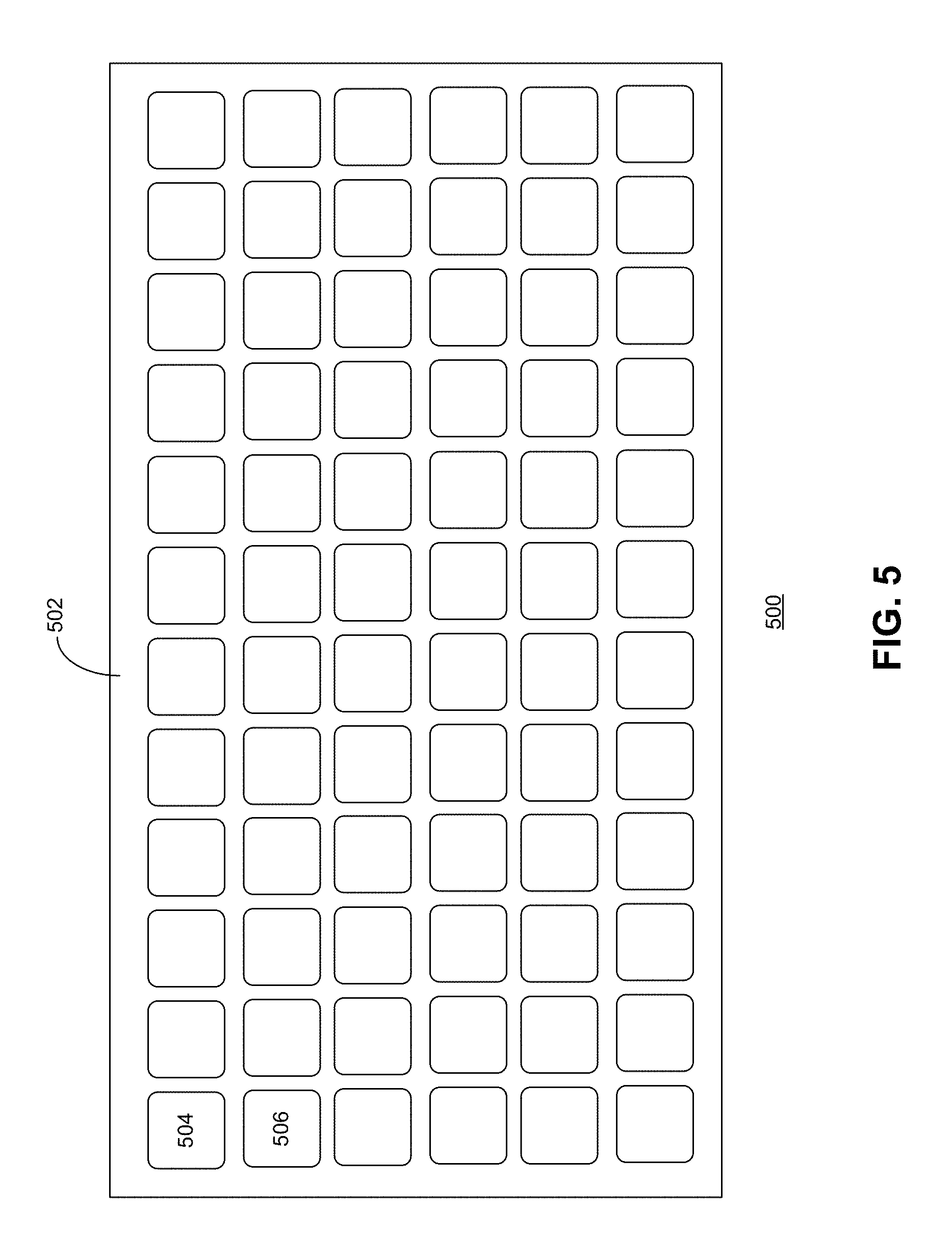
FIG. 5 shows a diagram illustrating an exemplary wafer carrier, according to an embodiment of the present invention. In FIG. 5, wafer carrier 500 includes rectangular plate 502 and a number of pockets, such as pockets 504 and 506, located on plate 502. The size of plate 502 can vary depending on the size of the deposition tool. In some embodiments, plate 502 can include 12 pockets arranged in a 3-by-4 array, thus being capable of accommodating 12 wafers. For a CVD tool with a larger chamber, plate 502 can be larger to accommodate more wafers. Large-scale batch processing is preferred in solar cell fabrications due to the reduced cost. In some embodiments, plate 502 can include up to 72 or more pockets, which may be arranged in a 6-by-12 array, as shown in FIG. 5. Although FIG. 5 shows a rectangular wafer carrier, in practice, the wafer carrier may take any shape, such as circular, oval, square, etc.
In some embodiments, plate 502 is made of graphite, and the entire surface of plate 502 is coated with a layer of pyrolytic carbon or SiC. In further embodiments, the thickness of the pyrolytic carbon or SiC coating is between 1 and 100 micrometers, preferably between 10 and 50 micrometers. The pyrolytic carbon coating on the graphite plate not only suppresses formation of carbon particles but also prevents direct contact between the Si wafers under processing and the graphite surface. As shown in FIG. 3, elimination of the Si-graphite direct contact can improve the maximum power output of the fabricated solar cells.
In some embodiments, plate 502 is made of CFC. The surface of the CFC plate is coated with pyrolytic carbon or SiC, which can effectively seal at least a portion of the pores on the surface of the CFC plate, thus reducing outgas sing from the wafer carrier.
FIG. 6 shows a diagram illustrating a cross-sectional view of an exemplary wafer carrier, according to an embodiment of the present invention. Wafer carrier plate 600 includes a number of wafer pockets, such as pocket 602. The wafer pockets are indented regions that can confine a wafer, such as c-Si substrate 604 located within pocket 602. The depth of the pockets can be between 0.1 and 1 millimeter, making them suitable for containing substrates of various thicknesses, which can range from tens to hundreds of micrometers. The size and shape of the pockets can also vary based on application, i.e., the size and shape of wafers that are under process. In some embodiments, the pockets are designed to accommodate wafers of various sizes and shapes, including but not limited to: 5-inch by 5-inch pseudo-square (square with rounded corners), 6-inch by 6-inch pseudo-square, 5-inch by 5-inch square, and 6-inch by 6-inch square. Note that to accommodate wafers of a certain shape and size, the pockets can have a similar shape and a slightly larger size. Part of the bottom surface of the pockets to be in contact with the wafer can be configured to accommodate a fat wafer, or can have a contour shape to accommodate possible wafer warping.
Although the wafer carrier is coated with a low-porosity material, any contact between the wafer and wafer carrier may still result in possible contamination. Therefore, it is preferable to limit the area of contact between the wafers and the wafer carrier. In some embodiments, the bottom of the wafer pockets can be a non-flat surface or a partially carved-out structure. For example, the bottom surface of a wafer pocket can include a number of parallel ridges. The bottom of a wafer pocket can also be configured to have a mesh or honeycomb structure, such that the wafer contact area is reduced. On the other hand, it is desirable to retain sufficient wafer contact area to ensure good electrical and thermal conductivity between the wafer and the carrier. In some embodiments, the total wafer contact area can be between 10 and 50% of the size of the wafers.
FIG. 7 shows a diagram illustrating a wafer pocket with a ridged bottom according to an embodiment of the present invention. In this example, the bottom surface of pocket 702 includes a number of ridges, such as ridges 706 and 708. The wafer contact area is now limited to the total top surface area of the ridges. For example, in FIG. 7, instead of being in contact with the entire bottom surface of pocket 702, wafer 704 is only in contact with the top surface of the ridges, such as ridges 706 and 708. In some embodiments, the total top surface area of the ridges is between 10 and 50% of the size of the wafer.
In FIG. 7, the ridges have a cross section that is square or rectangular. In general, the cross section of the ridges may have different shapes, such as a partial sphere or a trapezoid. FIG. 8 shows an exemplary cross section of a ridged-bottom wafer pocket, according to one embodiment of the present invention. In this example, wafer 802 is supported by a number of ridges. Each ridge, such as ridge 804, has a cross section that is substantially a trapezoid, which helps increase the rigidity of the wafer carrier. Furthermore, the sloped sides of each ridge (compared with vertical side wall of square or rectangular shaped ridges) may facilitate more effective coating of the wafer carrier with pyrolytic carbon or SiC. For example, if the coating is done by deposition, a sloped surface could be more susceptible to deposited material than a vertical side wall.
In some embodiments, the corners on the wafer carrier that can potentially be in direct contact with the wafer or any mechanical part can be rounded to reduce the probability of particles being released from such contact. As shown in FIG. 8, the top surface of ridge 804 can have rounded edges. In one embodiment, the radius of a rounded edge is at least 0.1 mm, preferably greater than 0.5 mm, and more preferably greater than 1 mm.
In further embodiments, the rim of a wafer pocket can have a sloped ramp to "guide" the wafer when the wafer is loaded into the pocket. FIG. 9 shows a diagram illustrating such a configuration, according to an embodiment of the present invention. In this example, wafer pocket 902 includes a sloped ramp 904 along its rim. Sloped ramp 904 guides wafer 906 to a desired position where it can be in contact with the top surface of the ridges. In addition, the edge where sloped ramp 904 joins the top surface of wafer pocket 902 is rounded to reduce possible particle release due to contact with sharp edges.
In addition to ridges, there are a variety of ways to pattern the bottom of a wafer pocket to reduce the contact area with a wafer. Such patterns of contact areas include, but are not limited to: circle, grid, mesh, hexagon, etc. FIG. 10 shows a top view of an exemplary wafer carrier with wafer-supporting pillars, according to one embodiment of the present invention. In this example, wafer carrier 1002 includes a number of wafer pockets, such as wafer pocket 1004. On the bottom of wafer pocket 1004 there are a number of support pillars, such as support pillar 1006. Each pillar has a flat top surface. Ideally, all the top surfaces of the pillars are in the same plane to ensure good contact with the wafer for thermal and electrical conductivity.
FIG. 11 shows a top view of an exemplary wafer carrier with a grid-like wafer-support structure on the bottom, according to one embodiment of the present invention. In this example, wafer carrier 1102 includes a number of wafer pockets, such as wafer pocket 1104. The bottom of wafer pocket 1104 includes a grid structure, which protrudes from the bottom surface to support the wafer. The top surface of the support structure, which is illustrated in FIG. 11 with a cross hatch pattern, presents a grid pattern. This grid structure can improve the rigidity of wafer carrier 1102 because of the increased number of vertical walls within the wafer pockets.
Note that a variety of patterns can be used to configure the bottom of a wafer pocket. FIG. 12 shows four examples of wafer pocket design, according to embodiments of the present invention. In these examples, the cross hatch patterned or gray areas are the flat top surfaces of the wafer pocket bottom, which support the wafer. In general, the bottom of a wafer pocket can have a number of recesses or protrusions with different patterns. A particular design may depend on the desired wafer contact area, structural rigidity, and weight.
It is possible to reduce the total surface area of the wafer carrier by using a partially carved-out structure as a wafer pocket. FIG. 13A shows a corner of such an exemplary wafer carrier, according to an embodiment of the present invention. In this example, wafer carrier 1302 includes a wafer pocket 1304, which has a grid wafer-support structure 1308. Note that grid wafer-structure 1308 does not have a bottom. Compared with the grid structure illustrated in FIG. 11, which has a continuous bottom, grid wafer-support structure 1308 reduces the material on the bottom of wafer pocket 1304, which reduces the total surface area of wafer carrier 1302, resulting in less potential particle contamination to the wafer. Furthermore, this carved-out structure can reduce the weight of wafer carrier 1302 without significant compromise on the rigidity of wafer carrier 1302. Note that in this example wafer pocket 1304 also has a sloped ramp 1306 along its rim, the presence of which facilitates more precise placement of the wafer in wafer pocket 1304.
In some embodiments, a wafer pocket can have most of its bottom part carved out, wherein the wafer is supported by the inner rim of the pocket. FIG. 13B shows the cross section of such an exemplary wafer pocket, according to one embodiment of the present invention. In this example, wafer pocket 1312 includes supporting rim 1314 and sloped ramp 1316. Wafer pocket does not have bottom, and the wafer is supported by supporting rim 1314, which provides a support platform along the inner rim of wafer pocket 1312. When wafer 1318 is loaded into wafer pocket 1312, wafer 1318 is guided by sloped ramp 1316, and rests upon supporting rim 1314.
In the example described above, each wafer carrier is coated with pyrolytic carbon, SiC, or a ceramic material. The coating covers every part of the wafer carrier, including the inner side walls of each wafer pocket and the wafer-supporting structure within a wafer pocket.
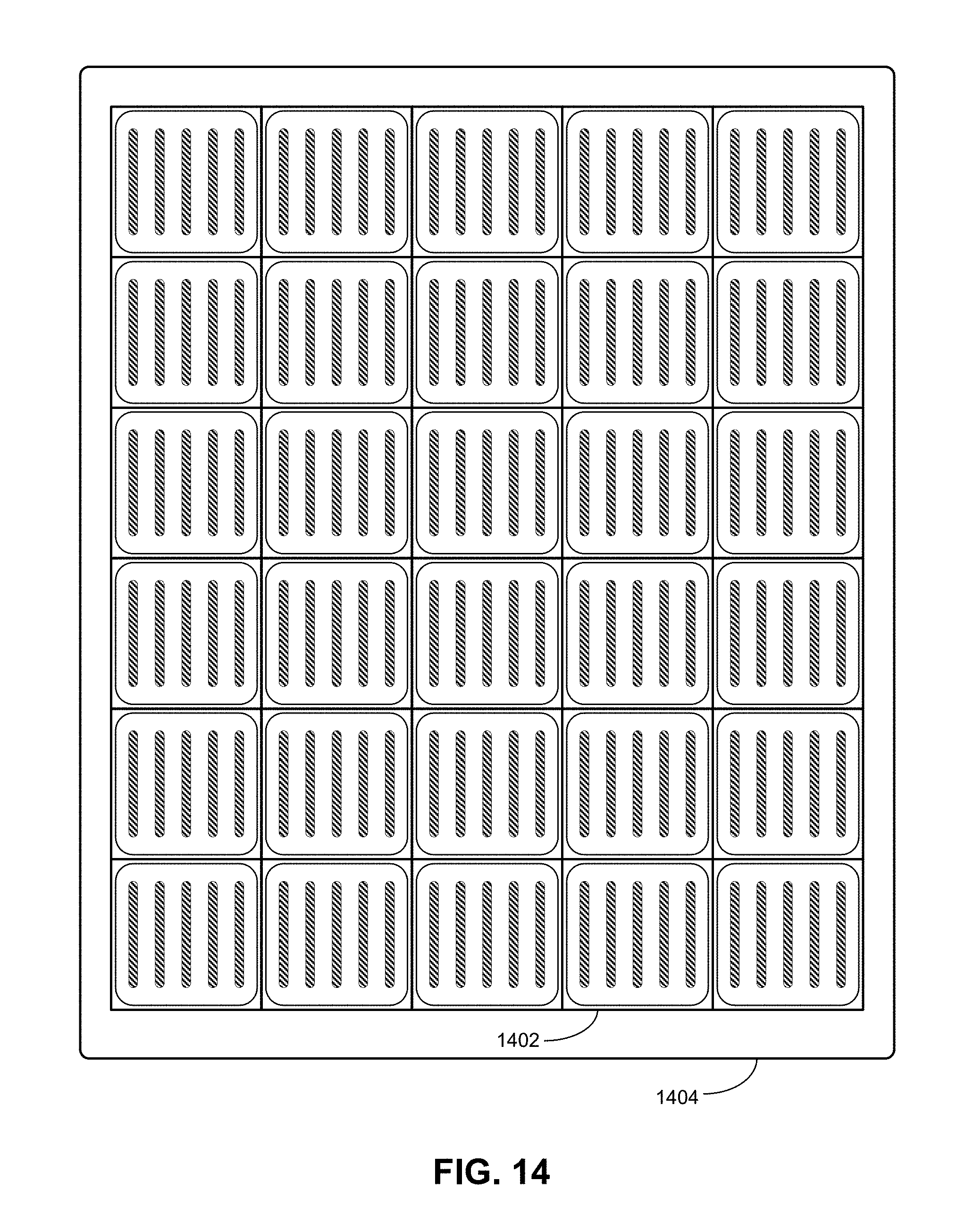
With the technological advances in wafer manufacturing it is expected that wafer sizes will continue to grow. As a result, it is expected that the dimension of wafer carriers would continue to grow. However, a wafer carrier made of carbon-based material cannot grow infinitely due to limitations in the graphite or CFC production process. To overcome this limitation, a wafer pocket can be made into an individual module, which is effectively an individual wafer carrier that can carry one wafer. Multiple such modules can be mechanically coupled together to form a larger wafer carrier.
FIG. 14 shows a top view of a wafer carrier formed by multiple modules, according to one embodiment of the present invention. In this example, a number of modules, such as module 1402, are mechanically coupled together to form a large wafer carrier. Each module includes one wafer pocket, which has a ridged bottom as illustrated in FIG. 7. A respective module has an interlocking mechanism on each of its four edges, which allows the module to be mechanically interlocked with a neighboring module. In some embodiments, the entire wafer carrier can be optionally placed on frame 1404 made of a rigid material (such as stainless steel, titanium, or non-metallic material). The use of frame 1404 can overcome the lack of rigidity caused by the mechanical coupling between the modules. Note that the use of smaller wafer pocket modules can also save the cost of manufacturing a large, monocoque wafer carrier, because the unit cost of a single-wafer module is often cheaper than the per-pocket cost of a large, monocoque carrier. Furthermore, instead of a single wafer pocket, a wafer pocket module may include a plurality of wafer pocket.
FIG. 15 shows a cross-sectional view of two interlocked wafer pocket modules, according to one embodiment of the present invention. In this example, modules 1502 and 1504 each have a ridged bottom to support wafers 1503 and 1505, respectively. Module 1502 has edge locking mechanism 1510, and module 1504 has edge locking mechanism 1508. To form a large wafer carrier, edge locking mechanisms 1510 and 1508 are mechanically coupled together. Furthermore, the entire wafer carrier system, which is formed by these interlocking modules, is placed on stainless steel frame 1512. Stainless steel frame 1512 provides the physical support for the entire wafer carrier, and prevents the interlocking mechanisms from being subject to excessive amount of mechanical stress when the wafer carrier is moved.
In some embodiments, the rigid frame that supports the entire wafer carrier can have protrusions on its bottom to facilitate placing and retaining the wafer pocket modules. FIG. 16 shows a cross-sectional view of two interlocked wafer pocket modules retained in place by a protrusion on a metal frame, according to one embodiment of the present invention. In this example, interlocked wafer pocket modules 1604 and 1606 are placed on stainless steel frame 1602. Both modules 1604 and 1606 have a recess at the location where these two modules are coupled together. Ideally, this recess matches protrusion 1608 on frame 1602. The presence of protrusion 1608 prevents wafer pocket modules 1604 and 1606 from being displaced.
Note that protrusion 1608 can be an elongated ridge along the joining seam of two interlocked modules, or can be a partial sphere at the joining point of four interlocked modules. FIG. 17 shows a top view of four interlocked wafer pocket modules retained by elongated protrusion ridges on a supporting rigid frame, according to one embodiment of the present invention. In this example, longitudinal protrusion ridge 1704 placed between columns of interlocked modules prevents the modules from being displaced in the left-right direction. Latitudinal protrusion ridge 1702 placed between rows of interlocked modules prevents the modules from being displaced in the up-down direction. FIG. 18 shows a top view of four interlocked wafer pocket modules retained by spherical protrusions on a supporting rigid frame, according to one embodiment of the present invention. In this example, spherical protrusion 1802 is placed at the location where four interlocked wafer pocket modules join. Such a protrusion is present at each of such joining locations. These protrusions can jointly prevent the interlocked modules from moving in any direction. Note that in one embodiment the recess at each corner of a wafer pocket module can be a portion of a sphere (e.g., a quarter of a semi-sphere), such that when four modules are interlocked together their respective recesses jointly form a half sphere, which can match the half-sphere protrusion on the underlying rigid frame.
FIG. 19 presents a diagram illustrating an exemplary chemical vapor deposition (CVD) tool used for solar cell fabrication, according to an embodiment of the present invention. In FIG. 19, CVD tool 1900 includes chamber 1902, top gas delivery system 1904, optional bottom gas exhaust system 1906, and wafer carrier 1908.
Chamber 1902 holds the reaction gases. The top gas delivery system 1904 and bottom gas exhaust system 1906 can deliver reaction gases into chamber 1902 and output exhaust gases from chamber 1902. The arrows show the direction of the gas flow. To ensure a uniform deposition across the wafer surface, sub-gas lines with individual flow control can be used for gas delivery. Detailed descriptions of a uniform gas delivery system can be found in U.S. patent application Ser. No. 12/952,127, entitled "Multi-Channel Gas-Delivery System," by inventors Yan Rozenzon, Robert T. Trujillo, and Steven C. Beese, filed Nov. 22, 2010, the disclosure of which is incorporated herein by reference in its entirety.
Wafer carrier 1908 is positioned inside chamber 1902. In some embodiments, wafer carrier 1908 is oriented horizontally in such a way that the to-be-deposited wafer surface is facing the incoming gas flow. In some embodiments, wafer carrier 1908 is made of graphite or CFC with its surface coated with a layer of pyrolytic carbon or SiC. In further embodiments, the thickness of the coating is between 10 and 50 micrometers. As shown in FIG. 19, wafer carrier 1908 includes a number of pockets for holding wafers. To minimize contact between wafer carrier 1908 and the wafers, in some embodiments, the bottom of the pockets can be a non-flat surface or a partially carved-out structure. Furthermore, wafer carrier 1908 can be configured based on any of the embodiments described above.
The foregoing descriptions of various embodiments have been presented only for purposes of illustration and description. They are not intended to be exhaustive or to limit the present invention to the forms disclosed. Accordingly, many modifications and variations will be apparent to practitioners skilled in the art. Additionally, the above disclosure is not intended to limit the present invention.
* * * * *
References
-
leb.eei.uni-erlangen.de/winterakademie/2010/report/course03/pdf/0306.pdf
-
-
search.credoreference.com/content/entry/hcengdict/convex/0
-
ece.uwaterloo.ca/.about.bcui/content/NE/%020343/Chapter/%207%20Dopant%20diffusion%20_%20I.pptx
-
crh.noaa.gov/lmk/?n=seasonsAccessedOct
-
-
adhesivesresearch.com/electrically-conductive-foil-tape-for-bus-bar-components-in-photovoltaic-modules
D00000
D00001
D00002
D00003
D00004
D00005
D00006
D00007
D00008
D00009
D00010
D00011
D00012

D00013

D00014

D00015

XML
uspto.report is an independent third-party trademark research tool that is not affiliated, endorsed, or sponsored by the United States Patent and Trademark Office (USPTO) or any other governmental organization. The information provided by uspto.report is based on publicly available data at the time of writing and is intended for informational purposes only.
While we strive to provide accurate and up-to-date information, we do not guarantee the accuracy, completeness, reliability, or suitability of the information displayed on this site. The use of this site is at your own risk. Any reliance you place on such information is therefore strictly at your own risk.
All official trademark data, including owner information, should be verified by visiting the official USPTO website at www.uspto.gov. This site is not intended to replace professional legal advice and should not be used as a substitute for consulting with a legal professional who is knowledgeable about trademark law.