Capacitive touch circuit pattern and manufacturing method thereof
Liu , et al.
U.S. patent number 10,282,040 [Application Number 13/256,933] was granted by the patent office on 2019-05-07 for capacitive touch circuit pattern and manufacturing method thereof. This patent grant is currently assigned to TPK Touch Solutions (Xiamen) Inc.. The grantee listed for this patent is Chen-Yu Liu, Ching-Yi Wang. Invention is credited to Chen-Yu Liu, Ching-Yi Wang.


| United States Patent | 10,282,040 |
| Liu , et al. | May 7, 2019 |
Capacitive touch circuit pattern and manufacturing method thereof
Abstract
The present disclosure relates to a touch circuit pattern and a manufacturing method thereof. A capacitive touch circuit pattern in the present disclosure comprises a substrate, wherein at least two adjacent transparent first-axis electrode blocks, a transparent first-axis conductive wire, and at least two adjacent transparent second-axis electrode blocks are formed on the substrate. The first-axis conductive wire is formed between the two adjacent first-axis electrode blocks to connect the two adjacent first-axis electrode blocks and the two adjacent second-axis electrode blocks, respectively, at two sides of the first-axis conductive wire. The capacitive touch circuit pattern further comprises of a metal second-axis conductive wire, which stretches across the first-axis conductive wire and connects the two adjacent second-axis electrode blocks.
| Inventors: | Liu; Chen-Yu (Jhongli, CN), Wang; Ching-Yi (Zhongli, CN) | ||||||||||
|---|---|---|---|---|---|---|---|---|---|---|---|
| Applicant: |
|
||||||||||
| Assignee: | TPK Touch Solutions (Xiamen)
Inc. (Xiamen, CN) |
||||||||||
| Family ID: | 42739174 | ||||||||||
| Appl. No.: | 13/256,933 | ||||||||||
| Filed: | March 19, 2010 | ||||||||||
| PCT Filed: | March 19, 2010 | ||||||||||
| PCT No.: | PCT/CN2010/000334 | ||||||||||
| 371(c)(1),(2),(4) Date: | October 17, 2011 | ||||||||||
| PCT Pub. No.: | WO2010/105507 | ||||||||||
| PCT Pub. Date: | September 23, 2010 |
Prior Publication Data
| Document Identifier | Publication Date | |
|---|---|---|
| US 20120127099 A1 | May 24, 2012 | |
Foreign Application Priority Data
| Mar 20, 2009 [CN] | 2009 1 0129503 | |||
| Mar 20, 2009 [CN] | 2009 2 0006657 U | |||
| Current U.S. Class: | 1/1 |
| Current CPC Class: | G06F 3/044 (20130101); G06F 3/0446 (20190501); G06F 2203/04111 (20130101); Y10T 29/49105 (20150115) |
| Current International Class: | G06F 3/044 (20060101) |
| Field of Search: | ;345/173,174,156,157 |
References Cited [Referenced By]
U.S. Patent Documents
| 4028509 | June 1977 | Zurcher |
| 4233522 | November 1980 | Chalmers Ma et al. |
| 4550221 | October 1985 | Mabusth |
| 4733222 | March 1988 | Evans |
| 5374787 | December 1994 | Miller et al. |
| 5381160 | January 1995 | Landmeier |
| 5495077 | February 1996 | Miller et al. |
| 5543590 | August 1996 | Gillespie et al. |
| 5648642 | July 1997 | Miller et al. |
| 5844506 | December 1998 | Binstead et al. |
| 5880411 | March 1999 | Gillespie et al. |
| 6005555 | December 1999 | Katsurahira et al. |
| 6114862 | September 2000 | Tartagni et al. |
| 6137427 | October 2000 | Binstead et al. |
| 6177918 | January 2001 | Colgan et al. |
| 6188391 | February 2001 | Seely et al. |
| 6239389 | May 2001 | Allen et al. |
| 6392636 | May 2002 | Ferrari et al. |
| 6414671 | July 2002 | Gillespie et al. |
| 6496021 | December 2002 | Tartagni et al. |
| 6498590 | December 2002 | Dietz et al. |
| 6664489 | December 2003 | Kleinhans et al. |
| 6740945 | May 2004 | Lepert et al. |
| 6924789 | August 2005 | Bick et al. |
| 6970160 | November 2005 | Mulligan et al. |
| 7030860 | April 2006 | Hsu et al. |
| 7202859 | April 2007 | Speck et al. |
| 7292229 | November 2007 | Morag et al. |
| 7382139 | June 2008 | Mackey |
| 7439962 | October 2008 | Reynolds et al. |
| 7463246 | December 2008 | Mackey et al. |
| 7477242 | January 2009 | Cross et al. |
| 7532205 | May 2009 | Gillespie et al. |
| 7589713 | September 2009 | Sato |
| 7663607 | February 2010 | Hotelling et al. |
| 7671847 | March 2010 | Weng |
| 7821502 | October 2010 | Hristov |
| 7864160 | January 2011 | Geaghan et al. |
| 7952564 | May 2011 | Hurst et al. |
| 8004497 | August 2011 | XiaoPing |
| 8040321 | October 2011 | Peng et al. |
| 8058937 | November 2011 | Qin et al. |
| 8059015 | November 2011 | Hua et al. |
| 8068097 | November 2011 | GuangHai |
| 8068186 | November 2011 | Aufderheide et al. |
| 8072429 | December 2011 | Grivna |
| 8085250 | December 2011 | Reynolds et al. |
| 8111243 | February 2012 | Peng et al. |
| 8120584 | February 2012 | Grivna et al. |
| 8144125 | March 2012 | Peng et al. |
| 8169421 | May 2012 | Wright et al. |
| 8217902 | July 2012 | Chang et al. |
| 2003/0048261 | March 2003 | Yamamoto et al. |
| 2003/0234770 | December 2003 | MacKey |
| 2004/0119701 | June 2004 | Mulligan et al. |
| 2004/0178997 | September 2004 | Gillespie et al. |
| 2005/0030048 | February 2005 | Bolender et al. |
| 2006/0066581 | March 2006 | Lyon et al. |
| 2006/0097991 | May 2006 | Hotelling et al. |
| 2006/0274055 | December 2006 | Reynolds et al. |
| 2007/0046648 | March 2007 | Lee et al. |
| 2007/0132737 | June 2007 | Mulligan et al. |
| 2007/0229469 | October 2007 | Seguine et al. |
| 2007/0229470 | October 2007 | Snyder et al. |
| 2007/0236618 | October 2007 | Maag et al. |
| 2007/0240914 | October 2007 | Lai et al. |
| 2007/0242054 | October 2007 | Chang et al. |
| 2007/0273672 | November 2007 | Hong et al. |
| 2008/0036473 | February 2008 | Jansson et al. |
| 2008/0074398 | March 2008 | Wright et al. |
| 2008/0150906 | June 2008 | Grivna et al. |
| 2008/0180399 | July 2008 | Cheng et al. |
| 2008/0231605 | September 2008 | Yang et al. |
| 2008/0264699 | October 2008 | Chang et al. |
| 2008/0314626 | December 2008 | Moore |
| 2009/0160682 | June 2009 | Bolender et al. |
| 2009/0160824 | June 2009 | Chih-Yung et al. |
| 2009/0277695 | November 2009 | Liu et al. |
| 2010/0007616 | January 2010 | Jang |
| 2010/0045614 | February 2010 | Gray et al. |
| 2010/0073310 | March 2010 | Liang et al. |
| 2010/0073319 | March 2010 | Lyon et al. |
| 2010/0079384 | April 2010 | Grivna |
| 2010/0156810 | June 2010 | Barbier et al. |
| 2010/0253645 | October 2010 | Bolender |
| 2011/0141038 | June 2011 | Kuo et al. |
| 2012/0068968 | March 2012 | Reynolds et al. |
| 1754141 | Mar 2006 | CN | |||
| 1818842 | Aug 2006 | CN | |||
| 101131492 | Feb 2008 | CN | |||
| 201078769 | Jun 2008 | CN | |||
| 101261379 | Sep 2008 | CN | |||
| 101324827 | Dec 2008 | CN | |||
| 101349960 | Jan 2009 | CN | |||
| 101359265 | Feb 2009 | CN | |||
| 101441545 | May 2009 | CN | |||
| 201298221 | Aug 2009 | CN | |||
| 101587391 | Nov 2009 | CN | |||
| 201374687 | Dec 2009 | CN | |||
| 2290512 | Mar 2011 | EP | |||
| 2168816 | Jun 1986 | GB | |||
| 57204938 | Dec 1982 | JP | |||
| 58166437 | Jan 1983 | JP | |||
| 60075927 | Apr 1985 | JP | |||
| 6184729 | Apr 1986 | JP | |||
| 2002252340 | Sep 2002 | JP | |||
| 2008310551 | Dec 2008 | JP | |||
| 3149113 | Feb 2009 | JP | |||
| 2010033478 | Feb 2010 | JP | |||
| 2010160670 | Jul 2010 | JP | |||
| 2011070659 | Apr 2011 | JP | |||
| 2011198339 | Oct 2011 | JP | |||
| 2011198839 | Oct 2011 | JP | |||
| 2012094147 | May 2012 | JP | |||
| 20070102414 | Oct 2007 | KR | |||
| 1020070102414 | Oct 2007 | KR | |||
| 1020080096352 | Oct 2007 | KR | |||
| 101040881 | Jun 2011 | KR | |||
| 101073333 | Oct 2011 | KR | |||
| M342558 | Oct 2008 | TW | |||
| 345294 | Nov 2008 | TW | |||
| 200842681 | Nov 2008 | TW | |||
| 200842681 | Nov 2008 | TW | |||
| M423866 | Mar 2012 | TW | |||
| 2010029979 | Mar 2010 | WO | |||
Assistant Examiner: Parker; Jeffrey
Attorney, Agent or Firm: Cooper Legal Group, LLC
Claims
What is claimed is:
1. A method of manufacturing a capacitive touch circuit pattern, comprising: simultaneously forming two adjacent transparent first-axis electrode blocks, a transparent first-axis conductive wire, and two adjacent transparent second-axis electrode blocks on a surface of a substrate through a first process, wherein: the transparent first-axis conductive wire is disposed between the two adjacent transparent first-axis electrode blocks to connect the two adjacent transparent first-axis electrode blocks, and the two adjacent transparent second-axis electrode blocks are disposed on opposite sides of the transparent first-axis conductive wire; forming an insulation layer only on a surface of the transparent first-axis conductive wire through a second process, wherein the two adjacent transparent second-axis electrode blocks are exposed from the insulation layer, and the two adjacent transparent first-axis electrode blocks are exposed from the insulation layer; and simultaneously forming a first-axis surrounding circuit, a second-axis surrounding circuit and a metal second-axis conductive wire through a third process, wherein: the metal second-axis conductive wire is directly formed on the two adjacent transparent second-axis electrode blocks, the metal second-axis conductive wire extends across a first transparent second-axis electrode block of the two adjacent transparent second-axis electrode blocks from a first end of the first transparent second-axis electrode block facing the transparent first-axis conductive wire to a second end of the first transparent second-axis electrode block diametrically opposite the first end, a part of the metal second-axis conductive wire crosses the insulating layer, and the metal second-axis conductive wire and the second-axis surrounding circuit are integrally formed as a T-shaped structure; and wherein a surface of either one of the two adjacent transparent second-axis electrode blocks, that are exposed from the insulation layer, comprises a first surface portion exposed from the metal second-axis conductive wire, a second surface portion covered by the metal second-axis conductive wire, and a third surface portion exposed from the metal second-axis conductive wire, and wherein the first surface portion and the third surface portion are formed on opposite sides of the second surface portion.
2. The method of manufacturing a capacitive touch circuit pattern as claimed in claim 1, wherein: the first-axis surrounding circuit is formed at a first edge of the substrate and the second-axis surrounding circuit is formed at a second edge of the substrate that is adjacent to the first edge, and the two adjacent transparent first-axis electrode blocks connect to the first-axis surrounding circuit and the two adjacent transparent second-axis electrode blocks connect to the second-axis surrounding circuit.
3. The method of manufacturing a capacitive touch circuit pattern as claimed in claim 1, wherein the metal second-axis conductive wire extends continuously from the first end of the first transparent second-axis electrode block to the second end of the first transparent second-axis electrode block.
4. The method of manufacturing a capacitive touch circuit pattern as claimed in claim 1, wherein a longest dimension of the second-axis surrounding circuit extends in a first direction and a longest dimension of the metal second-axis conductive wire extends in a second direction perpendicular to the first direction.
5. The method of manufacturing a capacitive touch circuit pattern as claimed in claim 1, wherein the substrate is made of glass or plastic, and wherein the first-axis surrounding circuit, the second-axis surrounding circuit and the metal second-axis conductive wire are made of gold, silver, copper, or aluminum.
6. A capacitive touch circuit pattern structure, comprising: two adjacent transparent first-axis electrode blocks; a transparent first-axis conductive wire; two adjacent transparent second-axis electrode blocks, wherein: the two adjacent transparent first-axis electrode blocks, the transparent first-axis conductive wire, and the two adjacent transparent second-axis electrode blocks are simultaneously formed on a substrate, the transparent first-axis conductive wire is formed between the two adjacent transparent first-axis electrode blocks to connect the two adjacent transparent first-axis electrode blocks, and the two adjacent transparent second-axis electrode blocks are disposed on opposite sides of the transparent first-axis conductive wire; a first-axis surrounding circuit; a second-axis surrounding circuit; a metal second-axis conductive wire, wherein: the first-axis surrounding circuit, the second-axis surrounding circuit and the metal second-axis conductive wire are simultaneously formed, and the metal second-axis conductive wire connects the two adjacent transparent second-axis electrode blocks; and an insulation spacer only formed on a surface of the transparent first-axis conductive wire, and formed between the transparent first-axis conductive wire and the metal second-axis conductive wire to electrically insulate the transparent first-axis conductive wire from the metal second-axis conductive wire, wherein: the two adjacent transparent second-axis electrode blocks are exposed from the insulation spacer, and the two adjacent transparent first-axis electrode blocks are exposed from the insulation spacer, the metal second-axis conductive wire is directly formed on the two adjacent transparent second-axis electrode blocks, the metal second-axis conductive wire extends across a first transparent second-axis electrode block of the two adjacent transparent second-axis electrode blocks from a first end of the first transparent second-axis electrode block facing the transparent first-axis conductive wire to a second end of the first transparent second-axis electrode block diametrically opposite the first end, a part of the metal second-axis conductive wire crosses the insulation spacer, and the metal second-axis conductive wire and the second-axis surrounding circuit are integrally formed as a T-shaped structure; and wherein a surface of either one of the two adjacent transparent second-axis electrode blocks, that are exposed from the insulation spacer, comprises a first surface portion exposed from the metal second-axis conductive wire, a second surface portion covered by the metal second-axis conductive wire, and a third surface portion exposed from the metal second-axis conductive wire, and wherein the first surface portion and the third surface portion are formed on opposite sides of the second surface portion.
7. The capacitive touch circuit pattern structure as claimed in claim 6, wherein: the first-axis surrounding circuit and the second-axis surrounding circuit are formed at edges of the substrate, the first-axis surrounding circuit connects to the two adjacent transparent first-axis electrode blocks, and the second-axis surrounding circuit connects to the two adjacent transparent second-axis electrode blocks.
8. The capacitive touch circuit pattern structure as claimed in claim 6, wherein the metal second-axis conductive wire extends continuously from the first end of the first transparent second-axis electrode block to the second end of the first transparent second-axis electrode block.
9. The capacitive touch circuit pattern structure as claimed in claim 6, further comprising a third transparent second-axis electrode block adjacent one of the two adjacent transparent second-axis electrode blocks, wherein the metal second-axis conductive wire extends continuously across the two adjacent transparent second-axis electrode blocks and the third transparent second-axis electrode block.
10. The capacitive touch circuit pattern structure as claimed in claim 6, wherein a longest dimension of the second-axis surrounding circuit extends in a first direction and a longest dimension of the metal second-axis conductive wire extends in a second direction perpendicular to the first direction.
11. The capacitive touch circuit pattern structure as claimed in claim 6, wherein the substrate is made of glass or plastic, and wherein the first-axis surrounding circuit, the second-axis surrounding circuit and the metal second-axis conductive wire are made of gold, silver, copper, or aluminum.
12. A touch display screen, comprising: a display panel, comprising an upper substrate, a lower substrate, and a pixel unit disposed between the upper substrate and the lower substrate; and a capacitive touch circuit pattern structure applied to one of the upper substrate or the lower substrate, wherein the capacitive touch circuit pattern structure comprises: two adjacent transparent first-axis electrode blocks disposed on the one of the upper substrate or the lower substrate; a transparent first-axis conductive wire disposed on the one of the upper substrate or the lower substrate; two adjacent transparent second-axis electrode blocks disposed on the one of the upper substrate or the lower substrate, wherein: the transparent first-axis conductive wire is formed between the two adjacent transparent first-axis electrode blocks to connect the two adjacent transparent first-axis electrode blocks, and the two adjacent transparent second-axis electrode blocks are disposed on opposite sides of the transparent first-axis conductive wire; a second-axis surrounding circuit; a second-axis conductive wire, wherein the second-axis conductive wire connects the two adjacent transparent second-axis electrode blocks; and an insulation spacer only formed on a surface of the transparent first-axis conductive wire, and formed between the transparent first-axis conductive wire and the second-axis conductive wire to electrically insulate the transparent first-axis conductive wire from the second-axis conductive wire, wherein: the two adjacent transparent second-axis electrode blocks are exposed from the insulation spacer, and the two adjacent transparent first-axis electrode blocks are exposed from the insulation spacer, the second-axis conductive wire contact the two adjacent transparent second-axis electrode blocks, the second-axis conductive wire extends across a first transparent second-axis electrode block of the two adjacent transparent second-axis electrode blocks from a first end of the first transparent second-axis electrode block facing the transparent first-axis conductive wire to a second end of the first transparent second-axis electrode block diametrically opposite the first end, a part of the second-axis conductive wire crosses the insulation spacer, and the second-axis conductive wire and the second-axis surrounding circuit are integrally formed as a T-shaped structure; and wherein a surface of either one of the two adjacent transparent second-axis electrode blocks, that are exposed from the insulation spacer, comprises a first surface portion exposed from the second-axis conductive wire, a second surface portion covered by the second-axis conductive wire, and a third surface portion exposed from the second-axis conductive wire, and wherein the first surface portion and the third surface portion are formed on opposite sides of the second surface portion.
13. The touch display screen as claimed in claim 12, wherein the second-axis conductive wire is made of a non-transparent conductive material.
14. The touch display screen as claimed in claim 13, wherein: the capacitive touch circuit pattern structure is disposed between the upper substrate and the lower substrate, and the second-axis conductive wire is disposed as a shading element in the display panel.
15. The touch display screen as claimed in claim 12, wherein: the display panel further comprises a black matrix, and the second-axis conductive wire is aligned with the black matrix.
16. The touch display screen as claimed in claim 12, wherein the second-axis conductive wire is metal.
17. The touch display screen as claimed in claim 12, wherein the two adjacent transparent first-axis electrode blocks, the transparent first-axis conductive wire, and the two adjacent transparent second-axis electrode blocks are simultaneously formed on the one of the upper substrate or the lower substrate.
18. The touch display screen as claimed in claim 12, further comprising a first-axis surrounding circuit, wherein the first-axis surrounding circuit, the second-axis surrounding circuit and the second-axis conductive wire are simultaneously formed.
19. The touch display screen as claimed in claim 18, wherein the upper substrate or the lower substrate is made of glass or plastic, and wherein the first-axis surrounding circuit, the second-axis surrounding circuit and the second-axis conductive wire are made of gold, silver, copper, or aluminum.
20. The touch display screen as claimed in claim 12, wherein the second-axis conductive wire extends continuously from the first end of the first transparent second-axis electrode block to the second end of the first transparent second-axis electrode block.
21. The touch display screen as claimed in claim 12, wherein a longest dimension of the second-axis surrounding circuit extends in a first direction and a longest dimension of the second-axis conductive wire extends in a second direction perpendicular to the first direction.
22. A method of manufacturing a capacitive touch circuit pattern, comprising: simultaneously forming two adjacent transparent first-axis electrode blocks, a transparent first-axis conductive wire, and two adjacent transparent second-axis electrode blocks on a surface of a substrate through a first process, wherein: the transparent first-axis conductive wire is disposed between the two adjacent transparent first-axis electrode blocks to connect the two adjacent transparent first-axis electrode blocks, and the two adjacent transparent second-axis electrode blocks are disposed on opposite sides of the transparent first-axis conductive wire; forming an insulation layer only on a surface of the transparent first-axis conductive wire through a second process, wherein the two adjacent transparent first-axis electrode blocks are exposed from the insulation layer, and the two adjacent transparent second-axis electrode blocks are exposed from the insulation layer; and simultaneously forming a first-axis surrounding circuit, a second-axis surrounding circuit and a second-axis conductive wire through a third process, wherein: the second-axis conductive wire is directly formed on the two adjacent transparent second-axis electrode blocks, the second-axis conductive wire extends across a first transparent second-axis electrode block of the two adjacent transparent second-axis electrode blocks from a first end of the first transparent second-axis electrode block facing the transparent first-axis conductive wire to a second end of the first transparent second-axis electrode block diametrically opposite the first end, and a part of the second-axis conductive wire crosses the insulating layer; and wherein a surface of either one of the two adjacent transparent second-axis electrode blocks, that are exposed from the insulation layer, comprises a first surface portion exposed from the second-axis conductive wire, a second surface portion covered by the second-axis conductive wire, and a third surface portion exposed from the second-axis conductive wire, and wherein the first surface portion and the third surface portion are formed on opposite sides of the second surface portion.
23. The method of manufacturing a capacitive touch circuit pattern as claimed in claim 22, wherein the second-axis conductive wire and the second-axis surrounding circuit are integrally formed as a T-shaped structure.
24. The method of manufacturing a capacitive touch circuit pattern as claimed in claim 23, wherein a longest dimension of the second-axis surrounding circuit extends in a first direction and a longest dimension of the second-axis conductive wire extends in a second direction perpendicular to the first direction.
25. The method of manufacturing a capacitive touch circuit pattern as claimed in claim 24, wherein the two adjacent transparent first-axis electrode blocks are arranged along the first direction and the two adjacent transparent second-axis electrode blocks are arranged along the second direction.
26. The method of manufacturing a capacitive touch circuit pattern as claimed in claim 22, wherein the second-axis conductive wire is metal.
27. The method of manufacturing a capacitive touch circuit pattern as claimed in claim 22, wherein: the first-axis surrounding circuit and the second-axis surrounding circuit are formed at edges of the substrate, the first-axis surrounding circuit connects to the two adjacent transparent first-axis electrode blocks, and the second-axis surrounding circuit connects to the two adjacent transparent second-axis electrode blocks.
28. The method of manufacturing a capacitive touch circuit pattern as claimed in claim 22, wherein the second-axis conductive wire, the first-axis surrounding circuit and the second-axis surrounding circuit are made of a non-transparent conductive material.
29. The method of manufacturing a capacitive touch circuit pattern as claimed in claim 28, wherein the non-transparent conductive material is a metal.
30. The method of manufacturing a capacitive touch circuit pattern as claimed in claim 22, wherein the second-axis conductive wire extends continuously from the first end of the first transparent second-axis electrode block to the second end of the first transparent second-axis electrode block.
31. The method of manufacturing a capacitive touch circuit pattern as claimed in claim 22, wherein the substrate is made of glass or plastic, and wherein the first-axis surrounding circuit, the second-axis surrounding circuit and the second-axis conductive wire are made of gold, silver, copper, or aluminum.
32. A capacitive touch circuit pattern structure, comprising: two adjacent transparent first-axis electrode blocks; a transparent first-axis conductive wire; two adjacent transparent second-axis electrode blocks, wherein: the transparent first-axis conductive wire is disposed between the two adjacent transparent first-axis electrode blocks to connect the two adjacent transparent first-axis electrode blocks, and the two adjacent transparent second-axis electrode blocks are disposed on opposite sides of the transparent first-axis conductive wire; a second-axis conductive wire, wherein the second-axis conductive wire connects the two adjacent transparent second-axis electrode blocks; an insulation spacer only disposed on a surface of the transparent first-axis conductive wire, and disposed between the transparent first-axis conductive wire and the second-axis conductive wire to electrically insulate the transparent first-axis conductive wire from the second-axis conductive wire, wherein the second-axis conductive wire extends across a first transparent second-axis electrode block of the two adjacent transparent second-axis electrode blocks from a first end of the first transparent second-axis electrode block facing the transparent first-axis conductive wire to a second end of the first transparent second-axis electrode block diametrically opposite the first end, and wherein the two adjacent transparent first-axis electrode blocks are exposed from the insulation spacer, and the two adjacent transparent second-axis electrode blocks are exposed from the insulation spacer; and a second-axis surrounding circuit, wherein the second-axis conductive wire and the second-axis surrounding circuit are integrally formed as a T-shaped structure; and wherein a surface of either one of the two adjacent transparent second-axis electrode blocks, that are exposed from the insulation spacer, comprises a first surface portion exposed from the second-axis conductive wire, a second surface portion covered by the second-axis conductive wire, and a third surface portion exposed from the second-axis conductive wire, and wherein the first surface portion and the third surface portion are formed on opposite sides of the second surface portion.
33. The capacitive touch circuit pattern structure as claimed in claim 32, wherein a part of the second-axis conductive wire crosses the insulation spacer.
34. The capacitive touch circuit pattern structure as claimed in claim 32, wherein a longest dimension of the second-axis surrounding circuit extends in a first direction and a longest dimension of the second-axis conductive wire extends in a second direction perpendicular to the first direction.
35. The capacitive touch circuit pattern structure as claimed in claim 34, wherein the two adjacent transparent first-axis electrode blocks are arranged along the first direction and the two adjacent transparent second-axis electrode blocks are arranged along the second direction.
36. The capacitive touch circuit pattern structure as claimed in claim 32, wherein the two adjacent transparent first-axis electrode blocks, the transparent first-axis conductive wire, and the two adjacent transparent second-axis electrode blocks are simultaneously formed on a substrate.
37. The capacitive touch circuit pattern structure as claimed in claim 32, wherein the second-axis conductive wire is metal.
38. The capacitive touch circuit pattern structure as claimed in claim 32, further comprising a first-axis surrounding circuit, wherein the first-axis surrounding circuit, the second-axis surrounding circuit and the second-axis conductive wire are simultaneously formed on a substrate.
39. The capacitive touch circuit pattern structure as claimed in claim 38, wherein the substrate is made of glass or plastic, and wherein the first-axis surrounding circuit, the second-axis surrounding circuit and the second-axis conductive wire are made of gold, silver, copper, or aluminum.
40. The capacitive touch circuit pattern structure as claimed in claim 32, wherein the second-axis conductive wire is directly formed on the two adjacent transparent second-axis electrode blocks.
41. The capacitive touch circuit pattern structure as claimed in claim 32, wherein the second-axis conductive wire is made of a non-transparent conductive material.
42. The capacitive touch circuit pattern structure as claimed in claim 32, further comprising a first-axis surrounding circuit, wherein: the first-axis surrounding circuit is electrically connected to the two adjacent transparent first-axis electrode blocks, and the second-axis surrounding circuit is electrically connected to the two adjacent transparent second-axis electrode blocks.
43. The capacitive touch circuit pattern structure as claimed in claim 42, wherein the first-axis surrounding circuit and the second-axis surrounding circuit are made of a non-transparent conductive material.
44. The capacitive touch circuit pattern structure as claimed in claim 32, wherein the second-axis conductive wire extends continuously from the first end of the first transparent second-axis electrode block to the second end of the first transparent second-axis electrode block.
Description
FIELD OF THE INVENTION
The present disclosure relates to a touch circuit pattern and a manufacturing method thereof, and more particularly to a capacitive touch circuit pattern formed on surface of a transparent substrate and a disposition technology thereof.
BACKGROUND OF THE INVENTION
Conventional touch input modes of touch panels comprise of resistive mode, capacitive mode, optical mode, electromagnetic induction mode, and acoustic wave sensing mode, etc. For the resistive mode and capacitive mode, a user touches the surface of a panel by a finger or a stylus, causing a change of voltage and current inside touch location of the panel, and then the touch location on surface of the panel can be detected so to achieve the purpose of a touch input.
In order to detect a location on a touch panel touched by a user with a finger or a stylus, those skilled in the art have developed various capacitive touch sensing technologies. For example, structure of a grid capacitive touch circuit pattern comprises two groups of capacitive sensing layers which are spaced by an intermediate insulation layer so as to form capacitance effect. Each capacitive sensing layer comprises conductive elements which are arranged substantially parallel to each other. The two capacitive sensing layers are substantially perpendicular to each other; each conductive element comprising a series of diamond-shaped electrode blocks. The conductive element is made of a transparent conductive material (such as ITO), and the electrode blocks are connected by narrow conductive wires. Conductive elements on each capacitive sensing layer are electrically connected to a surrounding circuit. A control circuit provides signals to two groups of conductive elements respectively, via the surrounding circuits and can receive touch signals generated by electrode blocks when a surface is touched so as to determine the touch location on each layer.
Moreover, the method of manufacturing a conventional capacitive touch circuit pattern structure includes forming a plurality of electrode blocks of a first group of capacitive sensing layer through the first processing. A surrounding circuit is formed through a second process such that the surrounding circuit is connected to the electrode blocks of the first group of capacitive sensing layer, to form a whole insulation layer through a third process. A plurality of electrode blocks of a second group of capacitive sensing layer are formed through a fourth process and another surrounding circuit is formed through a fifth process. Finally the surrounding circuit is connected to the electrode blocks of the second group of the capacitive sensing layer. The shortcoming in this procedure is that for making the electrode blocks of the two groups of the capacitive sensing layers, the insulation layer and the two groups of surrounding circuits must be formed through the above disclosed five processing steps, which makes the overall process very complex. Conductive wires used for connecting the electrode blocks are made of ITO, which further makes it difficult to effectively reduce the impedance between the electrode blocks and the surrounding circuits.
Thus, there exists a need to improve sensitivity of signal transmission between the electrode blocks and the surrounding circuits.
SUMMARY OF THE INVENTION
An object of the present disclosure is to provide a capacitive touch circuit pattern and a manufacturing method for completing formation of electrode blocks along two axial directions together through a single process so as to simplify the process of disposing the touch circuit pattern.
In another embodiment, a capacitive touch circuit pattern in the present disclosure comprises: a substrate, wherein at least two adjacent transparent first-axis electrode blocks, a transparent first-axis conductive wire and at least two adjacent transparent second-axis electrode blocks are formed on the substrate; wherein the first-axis conductive wire is formed between the two adjacent first-axis electrode blocks to connect the two adjacent first-axis electrode blocks and the two adjacent second-axis electrode blocks, respectively, at two sides of the first-axis conductive wire; a metal second-axis conductive wire, which stretches across the first-axis conductive wire and connects the two adjacent second-axis electrode blocks; an insulation spacer, which is formed between the first-axis conductive wire and the second-axis conductive wire such that the first-axis conductive wire and the second-axis conductive wire are electrically insulated; wherein a first-axis surrounding circuit and a second-axis surrounding circuit are, respectively, formed at two adjacent edges of the substrate, the first-axis surrounding circuit connecting the first-axis electrode blocks and the second-axis surrounding circuit connecting the second-axis electrode blocks.
The present disclosure also provides a method of manufacturing a capacitive touch circuit pattern comprising of: forming two adjacent first-axis electrode blocks, a first-axis conductive wire and two adjacent second-axis electrode blocks on surface of a substrate through a first process; wherein the first-axis conductive wire is disposed between the two adjacent first-axis electrode blocks to connect the two adjacent first-axis electrode blocks; wherein the two adjacent second-axis electrode blocks are disposed, respectively, at two sides of the first-axis conductive wire; forming an insulation layer on the surface of the substrate to cover the first-axis conductive wire through a second process; forming a metal second-axis conductive wire on the insulation layer to connect the two adjacent second-axis electrode blocks through a third process such that the first-axis conductive wire and the second-axis conductive wire are electrically insulated and thus a touch circuit pattern is formed.
The method further comprises forming a first-axis surrounding circuit and a second-axis surrounding circuit, respectively, at two adjacent edges of the substrate at the same time when forming the second-axis conductive wire so that the first-axis surrounding circuit connects the first-axis electrode blocks and the second-axis surrounding circuit connects the second-axis electrode blocks.
The insulation layer is an insulation spacer and the second-axis conductive wire stretches across the insulation spacer. The insulation layer can also cover the two adjacent first-axis electrode blocks and the two adjacent second-axis electrode blocks. There are two adjacent through-holes on the surface of the insulation layer, which are respectively formed above the two adjacent second-axis electrode blocks. The second-axis conductive wire is located between the two adjacent through-holes and is superposed on the two adjacent through-holes to connect the two adjacent second-axis electrode blocks.
Another method of manufacturing a capacitive touch circuit pattern comprises: forming a metal second-axis conductive wire on surface of a substrate through a first process; forming an insulation layer on the surface of the substrate to cover the second-axis conductive wire through a second process; forming two adjacent first-axis electrode blocks, a first-axis conductive wire, and two adjacent second-axis electrode blocks on the substrate through a third process; wherein the two adjacent second-axis electrode blocks respectively connect to two ends of the second-axis conductive wire; wherein the two adjacent first-axis electrode blocks are disposed respectively at two sides of the second-axis conductive wire; wherein the first-axis conductive wire is located on the insulation layer and connects the two adjacent first-axis electrode blocks so that the first-axis conductive wire and the second-axis conductive wire are electrically insulated to form a touch circuit pattern.
The method further comprises forming a first-axis surrounding circuit and a second-axis surrounding circuit, respectively, at two adjacent edges of the substrate at the same time when forming the second-axis conductive wire so that the first-axis electrode blocks connect the first-axis surrounding circuit and the second-axis electrode blocks connect the second-axis surrounding circuit.
The insulation layer is an insulation spacer and the first-axis conductive wire stretches across the insulation spacer. There are two adjacent through-holes on the surface of the insulation layer, which are respectively formed above the two ends of the second-axis conductive wire. The two adjacent first-axis electrode blocks and the two adjacent second-axis electrode blocks are located on the insulation layer, and the two adjacent second-axis electrode blocks are superposed on the through-holes to connect the two ends of the second-axis conductive wire, respectively.
In order to achieve the purpose, the present disclosure also provides a capacitive touch circuit pattern structure, which comprises: a substrate, wherein at least two adjacent transparent first-axis electrode blocks, a transparent first-axis conductive wire and at least two adjacent transparent second-axis electrode blocks are formed on the substrate. The first-axis conductive wire is formed between the two adjacent first-axis electrode blocks to connect the two adjacent first-axis electrode blocks. The two adjacent second-axis electrode blocks are disposed at two sides of the first-axis conductive wire; a metal second-axis conductive wire, which stretches across the first-axis conductive wire and connects the two adjacent second-axis electrode blocks An insulation spacer is formed between the first-axis conductive wire and the second-axis conductive wire such that the first-axis conductive wire and the second-axis conductive wire are electrically insulated.
Further, a first-axis surrounding circuit and a second-axis surrounding circuit are respectively, formed at two adjacent edges of the substrate, the first-axis surrounding circuit connecting the first-axis electrode blocks and the second-axis surrounding circuit connecting the second-axis electrode blocks.
The present disclosure further provides a capacitive touch circuit pattern structure, which comprises: a substrate, wherein at least two adjacent transparent first-axis electrode blocks, a transparent first-axis conductive wire and at least two adjacent transparent second-axis electrode blocks are formed on the substrate. The first-axis conductive wire is formed between the two adjacent first-axis electrode blocks to connect the two adjacent first-axis electrode blocks, and the two adjacent second-axis electrode blocks are disposed respectively at two sides of the first-axis conductive wire; a metal second-axis conductive wire; which stretches across the first-axis conductive wire and connects the two adjacent second-axis electrode blocks; and an insulation layer, which is formed on the surface of the substrate and filled among the two first-axis electrode blocks, the first-axis conductive wire, the two second-axis electrode blocks, and the second-axis conductive wire so that the first-axis conductive wire and the second-axis conductive wire are electrically insulated.
Optionally, there are two adjacent through-holes on the surface of the insulation layer, wherein the two through-holes, respectively, correspond to the two adjacent second-axis electrode blocks. The second-axis conductive wire is located between the two adjacent through-holes and is superposed on the two adjacent through-holes to connect the two adjacent second-axis electrode blocks.
Optionally, a first-axis surrounding circuit and a second-axis surrounding circuit, are respectively, formed at two adjacent edges of the substrate, the first-axis surrounding circuit connecting the first-axis electrode blocks and the second-axis surrounding circuit connecting the second-axis electrode blocks.
The present disclosure further provides a method of manufacturing a capacitive touch circuit pattern structure of a touch display screen on a substrate, which comprises:
at least one group of first electrode blocks, wherein each group comprises at least two first electrode blocks arranged at intervals along a first-axis direction;
at least one group of first conductive wires, wherein each group is disposed between the adjacent first electrode blocks in a same group of the first electrode blocks and is used for electrically connecting the first electrode blocks in the same group;
at least one group of second electrode blocks, wherein each group comprises at least two second electrode blocks arranged at intervals along a second-axis direction, corresponding to the interval between the two adjacent first electrode blocks, wherein the two adjacent second electrode blocks are disposed respectively at two sides of the first conductive wires;
an insulation layer formed on the substrate to cover at least part of the first conductive wires; and
at least one group of second conductive wires formed on the substrate, wherein the second conductive wires are made of a non-transparent conductive material, further wherein each group of the second conductive wires is disposed between the adjacent second electrode blocks in a same group of the second electrode blocks and is used for electrically connecting the second electrode blocks in the same group, further wherein the first conductive wires and the second conductive wires are electrically insulated by means of an insulation layer.
The method further comprises: forming a first surrounding circuit and a second surrounding circuit, respectively, at edges of the surface of the substrate at the same time when forming the second conductive wires so that the first surrounding circuit is electrically connected to the first electrode blocks and the second surrounding circuit is electrically connected to the second electrode blocks.
The first surrounding circuit and the second surrounding circuit are made of non-transparent conductive material.
The non-transparent conductive material is a metal.
Optionally, the insulation layer comprises one or more insulation spacers arranged at intervals, and the second conductive wires stretch across the corresponding insulation spacers.
Optionally, the insulation layer is an integral structure covering at least part of the first electrode blocks and the second electrode blocks. There is at least one pair of through-holes on the insulation layer, wherein each pair of through-holes is superposed on the two adjacent second electrode blocks in a same group such that each hole is superposed on one of the second electrode blocks. The at least one second conductive wire is disposed between the pair of through-holes and is extended and superposed on the pair of through-holes so as to electrically connect the two adjacent second electrode blocks in at least one group of second electrode blocks.
The second conductive wires formed in a same group can be extended into one wire.
The present disclosure further provides a method of manufacturing a capacitive touch circuit pattern structure of a touch display screen on a substrate, which comprises:
forming at least one group of second conductive wires on a substrate, wherein the second conductive wires are disposed along a second-axis direction and are made of non-transparent conductive material;
forming an insulation layer on the substrate to cover part of at least one group of second conductive wires;
forming at least one group of second electrode blocks, wherein each group comprises at least two second electrode blocks arranged at intervals along the second-axis direction such that each group of the second conductive wires is disposed between the adjacent second electrode blocks in a same group of the second electrode blocks and the second electrode blocks in the same group are electrically connected via the second conductive wires;
forming at least one group of first electrode blocks, wherein each group comprises at least two first electrode blocks arranged at intervals along a first-axis direction, wherein the interval corresponds to the interval between the two adjacent second electrode blocks, further wherein the two adjacent first electrode blocks are disposed respectively at two sides of the second conductive wires; and
forming at least one group of first conductive wires, wherein each group is disposed between the adjacent first electrode blocks in a same group of the first electrode blocks and is used for electrically connecting the first electrode blocks in the same group, wherein the first conductive wires and the second conductive wires are electrically insulated by means of the insulation layer.
The method further comprises: forming a first surrounding circuit and a second surrounding circuit, respectively, at edges of the surface of the substrate at the same time when forming the second conductive wires so that the first surrounding circuit is electrically connected to the first electrode blocks and the second surrounding circuit is electrically connected to the second electrode blocks.
The first surrounding circuit and the second surrounding circuit are made of non-transparent conductive material.
The non-transparent conductive material is a metal.
Optionally, the insulation layer comprises one or more insulation spacers arranged at intervals, and the first conductive wires stretch across the corresponding insulation spacers.
Optionally, the insulation layer is an integral structure which has at least one pair of through-holes, wherein the pair of through-holes is superposed on the same second conductive wire. The first and second electrode blocks are located on the insulation layer, and the two adjacent second electrode blocks in a same group are superposed on the pair of through-holes in such a manner that it is are electrically connected via a second conductive wire.
The second conductive wires formed in a same group are extended into one wire.
The present disclosure further provides a capacitive touch circuit pattern structure of a touch panel used in a touch display screen, which is formed on a substrate by the above mentioned method. The capacitive touch circuit pattern structure comprises of:
at least one group of transparent first electrode blocks, wherein each group comprises of at least two first electrode blocks arranged at intervals along a first-axis direction;
at least one group of transparent first conductive wires, wherein each group is disposed between the adjacent first electrode blocks in a same group of the first electrode blocks and is used for electrically connecting the first electrode blocks in the same group;
at least one group of transparent second electrode blocks, wherein each group comprises at least two second electrode blocks arranged at intervals along a second-axis direction, corresponding to the interval between the two adjacent first electrode blocks, wherein the two adjacent second electrode blocks are disposed, respectively, at two sides of at least one group of first conductive wires;
at least one group of second conductive wires which are made of a non-transparent conductive material, wherein each group is disposed between the adjacent second electrode blocks in a same group of the second electrode blocks and is used for electrically connecting the second electrode blocks in the same group; and an insulation layer, which is formed between the first conductive wires and the second conductive wires so that the first conductive wires and the second conductive wires are electrically insulated.
The capacitive touch circuit pattern structure further comprises a first surrounding circuit and a second surrounding circuit on edges of the surface of the substrate, wherein the first surrounding circuit is electrically connected to the first electrode blocks, and the second surrounding circuit is electrically connected to the second electrode blocks.
The first surrounding circuit and the second surrounding circuit are made of non-transparent conductive material.
The non-transparent conductive material is a metal.
Optionally, the insulation layer comprises one or more insulation spacers arranged at intervals, and the second conductive wires stretches across the corresponding insulation spacers.
Optionally, the insulation layer is an integral structure covering at least part of the first electrode blocks and the second electrode blocks, and there is at least one pair of through-holes on the insulation layer, wherein the pair of through-holes is superposed on the two adjacent second electrode blocks in a same group. At least one second conductive wire is disposed between the pair of through-holes and is extended and superposed on the pair of through-holes so as to electrically connect the two adjacent second electrode blocks in at least one group of second electrode blocks.
In an embodiment, second conductive wires in a same group can be extended into one wire.
In order to achieve the purpose, the present disclosure also provides a touch panel which is used in a touch display screen, wherein the touch panel comprises of a substrate and a capacitive touch circuit pattern structure formed on the substrate in accordance with the present disclosure.
The second conductive wires are aligned with a black matrix inside the touch display screen.
In order to achieve the purpose, the present disclosure also provides a touch display screen, which comprises the touch panel in accordance with the present disclosure.
The capacitive touch circuit pattern structure of a touch panel is formed between upper and lower substrate of a display panel of the touch display screen, wherein second conductive wires are disposed as shading elements in the display panel.
The touch panel is located above the display panel of the touch display screen.
Plurality of first-axis and second-axis electrode blocks of the present disclosure can be formed through a single process, which can simplify the process of disposing the touch circuit pattern.
BRIEF DESCRIPTION OF THE DRAWINGS
FIG. 1.about.FIG. 3 are schematic views of implementing steps in accordance with a preferred embodiment of the present disclosure;
FIG. 4 is a schematic view of an additional implementing form in accordance with another embodiment of the present disclosure;
FIG. 5.about.FIG. 7 are schematic views of implementing steps in accordance with another embodiment of the present disclosure;
FIG. 8.about.FIG. 10 are schematic views of implementing steps in accordance with another embodiment of the present disclosure;
FIG. 11.about.FIG. 13 are schematic views of implementing steps in accordance with another embodiment of the present disclosure.
DETAILED DESCRIPTION OF THE EMBODIMENTS
Detailed description of the present disclosure will be combined with the drawings.
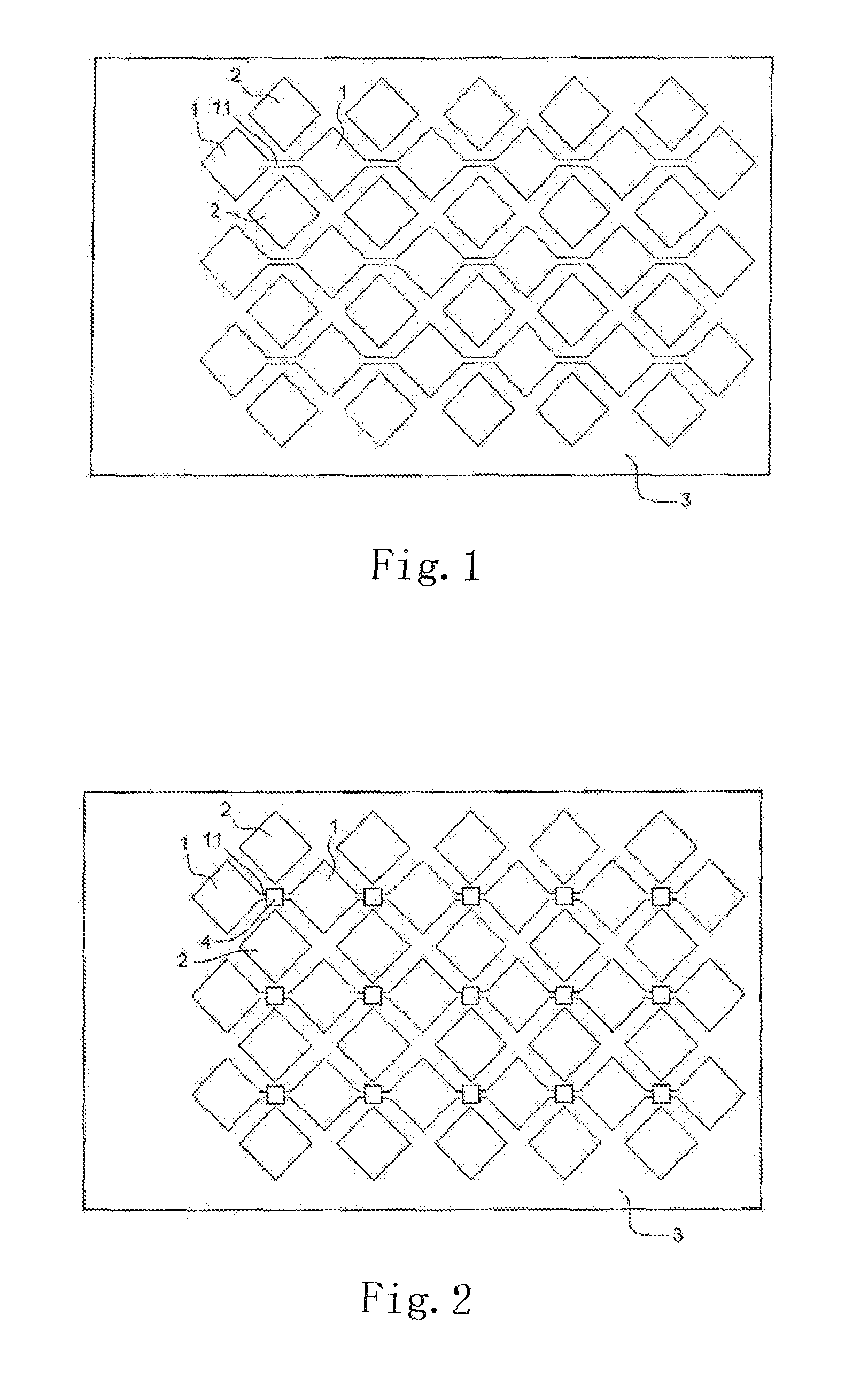
Illustratively, FIG. 3 discloses a plan view of a capacitive touch circuit pattern in accordance with the present disclosure and combining with FIG. 1 and FIG. 2, it can be seen that the present disclosure forms at least two adjacent transparent first-axis electrode blocks 1, a transparent first-axis conductive wire 11, and at least two adjacent transparent second-axis electrode blocks 2 on the surface of a substrate 3. The first-axis conductive wire 11 is formed between the two adjacent first-axis electrode blocks 1 to connect the two adjacent first-axis electrode blocks 1. The two adjacent second-axis electrode blocks 2 are disposed, respectively, at two sides of the first-axis conductive wire 11, and a second-axis conductive wire 21, which is Made of a metal material, connects the two adjacent second-axis electrode blocks 2 and stretches across the first-axis conductive wire 11. An insulation spacer 4 is formed between the first-axis conductive wire 11 and the second-axis conductive wire 21 so that the first-axis conductive wire 11 and the second-axis conductive wire 21 are electrically insulated.
A first-axis surrounding circuit 51 and a second-axis surrounding circuit 52 (as shown in FIG. 3) are respectively formed at two adjacent edges of the substrate 3, wherein the first-axis surrounding circuit 51 connects the first-axis electrode blocks 1, and the second-axis surrounding circuit 52 connects the second-axis electrode blocks 2. For the method of manufacturing a capacitive touch circuit pattern, photolithographic processing can be adopted in the present embodiment, comprising the following steps: (1) forming two adjacent first-axis electrode blocks 1, a first-axis conductive wire 11 and two adjacent second-axis electrode blocks 2 (as shown in FIG. 1) on the surface of a transparent substrate 3 through the first photolithographic processing, wherein the first-axis conductive wire 11 is disposed between the two adjacent first-axis electrode blocks 1 to connect the two adjacent first-axis electrode blocks 1, further wherein the two adjacent second-axis electrode blocks 2 are disposed, respectively, at two sides of the first-axis conductive wire 11, further wherein the first-axis electrode blocks 1, the second-axis electrode blocks 2, and the first-axis conductive wire 11 are made of a transparent conductive material and the transparent conductive material can be ITO; wherein the first-axis electrode blocks 1, the second-axis electrode blocks 2, and the first-axis conductive wire 11 can be respectively formed with multiple groups in the present embodiment, wherein the plurality of first-axis electrode blocks 1 are parallel to each other and arranged at intervals as a matrix and the plurality of second-axis electrode blocks 2 are also parallel to each other and arranged at intervals as a matrix, which makes the plurality of first-axis conductive wires 11 also arranged at intervals as a matrix; (2) based on locations of the plurality of first-axis electrode blocks 1, the second-axis electrode blocks 2, and the first-axis conductive wires 11, forming an insulation spacer 4 (as shown in FIG. 2) on the surface of the substrate 3 to cover the first-axis conductive wires 11 through a second photolithographic process, wherein the insulation spacer 4 can be made of a transparent insulation material, wherein the insulation material can be silicon oxide or other equivalent materials which have the capability of insulation. The insulation spacer 4 can also be formed with multiple groups in the present embodiment and arranged at intervals as a matrix; (3) based on the location of the insulation spacer 4, forming a second-axis conductive wire 21 which is made of a metal material, a first-axis surrounding circuit 51, and a second-axis surrounding circuit 52 (as shown in FIG. 3) on the surface of the substrate 3 through a third photolithographic process, wherein the second-axis conductive wire 21 is connected between the two adjacent second-axis electrode blocks 2 and stretches across the insulation spacer 4 so that the first-axis conductive wire 11 and the second-axis conductive wire 21 are electrically insulated, wherein the first-axis surrounding circuit 51 and the second-axis surrounding circuit 52 are disposed, respectively, at two adjacent edges of the substrate 3 so that the first-axis surrounding circuit 51 connects the first-axis electrode blocks 1 and the second-axis surrounding circuit 52 connects the second-axis electrode blocks 2.
The second-axis conductive wire 21, the first-axis surrounding circuit 51 and, the second-axis surrounding circuit 52 can be made of gold, silver, copper, aluminum or any other metal materials with good conductivity. The second-axis conductive wire 21, the first-axis surrounding circuit 51, and the second-axis surrounding circuit 52 can be formed with multiple groups in the present embodiment. The second-axis conductive wire 22 can serially connect a plurality of second-axis electrode blocks 2 by a superposition method (as shown in FIG. 4).
Thus, the first-axis electrode blocks 1 and the first-axis conductive wire 11 form a first-axis conductive element 10 and all first-axis conductive elements 10 form a capacitive sensing layer. The second-axis electrode blocks 2 and the second-axis conductive wire 21 form a second-axis conductive element 20 and all the second-axis conductive elements 20 form the other capacitive sensing layer. The capacitive sensing layers, the insulation spacers 4, and the surrounding circuits 51 and 52 form a touch circuit pattern (as shown in FIG. 3 and FIG. 4). The substrate 3 can be made of glass, plastic or any other transparent insulation material.
The capacitive touch circuit pattern structure of the present disclosure can be applied to a touch panel of a touch display screen. The touch panel comprises a substrate and a capacitive touch circuit pattern structure formed on the substrate in accordance with the present disclosure.
The touch panel can be superposed on a display panel of the touch display screen. The display panel comprises an upper substrate, a lower substrate, a pixel unit disposed between the upper and lower substrates, and a black matrix used for shading light. Preferably, the second conductive wires which are made of non-transparent conductive material in the capacitive touch circuit pattern structure are aligned with the black matrix inside the touch display screen so as to improve transmittance of the light emitted by the display panel.
When the touch circuit pattern of the present disclosure is applied to a display panel, the touch circuit pattern structure can be disposed under the upper substrate or above the lower substrate of the display panel so as to use the upper substrate or lower substrate of the display panel as a substrate of the touch panel. The second-axis conductive wires 21 and 22 can overlap with a shading layer which is used for shading light and formed by several black matrixes arranged inside the display panel. The shading layer can be omitted, using the second-axis conductive wires 21 and 22 as shading elements of the display panel, and the second-axis conductive wires 21 and 22, which are made of a metal material, can reduce the impedance between the second-axis electrode blocks 2 and the second-axis surrounding circuit 52 so as to improve sensitivity of the signal transmission between the electrode blocks and the surrounding circuits. On comparing the present disclosure with the conventional design of a whole insulation layer, the design of arranging the plurality of insulation spacers 4 at intervals as a matrix has the effect of improving the transmittance of the panel.
In accordance with the preferred embodiments it can be seen that the first-axis electrode blocks 1 and the second-axis electrode blocks 2 can be formed on the surface of the transparent substrate 3 through a single process. The touch circuit pattern can be completed through a third process, which simplifies the photolithographic processing of disposing the touch circuit pattern.
Referring to FIG. 7 which discloses a plan view of another capacitive touch circuit pattern in accordance with the preferred embodiments of the present disclosure, disposition form of this circuit pattern is similar to FIG. 3, with the difference being in the order of elements formed on the surface of the substrate. For the method of manufacturing the capacitive touch circuit pattern, photolithographic processing can be adopted in the present embodiment, comprising the following steps: (1) forming a second-axis conductive wire 21a which is made of a metal material, a first-axis surrounding circuit 51a and a second-axis surrounding circuit 52a (as shown in FIG. 5) on the surface of the substrate 3a through the first photolithographic processing, wherein the second-axis conductive wire 21a, the first-axis surrounding circuit 51a, and the second-axis surrounding circuit 52a can be, respectively, formed with multiple groups in the present embodiment; and wherein all the second-axis conductive wires 21a are disposed into arrays; (2) based on the location of the second-axis conductive wire 21a, forming an insulation spacer 4a (as shown in FIG. 6) on the surface of the substrate 3a to cover the second-axis conductive wire 21a through the second photolithographic processing, wherein the insulation spacer 4a can be formed with multiple groups in the present embodiment; (3) based on the locations of the second-axis conductive wire 21a, the insulation spacer 4a, the first-axis surrounding circuit 51a, and the second-axis surrounding circuit 52a, forming two adjacent first-axis electrode blocks 1a, a first-axis conductive wire 11a and two adjacent second-axis electrode blocks 2a (as shown in FIG. 7) on the surface of the substrate 3a through a third photolithographic process, wherein the two adjacent second-axis electrode blocks 2a are respectively connected to the two ends of the second-axis conductive wire 21a, further wherein the two first-axis electrode blocks 1a are disposed respectively at two sides of the second-axis conductive wire 21a; and wherein the first-axis conductive wire 11a stretches across the insulation spacer 4a and connects the two adjacent first-axis electrode blocks 1a so that the first-axis conductive wire 11a and the second-axis conductive wire 21a are electrically insulated.
The first-axis electrode blocks 1a, the second-axis electrode blocks 2a, and the first-axis conductive wire 11a can be respectively formed with multiple groups in the present embodiment so that the plurality of first-axis electrode blocks 1a and the second-axis electrode blocks 2a form a touch circuit pattern, and formation and implementing modes of other elements are the same as the above embodiment shown in FIG. 1.about.FIG. 3.
Referring to FIG. 10 which discloses a plan view of another capacitive touch circuit pattern in accordance with the present disclosure and combining with FIG. 8 and FIG. 9, it can be seen that the present disclosure forms two adjacent first-axis electrode blocks 1b, a first-axis conductive wire 11b and two adjacent second-axis electrode blocks 2b on a substrate 3b. The first-axis conductive wire 11b is formed between the two adjacent first-axis electrode blocks 1b to connect the two adjacent first-axis electrode blocks 1b. The two adjacent second-axis electrode blocks 2b are disposed respectively at two sides of the first-axis conductive wire 11b. The second-axis conductive wire 21b, which is made of a metal material, connects the two adjacent second-axis electrode blocks 2b and stretches across the first-axis conductive wire 11b. An insulation layer 40b is formed on the surface of the substrate 3b and filled among the first-axis electrode blocks 1b, the second-axis electrode blocks 2b, the first-axis conductive wire 11b, and the second-axis conductive wire 21b so that the first-axis conductive wire 11b and the second-axis conductive wire 21b are electrically insulated.
A first-axis surrounding circuit 51b and a second-axis surrounding circuit 52b are, respectively, formed at two adjacent edges of the substrate 3b, wherein the first-axis surrounding circuit 51b connects the first-axis electrode blocks 1b and the second-axis surrounding circuit 52b connects the second-axis electrode blocks 2b. For the method of manufacturing the capacitive touch circuit pattern, photolithographic processing can be adopted in the present embodiment, comprising the following steps: (1) forming a second-axis conductive wire 21b which is made of a metal material, a first-axis surrounding circuit 51b and a second-axis surrounding circuit 52b (as shown in FIG. 8) on the surface of the substrate 3b through a first photolithographic process, wherein the second-axis conductive wire 21b, the first-axis surrounding circuit 51b, and the second-axis surrounding circuit 52b can be, respectively, are formed with multiple groups in the present embodiment; (2) based on the location of the second-axis conductive wire 21b, forming an insulation layer 40b (as shown in FIG. 9) on the surface of the substrate 3b through a second photolithographic process, wherein there are two adjacent through-holes 41b on the surface of the insulation layer 40b, which are respectively formed above the two ends of the second-axis conductive wire 21b; wherein the insulation layer 40b can be made of a transparent insulation material and the insulation material can be silicon oxide or other equivalent materials which have the capability of insulation, and the two adjacent through-holes can be formed with multiple groups in the present embodiment; (3) based on the locations of the two adjacent through-holes 41b, forming two adjacent first-axis electrode blocks 1b, a first-axis conductive wire 11b, and two adjacent second-axis electrode blocks 2b (as shown in FIG. 10) on the insulation layer 40b on the surface of the substrate 3b through a third photolithographic process; wherein the two adjacent second-axis electrode blocks 2b are, respectively, superposed on the through-holes 41b on the surface of the insulation layer 40b and are, respectively, connected to the two ends of the second-axis conductive wire 21b, wherein the two adjacent first-axis electrode blocks 1b are disposed, respectively, at two sides of the two through-holes 41b, further wherein the first-axis conductive wire 11b is formed on the surface of the insulation layer 40b between the two through-holes 41b and connects the two adjacent first-axis electrode blocks 1b so that the first-axis conductive wire 11b and the second-axis conductive wire 21b are electrically insulated.
The first-axis electrode blocks 1b, the second-axis electrode blocks 2b, and the first-axis conductive wire 11b can be, respectively, formed with multiple groups in the present embodiment so that the plurality of the first-axis electrode blocks 1b and the second-axis electrode blocks 2b form a touch circuit pattern, and formation and implementing modes of other elements are the same as the above embodiment shown in FIG. 1.about.FIG. 3.
Referring to FIG. 13 which discloses a plan view of another capacitive touch circuit pattern in accordance with the present disclosure, its disposition form is similar to FIG. 10 and the difference is only the order of elements formed on the surface of the substrate. For the method of manufacturing the capacitive touch circuit pattern, photolithographic processing can be adopted in the present embodiment, comprising the following steps: (1) forming two adjacent first-axis electrode blocks 1c, a first-axis conductive wire 11c and two adjacent second-axis electrode blocks 2c (as shown in FIG. 11) on the surface of a transparent substrate 3c through a first photolithographic process; wherein the first-axis conductive wire 11c is disposed between the two adjacent first-axis electrode blocks 1c to connect the two adjacent first-axis electrode blocks 1c, wherein the two adjacent second-axis electrode blocks 2c are disposed, respectively, at two sides of the first-axis conductive wire 11c, further wherein the first-axis electrode blocks 1c, the second-axis electrode blocks 2c, and the first-axis conductive wire 11c can be respectively formed with multiple groups in the present embodiment; and wherein the plurality of first-axis electrode blocks 1c are parallel to each other and arranged at intervals as a matrix and the plurality of second-axis electrode blocks 2c are also parallel to each other and arranged at intervals as a matrix;
(2) based on the locations of the plurality of first-axis electrode blocks 1c, the second-axis electrode blocks 2c, and the first-axis conductive wires 11c, forming an insulation spacer 40c (as shown in FIG. 12) on the surface of the substrate 3c to cover the first-axis electrode blocks 1c, the second-axis electrode blocks 2c and the first-axis conductive wires 11c through a second photolithographic process, wherein there are two adjacent through-holes 41c on the surface of the insulation layer 40c, which are respectively formed above the second-axis electrode blocks 2c, and the two adjacent through-holes 41c can be formed with multiple groups in the present embodiment; (3) based on the locations of the two adjacent through-holes 41c, forming a second-axis conductive wire, 21c which is made of a metal material, a first-axis surrounding circuit 51c, and a second-axis surrounding circuit 52c (as shown in FIG. 13) on the surface of the substrate 3c through a third photolithographic process, wherein the second-axis conductive wire 21c is located on the surface of the insulation layer 40c between the two adjacent through-holes 41c and is superposed on the two adjacent through-holes 41c to connect the two adjacent second-axis electrode blocks 2c so that the first-axis conductive wire 11c and the second-axis conductive wire 21c are electrically insulated, further wherein the first-axis surrounding circuit 51c and the second-axis surrounding circuit 52c are disposed, respectively, at two adjacent edges of the substrate 3c so that the first-axis surrounding circuit 51c connects the first-axis electrode blocks 1c and the second-axis surrounding circuit 52c connects the second-axis electrode blocks 2c.
The second-axis conductive wire 21c, the first-axis surrounding circuit 51c and the second-axis surrounding circuit 52c can be respectively, formed with multiple groups in the present embodiment so that the plurality of first-axis electrode blocks 1c and the second-axis electrode blocks 2c form a touch circuit pattern, and formation and implementing modes of other elements are the same as the above embodiment as shown in FIG. 8.about.FIG. 10.
Although it is disclosed that the second-axis conductive wire, the first-axis surrounding circuit, and the second-axis surrounding circuit can be made of a metal material, according to the present disclosure, the second-axis conductive wire, the first-axis surrounding circuit, and/or the second-axis surrounding circuit can also be made from other non-transparent conductive materials.
Although the present disclosure refers to the embodiments and the best modes for carrying out the present disclosure, it is apparent to those skilled in the art that a variety of modifications and changes may be made without departing from the scope of the present disclosure, which is intended to be defined by the appended claims.
* * * * *
D00000
D00001
D00002
D00003
D00004
D00005
D00006
D00007
XML
uspto.report is an independent third-party trademark research tool that is not affiliated, endorsed, or sponsored by the United States Patent and Trademark Office (USPTO) or any other governmental organization. The information provided by uspto.report is based on publicly available data at the time of writing and is intended for informational purposes only.
While we strive to provide accurate and up-to-date information, we do not guarantee the accuracy, completeness, reliability, or suitability of the information displayed on this site. The use of this site is at your own risk. Any reliance you place on such information is therefore strictly at your own risk.
All official trademark data, including owner information, should be verified by visiting the official USPTO website at www.uspto.gov. This site is not intended to replace professional legal advice and should not be used as a substitute for consulting with a legal professional who is knowledgeable about trademark law.