Memory module with timing-controlled data paths in distributed data buffers
Lee , et al.
U.S. patent number 10,268,608 [Application Number 15/820,076] was granted by the patent office on 2019-04-23 for memory module with timing-controlled data paths in distributed data buffers. This patent grant is currently assigned to NETLIST, INC.. The grantee listed for this patent is Netlist, Inc.. Invention is credited to Jayesh R. Bhakta, Hyun Lee.


View All Diagrams
| United States Patent | 10,268,608 |
| Lee , et al. | April 23, 2019 |
Memory module with timing-controlled data paths in distributed data buffers
Abstract
A memory module is operable in a memory system with a memory controller. The memory module comprises memory devices, a module control circuit, and a plurality of buffer circuits coupled between respective sets of data/strobe signal lines in a data bus and respective sets of the memory devices. Each respective buffer circuit includes a data path corresponding to each data signal line in the corresponding set of data/strobe signal lines, and a command processing circuit configured to decode module control signals from the module control circuit and to control the data path in accordance with the module control signals. The data path corresponding to the each data signal line includes at least one tristate buffer controlled by the command processing circuit and a delay circuit configured to delay a signal through the data path by an amount determined by the command processing circuit in response to at least one of the module control signals.
| Inventors: | Lee; Hyun (Ladera Ranch, CA), Bhakta; Jayesh R. (Cerritos, CA) | ||||||||||
|---|---|---|---|---|---|---|---|---|---|---|---|
| Applicant: |
|
||||||||||
| Assignee: | NETLIST, INC. (Irvine,
CA) |
||||||||||
| Family ID: | 51865689 | ||||||||||
| Appl. No.: | 15/820,076 | ||||||||||
| Filed: | November 21, 2017 |
Prior Publication Data
| Document Identifier | Publication Date | |
|---|---|---|
| US 20180095908 A1 | Apr 5, 2018 | |
Related U.S. Patent Documents
| Application Number | Filing Date | Patent Number | Issue Date | ||
|---|---|---|---|---|---|
| 15426064 | Nov 21, 2017 | 9824035 | |||
| 14846993 | Feb 7, 2017 | 9563587 | |||
| 13952599 | Sep 8, 2015 | 9128632 | |||
| 61676883 | Jul 27, 2012 | ||||
| Current U.S. Class: | 1/1 |
| Current CPC Class: | G11C 7/1066 (20130101); G06F 3/0647 (20130101); G06F 3/0613 (20130101); G06F 1/10 (20130101); G06F 3/0683 (20130101); G06F 3/0656 (20130101); G06F 3/0659 (20130101); G11C 5/04 (20130101); G11C 16/00 (20130101); G11C 8/18 (20130101); G06F 13/1673 (20130101); H05K 999/99 (20130101); G06F 13/1642 (20130101); G06F 13/4027 (20130101); G11C 29/023 (20130101); G06F 13/28 (20130101); G11C 7/1006 (20130101); G11C 29/028 (20130101); G11C 7/1093 (20130101); G11C 8/12 (20130101); G11C 7/109 (20130101); G11C 2029/0407 (20130101); G11C 7/20 (20130101) |
| Current International Class: | G06F 3/00 (20060101); G06F 13/40 (20060101); G06F 13/28 (20060101); G06F 1/10 (20060101); G11C 29/02 (20060101); G11C 5/04 (20060101); G11C 8/18 (20060101); G06F 12/00 (20060101); G06F 13/00 (20060101); G06F 13/16 (20060101); G06F 3/06 (20060101); G11C 16/00 (20060101); G11C 7/10 (20060101); G11C 29/04 (20060101); G11C 8/12 (20060101); G11C 7/20 (20060101) |
References Cited [Referenced By]
U.S. Patent Documents
| 4218740 | August 1980 | Bennett et al. |
| 4249253 | February 1981 | Gentili et al. |
| 4368515 | January 1983 | Nielsen |
| 4392212 | July 1983 | Miyasaka et al. |
| 4571676 | February 1986 | Mantellina et al. |
| 4592011 | May 1986 | Mantellina et al. |
| 4633429 | December 1986 | Lewandowski et al. |
| 4670748 | June 1987 | Williams |
| 4706214 | November 1987 | Kassai |
| 4739473 | April 1988 | Ng |
| 4866603 | September 1989 | Chiba |
| 4958322 | September 1990 | Kosugi et al. |
| 4961172 | October 1990 | Shubat et al. |
| 4961204 | October 1990 | Tanaka et al. |
| 4980850 | December 1990 | Morgan |
| 5060188 | October 1991 | Zulian et al. |
| 5247643 | September 1993 | Shottan |
| 5272664 | December 1993 | Alexander et al. |
| 5313624 | May 1994 | Harriman |
| 5345412 | September 1994 | Shiratsuchi |
| 5357478 | October 1994 | Kikuda et al. |
| 5388072 | February 1995 | Matick et al. |
| 5388240 | February 1995 | Olderdissen et al. |
| 5392252 | February 1995 | Rimpo et al. |
| 5426753 | June 1995 | Moon |
| 5463590 | October 1995 | Watanabe |
| 5483497 | January 1996 | Mochizuki et al. |
| 5485589 | January 1996 | Kocis et al. |
| 5495435 | February 1996 | Sugahara |
| 5513135 | April 1996 | Dell et al. |
| 5532954 | July 1996 | Bechtolsheim et al. |
| 5537584 | July 1996 | Miyai et al. |
| 5541448 | July 1996 | Carpenter |
| 5572691 | November 1996 | Koudmani |
| 5581498 | December 1996 | Ludwig et al. |
| 5590071 | December 1996 | Kolor et al. |
| 5602999 | February 1997 | Hyatt |
| 5617559 | April 1997 | Le et al. |
| 5630096 | May 1997 | Zuravleff |
| 5638534 | June 1997 | Mote, Jr. |
| 5649159 | July 1997 | Le et al. |
| 5655113 | August 1997 | Leung |
| 5655153 | August 1997 | Sandorfi |
| 5699542 | December 1997 | Mehta et al. |
| 5702984 | December 1997 | Bertin et al. |
| 5703826 | December 1997 | Hush et al. |
| 5717851 | February 1998 | Yishay et al. |
| 5724604 | March 1998 | Moyer |
| 5745914 | April 1998 | Connolly et al. |
| 5729716 | May 1998 | Lee et al. |
| 5764590 | June 1998 | Iwamoto et al. |
| 5784705 | July 1998 | Leung |
| 5802395 | September 1998 | Connolly et al. |
| 5802541 | September 1998 | Reed |
| 5805520 | September 1998 | Anglada et al. |
| 5822251 | October 1998 | Bruce et al. |
| 5905401 | May 1999 | Sher |
| RE36229 | June 1999 | Cady |
| 5909388 | June 1999 | Mueller |
| 5926827 | July 1999 | Dell et al. |
| 5926839 | July 1999 | Katayama |
| 5953215 | September 1999 | Karabatsos |
| 5953280 | September 1999 | Watsui |
| 5958025 | September 1999 | Sonobe |
| 5959930 | September 1999 | Sakurai |
| 5963464 | October 1999 | Dell et al. |
| 5966736 | October 1999 | Gittinger et al. |
| 5973392 | October 1999 | Senba et al. |
| 5974493 | October 1999 | Okumura et al. |
| 6011710 | January 2000 | Wieggers |
| 6018787 | January 2000 | Ip |
| 6044032 | March 2000 | Li |
| 6061754 | May 2000 | Cepulis |
| 6070217 | May 2000 | Connolly et al. |
| 6070227 | May 2000 | Rokicki |
| 6097652 | August 2000 | Roh |
| 6108745 | August 2000 | Gupta et al. |
| 6115278 | September 2000 | Deneroff et al. |
| 6134638 | October 2000 | Olarig et al. |
| 6141245 | October 2000 | Bertin |
| 6151271 | November 2000 | Lee |
| 6154418 | November 2000 | Li |
| 6154419 | November 2000 | Shakkarwar |
| 6173357 | January 2001 | Ju |
| 6185654 | February 2001 | Van Doren |
| 6188641 | February 2001 | Uchida |
| 6205516 | March 2001 | Usami |
| 6209074 | March 2001 | Dell et al. |
| 6223650 | May 2001 | Johnson |
| 6226709 | May 2001 | Goodwin et al. |
| 6226736 | May 2001 | Niot |
| 6233650 | May 2001 | Johnson et al. |
| 6247088 | June 2001 | Seo et al. |
| 6260127 | July 2001 | Olarig et al. |
| 6262938 | July 2001 | Lee |
| 6317352 | November 2001 | Halbert et al. |
| 6349051 | February 2002 | Klein |
| 6381140 | April 2002 | Liao |
| 6400637 | June 2002 | Akamatsu et al. |
| 6408356 | June 2002 | Dell |
| 6414868 | July 2002 | Wong et al. |
| 6415374 | July 2002 | Faue et al. |
| 6438062 | August 2002 | Curtis |
| 6446158 | September 2002 | Karabatsos |
| 6446184 | September 2002 | Dell et al. |
| 6453381 | September 2002 | Yuan et al. |
| 6470417 | October 2002 | Kolor et al. |
| 6480439 | November 2002 | Tokutome et al. |
| 6487102 | November 2002 | Halbert et al. |
| 6502161 | December 2002 | Perego et al. |
| 6518794 | February 2003 | Coteus et al. |
| 6526473 | February 2003 | Kim |
| 6530007 | March 2003 | Olarig et al. |
| 6530033 | March 2003 | Raynham et al. |
| 6546476 | April 2003 | Gillingham |
| 6553449 | April 2003 | Dodd et al. |
| 6553450 | April 2003 | Dodd et al. |
| 6618320 | September 2003 | Hasegawa et al. |
| 6618791 | September 2003 | Dodd et al. |
| 6621496 | September 2003 | Ryan |
| 6625081 | September 2003 | Roohparvar et al. |
| 6625687 | September 2003 | Halbert et al. |
| 6636446 | October 2003 | Lee |
| 6636935 | October 2003 | Ware et al. |
| 6646949 | November 2003 | Ellis et al. |
| 6658509 | December 2003 | Bonella et al. |
| 6674684 | January 2004 | Shen |
| 6681301 | January 2004 | Mehta et al. |
| 6683372 | January 2004 | Wong et al. |
| 6697888 | February 2004 | Halbert et al. |
| 6704910 | March 2004 | Hong |
| 6705877 | March 2004 | Li et al. |
| 6717855 | April 2004 | Underwood |
| 6717885 | April 2004 | Lai |
| 6721843 | April 2004 | Estakhri |
| 6721860 | April 2004 | Klein |
| 6738880 | May 2004 | Lai et al. |
| 6742098 | May 2004 | Halbert et al. |
| 6747887 | June 2004 | Halbert et al. |
| 6754746 | June 2004 | Leung et al. |
| 6754797 | June 2004 | Wu et al. |
| 6785189 | August 2004 | Jacobs et al. |
| 6788592 | September 2004 | Nakata et al. |
| 6799252 | September 2004 | Bauman |
| 6807125 | October 2004 | Coteus et al. |
| 6807650 | October 2004 | Lamb et al. |
| 6813196 | November 2004 | Park et al. |
| 6832303 | December 2004 | Tanaka |
| 6834014 | December 2004 | Yoo et al. |
| 6854042 | February 2005 | Karabatsos |
| 6880094 | April 2005 | La Berge |
| 6889304 | May 2005 | Perego et al. |
| 6912615 | June 2005 | Nicolai |
| 6912628 | June 2005 | Wicki et al. |
| 6925028 | August 2005 | Hosokawa et al. |
| 6944694 | September 2005 | Pax |
| 6948084 | September 2005 | Manapat et al. |
| 6950366 | September 2005 | Lapidus et al. |
| 6954281 | October 2005 | Fukuda et al. |
| 6961281 | November 2005 | Wong et al. |
| 6981089 | December 2005 | Dodd et al. |
| 6982892 | January 2006 | Lee et al. |
| 6982893 | January 2006 | Jakobs |
| 6990043 | January 2006 | Kuroda et al. |
| 6996686 | February 2006 | Doblar et al. |
| 7007130 | February 2006 | Holman |
| 7007175 | February 2006 | Chang et al. |
| 7024518 | April 2006 | Halbert et al. |
| 7046538 | May 2006 | Kinsley et al. |
| 7047361 | May 2006 | Chong et al. |
| 7054179 | May 2006 | Cogdill et al. |
| 7065626 | June 2006 | Schumacher et al. |
| 7072231 | July 2006 | Pax |
| 7073041 | July 2006 | Dwyer et al. |
| 7078793 | July 2006 | Ruckerbauer et al. |
| 7093066 | August 2006 | Klein |
| 7120727 | October 2006 | Lee et al. |
| 7124260 | October 2006 | La Berge et al. |
| 7127584 | October 2006 | Thompson et al. |
| 7130308 | October 2006 | Haddock et al. |
| 7130952 | October 2006 | Nanki et al. |
| 7133960 | November 2006 | Thompson et al. |
| 7133972 | November 2006 | Jeddeloh |
| 7142461 | November 2006 | Janzen |
| 7149841 | December 2006 | La Berge |
| 7167967 | January 2007 | Bungo et al. |
| 7181591 | February 2007 | Tsai |
| 7191302 | March 2007 | Usami |
| 7200021 | April 2007 | Radhuram |
| 7225303 | May 2007 | Choi |
| 7227910 | June 2007 | Lipka |
| 7254036 | August 2007 | Pauley et al. |
| 7266639 | September 2007 | Radhuram |
| 7272709 | September 2007 | Zitlaw et al. |
| 7281079 | October 2007 | Bains et al. |
| 7286436 | October 2007 | Bhakta et al. |
| 7289386 | October 2007 | Bhakta et al. |
| 7334150 | February 2008 | Ruckerbauer et al. |
| 7346750 | March 2008 | Ishikawa |
| 7356639 | April 2008 | Perego et al. |
| 7370238 | May 2008 | Billick et al. |
| 7379361 | May 2008 | Co et al. |
| 7437591 | October 2008 | Wong |
| 7461182 | December 2008 | Fukushima et al. |
| 7464225 | December 2008 | Tsern |
| 7471538 | December 2008 | Hofstra |
| 7532537 | May 2009 | Solomon et al. |
| 7619912 | November 2009 | Bhakta et al. |
| 7636274 | December 2009 | Solomon et al. |
| 7730254 | June 2010 | Risse |
| 7864627 | January 2011 | Bhakta et al. |
| 7865674 | January 2011 | Gower et al. |
| 7881150 | February 2011 | Solomon et al. |
| 7884619 | February 2011 | Chong |
| 7916574 | March 2011 | Solomon et al. |
| 7990746 | August 2011 | Rajan |
| 8001434 | August 2011 | Lee et al. |
| 8081536 | December 2011 | Solomon et al. |
| 8089795 | January 2012 | Rajan |
| 8130560 | March 2012 | Rajan et al. |
| 8189328 | May 2012 | Kanapathippillai |
| 8214616 | July 2012 | Ware |
| 8233303 | July 2012 | Best |
| 8244971 | August 2012 | Rajan |
| 8250295 | August 2012 | Amidi et al. |
| 8335894 | December 2012 | Rajan |
| 8417870 | April 2013 | Lee et al. |
| 8516185 | August 2013 | Lee et al. |
| 8516188 | August 2013 | Solomon et al. |
| 8565033 | October 2013 | Manochararajah et al. |
| 8689064 | April 2014 | Lee et al. |
| 8756364 | June 2014 | Bhakta et al. |
| 8782350 | July 2014 | Lee et al. |
| 8856464 | October 2014 | Karamcheti |
| 8949519 | February 2015 | Rajan |
| 2001/0008006 | July 2001 | Klein |
| 2002/0038405 | March 2002 | Leddige |
| 2002/0039323 | April 2002 | Tokutome |
| 2002/0048195 | April 2002 | Klein |
| 2002/0112119 | August 2002 | Halbert et al. |
| 2003/0070052 | April 2003 | Lai |
| 2004/0098528 | May 2004 | Janzen |
| 2004/0105292 | June 2004 | Matsui |
| 2005/0010737 | January 2005 | Ware et al. |
| 2005/0257109 | November 2005 | Averbui |
| 2005/0281096 | December 2005 | Bhakta et al. |
| 2006/0077731 | April 2006 | Ware |
| 2006/0117152 | June 2006 | Amidi et al. |
| 2006/0179206 | August 2006 | Brittain et al. |
| 2006/0233012 | October 2006 | Sekiguchi et al. |
| 2006/0259711 | November 2006 | Oh |
| 2006/0262586 | November 2006 | Solomon et al. |
| 2006/0267172 | November 2006 | Nguyen et al. |
| 2006/0277355 | December 2006 | Ellsberry et al. |
| 2007/0058409 | March 2007 | Ruckerbauer |
| 2007/0064462 | March 2007 | Matsui |
| 2007/0070669 | March 2007 | Tsern |
| 2007/0217559 | September 2007 | Stott |
| 2007/0293094 | December 2007 | Aekins |
| 2008/0025137 | January 2008 | Rajan et al. |
| 2008/0037412 | February 2008 | Geile |
| 2008/0046631 | February 2008 | Takaku et al. |
| 2008/0104352 | May 2008 | Talbot |
| 2008/0162790 | July 2008 | Im |
| 2009/0103387 | April 2009 | Shau |
| 2009/0198924 | August 2009 | Shaeffer et al. |
| 2009/0248969 | October 2009 | Wu et al. |
| 2009/0296503 | December 2009 | Chu |
| 2010/0070690 | March 2010 | Amer et al. |
| 2010/0091540 | April 2010 | Bhakta et al. |
| 2010/0125681 | May 2010 | Patel |
| 2010/0228891 | September 2010 | Talbot |
| 2010/0271092 | October 2010 | Zerbe |
| 2011/0016250 | January 2011 | Lee et al. |
| 2011/0016269 | January 2011 | Lee et al. |
| 2011/0085408 | April 2011 | Solomon |
| 2011/0090749 | April 2011 | Bhakta et al. |
| 2011/0125966 | May 2011 | Amidi et al. |
| 2012/0256639 | October 2012 | Pausini |
| 2014/0029370 | January 2014 | Koshizuka |
| 1816570 | Aug 2007 | EP | |||
| 09237492 | Sep 1997 | JP | |||
| I0-092169 | Oct 1998 | JP | |||
| 2000285674 | Oct 2000 | JP | |||
| 2000311485 | Oct 2000 | JP | |||
| 2002184176 | Jun 2002 | JP | |||
| 2003007963 | Jan 2003 | JP | |||
| 2008046989 | Feb 2008 | JP | |||
Other References
|
US 6,832,284 B1, 12/2004, Perego et al. (withdrawn) cited by applicant . Non-Final Office Action, U.S. Appl. No. 13/412,243, dated Jan. 2, 2014, 20 pages. cited by applicant . Non-final office action, U.S. Appl. No. 13/288,850, dated Oct. 11, 2013, 24 pages. cited by applicant . Non-final office action, U.S. Appl. No. 13/411,344, dated Dec. 31, 2013, 28 pages. cited by applicant . Non-final office action, U.S. Appl. No. 13/473,413, dated Nov. 17, 2011, 46 pages. cited by applicant . Response to non-final office action dated Oct. 14, 2013 for U.S. Appl. No. 13/288,850, filed Jan. 13, 2014, 15 pages. cited by applicant . Response to non-final office action dated Dec. 31, 2013 for U.S. Appl. No. 13/411,344, filed Mar. 31, 2014, 12 pages. cited by applicant . Patent Owner's Response to Office Action dated Nov. 13, 2012 for Reexamination Control Nos. 95/000,578; 95/000,579, and 95/001,339, filed Jan. 14, 2013, 96 pages. cited by applicant . Patent Owner's Response to Office Action dated Dec. 19, 2012 for Reexamination Control No. 95/001,758, filed Mar. 19, 2013, 61 pages. cited by applicant . Patent Owner's Response to Office Action dated Sep. 26, 2013 for Reexamination Control No. 95/001,758, filed Nov. 26, 2013, 85 pages. cited by applicant . Third Party Requester's Comments after Non-Final Action dated Sep. 26, 2013 for Reexamination Control No. 95/001,758, filed Dec. 26, 2013,. cited by applicant . Patent Owner's Appeal Brief for Reexamination Control Nos. 95/000,546 and 95/000,577, filed Oct. 2, 2013, 46 pages. cited by applicant . Patent Trial and Appeal Board Decision on Appeal for Reexamination Control No. 95/001/337, mailed Jan. 16, 2014, 30 pages. cited by applicant . Patent Trial and Appeal Board Decision on Appeal for Reexamination Control No. 95/001/381, mailed Jan. 16, 2014, 24 pages. cited by applicant . Action Closing Prosecution mailed Mar. 27, 2014 for Reexamination Control No. 95/001,758, filed Sep. 14, 2011, 40 pages. cited by applicant . Action Closing Prosecution mailed Mar. 27, 2014 for Reexamination Control No. 95/001,339, filed Jun. 8, 2010, 106 pages. cited by applicant . Notice of Allowance, U.S. Appl. No. 12/504,131, dated Feb. 12, 2013, 52 pgs. cited by applicant . Response to Non-Final Office Action dated Jan. 2, 2014, filed Apr. 2, 2004, for U.S. Appl. No. 13/287,042, filed Nov. 1, 2011, 12 pages. cited by applicant . Non-Final Action Closing Prosecution mailed Sep. 1, 2010, for Control No. 95/001,339, filed Apr. 10, 2010, 17 pages. cited by applicant . Non-Final Action Closing Prosecution mailed Jun. 21, 2011, for Control No. 95/001,381, filed Jun. 9, 2010, 34 pages. cited by applicant . Non-Final Action Closing Prosecution mailed Mar. 12, 2012, for Control No. 95/001,337, filed Apr. 19, 2010, 33 pages. cited by applicant . Non-Final Action mailed Aug. 27, 2010, for Control No. 95/000,546, filed May 11, 2010, 16 pages. cited by applicant . Non-Final Action mailed Sep. 8, 2010, for Control No. 95/001,381, filed Jun. 9, 2010, 17 pages. cited by applicant . Non-Final Action mailed Apr. 4, 2011, for Control No. 95/001,339, filed Apr. 20, 2010, 61 pages. (merged with 95/000,578 and 95/000,579). cited by applicant . Non-Final Action mailed Jun. 15, 2011, for Control No. 95/001,381, filed Jun. 9, 2010, 33 pages. cited by applicant . Non-Final Action mailed Sep. 27, 2011, for Control No. 95/001,337, filed Apr. 19, 2010, 19 pages. cited by applicant . Non-Final Action mailed Oct. 4, 2011, for Control No. 95/001,339, filed Apr. 20, 2010, 77 pages. (merged with 95/000,578 and 95/000,579). cited by applicant . Non-Final Action mailed Oct. 14, 2011, for Control No. 95/001,339, filed Apr. 30, 2010, 99 pages. (merged with 95/000,578 and 95/000,579). cited by applicant . Non-Final Office Action dated Nov. 16, 2011, for U.S. Appl. No. 95/001,758 filed Sep. 14, 2011, 25 pages. cited by applicant . Reexam Appl. No. 95/000,546 for U.S. Pat. No. 7,289,386, filed May 11, 2010, Netlist, Inc., Entire File History. cited by applicant . Reexam Appl. No. 95/000,577 for U.S. Pat. No. 7,289,386, filed Oct. 20, 2010, Netlist, Inc., Entire File History. cited by applicant . Reexam Appl. No. 95/000,578 for U.S. Pat. No. 7,619,912, filed Oct. 20, 2010, Netlist, Inc., Entire File History. cited by applicant . Reexam Appl. No. 95/000,579 for U.S. Pat. No. 7,619,912, filed Oct. 21, 2010, Netlist, Inc., Entire File History. cited by applicant . Reexam App. No. 95/001,337 for U.S. Pat. No. 7,636,274, filed Jun. 4, 2010, Netlist, Inc., Entire File History. cited by applicant . Reexam Appl. No. 95/001,381 for U.S. Pat. No. 7,532,537, filed Jun. 9, 2010, Netlist, Inc., Entire File History. cited by applicant . Reexam Appl. No. 95/001,338; for U.S. Pat. No. 7,532,537, filed Apr. 19, 2010, Netlist, Inc., Entire File History. cited by applicant . Reexam Appl. No. 95/001,758 for U.S. Pat. No. 7,864,627, filed Sep. 15, 2010, Netlist, Inc., Entire File History. cited by applicant . Reexam Appl. No. 95/001,339 for U.S. Pat. No. 7,619,912, filed Jun. 8, 2010 Netlist, Inc., Entire File History. cited by applicant . Reexam Appl. No. 95/002,399 for U.S. Pat. No. 8,250,295, filed Sep. 15, 2010, Netlist, Inc., Entire File History. cited by applicant . U.S. Appl. No. 11/075,395, filed Mar. 7, 2005 Netlist Inc., Entire Prosecution History. cited by applicant . U.S. Appl. No. 11/173,175, filed Jul. 1, 2005 Netlist, Inc., Entire Prosecution History. cited by applicant . U.S. Appl. No. 11/862,931, filed Sep. 27, 2007 Netlist, Inc., Entire Prosecution History. cited by applicant . U.S. Appl. No. 12/577,682, filed Oct. 12, 2009, Netlist, Inc., Entire Prosecution History. cited by applicant . U.S. Appl. No. 12/954,492, filed Nov. 24, 2010, Netlist, Inc., Entire Prosecution History. cited by applicant . U.S. Appl. No. 12/912,623, filed Oct. 26, 2010, Netlist, Inc., Entire Prosecution History. cited by applicant . U.S. Appl. No. 11/335,875, filed Jan. 19, 2006, Netlist, Inc., Entire Prosecution History. cited by applicant . U.S. Appl. No. 12/408,652, filed Mar. 20, 2009, Netlist, Inc., Entire Prosecution History. cited by applicant . U.S. Appl. No. 12/629,827, filed Dec. 2, 2009, Netlist Inc., Entire Prosecution History. cited by applicant . U.S. Appl. No. 12/955,711, filed Nov. 29, 2010, Netlist, Inc., Entire Prosecution History. cited by applicant . U.S. Appl. No. 12/981,380, filed Dec. 29, 2010, Netlist Inc., Entire Prosecution History. cited by applicant . U.S. Appl. No. 13/154,172, filed Jun. 6, 2011, Netlist, Inc., Entire Prosecution History. cited by applicant . U.S. Appl. No. 13/287,042, filed Nov. 1, 2011, Netlist, Inc., Entire Prosecution History. cited by applicant . U.S. Appl. No. 13/473,413, filed May 16, 2012, Netlist, Inc., Entire Prosecution History. cited by applicant . U.S. Appl. No. 13/032,470, filed Feb. 22, 2011, Netlist Inc., Entire Prosecution History. cited by applicant . U.S. Appl. No. 13/287,081, filed Nov. 1, 2011, Netlist, Inc., Entire Prosecution History. cited by applicant . U.S. Appl. No. 13/971,231, filed Aug. 20, 2013, Netlist, Inc., Entire Prosecution History. cited by applicant . U.S. Appl. No. 12/422,853, filed Apr. 13, 2009, Netlist, Inc., Entire Prosecution History. cited by applicant . U.S. Appl. No. 13/412,243, filed Mar. 5, 2012, Netlist, Inc., Entire Prosecution History. cited by applicant . U.S. Appl. No. 12/422,925, filed Apr. 13, 2009, Netlist, Inc., Entire Prosecution History. cited by applicant . U.S. Appl. No. 13/183,253, filed Jul. 14, 2011, Netlist, Inc., Entire Prosecution History. cited by applicant . U.S. Appl. No. 13/745,790, filed Jan. 19, 2013, Netlist, Inc., Entire Prosecution History. cited by applicant . U.S. Appl. No. 14/229,844, filed Mar. 29, 2014, Netlist, Inc., Entire Prosecution History. cited by applicant . U.S. Appl. No. 12/504,131, filed Jul. 16, 2009, Netlist, Inc., Entire Prosecution History. cited by applicant . U.S. Appl. No. 12/761,179, filed Apr. 15, 2010, Netlist, Inc., Entire Prosecution History. cited by applicant . U.S. Appl. No. 13/288,850, filed Nov. 3, 2011, Netlist, Inc., Entire Prosecution History. cited by applicant . U.S. Appl. No. 13/411,344, filed Mar. 2, 2012, Netlist, Inc., Entire Prosecution History. cited by applicant . U.S. Appl. No. 13/952,599, filed Jul. 27, 2013, Netlist, Inc., Entire Prosecution History. cited by applicant . U.S. Appl. No. 13/411,344, filed Mar. 2, 201, Lee, Entire Prosecution. cited by applicant . U.S. Appl. No. 13/970,606, filed Aug. 20, 20, Netlist, Entire Prosecution. cited by applicant . U.S. Appl. No. 13/971,231, filed Aug. 20, 20, Netlist, Entire Prosecution. cited by applicant . U.S. Appl. No. 14/229,844, Mar. 29, 20, Netlist, Entire Prosecution. cited by applicant . U.S. Appl. No. 14/324,990, filed Jul. 7, 201, Netlist, Entire Prosecution. cited by applicant . U.S. Appl. No. 14/337,168, filed Jul. 21, 20, Netlist, Entire Prosecution. cited by applicant . International Search Report and Written Opinion, PCT/US2010/040826, Sep. 27. cited by applicant . Written Opinion of the International Preliminary Examining Authority, PCT/US2010/040826, dated Oct. 24, 2011. cited by applicant . International Preliminary Report on Patentability, PCT/US2010/040826, dated Nov. 28. cited by applicant . International Search Report and Written Opinion, PCT/US2011/059209, dated Jan. 30, 2013. cited by applicant . Notice of Allowance dated Feb. 12, 2013, for U.S. Appl. No. 12/504,131, filed Jul. 16, 2009, 52 pages. cited by applicant . Non-Final Office Action dated Sep. 13, 2012, for U.S. Appl. No. 12/761,179, filed Apr. 15, 2010, 20 pages. cited by applicant . Response to Non-Final Office Action dated Sep. 13, 2012, for U.S. Appl. No. 12/761,179, filed Mar. 13, 2013, 16 pages. cited by applicant . Notice of Allowance dated Jul. 11, 2013, for U.S. Appl. No. 12/761,179 filed Apr. 15, 2010, 37 pages. cited by applicant . Inter Partes Review Case No. IPR2014-01029, Petition for Inter Partes Review of U.S. Pat. No. 8,516,185, filed on Jun. 24, 2014. cited by applicant . Inter Partes Review Case No. IPR2014-01029, Exhibit 1008 to Petition for Inter Partes Review, "Declaration of Charles J. Neuhauser, Ph.D. under 37 C.F.R. .sctn. 1.68," filed on Jun. cited by applicant . Inter Partes Review Case No. IPR2014-01029, Patent Owner's Preliminary Response pursuant to 37 C.F.R. .sctn. 42.107, filed on Oct. 17, 2014. cited by applicant . Inter Partes Review Case No. IPR2014-01029, Decision Denying Institution of Inter Partes Review 37 C.F.R. .sctn. 42.108, issued Dec. 16, 2014. cited by applicant . Inter Partes Review Case No. IPR2014-01369, Corrected Petition for Inter Partes Review of Claims 1-19 of U.S. Pat. No. 8,516,185, filed on Sep. 22, 2014. cited by applicant . Inter Partes Review Case No. IPR2014-01369, Exhibit 1008 to Corrected Petition for Inter Partes Review, "Declaration of Dr. Nader Bagherzadeh under 37 C.F.R. .sctn. 1.68," filed on Sep. 22, 2014. cited by applicant . Inter Partes Review Case No. IPR2014-01369, Exhibit 1013 to Corrected Petition for Inter Partes Review, "Webster's II New College Dictionary," filed on Sep. 22, 2014. cited by applicant . Inter Partes Review Case No. IPR2014-01369, Exhibit 1014 to Corrected Petition for Inter Partes Review, "Standard Dictionary of Electrical and Electronics Terms," IEEE 1988, filed on Sep. 22, 2014. cited by applicant . Inter Partes Review of U.S. Pat. No. 7,881,150, IPR Case No. IPR2014-00882, Corrected Petition for Inter Partes Review of U.S. Pat. No. 7,881,150, filed on Jul. 8. cited by applicant . Inter Partes Review of U.S. Pat. No. 7,881,150, IPR Case No. IPR2014-00882, Exhibit 1007 to Petition for Inter Partes Review, "Declaration of Dr. Srinivasan Jagannathan," filed on Jun. 22, 2014. cited by applicant . Inter Partes Review of U.S. Pat. No. 7,881,150, IPR Case No. IPR2014-00882, Patent Owner's Preliminary Response Pursuant to 37 C.F.R. .sctn. 42.107, filed Oct. 7, 2014. cited by applicant . Inter Partes Review of U.S. Pat. No. 7,881,150, IPR Case No. IPR2014-00882, Decision--Institution of Inter Partes Review 37 C.F.R. .sctn. 42.108, issued Dec. 16. cited by applicant . Inter Partes Review of U.S. Pat. No. 8,081,536, IPR Case No. IPR2014-00883, Corrected Petition for Inter Partes Review of U.S. Pat. No. 8,081,536, filed on Jul. 8. cited by applicant . Inter Partes Review of U.S. Pat. No. 8,081,536, IPR Case No. IPR2014-00883, Exhibit 1011 to Petition for Inter Partes Review, "Declaration of Dr. Srinivasan Jagannathan," filed on Jun. 21, 2014. cited by applicant . Inter Partes Review of U.S. Pat. No. 8,081,536, IPR Case No. IPR2014-00883, Patent Owner's Preliminary Response Pursuant to 37 C.F.R. .sctn. 42.107, filed Oct. 7, 2014. cited by applicant . Inter Partes Review of U.S. Pat. No. 8,081,536, IPR Case No. IPR2014-00883, Decision--Institution of Inter Partes Review 37 C.F.R. .sctn. 42.108, issued Dec. 16. cited by applicant . Inter Partes Review of U.S. Pat. No. 7,881,150, IPR Case No. IPR2014-01011, Corrected Petition for Inter Partes Review ofU.S. Pat. No. 7,881,150, filed on Jul. 8. cited by applicant . Inter Partes Review of U.S. Pat. No. 7,881,150, IPR Case No. IPR2014-01011, Exhibit 1007 to Petition for Inter PartesReview, "Declaration of Dr. Srinivasan Jagannathan." filed on Jun. 22, 2014. cited by applicant . Inter Partes Review of U.S. Pat. No. 7,881,150, IPR Case No. IPR2014-01011, Patent Owner's Preliminary Response Pursuant to 37 C.F.R. .sctn. 42.107, filed Oct. 7, 2014. cited by applicant . Inter Partes Review of U.S. Pat. No. 7,881,150, IPR Case No. IPR2014-01011, Decision--Institution of Inter Partes Review 37 C.F.R. .sctn. 42.108, issued Dec. 16. cited by applicant . Inter Partes Review of U.S. Pat. No. 7,881,150, IPR Case No. IPR2014-01011, Exhibit 3001 to Decision--Institution of Inter Partes Review, Excerpts from IEEE Dictionary, issued Dec. 16, 2014. cited by applicant . Inter Partes Review of U.S. Pat. No. 7,881,150, IPR Case No. IPR2014-01011, Exhibit 3002 to Decision--Institution of Inter Partes Review, Excerpts from IEEE Dictionary, issued Dec. 16,2014. cited by applicant . Inter Partes Review of U.S. Pat. No. 7,881,150, IPR Case No. IPR2014-01011, Exhibit 3003 to Decision--Institution of Inter Partes Review, Excerpts from Oxford English Dictionary, issued Dec. 16, 2014. cited by applicant . Inter Partes Review of U.S. Pat. No. 7,881,150, IPR Case No. IPR2014-01011, Exhibit 3004 to Decision--Institution of Inter Partes Review, Excerpts from Oxford English Dictionary, issued Dec. 16, 2014. cited by applicant . McCluskey, Edward J., Logic Design Principles with Emphasis on Testable Semicustom Circuits, Prentice Hall, 1986, pp. 104-107 and 119-120. cited by applicant . U.S. District Court Northern District of California, Case No. 4:13-CV-05889-YGR, Netlist, Inc. v. Smart Storage Systems, Inc., and Diablo Technologies, Inc., Smart Storage Systems, Inc.'s Invalidity Contentions, dated Jun. 6, 2014. cited by applicant . U.S. District Court Northern District of California, Case No. 4:13-CV-05889-YGR, Netlist, Inc. v. Smart Storage Systems, Inc., and Diablo Technologies, Inc., Exhibits E.1-E.7 to "Smart Storage Systems, Inc.'s Invalidity Contentions," dated Jun. 6, 2014. cited by applicant . U.S. District Court Northern District of California, Case No. 4:13-CV-05889-YGR, Netlist, Inc. v. Smart Storage Systems, Inc., and Diablo Technologies, Inc., Exhibits F.1-F.5 to "Smart Storage Systems, Inc.'s Invalidity Contentions," dated Jun. 6, 2014. cited by applicant . U.S. District Court Northern District of California, Case No. 4:13-CV-05889-YGR, Netlist, Inc. v. Smart Storage Systems, Inc., and Diablo Technologies, Inc., Exhibits G.1-G.6 to "Smart Storage Systems, Inc.'s Invalidity Contentions," dated Jun. 6, 2014. cited by applicant . U.S. District Court Northern District of California, Case No. 4:13-CV-05889-YGR, Netlist, Inc. v. Smart Storage Systems, Inc., and Diablo Technologies, Inc., Exhibit H to "Smart Storage Systems, Inc.'s Invalidity Contentions," dated Jun. 6, 2014. cited by applicant . U.S. District Court Northern District of California, Case No. 4:13-CV-05889-YGR, Netlist, Inc. v. Smart Storage Systems, Inc., and Diablo Technologies, Inc., Diablo Technologies, Inc.'s Invalidity Contentions, dated Jun. 6, 2014. cited by applicant . U.S. District Court Northern District of California, Case No. 4:13-CV-05889-YGR, Netlist, Inc. v. Smart Storage Systems, Inc., and Diablo Technologies, Inc., Exhibits D-1 to D6 to "Diablo Technologies, Inc.'s Invalidity Contentions," dated Jun. 6, 2014. cited by applicant . U.S. District Court Northern District of California, Case No. 4:13-CV-05889-YGR, Netlist, Inc. v. Smart Storage Systems, Inc., and Diablo Technologies, Inc., Exhibits F-1 to F-5 to "Diablo Technologies, Inc.'s Invalidity Contentions," dated Jun. 6, 2014. cited by applicant . U.S. District Court Northern District of California, Case No. 4:13-CV-05889-YGR, Netlist, Inc. v. Smart Storage Systems, Inc., and Diablo Technologies, Inc., Exhibits G-1 to G-6 to "Diablo Technologies, Inc.'s Invalidity Contentions," dated Jun. 6, 2014. cited by applicant . U.S. District Court Northern District of California, Case No. 4:13-CV-05889-YGR, Netlist, Inc. v. Smart Storage Systems, Inc., and Diablo Technologies, Inc., Exhibit H to "Diablo Technologies, Inc.'s Invalidity Contentions," dated Jun. 6, 2014. cited by applicant . Altera, ACEX iK, Programmable Logic Device Family, Data Sheet, May 2003, Ver 3.4. cited by applicant . Horowitz, "The Art of Electronics," Cambridge Univ. Press, 1989, selected pages. cited by applicant . Huang et al, "An Efficient Parallel Transparent BIST Method for Multiple Embedded Memory Buffers," VLSI Design 2011, p. 379. cited by applicant . Jacob, Bruce L.; "Synchronous DRAM Architectures, Organizations, and Alternative Technologies". University of Maryland, Dec. 10, 2002. cited by applicant . JEDEC Standard No. 21-C Section 4.5.7, 168 Pin Registered SDRAM DIMM Family, Release 7, Oct., 2001. cited by applicant . JEDEC 21-C, Section 4.6.1, 278 Pin Buffered SDRAM DIMM Family, Jun. 1997. cited by applicant . JEDEC Standard No. 21-C Section 4.1.2.5, Appendix E, "Specific PD's for Synchronous DRAM (SDRAM)," pp. 1-25, May 2003. cited by applicant . JEDEC Standard, "Fully Buffered DIMM (FBDIMM): DFx Design for Validation and Test," JESD82- 28, Feb. 2008. cited by applicant . Anonymous. (Dec. 1996). "Applications Note: Understanding DRAM Operation," IBM, 10 pages. cited by applicant . Behrens, S. "HP Printer Memory Explained", The ZonkPage, Last Updated Jan. 21, 2004. Accessed Feb. 10, 2013, Retrieved from the Internet: URL. cited by applicant . Non-final office action, U.S. Appl. No. 13/411,344, Jul. 7, 2014, 19 pages. cited by applicant . Non-Final Office Action, U.S. Appl. No. 13/412,243, Jan. 2, 2014, 20 pages. cited by applicant . Non-final office action, U.S. Appl. No. 13/288,850, Oct. 11, 2013, 24 pages. cited by applicant . Non-final office action, U.S. Appl. No. 13/411,344, Dec. 31, 2013, 28. cited by applicant . Non-final office action, U.S. Appl. No. 13/473,413, Nov. 17, 2011, 46. cited by applicant . Response to non-final office action dated Oct. 11, 2013 for U.S. Appl. No. 13/288,850, filed Jan. 13, 2014, 15 pages. cited by applicant . Notice of Allowance, U.S. Appl. No. 12/504,131, dated Feb. 12, 2013, 52 pages. cited by applicant . Non-Final Office Action, dated Jan. 2, 2014, for U.S. Appl. No. 13/287,042, filed Nov. 1, 2011, 42 pages. cited by applicant . Office Action dated Apr. 2, 2014, for Japanese Patent Application No. 2012-520662 and English translation thereof 7 pages. cited by applicant . Miles J. Murdocca et al., "Principles of Computer Architecture", Prentice Hall, 2000, pp. 249-251. cited by applicant . Intel.RTM. 6400/6402 Advanced Memory Buffer Datasheet, published Oct. 2006. cited by applicant . Micron "Synchronous DRAM Module MT18LSDT472," 1998, Micron Technology, Inc., 17 pages. cited by applicant . PC133 SDRAM Registered DIMM Design Specification, Revision 1.1, Aug. 1999, 62 pages. cited by applicant . Micron DOR SDRAM DIMM Module 256MB. 512 MB. Mar. 2002. 26 pages. cited by applicant . Reese, "Introduction to LogicSynthesis using Verilog HDL," Morgan & Claypool Publishers, 2006. pp. 1-28. cited by applicant . 64 & 72 Pin Zip/Simm Sram Module, JEDEC, Standard No. 21-C, www.iedec.com/download/search/4 sub --04 sub --01.pdf Jun. 1997 pp. cited by applicant . Distributed Memory Mapping. IP.com. IPCOM000014788D. 2000. cited by applicant . Intel Corporation, 66/100 MHz PC SDRAM 64-Bit Non-ECC/Parity 144 Pin Unbuffered SO-DIMM Specification. Revision 1.0. Feb. 1999. cited by applicant . Intel Corporation, PC SDRAM Registered DIMM Design Support Document, Revision 1.2, Oct. 1998. cited by applicant . JEDEC "JEDEC Standard: Double Data Rate (DOR) SDRAM Specification", JESD79C Mar. 2003. cited by applicant . JEDEC Standard No. 21-C, 4.20-2-168 Pin, PC133 SDRAM Registered Design Specification, Revision 1.4, Releasella, Feb. 2002. cited by applicant . Jedec Standard No. 21-C, DOR SDRAM PC2100 and PC1600 DOR SDRAM Registered DIMM Design Specification. Revision 1.3 Release llb.Jan. 2002. cited by applicant . Jedec Standard, "Definition of the SSTV16859 2.5 V 13-Bit to 26-Bit SSTL.sub.--2 Registered Buffer for Stacked DOR DIMM Applications," JFSD82-4B May 2003. cited by applicant . Jin et al. "Embedded Memory in System-On-Chip Design: Architecture and Prototype Implementation." CCECE. 2003. pp. 141-146. cited by applicant . Jin et al. "Prototype Implementation and Evaluation of a Multibank Embedded Memory Archtecture in Programmable Logic," IEEE, 2003, pp. 13-16. cited by applicant . Lee et al. "A banked-promotion translation lookaside buffer system," Journal of Systems Architecture. vol. 47. 2002. pp. 1065-1078. cited by applicant . Lee et al. "An on-chip cache compression technique to reduce decompression overhead and design complexity," Journal of Systems Architecture, vol. 46, 2000, pp. 1365-1382. cited by applicant . Micron "DOR SDRAM RDIMM, MT36VD0F12872-1GB, MT36V0DF25672-2GB," 2002 Micron Technology, Inc. 20 pages. cited by applicant . Sunaga et al. "Continuous RAS Access Method in Multiple-bank DRAM Chip," IP.com, IPCOM000123375D, 1998. cited by applicant . Takai et al. "250 Mbyte/s Synchronous DRAM Using a 3-Stage- Pipelined Architecture," IEEE Journal of Solid-State Circuits, vol. 29, No. 4, p. 426-431, dated Apr. 1994. cited by applicant . Toal et al. "A 32-Bit SoPC Implementation of a PS." Proceedings of the Eighth IEEE International Symposium on Computers and Communications, 2003, pp. 1530-1346. cited by applicant . Tudruj, Marek. "Dynamically reconfigurable heterogenous multi-processor systems with transputer-controlled communication," Journal of Systems Architecture, vol. 43, 1997, pp. 27-32. cited by applicant . JEDEC Standard JESD79D, "Double Data Rate (DOR) SDRAM Specification," published Jan. 2004 (Feb. 2004). cited by applicant . PC2100 and PC1600 DOR SDRAM Registered DIMM Design Specification JEDEC, Standard No. 21-C, Revision 1.3, Jan. 2002, pp. 4.20.4-1. cited by applicant . Notice of Allowance, U.S. Appl. No. 13/970,606, filed Aug. 20, 2013, dated Jun. 27, 2016. cited by applicant . Non-Final Office Action, U.S. Appl. No. 13/970,606, filed Aug. 20, 2013, dated Nov. 23, 2015. cited by applicant . Response to Non-Final Office Action, U.S. Appl. No. 13/970,606, filed Aug. 20, 2013, dated Mar. 23, 2016. cited by applicant. |
Primary Examiner: Sun; Michael
Attorney, Agent or Firm: Morgan, Lewis & Bockius LLP
Parent Case Text
CLAIM OF PRIORITY
The present application is a continuation of U.S. patent application Ser. No. 15/426,064, to be issued as U.S. Pat. No. 9,824,035, which is a continuation of U.S. patent application Ser. No. 14/846,993, now U.S. Pat. No. 9,563,587, which is a continuation of U.S. patent application Ser. No. 13/952,599, filed Jul. 27, 2013, issued as U.S. Pat. No. 9,128,632, which claims priority to U.S. Provisional Pat. Appl. No. 61/676,883, filed on Jul. 27, 2012. Each of the above applications is incorporated herein by reference in its entirety.
CROSS REFERENCE TO RELATED APPLICATIONS
The present application is related to commonly-owned U.S. patent application Ser. No. 14/715,486, filed on May 18, 2015; U.S. patent application Ser. No. 13/970,606, filed on Aug. 20, 2013; U.S. patent application Ser. No. 12/504,131, filed on Jul. 16, 2009, now U.S. Pat. No. 8,417,870; U.S. patent application Ser. No. 12/761,179, filed on Apr. 15, 2010, now U.S. Pat. No. 8,516,185; U.S. patent application Ser. No. 13/287,042, filed on Nov. 1, 2011, now U.S. Pat. No. 8,756,364; and U.S. patent application Ser. No. 13/287,081, filed on Nov. 1, 2011, now U.S. Pat. No. 8,516,188; each of which is incorporated herein by reference in its entirety.
Claims
We claim:
1. A memory module operable to communicate with a memory controller via a memory bus, the memory bus including signal lines, the signal lines including a set of control/address signal lines and a plurality of sets of data/strobe signal lines, the memory module comprising: a module board having edge connections for coupling to respective signal lines in the memory bus; a module control device mounted on the module board and configured to receive system command signals for memory operations via the set of control/address signal lines and to output module command signals and module control signals in response to the system command signals, the module control device being further configured to receive a system clock signal and output a module clock signal; and memory devices mounted on the module board and configured to receive the module command signals and the module clock signal, and to perform the memory operations in response to the module command signals, the memory devices including a plurality of sets of memory devices corresponding to respective sets of the plurality of sets of data/strobe signal lines; and a plurality of buffer circuits corresponding to respective sets of the plurality of sets of data/strobe signal lines, wherein each respective buffer circuit of the plurality of buffer circuits is mounted on the module board, coupled between a respective set of data/strobe signal lines and a respective set of memory devices, and configured to receive the module control signals and the module clock signal, the each respective buffer circuit including a data path corresponding to each data signal line in the respective set of data/strobe signal lines, and a command processing circuit configured to decode the module control signals and to control the data path in accordance with the module control signals and the module clock signal, wherein the data path corresponding to the each data signal line includes at least one tristate buffer controlled by the command processing circuit and a delay circuit configured to delay a signal through the data path by an amount determined by the command processing circuit in response to at least one of the module control signals.
2. The memory module of claim 1, wherein the memory operations include a first memory operation and a second memory operation subsequent to the first memory operation, wherein the command signals include a first set of command signals for the first memory operation and a second set of command signals for the second memory operation, wherein the module control signals include a first set of module control signals output by the module control device in response to the first set of command signals and a second set of module control signals output by the module control device in response to the second set of command signals, wherein the at least one of the module control signals include at least one of the first set of module control signals, and wherein the signal through the data path is a signal associated with the second memory operation.
3. The memory module of claim 2, wherein the memory devices are arranged in a plurality of ranks and the respective set of memory devices include at least one memory device from each of the plurality of ranks, wherein the module command signals include a first set of module command signals output by the module control device in response to the first set of command signals and a second set of module command signals output by the module control device in response to the second set of command signals, and wherein the second set of module command signals include chip select signals that select the at least one memory device in the respective set of memory devices from one of the plurality of ranks to perform the second memory operation.
4. The memory module of claim 1, wherein each of the plurality of buffer circuits has a data width of 1 byte, and wherein each of the memory devices has a data width of 1 byte.
5. The memory module of claim 1, wherein each of the plurality of buffer circuits has a data width of 1 byte, and wherein each of the memory devices has a data width of 4 bits.
6. The memory module of claim 1, wherein the each respective buffer circuit further includes a receiver circuit for each of the module control signals, the receiver circuit including a metastability detection circuit configured to determine a metastability condition in the each of the module control signals with respect to the module clock signal.
7. The memory module of claim 6, wherein each of the plurality of buffer circuits has a data width of 1 byte, and wherein each of the memory devices has a data width of 1 byte.
8. The memory module of claim 6, wherein each of the plurality of buffer circuits has a data width of 1 byte, and wherein each of the memory devices has a data width of 4 bits.
9. The memory module of claim 1, wherein the each respective buffer circuit further includes a clock regeneration circuit configured to generate a local clock signal having a programmable phase relationship with the module clock signal, wherein the each respective buffer circuit is further configured to output the local clock signal to the respective set of memory devices.
10. The memory module of claim 9, wherein the each respective buffer circuit includes a first data path for transmitting a strobe signal associated with the second memory operation and a second data path for transmitting a first data signal associated with the second memory operation, the first data path including a sampler that samples the strobe signal in accordance with the local clock signal, and the second data path including a sampler that samples the first data signal in accordance with the sampled strobe signal.
11. The memory module of claim 10, wherein each of the plurality of buffer circuits has a data width of 1 byte, and wherein each of the memory devices has a data width of 1 byte.
12. The memory module of claim 10, wherein each of the plurality of buffer circuits has a data width of 1 byte, and wherein each of the memory devices has a data width of 4 bits.
Description
FIELD
The disclosure herein is related generally to memory modules, and more particularly to multi-rank memory modules and methods of operation.
BACKGROUND
With recent advancement of information technology and widespread use of the Internet to store and process information, more and more demands are placed on the acquisition, processing, storage and dissemination of vocal, pictorial, textual and numerical information by microelectronics-based combination of computing and communication means. In a typical computer or server system, memory modules are used to store data or information. A memory module usually includes multiple memory devices, such as dynamic random access memory devices (DRAM) or synchronous dynamic random access memory devices (SDRAM), packaged individually or in groups, and/or mounted on a printed circuit board (PCB). A processor or a memory controller accesses the memory module via a memory bus, which, for a single-in-line memory module (SIMM), can have a 32-bit wide data path, or for a dual-in-line memory module (DIMM), can have a 64-bit wide data path.
The memory devices of a memory module are generally organized in ranks, with each rank of memory devices generally having a bit width. For example, a memory module in which each rank of the memory module is 64 bits wide is described as having an "x64" or "by 64" organization. Similarly, a memory module having 72-bit-wide ranks is described as having an "x72" or "by 72" organization.
The memory capacity or memory density of a memory module increases with the number of memory devices on the memory module. The number of memory devices of a memory module can be increased by increasing the number of memory devices per rank or by increasing the number of ranks.
In certain conventional memory modules, the ranks are selected or activated by control signals from a processor or memory controller during operation. Examples of such control signals include, but are not limited to, rank-select signals, also called chip-select signals. Most computer and server systems support a limited number of ranks per memory module, which limits the memory density of the memory modules that can be used in these computer and server systems.
For memory devices in such as a memory module to be properly accessed, distribution of control signals and a control clock signal in the memory module is subject to strict constraints. In some conventional memory modules, control wires are routed so there is an equal length to each memory component, in order to eliminate variation of the timing of the control signals and the control clock signal between different memory devices in the memory modules. The balancing of the length of the wires to each memory devices compromises system performance, limits the number of memory devices, and complicates their connections.
In some conventional memory systems, the memory controllers include leveling mechanisms for write and/or read operations to compensate for unbalanced wire lengths and memory device loading on the memory module. As memory operating speed and memory density continue to increase, however, such leveling mechanisms are also insufficient to insure proper timing of the control and/or data signals received and/or transmitted by the memory modules.
BRIEF DESCRIPTION OF THE DRAWINGS
FIG. 1 is a diagram illustrating a memory system including at least one memory module according to one embodiment.
FIGS. 2A-2D are each a diagrams illustrating interactions among components in a a memory module according to certain embodiments.
FIG. 3 is a diagram illustrating one of a plurality of data buffers in a memory module according to one embodiment.
FIGS. 4A-4B are each a diagram illustrating data and data strobe signal lines coupled to memory devices in a memory module according to certain embodiments.
FIGS. 5A-5B are diagrams illustrating different numbers of memory devices that can be coupled to each data buffer in a memory module according to certain embodiments.
FIG. 6 is a diagram illustrating a control circuit in a data buffer according to certain embodiments.
FIG. 7 is a diagram illustrating control signals from a module control device to a plurality of data buffers in a memory module according to certain embodiments.
FIG. 8 is a timing diagram illustrating alignment of module control signals with respect to module clock signals.
FIG. 9 is a diagram illustrating a metastability detection circuit and signal adjustment circuit in a data buffer according to certain embodiments.
FIGS. 10A-10C are diagrams illustrating a metastability detection circuit according to certain embodiments.
FIG. 10D is a diagram illustrating a signal adjustment circuit according to certain embodiments.
FIGS. 11A-11B are diagrams illustrating a metastability detection circuit and signal adjustment circuit, respectively, according to certain embodiments.
FIGS. 12A-12B are a timing diagrams illustrating a write operation and a read operation, respectively, performed by a memory module according to one embodiment.
FIG. 13 is a diagram illustrating a delay control circuit in a data buffer according to certain embodiments.
FIG. 14 is a diagram illustrating a DQ or DQS routing circuit in a data buffer according to an embodiment.
FIG. 15 a diagram illustrating a DQS routing circuit having a delay circuit in a data buffer according to an embodiment.
FIG. 16 a diagram illustrating a DQ routing circuit having a delay circuit in a data buffer according to an embodiment.
FIG. 17 is a diagram illustrating a delay circuit in a DQ or DQS routing circuit according to an embodiment.
FIG. 18 is a flowchart illustrating a method for data edge alignment according to embodiments.
FIG. 19 is a diagram illustrating a control circuit in a data buffer according to certain embodiments.
DESCRIPTION OF EMBODIMENTS
A memory module according to one embodiment includes memory devices organized in groups, a module control device, and data buffers (DB). The data buffers are sometimes referred to herein as buffer circuits, isolation devices (I.D.) or load reduction devices. The memory module is operable to perform memory operations in response to memory commands (e.g., read, write, refresh, precharge, etc.), each of which is represented by a set of control/address (C/A) signals transmitted by the memory controller to the memory module. The C/A signals may include, for example, a row address strobe signal (/RAS), a column address strobe signal (/CAS), a write enable signal (/WE), an output enable signal (/OE), one or more chip select signals, row/column address signals, and bank address signals. The memory controller may also transmit a system clock signal to the memory module. In one embodiment, the C/A signals and the system clock signal are received by the module control device, which generates a set of module command signals and a set of module control signals in response to each memory command from the memory controller. The module command signals are transmitted by the module control device to the memory devices via module C/A signal lines, and the module control signals (referred sometimes herein as module control signals) are transmitted by the module control device to the buffer circuits via module control signal lines.
The buffer circuits are associated with respective groups of memory devices and are distributed across the memory module at positions corresponding to the respective groups of memory devices. Thus, during certain high speed operations, each module control signal may arrive at different buffer circuits at different points of time across more than one clock cycle of the system clock. Also, each buffer circuit associated with a respective group of memory devices is in the data paths between the respective group of memory devices and the memory controller. Thus, the memory controller does not have direct control of the memory devices. In one embodiment, each group of memory devices include at least two subgroups, each subgroup including at least one memory device. Each buffer circuit is configured to select a subgroup in the respective group of memory devices to communicate data with the memory controller in response to the module control signals. Thus, the memory module can have more ranks of memory devices than what is supported by the memory controller.
In one embodiment, each buffer circuit includes metastability detection circuits to detect metastability condition in the module control signals and signal adjustment circuits to adjust the module control signals and/or a module clock signal to mitigate any metastability condition in the module control signals.
Further, in one embodiment, each buffer circuit includes signal alignment circuits that determine, during a write operation, a time interval between a time when one or more module control signals are received from the module control circuit and a time when a strobe or data signal is received from the memory controller. This time interval is used during a subsequent read operation to time transmission of read data to the memory controller, such that the read data arrives at the memory controller within a time limit in accordance with a read latency parameter associated with the memory system.
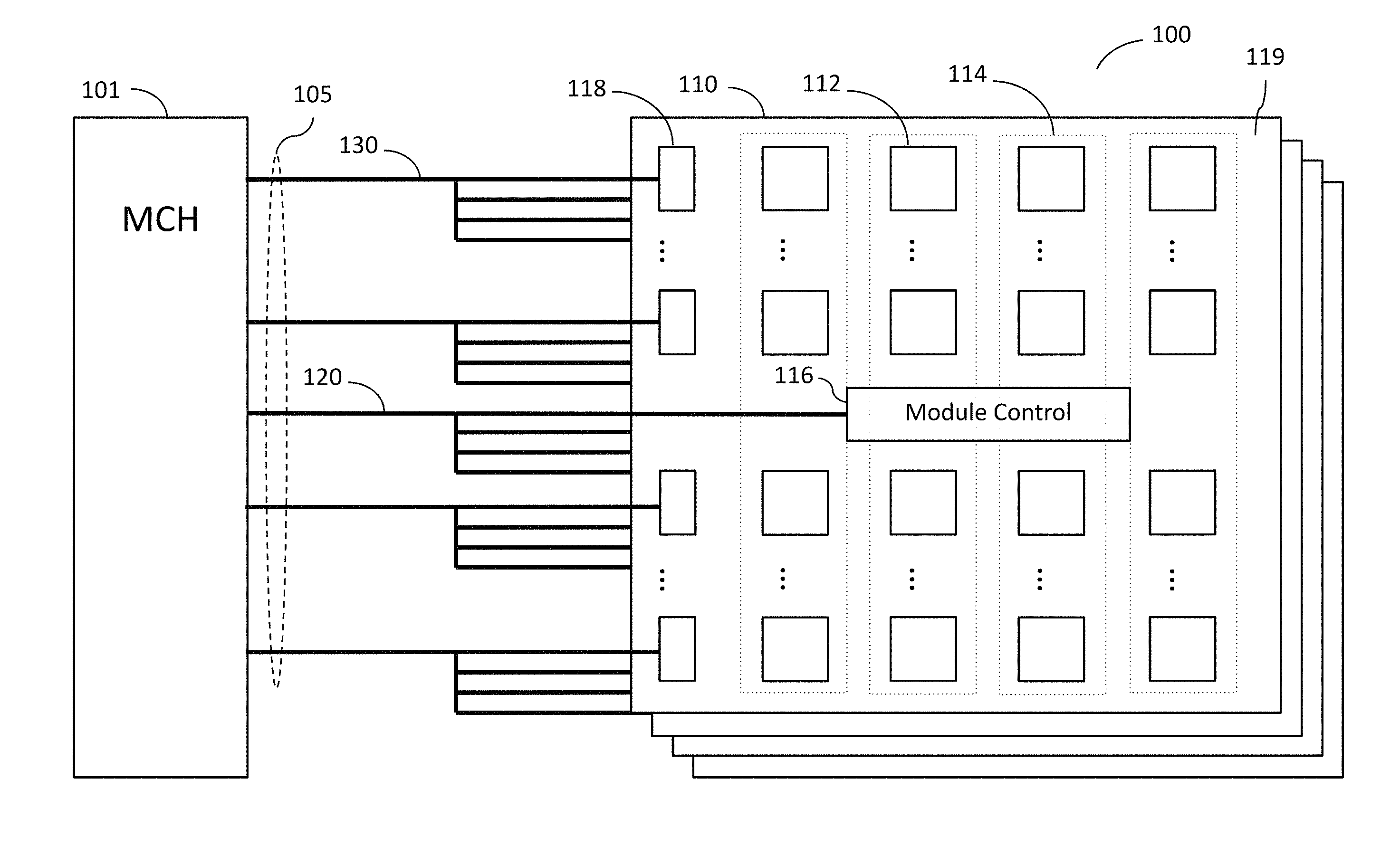
FIG. 1 shows a system 100 including a memory controller (MCH) 101 and one or more memory modules 110 coupled to the MCH by a memory bus 105, according to one embodiment. As shown, the memory bus includes C/A signal lines 120 and groups of system data/strobe signal lines 130. Also as shown, each memory module 110 has a plurality of memory devices 112 organized in a plurality of ranks 114. Each memory module 110 further includes a module control circuit (module controller or module control device) 116 coupled to the MCH 101 via the C/A signal lines 120, and a plurality of buffer circuits or isolation devices 118 coupled to the MCH 101 via respective groups of system data/strobe signal lines 130. In one embodiment, the memory devices 112, the module control circuit 116 and the isolation devices 118 can be mounted on a same side or different sides of a printed circuit board (module board) 119.
In the context of the present description, a rank refers to a set of memory devices that are selectable by a same chip select signal from the memory controller. The number of ranks of memory devices in a memory module 110 may vary. For example, as shown, each memory module 110 may include four ranks of memory devices 112. In another embodiment, the memory module 110 may include 2 ranks of memory devices. In yet another embodiment, the memory module may include six or more ranks of memory devices 112.
In the context of the present description, a memory controller refers to any device capable of sending instructions or commands, or otherwise controlling the memory devices 112. Additionally, in the context of the present description, a memory bus refers to any component, connection, or groups of components and/or connections, used to provide electrical communication between a memory module and a memory controller. For example, in various embodiments, the memory bus 105 may include printed circuit board (PCB) transmission lines, module connectors, component packages, sockets, and/or any other components or connections that provide connections for signal transmission.
Furthermore, the memory devices 112 may include any type of memory devices. For example, in one embodiment, the memory devices 112 may include dynamic random access memory (DRAM) devices. Additionally, in one embodiment, each memory module 110 may include a dual in-line memory module (DIMM).
Referring to FIG. 2A, which illustrates one memory module 110 according to an embodiment, the module control device 116 receives system memory commands represented by a set of system control/address (C/A) signals from the MCH 101 via signal lines 120 and generates module command signals and module control signals based on memory commands from the system. The module control device 116 also received a system clock MCK and generates a module clock signal CK in response to the system clock signal MCK. The MCK signal may include a pair of complementary clock signals, MCK and MCK, and the module clock signal may include a pair of complementary clock signals CK and CK.
Examples of the system C/A signals include, but are not limited to, Chip Select (or /CS) signal, which is used to select a rank of memory devices to be accessed during a memory (read or write) operation; Row Address Strobe (or /RAS) signal, which is used mostly to latch a row address and to initiate a memory cycle; Column Address Strove (or /CAS) signal, which is used mostly to latch a column address and to initiate a read or write operation; address signals, including bank address signals and row/column address signals, which are used to select a memory location on a memory device or chip; Write Enable (or /WE) signal, which is used to specify a read operation or a write operation, Output Enable (or /OE) signal, which is used to prevent data from appearing at the output until needed during a read operation, and the system clock signal MCK.
Examples of module command signals include, but are not limited to module /CS signals, which can be derived from the system /CS signals and one or more other system C/A signals, such as one or more bank address signals and/or one or more row/column address signals; a module /RAS signal, which can be, for example, a registered version of the system /RAS signal; a module /CAS signal, which can be, for example, a registered version of the system /CAS signal; module address signals, which can be, for example, registered versions of some or all of the address signals; a module /WE signal, which can be, for example, a registered version of the system /WE signal; a module /OE signal, which can be, for example a registered version of the system /OE signal. In certain embodiments, the module command signals may also include the module clock signal CK.
Examples of module control signals include, but are not limited to a mode signal (MODE), which specifies a mode of operation (e.g., test mode or operating mode) for the isolation devices 118; one or more enable signals, which are used by an isolation device to select one or more subgroups of memory devices to communicate data with the memory controller; and one or more ODT signals, which are used by the isolation devices to set up on-die termination for the data/strobe signals. In one embodiment, the module control signals are transmitted to the isolation devices 118 via respective module control signal lines 230. Alternatively, the module control signals can be packetized before being transmitted to the isolation devices 118 via the module control signal lines and decoded/processed at the isolation devices.
Module control device 116 transmits the module command signals to the memory devices 112 via module C/A signal lines 220. The memory devices 112 operate in response to the module command signals to receive write data or output read data as if the module command signals were from a memory controller. The module control device transmits the module control signals together with the module clock signal CK to the isolation devices 118 via module control signal lines 230. As shown in FIG. 2, at least some of the memory devices in a same rank share a same set of module C/A signal lines 220, and at least some of the isolation devices 118 share a same set of module control signal lines 230.
As shown n FIGS. 2A and 2B, each rank 114 includes N memory devices, where N is an integer larger than one. For example, a first rank includes memory devices M.sub.11, . . . , M.sub.i1, M.sub.i+1,1, . . . , M.sub.N, a second rank includes memory devices M.sub.12, . . . , M.sub.i2, M.sub.i+1,2, . . . , M.sub.N,2, and so on. In one embodiment, the memory devices 112 are also organized in groups or sets, with each group corresponding to a respective group of system data/strobe signal lines 130 and including at least one memory device from each rank. For example, memory devices M.sub.11, M.sub.12, M.sub.13, and M.sub.14 form a first group of memory devices, memory devices M.sub.i1, M.sub.i2, M.sub.i3, and M.sub.i4 form an i.sup.th group of memory devices, and so on.
As shown, the isolation devices 118 are associated with respective groups of memory devices and are coupled between respective groups of system data/strobe signal lines 130 and the respective groups of memory devices. For example, isolation device ID-1 among the isolation devices 118 is associated with the first group of memory devices M.sub.11, M.sub.12, M.sub.13, and M.sub.14 and is coupled between the group of system data/strobe signal lines 130-1 and the first group of memory devices, isolation devices ID-i among the isolation devices 118 is associated with the i.sup.th group of memory devices M.sub.i1, M.sub.i2, M.sub.i3, and M.sub.i4 and is coupled between the group of system data/strobe signal lines 130-i and the i.sup.th group of memory devices, and so on.
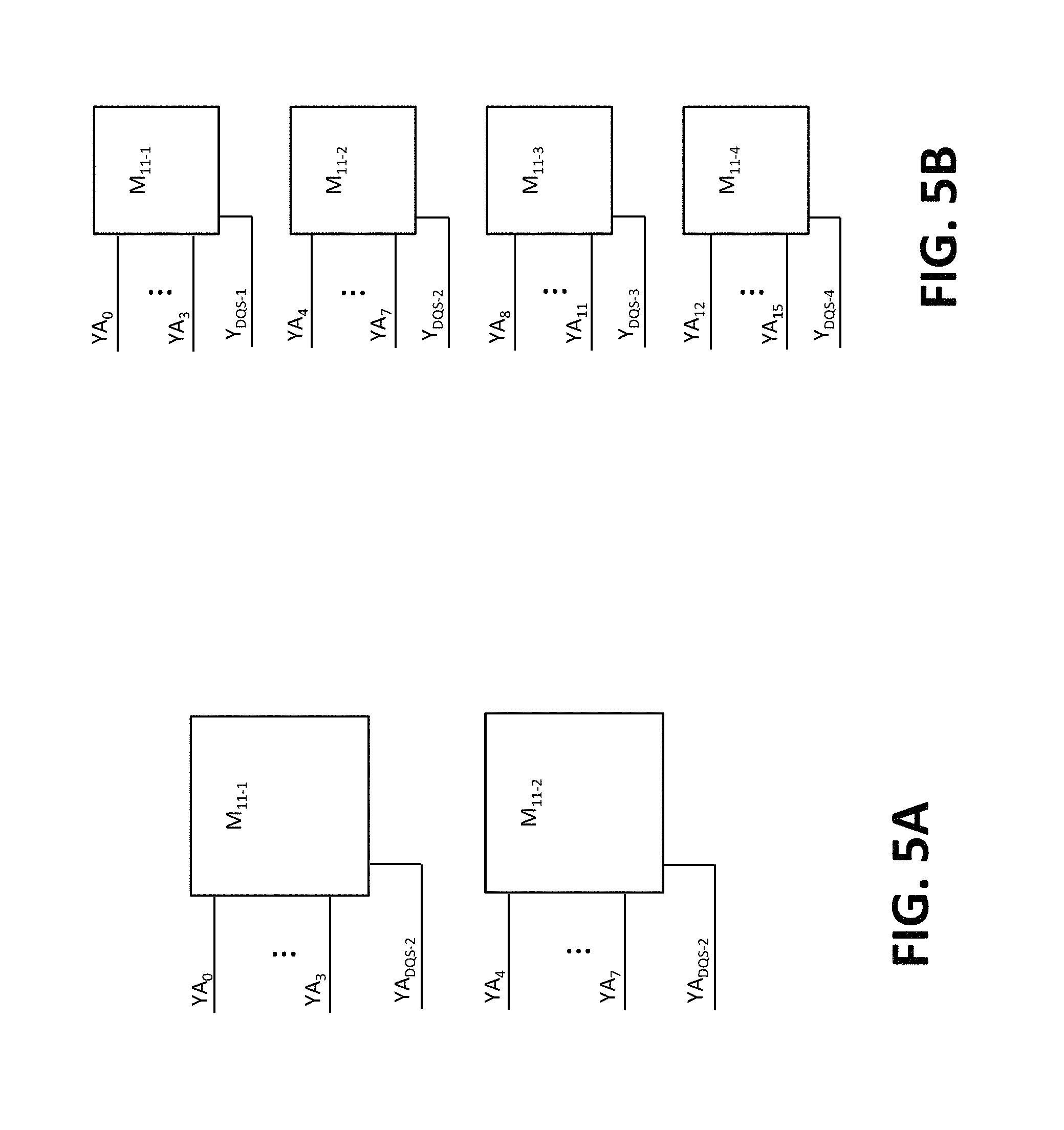
In one embodiment, each group or sets of memory devices are coupled to the associated isolation device 118 via a set of module data/strobe lines 210. Each group or set of memory devices is organized in subgroups or subsets, with each subgroup or subset including at least one memory device. The subgroups in a group of memory devices may be coupled to the associated isolation device 118 via a same set of module data/strobe lines 210 (as shown in FIG. 2A) or via respective subsets of module data/strobe lines 210 (as shown in FIG. 2B). For example, as shown in FIG. 2B, in the first group of memory devices, memory devices M.sub.11 and/or M.sub.13 form a first subgroup, and memory devices M.sub.12 and/or M.sub.14 form a second subgroup; in the i.sup.th group of memory devices, memory devices M.sub.i1 and/or M.sub.i3 form a first subgroup, and memory devices M.sub.i2 and/or M.sub.i4 form a second subgroup; and so on. The first subgroup of at least one memory device in each group of memory devices is coupled to the associated isolation device 118 via an associated first subset of module data/strobe lines YA, and the second subgroup of at least one memory device in each group of memory devices is coupled to the associated isolation device via an associated second subset of module data/strobe lines YB, as shown. For example, memory devices M.sub.11 and/or M.sub.13 form the first subgroup are/is coupled to the isolation device ID-1 via the corresponding first subset of module data/strobe lines YA-1, and memory devices M.sub.12 and/or M.sub.14 form the second subgroup are/is coupled to the isolation device ID-1 via the corresponding second subset of module data/strobe lines YA-2.
In one embodiment, the isolation devices 118 are in the data paths between the MCH 101 and the memory module 110 and include data buffers between the MCH 101 and the respective groups of memory devices. In one embodiment, each isolation device 118 is configured to select a subgroup in the respective group of memory devices to communicate data with the MCH 101 in response to the module control signals, such that the memory module can include more ranks than what is supported by the MCH 101. Further, each isolation devices 118 is configured to isolate unselected subgroup(s) of memory devices from the MCH 101 during write operations, so that the MCH sees a load on each data line that is less than a load associated with the respective group of memory devices. In one embodiment, the MCH sees only a load associated with one memory device on each data/strobe signal line during write operations.
In one embodiment, the isolation devices 118 are distributed across the memory module 110 or the module board 119 in positions corresponding to the respective groups of memory devices. For example, isolation device ID-1 is disposed in a first position corresponding to the first group of memory devices M.sub.11, M.sub.12, M.sub.13, and M.sub.14, and isolation device ID-i is disposed in an i.sup.th position separate from the first position and corresponding to the i.sup.th group of memory devices M.sub.i1, M.sub.i2, M.sub.i3, and M.sub.i4. In one embodiment, the first position is between the first group of memory devices and an edge 201 of the module board 119 where connections (not shown) to the data/strobe signal lines 130 are placed, and i.sup.th position is between the i.sup.th group of memory devices and the edge 201 of the module board 119. In one embodiment, the isolation devices 118 are distributed along the edge 201 of the memory module 110. In one embodiment, each isolation device 118 is a separate integrated circuit device packaged either by itself or together with at least some of the respective group of memory devices. In one embodiment, the module data/strobe signal lines 210, the module C/A signal lines 220, and the module control signal lines 230 include signal traces formed on and/or in the module board 119.
As an option, memory module 110 may further include a serial-presence detect (SPD) device 240, which may include electrically erasable programmable read-only memory (EEPROM) for storing data that characterize various attributes of the memory module 110. Examples of such data include a number of row addresses, a number of column addresses, a data width of the memory devices, a number of ranks on the memory module 110, a memory density per rank, a number of memory device on the memory module 110, and a memory density per memory device, etc. A basic input/output system (BIOS) of system 100 can be informed of these attributes of the memory module 110 by reading from the SPD 240 and can use such data to configure the MCH 101 properly for maximum reliability and performance.
In certain embodiments, the SPD 240 and/or the control circuit 116 store module configuration information, such as: memory space translation code, memory address mapping function code, input and output signals timing control information for the control circuit 116, input and output signals electrical and logical level control information for the control circuit 116, etc. In certain embodiments, the SPD 240 contains a system view of the module 110 which can be different from an actual physical construction of the module 110. For example, the SPD 240 stores at least one memory operation parameter that is different from a corresponding memory operation parameter in a system memory controller setting. The SPD 240 may also store at least on data buffer operation parameter that is different from a corresponding parameter in the system memory controller setting.
Thus, in certain embodiment, in the memory module 110, C/A signals representing a memory command are received and buffered by the module control circuit 116, so that the MCH sees only the module control circuit 116 as far as the C/A signals are concerned. Write data and strobe signals from the controller are received and buffered by the isolation devices 118 before being transmitted to the memory devices 112 by the isolation devices 118. On the other hand, read data and strobe signals from the memory devices are received and buffered by the isolation devices before being transmitted to the MCH via the system data/strobe signal lines 130. Thus, MCH 101 does not directly operate or control the memory devices 112. As far as data/strobe signals are concerned, the MCH 101 mainly sees the isolation devices 118, and the system 100 depends on the isolation devices 118 to properly time the transmission of the read data and strobe signals to the MCH 101.
In certain embodiments, the memory module 110 is a dual in-line memory module (DIMM) and the memory devices are double data rate (DDR) dynamic random access memory devices (DRAM). In certain embodiments, the control circuit 116 includes a DDR register, and logic for memory space translation between a system memory domain and a module level physical memory domain. Such translation may produce address mapping, proper interface timing for the control signals to the module level physical memory domain, and a proper interface electrical and logical level for the control signals to the module level physical memory domain.
As shown in FIG. 2C, in certain embodiments, the control circuit 116 transmits registered C/A and clock signals to the memory devices 112, and transmits module control signals and a registered clock signal (or module clock signal) to the isolation devices 118, in a fly-by configuration. As the speed of memory operations increase, issues can arise with respect to signal alignment for input, output delay variation due process, voltage and temperature (PVT) variations, synchronization with system memory controller interface, and phase drift accumulation during operation, etc. Electrical interface calibration drift during operation due to charge build up and timing interface calibration drift during operation due to environment change can also create issues.
For example, load reduction mechanism in the isolation devices 118 would provide a single data bus interface to the respective set of memory devices, which is hidden from the system memory controller 101. Thus, a long sequence of interface timing training may be required due to limited controllability of the system memory controller 101 over the interface between the memory devices 112 and the associated isolation devices 118. Furthermore, interface signal alignment-drift after the initial training would not be easily detected by the system memory controller 101, which may cause silent system failure.
Moreover, clock skew amongst the memory devices 112 and the associated isolation devices 118 due to the distributed architecture of the memory module 110 can cause synchronization issues. As the speed of memory operation increase, data period can become very close to the signal propagation delay time. Thus, such issues cannot simply be addressed by pipelining the data paths, as variation of the signal propagation time through I/Os becomes a very significant portion of a data period.
To address at least some of the above issues, in certain embodiments, as shown in FIG. 2D, the control circuit 116 transmits registered C/A signals to the memory devices 112, and transmits the module control signals and the module clock signal to the data buffers 118, in a fly-by arrangement. The memory devices 112 do not receive the module clock signal from the control circuit 116. Instead, each data buffer 118 regenerates the clock that is used by the respective set of memory devices 112. Each Data buffer 118 is thus responsible for providing a correct data timing interface between the respective set of memory devices 112 and the system memory controller 101. Each data buffer 118 is also responsible for providing the correct control signal timing between the control circuit 116 and the respective set of memory devices 112.
Thus, the memory module 110 in FIG. 2D allows a locally synchronized operation for each respective set of memory devices 112, which can correspond to a nibble or a byte of a DDR data bus between the memory module 110 and the system memory controller 101. Also, signal interface between each data buffer 118 and the respective set of memory devices 112 can be synchronized. In one embodiment, each data buffer 118 has a set of configurable operations, including, for example: programmable phase relationship between the clock it receives and the clock it regenerates, programmable phase adjustment for the data and data-strobe signals coupled to the memory devices 112, programmable phase adjustment for the data and data-strobe signals coupled to the system memory controller 101, programmable phase adjustment related to at least one control signal that is coupled to the control circuit 116. The locally synchronized operation also makes it easier for each data buffer 118 to perform self-testing of the associated set of memory devices 112, independent of the self-testing of other sets of memory devices performed by the other data buffers, as disclosed in commonly-owned U.S. Pat. No. 8,001,434, entitled "Memory Board with Self-Testing Capability," which is incorporated herein by reference in its entirety.
In certain embodiments, operations of the isolation devices 118 are controlled by the module control signals from the module control circuit 116, which generates the module control signals according to the C/A signals received from the MCH. Thus, the module control signals need to be properly received by the isolation devices 118 to insure their proper operation. In one embodiment, the module control signals are transmitted together with the module clock signal CK, which is also generated by the module control circuit 116 based on the system clock signal MCK. The isolation circuits 118 buffers the module clock signal, which is used to time the sampling of the module control signals. Since the isolation devices 118 are distributed across the memory module, the module control signal lines 230 can stretch across the memory module 110, over a distance of several centimeters. As the module control signals travel over such a distance, they can become misaligned with the module clock signal, resulting in metastability in the received module control signals. Therefore, in one embodiment, the isolation circuits 118 includes metastability detection circuits to detect metastability condition in the module control signals and signal adjustment circuits to adjust the module control signals and/or the module clock signal to mitigate any metastability condition in the module control signals, as explained in further detail below.
Because the isolation devices 118 are distributed across the memory module 110, during high speed operations, it may take more than one clock cycle time of the system clock MCK for the module control signals to travel along the module control signals lines 230 from the module control device 116 to the farthest positioned isolation devices 118, such as isolation device ID-1 and isolation device ID-(n-1) in the exemplary configuration shown in FIG. 2. In other words, a same set of module control signals may reach different isolation devices 118 at different times across more than one clock cycle of the system clock. For example, when the clock frequency of the system clock is higher than 800 MHz, the clock cycle time is less than about 1.2 ns. With a signal travel speed of about 70 ps per centimeter of signal line, a module control signal would travel about 15 cm during one clock cycle. When the clock frequency increases to 1600 MHz, a module control signal would travel less than 8 cm during one clock cycle. Thus, a module control signal line can have multiple module control signals on the line at the same time, i.e., before one module control signal reaches an end of the signal line, another module control signal appear on the signal line.
With the isolation devices 118 receiving module control signals at different times across more than one clock cycle, the module control signals alone are not sufficient to time the transmission of read data signals to the MCH 101 from the isolation devices 118. In one embodiment, each isolation devices includes signal alignment circuits that determine, during a write operation, a time interval between a time when one or more module control signals are received from the module control circuit 116 and a time when a write strobe or write data signal is received from the MCH 101. This time interval is used during a subsequent read operation to time the transmission of read data to the MCH 101, such that the read data follows a read command by a read latency value associated with the system 100, as explained in more detail below.
More illustrative information will now be set forth regarding various optional configurations, architectures, and features with which the foregoing framework may or may not be implemented, per the desires of the user. It should be strongly noted that the following information is set forth for illustrative purposes and should not be construed as limiting in any manner. Any of the following features may be optionally incorporated with or without the exclusion of other features described.
In one embodiment, as shown in FIG. 3, each group of signal lines 130 include a set of n data (DQ) signal lines 322 each for transmitting one of a set of data signals DQ.sub.0, DQ.sub.1, . . . , DQ.sub.n-1, and at least one strobe (DQS) signal line 324 for transmitting at least one strobe signal DQS. Each set of module data/strobe lines Y include a set of n module data signal lines Y.sub.0, Y.sub.1, . . . , Y.sub.n-1 and at least one module strobe signal line Y.sub.DQS. When the subsets of memory devices are coupled to the associated isolation device 118 via respective subsets of memory devices, each set of module data/strobe lines Y may include multiple subsets of module data/strobe lines, such as the subsets of module data/strobe lines YA and YB shown in FIG. 2B. Each subset of module data/strobe lines YA include a set of n first module data lines YA.sub.0, YA.sub.1, . . . , YA.sub.n and at least one first module strobe signal line YA.sub.DQS; and each subset of module data/strobe lines YB include a set of n second module data lines YB.sub.0, YB.sub.1, . . . , YB.sub.n and at least one second module strobe signal line YB.sub.DQS.
Each isolation device 118 includes a set of DQ routing circuits 320 coupled on one side to respective ones of the set of n DQ signal lines 322, and on another side to respective ones of the respective set of n module data lines, or respective ones of the respective subsets of module data lines, such as the first module data lines YA.sub.0, YA.sub.1, . . . , YA.sub.n and the second module data lines YB.sub.0, YB.sub.1, . . . , YB.sub.n. Each isolation device 118 further includes an ID control circuit 310 coupled on one side to the at least one DQS signal line 324, on another side to the one or more module strobe signal lines Y.sub.DQS, or the first module strobe signal line YA.sub.DQS and second module strobe signal line YB.sub.DQS. The ID control circuit 310 also receives the module clock signal CK and the module control signals via the module control signal lines 230, and outputs ID control signals 330 to the DQ routing circuits 320, including, for example, one or more enable signals ENA and/or ENB, and some or all of the other received, decoded, and/or otherwise processed module control signals, a delay signal DS, a read DQS signal RDQS, a write DQS signal WDQS, and a buffer clock signal CK0. Each DQ routing circuit 320 is configured to enable data communication between the respective DQ signal line 322 with a selected subgroup of one or more memory devices in response to the module control signals, as explained in more detail below.
In certain embodiments, the ID control circuit 310 also provides a delay signal DS, which is used by the DQ routing circuits 320 to align read data output by the isolation device 118 with read data output by the other isolation devices 118, as explained in further detail below. In certain embodiments, the ID control circuit 310 regenerates a clock signal from the module clock signal CK, which can have a programmable delay from the module clock signal. The regenerated clock signal is used as the clock signal CK0 and a clock signal CKM that is provided to the corresponding set of memory devices, as explained in more detail below.
The memory devices 112 are coupled to the isolation devices 118 via a same set of module data/strobe signal lines or different subsets of module data/strobe signal lines. For example, as shown in FIG. 4A, memory devices M.sub.11, M.sub.12, M.sub.13, and M.sub.14 in the first group of memory devices can be coupled to the isolation device ID-1 via a same set of module data lines Y-1.sub.0, Y-1.sub.1, . . . , Y-1.sub.n-1 and module strobe line Y-1.sub.DQS. In such embodiment, a subgroup in the group of memory devices can be selected by the isolation devices to communicated data with the MCH based on the phases of the data/strobe signals, which can be different with respect to different subgroups of memory devices.
Alternatively, as shown in FIG. 4B, memory devices M.sub.11 and M.sub.13, which form a subgroup in the first group of memory devices, are coupled to the isolation device ID-1 via the module data lines YA-1.sub.0, YA-1.sub.1, . . . , YA-1.sub.n and module strobe line YA-1.sub.DQS and memory devices M.sub.12 and M.sub.14, which form another subgroup in the first group of memory devices, are coupled to the isolation device ID-1 via the module data lines YB-1.sub.0, YB-1.sub.1, . . . , YB-1.sub.n and module strobe line YB-1.sub.DQS. Memory devices coupled to the same isolation devices can be disposed on a same side or different sides of the memory board 119. Memory devices coupled to the same isolation devices may be placed side by side, on opposite sides of the module boards 119, or stacked over each other, and/or over the associated isolation device.
Multiple memory devices having a data width that is less than a data width of the isolation devices 118 may be used in place of one of the memory devices 112, which has the same data width as that of the isolation devices. For example, as shown in FIG. 5A, two memory devices M.sub.11-1 and M.sub.11-2 may be used in place of the memory device M.sub.11. Each of the two memory devices M.sub.11-1 and M.sub.11-2 has a data width of 4, and together they act like a memory device M.sub.11 of a data width of 8. Thus, memory device M.sub.11-1 is coupled to the isolation device ID-1 via module data lines YA-1.sub.0, . . . , YA-1.sub.3 and module strobe line YA-1.sub.DQS-1 while memory circuit M.sub.11-2 is coupled to the isolation device ID-1 via module data lines YA-1.sub.4, . . . , YA-1.sub.7 and module strobe line YA-1.sub.DQS-2.
In another embodiment, as shown in FIG. 5B, four memory devices M.sub.11-1 to M.sub.11-4 may be used as the memory device M.sub.11. Each of the four memory devices M.sub.11-1 to M.sub.11-4 has a data width of 4, and together they act like a memory device M.sub.11 of a data width of 16. Thus, memory device M.sub.11-1 is coupled to the isolation device ID-1 via module data lines YA-1.sub.0, . . . , YA-1.sub.3 and module strobe line YA-1.sub.DQS-1 while memory device M.sub.11-2 is coupled to the isolation device ID-1 via module data lines YA-1.sub.4, . . . , YA-1.sub.7 and module strobe line YA-1.sub.DQS-2, and so on.
FIG. 6 illustrates the ID control circuit 310 in an isolation device 118. As shown, the ID control circuit 310 includes a clock buffer 610 to receive the module clock signal CK from the module control device 116, and to output a module clock signal CK0. The ID control circuit 310 further includes a strobe routing circuit 620 that are coupled on one side to the corresponding system DQS signal line 324 and on another side to the corresponding module DQS signal lines YA.sub.DQS and YB.sub.DQS. The ID control circuit 310 further includes a receiver circuit 630 with respect to each of at least some of the module control signals (MCS) to receive a respective one of the module control signals. The ID control circuit 310 further includes a command processing circuit 640 that provides the received, decoded, and/or otherwise processed module control signals 330 to the DQ routing circuits 320 and the strobe routing circuit 620 either directly or after further processing, if needed. The received/decoded/processed module control signals may include, for example, one or more enable signals ENA and/or ENB that are used by the DQ routing circuits 320 and the strobe routing circuit 620 to selectively enabling data communication between the MCH 101 and one of the subgroups in the respective group of memory devices, with which the isolation device is associated.
The strobe routing circuit 620 also buffers strobe signals received from either the MCH 101 or the memory devices 112, and output either a write strobe WDQS or read strobe RDQS to the DQ routing circuits 320. In one embodiment, the ID control circuit 310 further includes a delay control circuit 650 that receives one of the module control signals and either a data signal or a strobe signal and determines a delay amount to be used by the DQ routing circuit 320 and the strobe routing circuit 620. The delay amount is provided to the DQ routing circuit 320 and the strobe routing circuit in a delay signal DS.
In a receiver circuit 630, the respective MCS is received in accordance with the module clock signal CK0. In one embodiment, receiver circuit 630 samples the respective MCS using rising (or falling) edges of the module clock CK0. Since the isolation devices 118 are distributed across the memory module 110 at positions corresponding to the respective groups of memory devices, the module control signal lines 230 that carry the MCS to the isolation devices can stretch over a distance of more than 10 centimeters, as shown in FIG. 7. As the MCS and CK0 travel along their respective module control signal lines 710 and 720, they can become misaligned with each other when they reach the input pins 730 of an isolation device 118.
For example, a module control signal, like the MCS 810 shown in FIG. 8, can be perfectly aligned with the module clock signal CK, with a rising edge 801 of the module clock signal CK being at a center of a data eye 802, when the MCS signal and the clock signal leave the module control circuit 116. When the module control signal and the module clock signal reach an isolation device, however, their alignment can become shifted like the MCS 820 with respect to the CK signal, i.e., the rising edge 801 of the clock signal is near a left edge of a data eye of the MCS 820, barely providing enough set up time for proper sampling of the module control signal. Or, the module control signal, like the MCS 830, can be shifted with respect to the module clock signal such that a rising edge 801 of the clock signal is near a right edge of a data eye of the MCS, barely providing enough hold time for proper sampling of the module control signal. Or, ever worse, the module control signal, like the MCS 840, can be so shifted with respect to the module clock signal such that a rising edge 801 of the clock signal falls in the glitches 803 at the edge of a data eye of the MCS, meaning that the sampled results could be metastable.
In one embodiment, as shown in FIG. 9, a receiver circuit 630 includes a metastability detection circuit (MDC) 910 to determine a metastability condition in a corresponding module control signal MCS0. In one embodiment, the MDC 910 generates at least one delayed version of the module clock signal CK and at least one delayed version of the corresponding MCS0. The MDC 910 also generates one or more metastability indicators and outputs the one or more metastability indicators via lines 912 and/or 914.
The receiver circuit 630 further includes a signal selection circuit 920 that receives the module clock CK and the at least one delayed version of the module clock via signal lines 916. The signal selection circuit 920 also receives the corresponding MCS and the at least one delayed version of the corresponding MCS via signal lines 918. The signal selection circuit 920 selects a clock signal CK.sub.i from among the module clock CK and the at least one delayed version of the module clock based on one or more of the metastability indicators. The signal selection circuit 920 may also select an MCS signal MCS.sub.i from among the corresponding MCS and the at least one delayed version of the corresponding MCS based on at least one other metastability indicator.
The receiver circuit 630 further includes a sampler or register circuit 930 that samples the selected module control signal MCS.sub.i according to the selected clock signal CK.sub.i and outputs the sampled signal as the received module control signal, which is provided to the command processing circuit 640 for further processing (if needed) before being provided to the DQ routing circuits 320 and DQS routing circuit 620.
FIG. 10A illustrates an MDC 910 according to one embodiment. As shown, the MDC 910 includes a delay circuit 1012 that generates a delayed version MCS1 of the corresponding MCS0 by adding a predetermined amount of delay (e.g., 10 ps) to MCS0. MDC 910 also includes a delay circuit 1016 that generates a delayed version CK1 of the clock signal CK0 by adding a predetermined amount of delay to CK0. In one embodiment, CK1 is delayed from CK0 by about 1/10th of a clock cycle, e.g., 50-70 ps for an operating frequency of about 1600 MHz. The MDC 910 further includes a sampler circuit 1042 that samples MCS1 according to CK0 and outputs a sampled result A, a sampler circuit 1044 that samples MCS0 according to CK0 and outputs a sampled result B, and a sampler circuit 1046 that samples MCS0 according to CK1 and outputs a sampled result C. The MDC 910 further includes a logic circuit (e.g., a majority decision circuit) that generates metastability indicators Z1 and Z2 based on the sampled results A, B, and C.
In one embodiment, Z1 is the result of a logic operation (e.g., an XNOR operation) on the sampled result, e.g., Z1=A.sym.B, and Z2 is the result of another logic operation on the sampled results, e.g., Z2=B.sym.C. Thus, as shown in FIG. 10B and Table 1 below, when a metastability condition of insufficient hold time occurs, i.e., a rising clock edge 1061 of CK0 is close to the right side of a data eye where gliches at the edges of the data eyes can make C unpredicatable, A and B can be in agreement (i.e., Z1 is true) while B and C are likely not in agreement (i.e., Z2 is false). FIG. 10 C illustrates a metastability condition when there is insufficient set-up time. As shown in FIG. 10C and Table 1 below, a rising clock edge 1061 of CK0 is close to the left side of a data eye where gliches at the edges of the data eyes can make A unpredicatable. Thus, A and B can be in disagreement so Z1 is false while B and C can be in agreement so Z2 is true. Not shown in the figures is the situation that all A, B, and C are in agreement, meaning that both the rising clock edge 1061 of CK0 and the rising clock edge 1062 of CK1 are near the middle of an MCS0 data eye so there is no metastability issues and both Z1 and Z2 are true, as shown in Table 1.
FIG. 10D illustrates a signal selection circuit 920 according to an embodiment. As shown, in one embodiment, the signal selection circuit 920 includes a first multiplexor 1071 that selects between CK0 and CK1 based on the metastability indicator Z1, and a second multiplexor 1072 that selects between MCS0 and MCS1 based on the metastability indicator Z2. Thus, as shown in Table 1, where a metastability condition of insufficient hold time occurs, Z1=1 and Z2=0, and MCS1 is output from multiplexor 1071 while CK0 is output from multiplexor 1072. Sampler 930 thus samples MCS1 according to the rising edges of CK0. Thus, more hold time is provided to mitigate the metastability condition since MCS1 is shifted from MCS0 toward the right.
On the other hand, where a metastability condition of insufficient set-up time occurs, Z1=0 and Z2=1, and CK1 is output from multiplexor 1071 while MCS0 is output from multiplexor 1072. Sampler 930 thus samples MCS0 according to the rising edges of CK1. Since CK1 is shifted from CK0 toward the right, more set-up time is provided to mitigate the metastability condition.
TABLE-US-00001 TABLE 1 Metastability Detection and Signal Selection Sampler MS Output Indicators Signal Selection A B C Z1 Z2 MS Condition CK MCS D1 D1 D2 1 0 insufficient hold CK0 MCS1 time D1 D2 D2 0 1 insufficient set-up CK1 MCS0 time D1 D1 D1 1 1 no metastability CK0 MCS0
In the case when no metastability is detected, Z1=1 and Z2=1, and CK0 is output from multiplexor 1071 while MCS0 is output from multiplexor 1072. So, the unshifted module control signal is sampled according to the unshifted module clock signal.
FIGS. 10A-10D illustrate a relatively simple implementation of the metastability detection circuit (MDC) 910 where only three different sample points are provided to detect metastability condition in the module control signal. In general, the MDC 910 may generate more delayed versions of the module clock signal CK0 and/or the corresponding module control signal MCS0, and may include more sampler circuits to sample any additional delayed versions of the module control signal according to either the module clock signal or one of the delayed versions of the module clock signal. For example, as shown in FIG. 11A, the MDC 910 can include a plurality of delay circuits 1102 that generate m delayed versions of MCS0, e.g., MCS1, MCS2, . . . MCSm, and m delayed versions of CK0, e.g., CK1, CK2, . . . , CKm. The MDC 910 can include sampler circuits 1104 that sample MCS0 according to CK0, CK1, . . . , CKm, respectively, and sampler circuits 1104 that sample MCS0, MCS1, MCS2, . . . MCSm according to CK0, respectively. The outputs of the samplers 1104 are provided to a logic circuit 1120, which determines a metastability condition in MCK0 based on the sampler outputs using, for example, a majority decision logic. The logic circuit 1120 outputs a first metastability indicator on line(s) 912 and a second metastability indicator on line(s) 914.
FIG. 11B illustrates a signal selection circuit 920 according to an embodiment. As shown, in one embodiment, the signal selection circuit 920 includes a first multiplexor 1171 that selects between CK0, CK1, . . . , CKm based on the metastability indicator provided on line(s) 912, and a second multiplexor 1172 that selects between MCS0, MCS1, . . . , MCSm based on the metastability indicator provided on line(s) 914, such that the rising edges of the selected clock signal, e.g., Cki, are close to the middle of the respective data eyes in the selected module control signal, e.g., MCSi. The selected signals MCSi and Cki are provided to the sampler 930, which samples MCSi according to the rising edges of CKi.
As stated above, in certain embodiments, since the isolation devices 118 are in the data paths between the MCH 101 and the respective groups of memory devices 112, the MCH 101 does not have direct control of the memory devices 112. Thus, conventional read/write leveling techniques are not sufficient for managing read/write data timing. In one embodiment, the isolation devices 118 includes signal alignment mechanism to time the transmission of read data signals based on timing information derived from a prior write operation, as discussed further below.
FIG. 12A is a timing diagram for a write operation according to one embodiment. As shown, after a write command W/C associated with the write operation is received by the module control circuit 116 at time t1, the module control circuit 116 outputs one or more enable signals EN at time t2 in response to the write commands. The one or more enable signals are received by an isolation device 118 at time t3', which afterwards receives one or more strobe signal DQS from the MCH 101 at time t4. Note that the same enable signal may be received by another isolation device 118 at time t3', which can be in a different cycle of the system clock MCK from the cycle which t3 is in. The time interval between t4 and t1 is consistent with a write latency W.L. associated with the system 100, and is controllable by the MCH 101 and knowable to the isolation device 118. The time interval between t4 and t3, referred to hereafter as an enable-to-write data delay EWD, can be determined by the isolation device 118 since both these signals are received by the isolation device. Based on such determination, the isolation device 118 can have knowledge of the time interval between t3 and t1, referred to hereafter as a command-to-enable delay CED, which can be used by the isolation device 118 to properly time transmission of read data to the MCH, as explained further below.
FIG. 12B is a timing diagram for a read operation according to one embodiment. As shown, after a read command R/C associated with the read operation is received by the module control circuit 116 at time t5, the module control circuit 116 outputs one or more enable signals EN at time t6 in response to the read commands. The one or more enable signals are received by an isolation device 118 at time t7, which afterwards receives at time t8 read data signals (not shown) and one or more strobe signal DQS from the respective group of memory devices. Note that the same enable signal may be received by another isolation device 118 at time t3', which can be in a different cycle of the system clock MCK from the cycle which t3 is in. Thus, the enable signals alone cannot be used to time the transmission of the read signals by the isolation devices 118.
With knowledge of the time interval between t7 and t5, which should be about the same as the time interval between t3 and t1, i.e., the command-to-enable delay CED, in certain embodiments, the isolation device can add a proper amount of delay to the read data signals and the one or more DQS signal such that the read data signals and the one or more DQS signal are transmitted at time t9 by the isolation device to the MCH 101 via the respective group of data/strobe signal lines 130, with the time interval between t9 and t5 being consistent with a read latency R.L. associated with the system 100.
The time interval between t4 and t3, i.e., the enable to write data delay EWD, is determined by the delay control circuit 650 in the ID control circuit 310, as shown in FIG. 6. According to one embodiment, as shown in FIG. 13, the delay control circuit 650 includes a peramble detector 1310 to detect a write preamble in the DQS, a flip-flop circuit 1320 having an enable input EN receiving one of the module control signals and a clock input CK receiving the buffered module clock signal CK0, and a counter circuit 1330 having a Start input receiving the one of the module control signals, a Stop input receiving an output of the flip-flop circuit 1320. Thus, the output of the counter circuit, i.e., the delay signal DS, would indicate a time interval from when the write preamble is detected and when the one of the module control signal is received.
FIG. 14 illustrates a DQ or DQS routing circuit 320 or 620 according to an embodiment. As shown, the DQ/DQS routing circuit 320/620 includes a DQ/DQS pin 1401 that is coupled to the corresponding DQ/DQS signal line 322/324, a set of one or more DQS pins 1402 that is coupled to a corresponding module DQ/DQS line(s) Y/Y.sub.DQS, or YA/YA.sub.DQS and YB/YB.sub.DQS. The DQ/DQS routing circuit 320/620 further includes a write strobe buffer 1410 that buffers write data/strobe, and a write data/strobe receiver 1420 that samples the write data/strobe. The DQ/DQS routing circuit 320/620 further includes a plurality of write paths 1430 that are selectable or can be selectively enabled by one or more of the module control signals, such as the enable signals ENA and ENB.
The DQS routing circuit further includes a plurality of read paths 1450 that are selectable by the one or more of the module control signals. Output from the selected read path is delayed in a delay circuit 1460 by an amount controlled by the delay signal DS, and sampled by a sampler circuit 1470. The sampled read data/strobe is transmitted by transmitter 1480 onto the corresponding data/strobe signal line 322/324 via the DQ/DQS pin 1401.
FIG. 15 illustrates a DQS routing circuit 620 according to an embodiment. As shown, the DQS routing circuit 620 includes a first DQS pin 1501 that is coupled to a corresponding DQS signal line 324, a second DQS pin 1502A that is coupled to a corresponding module DQS line YA.sub.DQS, a third DQS pin 1502B that is coupled to a corresponding module DQS line YB.sub.DQS. The DQS routing circuit 620 further includes a first write strobe path coupled between the first DQS pin 1501 and the second DQS pin 1502A and a second write strobe path coupled between the first DQS pin 1501 and the third DQS pin 1502B. The first write strobe path includes a write strobe buffer 1510 that buffers a write strobe, a write strobe receiver 1520 that samples the write strobe according to the buffered module signal CK0. The sampled write strobe is provided to the DQ routing circuits 320 as the write strobe WDQS. The first write strobe path further includes a first write strobe transmitter 1530A that transmits the write strobe to one or more memory devices 112 coupled to the module strobe line YA.sub.DQS. The second write strobe path includes the write strobe buffer 1510, the write strobe receiver 1520, and a second write strobe transmitter 1530B that transmits the write strobe to one or more memory devices 112 coupled to the module strobe line YB.sub.DQS. The first and second write strobe transmitters, 1530A and 1530B, are controlled by two enable signals, ENA and ENB, respectively, such that the first write strobe path and the second write strobe path can be selectively enabled/disabled by the enable signals, ENA and ENB.
The DQS routing circuit further includes a read strobe path coupled between the first DQS pin 1501 and a selected one of the second and third DQS pins 1502A and 1502B. In the read strobe path, a select circuit 1550 (e.g., a multiplexor) selects either a read strobe signal received via DQS pin 1502A or a read strobe signal received via DQS pin 1502B based on one or both of the enable signals ENA or ENB. The selected read strobe signal is delayed in a delay circuit 1560 by an amount controlled by the delay signal DS, and sampled by a sampler circuit 1570 according to the buffered module clock signal CK0. The sampled read strobe is provided to the DQ routing circuits 320 as the read strobe RDQS and is transmitted by transmitter 1580 onto the corresponding strobe signal line 324 via the first DQS pin 1501.
FIG. 16 illustrates a DQ routing circuit 320 according to an embodiment. As shown, the DQ routing circuit 320 includes a first DQ pin 1601 that is coupled to a corresponding DQ signal line 130, a second DQ pin 1602A that is coupled to a corresponding module DQ line YA.sub.DQ, a third DQ pin 1602B that is coupled to a corresponding module DQ line YB.sub.DQ. The DQ routing circuit 320 further includes a first write data path coupled between the first DQ pin 1601 and the second DQ pin 1602A and a second write data path coupled between the first DQ pin 1601 and the third DQ pin 1602B. The first write data path includes a write data buffer 1610, a write data receiver 1620 that samples write data according to the write strobe WDQS from the DQS routing circuit 620, and a first write data transmitter 1630A that transmits the write data to one or more memory devices 112 coupled to the module data line YA.sub.DQ. The second write data path includes the write data buffer 1610, the write data receiver 1620, and a second write data transmitter 1630B that transmits the write data to one or more memory devices 112 coupled to the module data line YB.sub.DQ. The first and second write data transmitters, 1530A and 1530B, are controlled by two enable signals, ENA and ENB, respectively. Thus, the first write data path and the second write data path can be selectively enabled/disabled by the enable signals, ENA and ENB.
The DQ routing circuit further includes a read data path coupled between the first DQ pin 1601 and a selected one of the second and third DQ pins 1602A and 1602B. In the read data path, a select circuit 1650 (e.g., a multiplexor) selects either a read data signal received via DQ pin 1602A or a read data signal received via DQ pin 1602B based on one or both of the enable signals ENA or ENB. The selected read data signal is delayed in a delay circuit 1660 by an amount controlled by the delay signal DS. The delayed read data signal is then sampled by a receiver circuit 1670 according to the read strobe RDQS from the DQS routing circuit 620, and transmitted by transmitter 1680 onto the corresponding data signal line 130 via the first DQ pin 1601.
FIG. 17 illustrate a delay circuit 1560 or 1660 according to an embodiment. As shown, the delay circuit 1560 or 1660 includes a plurality of delay stages, such as delay stages 1710, 1720, and 1730, each delaying a read data or read strobe signal from the select circuit 1550/1650 by a predetermined amount. The delay circuit 1560 or 1660 further includes a select circuit 1740 (e.g., a multiplexor) that selects from among the read data or read strobe signal and the outputs from the delay stages according to the delay signal DS. The output of the select circuit 1740, is provided to the sampler circuit 1570 or 1670, either directly or after being buffered by a buffer circuit 1750.
Thus, as shown in FIG. 18, in one embodiment, a memory module 110 operates in the memory system 100 according to a method 1800. In the method, during a write operation, one or more module control signals are received by an isolation device 118 from a module control circuit or module controller 116 (1810). The module controller 116 generates the one or more module control signals in response to C/A signals representing a write command from the MCH 101. The one or more module control signals are used to control the isolation device 118. For example, the one or more module control signals may include one or more first enable signals to enable a write path to allow write data be communicated to a selected subgroup of memory devices among the group of memory devices coupled to the isolation device 118. After a time interval from receiving the one or more first enable signals, write data DQ and write strobe DQS are received by the isolation device 118 from the MCH 101 (1820). In one embodiment, upon receiving the one or more first enable signal, a counter is started, which is stopped when the write data DQ or write strobe DQS is received. Thus, a time interval EWD between receiving the one or more first enable signals and receiving the write strobe signal DQS is recorded.
Since the time interval between the arrival of the command signals from the MCH 101 and the arrival of the write data/strobe signal DQ/DQS from the MCH 101 is a set according to a write latency parameter associated with the system 100, the time interval EWD can be used to ascertain a time interval CED between the time when a command signal is received by the memory module 110 and the time when the one or more enable signals are received by the isolation device 118. The time interval CED can be used by the isolation device 118 to properly time the transmission of read data to the MCH 101, as described above and explained further below.
As shown in FIG. 18, a delay signal DS is generated according to the time interval EWD (1830). Concurrent to receiving the write strobe signal DQS, the isolation device 118 also receives a set of write data signals DQ (1840). The received write data signals are transmitted to the subgroup of memory devices (1850), which are selected from the group of memory devices coupled to the isolation device 118 by the one or more first enable signals.
During a read operation, another set of module control signals including, for example, one or more second enable signals, are received by the isolation device 118 from the module controller 116 (1860). The one or more second enable signals are generated by the module controller 116 in response to read command signals received from the MCH 101, and are used by the isolation device 118 to select a subgroup of memory devices from which to receive read data. Afterwards, a read strobe signal DQS and a set of read data signal DQ are received from the selected subgroup of memory devices (1870). To properly time the transmission of the DQS and DQ signals to the MCH 101, the DQS and DQ signals are adjusted (e.g., delayed) according to the delay signal DS, such that the DQS and DQ signals follow a read command by a time interval consistent with a read latency parameter associated with the system 100.
In certain embodiments, especially the embodiments shown in FIG. 2D, the delay circuits 1560 and 1660 shown in FIGS. 15 and 16 are not needed to provide alignment of the read data. As shown in FIG. 19, the ID control circuit 310 includes a clock regeneration circuit 1920 that regenerates the clock signal CK received from the control circuit 116, according to the delay signal DS. The regenerated clock signals CK0 and CKM each includes a proper amount of delay as compared to the clock signal CK. The clock CK0 is provided to the strobe routing circuit 620 so that the strobe signals are properly timed to result in proper data alignment. The regenerated clock signal CKM is provided to the respective set of memory devices so that the respective data buffer 118 and the respective set of memory devices are locally synchronized.
* * * * *
References
D00000
D00001
D00002
D00003
D00004
D00005
D00006
D00007
D00008
D00009
D00010
D00011
D00012

D00013

D00014

D00015

D00016
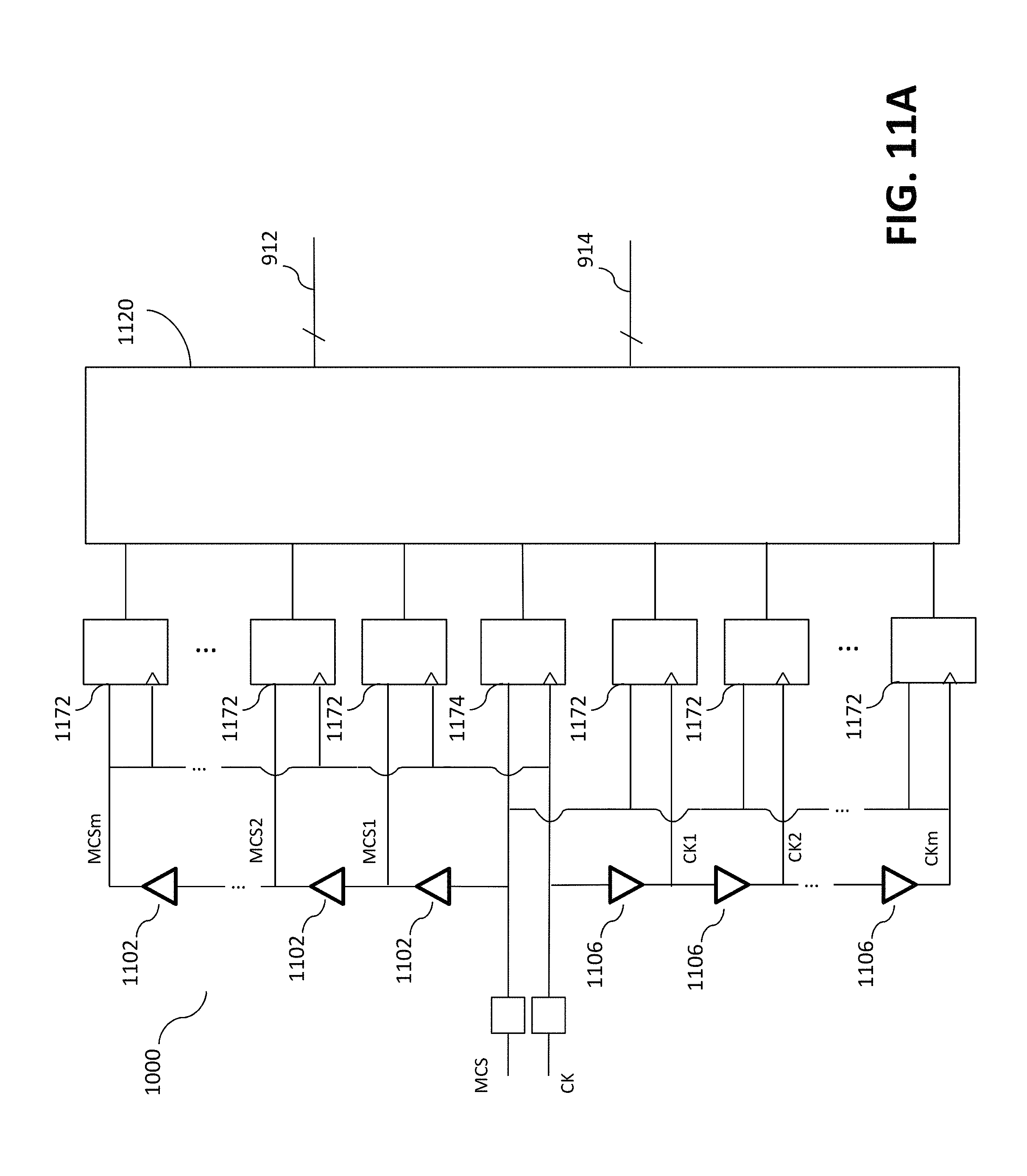
D00017

D00018

D00019

D00020

D00021

D00022

D00023

D00024

D00025

D00026

XML
uspto.report is an independent third-party trademark research tool that is not affiliated, endorsed, or sponsored by the United States Patent and Trademark Office (USPTO) or any other governmental organization. The information provided by uspto.report is based on publicly available data at the time of writing and is intended for informational purposes only.
While we strive to provide accurate and up-to-date information, we do not guarantee the accuracy, completeness, reliability, or suitability of the information displayed on this site. The use of this site is at your own risk. Any reliance you place on such information is therefore strictly at your own risk.
All official trademark data, including owner information, should be verified by visiting the official USPTO website at www.uspto.gov. This site is not intended to replace professional legal advice and should not be used as a substitute for consulting with a legal professional who is knowledgeable about trademark law.