Input member with capacitive sensor
Miller , et al.
U.S. patent number 10,262,179 [Application Number 15/585,074] was granted by the patent office on 2019-04-16 for input member with capacitive sensor. This patent grant is currently assigned to Apple Inc.. The grantee listed for this patent is Apple Inc.. Invention is credited to Jean-Marie Bussat, Tyler B. Cater, Sawyer I. Cohen, Steven P. Hotelling, Thayne M. Miller.


View All Diagrams
| United States Patent | 10,262,179 |
| Miller , et al. | April 16, 2019 |
Input member with capacitive sensor
Abstract
Input members with capacitive sensors are disclosed. In one embodiment of an electronic button, a first circuit is configured to capture a fingerprint of a user's finger placed on the electronic button, and a second circuit is configured to sense a force applied to the electronic button by the user's finger. The first circuit is further configured to provide temperature information to compensate for temperature sensitivities of the second circuit, and the second circuit is further configured to provide force information to the first circuit.
| Inventors: | Miller; Thayne M. (San Jose, CA), Bussat; Jean-Marie (San Jose, CA), Hotelling; Steven P. (Los Gatos, CA), Cohen; Sawyer I. (Menlo Park, CA), Cater; Tyler B. (San Jose, CA) | ||||||||||
|---|---|---|---|---|---|---|---|---|---|---|---|
| Applicant: |
|
||||||||||
| Assignee: | Apple Inc. (Cupertino,
CA) |
||||||||||
| Family ID: | 58778644 | ||||||||||
| Appl. No.: | 15/585,074 | ||||||||||
| Filed: | May 2, 2017 |
Prior Publication Data
| Document Identifier | Publication Date | |
|---|---|---|
| US 20170235403 A1 | Aug 17, 2017 | |
Related U.S. Patent Documents
| Application Number | Filing Date | Patent Number | Issue Date | ||
|---|---|---|---|---|---|
| 14340138 | Jul 24, 2014 | 9671889 | |||
| 61858606 | Jul 25, 2013 | ||||
| Current U.S. Class: | 1/1 |
| Current CPC Class: | H03K 17/962 (20130101); H03K 17/975 (20130101); G06K 9/0002 (20130101); H03K 2217/960755 (20130101) |
| Current International Class: | G06K 9/00 (20060101); H03K 17/96 (20060101); H03K 17/975 (20060101) |
| Field of Search: | ;382/124 |
References Cited [Referenced By]
U.S. Patent Documents
| 4527862 | July 1985 | Arakawa |
| 5343064 | August 1994 | Spangler et al. |
| 5929517 | July 1999 | Distefano et al. |
| 6002389 | December 1999 | Kasser |
| 6079282 | June 2000 | Lanter |
| 6154580 | November 2000 | Kuriyama et al. |
| 6323846 | November 2001 | Westerman et al. |
| 6545495 | April 2003 | Warmack et al. |
| 6568275 | May 2003 | Scholz et al. |
| 6570557 | May 2003 | Westerman et al. |
| 6570707 | May 2003 | Murakami |
| 6676611 | January 2004 | Bromba |
| 6677932 | January 2004 | Westerman |
| 6933031 | August 2005 | Ohta et al. |
| 6989728 | January 2006 | Van Zeeland et al. |
| 7158122 | January 2007 | Roberts |
| 7211885 | May 2007 | Nordal et al. |
| 7337085 | February 2008 | Soss |
| 7409876 | August 2008 | Ganapathi et al. |
| 7511702 | March 2009 | Hotelling |
| 7538760 | May 2009 | Hotelling et al. |
| 7609178 | October 2009 | Son et al. |
| 7719522 | May 2010 | Lyon et al. |
| 7784366 | August 2010 | Daverman et al. |
| 7800592 | September 2010 | Kerr et al. |
| 7920134 | April 2011 | Krah |
| 7920225 | April 2011 | Nishikawa et al. |
| 7946758 | May 2011 | Mooring |
| 8072437 | December 2011 | Miller et al. |
| 8111248 | February 2012 | Lee et al. |
| 8169332 | May 2012 | Bernstein et al. |
| 8169416 | May 2012 | Han |
| 8228306 | July 2012 | Long |
| 8253711 | August 2012 | Kim et al. |
| 8274495 | September 2012 | Lee |
| 8289290 | October 2012 | Klinghult |
| 8334849 | December 2012 | Murphy et al. |
| 8351993 | January 2013 | Nunes |
| 8390481 | March 2013 | Pance et al. |
| 8421978 | April 2013 | Wang et al. |
| 8436823 | May 2013 | Kanehira et al. |
| 8525797 | September 2013 | Liu et al. |
| 8547350 | October 2013 | Anglin et al. |
| 8577289 | November 2013 | Schlub et al. |
| 8577644 | November 2013 | Ksondzyk et al. |
| 8633916 | January 2014 | Bernstein et al. |
| 8638316 | January 2014 | Badaye et al. |
| 8669963 | March 2014 | Baker et al. |
| 8704787 | April 2014 | Yamamoto et al. |
| 8711122 | April 2014 | Wada et al. |
| 8724861 | May 2014 | Sun |
| 8743083 | June 2014 | Zanone et al. |
| 8760413 | June 2014 | Peterson et al. |
| 8780055 | July 2014 | Marchand et al. |
| 8780062 | July 2014 | Hibara et al. |
| 8780075 | July 2014 | Yamano et al. |
| 8810521 | August 2014 | Ito |
| 8830205 | September 2014 | Chang et al. |
| 8913031 | December 2014 | Honda et al. |
| 8922523 | December 2014 | Lynch et al. |
| 8963874 | February 2015 | Li et al. |
| 8970507 | March 2015 | Holbein et al. |
| 9001080 | April 2015 | Okayama et al. |
| 9007331 | April 2015 | Sobel et al. |
| 9024898 | May 2015 | Kim et al. |
| 9024907 | May 2015 | Bolender |
| 9030440 | May 2015 | Pope et al. |
| 9057653 | June 2015 | Schediwy et al. |
| 9086768 | July 2015 | Elias et al. |
| 9088282 | July 2015 | Holenarsipur et al. |
| 9092129 | July 2015 | Abdo et al. |
| 9104898 | August 2015 | Case |
| 9116569 | August 2015 | Stacy et al. |
| 9207134 | December 2015 | Ting et al. |
| 9229587 | January 2016 | Kawaguchi et al. |
| 9235645 | January 2016 | Ishizone et al. |
| 9262002 | February 2016 | Momeyer et al. |
| 9354752 | May 2016 | Kanehira et al. |
| 9375874 | June 2016 | Lin et al. |
| 9390308 | July 2016 | Mankowski et al. |
| 9411457 | August 2016 | Perlin et al. |
| 9411458 | August 2016 | Worfolk et al. |
| 9430102 | August 2016 | Prest et al. |
| 9454268 | September 2016 | Badaye et al. |
| 9459738 | October 2016 | Lin et al. |
| 9477342 | October 2016 | Daverman et al. |
| 9490804 | November 2016 | Hanumanthaiah et al. |
| 9494473 | November 2016 | Hanson et al. |
| 9535518 | January 2017 | Kang et al. |
| 9541578 | January 2017 | Shimata et al. |
| 9542589 | January 2017 | Thammasouk et al. |
| 9671889 | June 2017 | Miller et al. |
| 9678586 | June 2017 | Reynolds |
| 9710095 | July 2017 | Hotelling |
| 9715301 | July 2017 | Kuboyama et al. |
| 9772245 | September 2017 | Besling et al. |
| 9851828 | December 2017 | Richards et al. |
| 9910529 | March 2018 | Chang et al. |
| 2006/0197753 | September 2006 | Hotelling |
| 2007/0272919 | November 2007 | Mori et al. |
| 2008/0150901 | June 2008 | Lowles et al. |
| 2008/0309622 | December 2008 | Krah |
| 2009/0015564 | January 2009 | Ye et al. |
| 2009/0066345 | March 2009 | Klauk et al. |
| 2009/0237374 | September 2009 | Li et al. |
| 2010/0045628 | February 2010 | Gettemy et al. |
| 2010/0117989 | May 2010 | Chang |
| 2010/0123686 | May 2010 | Klinghult et al. |
| 2010/0220065 | September 2010 | Ma |
| 2011/0012845 | January 2011 | Rothkopf et al. |
| 2011/0037706 | February 2011 | Pasquero et al. |
| 2011/0080373 | April 2011 | Wang et al. |
| 2011/0096013 | April 2011 | Krumpelman et al. |
| 2011/0216016 | September 2011 | Rosener |
| 2011/0227872 | September 2011 | Huska et al. |
| 2011/0235156 | September 2011 | Kothari et al. |
| 2012/0038577 | February 2012 | Brown et al. |
| 2012/0056826 | March 2012 | Kim et al. |
| 2012/0086669 | April 2012 | Kim et al. |
| 2012/0089348 | April 2012 | Perlin et al. |
| 2012/0090757 | April 2012 | Buchan et al. |
| 2012/0092285 | April 2012 | Osborn et al. |
| 2012/0098760 | April 2012 | Chuang |
| 2012/0098767 | April 2012 | Takai et al. |
| 2012/0104097 | May 2012 | Moran et al. |
| 2012/0169612 | July 2012 | Alameh et al. |
| 2012/0188202 | July 2012 | Tsujino et al. |
| 2012/0229417 | September 2012 | Badaye et al. |
| 2012/0274602 | November 2012 | Bita et al. |
| 2012/0313863 | December 2012 | Hsu |
| 2012/0319987 | December 2012 | Woo |
| 2013/0076375 | March 2013 | Hanumanthaiah et al. |
| 2013/0113732 | May 2013 | Kang et al. |
| 2013/0128416 | May 2013 | Weber |
| 2013/0176270 | July 2013 | Cattivelli et al. |
| 2013/0285973 | October 2013 | Elias et al. |
| 2013/0328575 | December 2013 | Ra et al. |
| 2014/0085213 | March 2014 | Huppi et al. |
| 2014/0085247 | March 2014 | Leung et al. |
| 2014/0111953 | April 2014 | McClure et al. |
| 2014/0152621 | June 2014 | Okayama et al. |
| 2014/0176332 | June 2014 | Alameh |
| 2015/0071509 | March 2015 | Myers |
| 2015/0135108 | May 2015 | Pope et al. |
| 2015/0153829 | June 2015 | Shiraishi |
| 2015/0185909 | July 2015 | Gecnuk |
| 2015/0185946 | July 2015 | Fourie |
| 2015/0370376 | December 2015 | Harley et al. |
| 2015/0370396 | December 2015 | Ogata et al. |
| 2016/0033342 | February 2016 | Lyon et al. |
| 2016/0034088 | February 2016 | Richards et al. |
| 2016/0041648 | February 2016 | Richards |
| 2016/0042166 | February 2016 | Kang |
| 2016/0062498 | March 2016 | Huppi et al. |
| 2016/0070404 | March 2016 | Kerr et al. |
| 2016/0098131 | April 2016 | Ogata et al. |
| 2016/0103542 | April 2016 | Ogata et al. |
| 2016/0103544 | April 2016 | Filiz et al. |
| 2016/0139716 | May 2016 | Filiz et al. |
| 2016/0258981 | September 2016 | Bushnell et al. |
| 2016/0314334 | October 2016 | He et al. |
| 2016/0378255 | December 2016 | Butler et al. |
| 2017/0038877 | February 2017 | Kuboyama et al. |
| 2017/0046008 | February 2017 | Chen et al. |
| 2017/0285746 | October 2017 | Kim et al. |
| 2017/0322660 | November 2017 | Kuboyama et al. |
| 2018/0048058 | February 2018 | Ehman et al. |
| 2018/0069588 | March 2018 | Jiang et al. |
| 2018/0088702 | March 2018 | Shutzberg et al. |
| 2018/0138102 | May 2018 | Pan et al. |
| 2018/0275811 | September 2018 | Filiz et al. |
| 1502166 | Jun 2004 | CN | |||
| 1577385 | Feb 2005 | CN | |||
| 1582453 | Feb 2005 | CN | |||
| 1707415 | Dec 2005 | CN | |||
| 1714336 | Dec 2005 | CN | |||
| 101046720 | Oct 2007 | CN | |||
| 101207971 | Jun 2008 | CN | |||
| 101427468 | May 2009 | CN | |||
| 101673001 | Mar 2010 | CN | |||
| 101950224 | Jan 2011 | CN | |||
| 102016780 | Apr 2011 | CN | |||
| 201828892 | May 2011 | CN | |||
| 102103445 | Jun 2011 | CN | |||
| 102138120 | Jul 2011 | CN | |||
| 102193699 | Sep 2011 | CN | |||
| 102299166 | Dec 2011 | CN | |||
| 102365608 | Feb 2012 | CN | |||
| 102449583 | May 2012 | CN | |||
| 102467308 | May 2012 | CN | |||
| 102483673 | May 2012 | CN | |||
| 103221906 | Jul 2013 | CN | |||
| 204650590 | Sep 2015 | CN | |||
| 2073107 | Jun 2009 | EP | |||
| 2128747 | Dec 2009 | EP | |||
| 2237142 | Oct 2010 | EP | |||
| 2267791 | Dec 2010 | EP | |||
| 2315102 | Apr 2011 | EP | |||
| 2315186 | Apr 2011 | EP | |||
| 2357547 | Aug 2011 | EP | |||
| 2413224 | Feb 2012 | EP | |||
| 2418561 | Feb 2012 | EP | |||
| 2420918 | Feb 2012 | EP | |||
| 2508960 | Oct 2012 | EP | |||
| 2660688 | Nov 2013 | EP | |||
| 2708985 | Mar 2014 | EP | |||
| 2313195 | Nov 1997 | GB | |||
| S61292732 | Dec 1986 | JP | |||
| 2005031425 | Feb 2005 | JP | |||
| 2007310539 | Nov 2007 | JP | |||
| 2010225031 | Oct 2010 | JP | |||
| 2010244252 | Oct 2010 | JP | |||
| 2011100364 | May 2011 | JP | |||
| 2011134000 | Jul 2011 | JP | |||
| 2011197991 | Oct 2011 | JP | |||
| 2012064108 | Mar 2012 | JP | |||
| 2014052997 | Mar 2014 | JP | |||
| 1020070110114 | Nov 2007 | KR | |||
| 1020100074005 | Jul 2010 | KR | |||
| WO 97/018528 | May 1997 | WO | |||
| WO 11/081882 | Jul 2011 | WO | |||
| WO 11/156447 | Dec 2011 | WO | |||
| WO 12/031564 | Mar 2012 | WO | |||
| WO 12/147659 | Nov 2012 | WO | |||
| WO 12/160844 | Nov 2012 | WO | |||
| WO 13/083207 | Jun 2013 | WO | |||
| WO 13/183191 | Dec 2013 | WO | |||
| WO 14/018121 | Jan 2014 | WO | |||
| WO 12/153555 | Jul 2014 | WO | |||
| WO 14/124173 | Aug 2014 | WO | |||
Other References
|
Bau, et al., "TeslaTouch: Electrovibration for Touch Surfaces," UIST'10, Oct. 3-6, 2010, New York, New York USA, 10 pages. cited by applicant . Engineers Edge, Common Plastic Molding Design Material Specification, 2015, http://www.engineersedge.com/plastic/materials_common_plastic.htm, 3 pages. cited by applicant . Feist, "Samsung snags patent for new pressure sensitive touchscreens," posted on AndroidAuthority.com at URL: http://www.androidauthority.com/samsung-patent-pressure-sensitive-touchsc- reens-354860, Mar. 7, 2014, 1 page. cited by applicant . Widdle, "Measurement of the Poisson's ratio of flexible polyurethane foam and its influence on a uniaxial compression model," International Journal of Engineering Science, vol. 46, 2008, pp. 31-49. cited by applicant. |
Primary Examiner: Li; Ruiping
Attorney, Agent or Firm: Brownstein Hyatt Farber Schreck, LLP
Parent Case Text
CROSS-REFERENCE TO RELATED APPLICATION
This application is a continuation of U.S. patent application Ser. No. 14/340,138, filed Jul. 24, 2014, and entitled "Input Member with Capacitive Sensor," which claims the benefit under 35 U.S.C. .sctn. 119(e) of U.S. Provisional Patent Application No. 61/858,606, filed Jul. 25, 2013, entitled "Input Member with Capacitive Sensor," the contents of which are incorporated herein by reference as if fully disclosed herein.
Claims
What is claimed is:
1. A method of operating an electronic button, comprising: sensing, using a force sensor, a force applied to a surface of the electronic button; and correcting the sensed force using a temperature measurement; wherein a biometric sensor is configured to trigger the force sensor to sense the force responsive to human skin being detected by the biometric sensor.
2. The method of claim 1, wherein the sensed force takes one of a plurality of values, thereby representing a continuous measurement of force.
3. The method of claim 1, further comprising: determining that the sensed force exceeds a predefined level of force; and triggering capture of a biometric by the biometric sensor when the sensed force is determined to exceed the predefined level of force.
4. The method of claim 3, further comprising: notifying a user when the sensed force exceeds the predefined level of force.
5. The method of claim 1, further comprising: concentrating force using a force concentrator coupled between the biometric sensor and the force sensor; and translating motion of the biometric sensor into deflection of the force sensor using the force concentrator.
6. An electronic button, comprising: a first circuit configured to sense a force applied to a surface of the electronic button; a second circuit configured to capture a biometric on the surface of the electronic button; and a third circuit configured to combine an orientation of the captured biometric and the sensed force to provide three dimensional control of an electronic device.
7. The electronic button of claim 6, wherein the second circuit is configured to capture the biometric responsive to the sensed force being greater than a predefined force for biometric capture.
8. The electronic button of claim 6, wherein the first circuit comprises a strain gauge and the second circuit comprises a capacitive biometric sensor.
9. The electronic button of claim 6, wherein the electronic button is mechanically decoupled from a housing surrounding the electronic button.
10. The electronic button of claim 6, wherein the second circuit is mounted directly on the first circuit.
11. The electronic button of claim 6, wherein the second circuit is integrally included within a semiconductor die that also includes the first circuit.
12. A method of operating an electronic button, comprising: sensing, using a force sensor, a force applied to a surface of the electronic button; and capturing, using a biometric sensor, a biometric on the surface of the electronic button; and combining an orientation of the captured biometric and the sensed force to provide three dimensional control of an electronic device.
13. The method of claim 12, wherein the biometric sensor is configured to trigger the force sensor to sense the force responsive to human skin being detected by the biometric sensor.
14. The method of claim 12, further comprising determining, by a processor of the electronic button, whether the sensed force is within a range of forces at which the biometric can properly be captured.
15. The method of claim 12, wherein: sensing the force occurs over a period of time, resulting in two or more force values; and the method further comprises determining, by a processor of the electronic button, whether the two or more force values indicate that the force applied to the surface of the electronic button is stable over the period of time.
16. The method of claim 15, wherein capturing the biometric occurs responsive to determining that the two or more force values indicate that the force applied to the surface of the electronic button is stable over the period of time.
17. The method of claim 12, wherein the force sensor is further configured to trigger capturing a biometric responsive to sensing a predefined level of force applied to the surface of the electronic button.
18. The method of claim 12, further comprising adjusting, by a processor of the electronic button, the captured biometric based on the sensed force.
19. The electronic device of claim 6, wherein the first circuit is further configured to provide force information to the second circuit, and the second circuit is further configured to determine when to capture a biometric based on the force information provided by the first circuit.
20. The electronic device of claim 12, wherein the biometric sensor is configured to capture the biometric responsive to sensing the force.
Description
TECHNICAL FIELD
The present invention relates generally to electronic devices, and, more specifically, to input members with capacitive sensors for use in electronic devices.
BACKGROUND
Electronic devices in use today typically require input from a user in order to, for example, turn the electronic device on or complete some operation. A variety of different mechanisms are in place for receiving input from the user, such as a mechanical button. A mechanical button typically includes a body that is depressed by the user in order to complete an electrical circuit or otherwise trigger a reaction from the device. A restoring force then restores the button back to its original, non-depressed position, until the body is again depressed. Mechanical buttons such as these, however, typically consume a large amount of space in today's ever-slimming electronic devices. Furthermore, mechanical buttons such as these usually allow only for a binary output--indicating that the button is either depressed or is not depressed--and do not provide a smooth, continuous response. Such a smooth, continuous response is usually precluded by the structure of mechanical buttons as the depressed button either completes an electrical circuit or does not complete the circuit.
SUMMARY
In one aspect, an electronic button can include a first circuit configured to capture a fingerprint of a user's finger placed on the electronic button, and a second circuit configured to sense a force applied to the electronic button by the user's finger. In some embodiments, the first circuit is further configured to provide temperature information to compensate for temperature sensitivities of the second circuit, and the second circuit is further configured to provide force information to the first circuit. The first circuit may be configured to determine when to sense a fingerprint based on the force information provided by the second circuit. Additionally or alternatively, the first circuit can be configured to correct the captured fingerprint responsive to the sensed force being greater than a predefined acceptable force for fingerprint capture.
In other embodiments, the temperature information is provided to a third circuit, the third circuit being configured to correct the sensed force using the temperature information.
Additionally or alternatively, a third circuit configured to combine an orientation of the captured fingerprint and the sensed force to provide three dimensional control of an electronic device.
In another aspect, a method of operating an electronic button includes sensing a force applied to the electronic button using a force sensor, and correcting the sensed force using a temperature measurement. A fingerprint sensor is configured to trigger the force sensor to sense the force responsive to human skin being detected by the fingerprint sensor. The force sensor may be further configured to trigger capturing a fingerprint responsive to sensing a predefined level of force applied to the electronic button. In some embodiments, a user is notified when the sensed force exceeds a predefined level of force at which a fingerprint can be properly captured.
In yet another aspect, an electronic device includes an electronic button, where the electronic button includes a rigid body defining a beam and at least one opening adjacent the beam, and a strain gauge coupled to the rigid body. At least one portion of the strain gauge is mounted to the beam and sensitive to strain applied to a longitudinal axis of the beam.
In some embodiments, the electronic device also includes a capacitive fingerprint sensor configured to provide a temperature measurement to correct measurements from the strain gauge.
BRIEF DESCRIPTION OF THE DRAWINGS
FIG. 1A is a front view of an electronic device including an electronic button;
FIG. 1B is a graph showing a continuous response that may be provided by the electronic button of the electronic device of FIG. 1A;
FIG. 2 is a simplified block diagram of the electronic button of the electronic device in FIG. 1A;
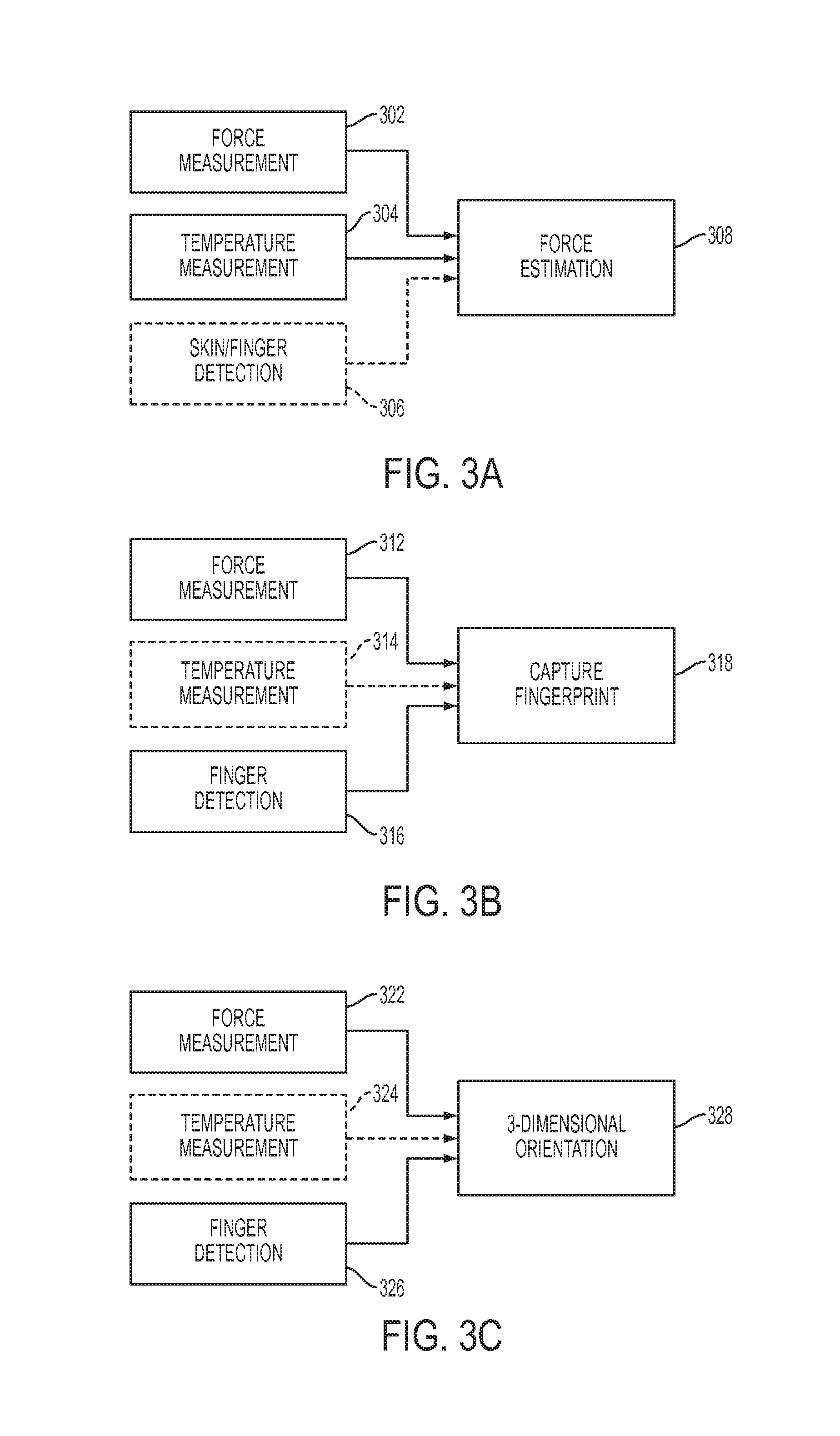
FIGS. 3A-3C are simplified flow diagrams illustrating several uses of the electronic button of the electronic device in FIG. 1A;
FIG. 4 is an exploded view of one embodiment of the electronic button of the electronic device in FIG. 1A;
FIG. 5 is a bottom view of the electronic button of the electronic device in FIG. 1A;
FIG. 6A is a cross-sectional view of the electronic button of the electronic device in FIG. 1A, taken along line H-H of FIG. 1A;
FIG. 6B is another cross-sectional view of the electronic button of the electronic device in FIG. 1A, taken along line V-V of FIG. 1A;
FIG. 7 is a simplified schematic view of a strain gauge of the electronic button of the electronic device in FIG. 1A;
FIG. 8 is a simplified schematic view of a capacitive fingerprint sensor of the electronic button of the electronic device in FIG. 1A;
FIG. 9 is an exploded view of a second embodiment of the electronic button of the electronic device in FIG. 1A;
FIG. 10 is a cross-sectional view of the electronic button of the second embodiment of the electronic button shown in FIG. 9;
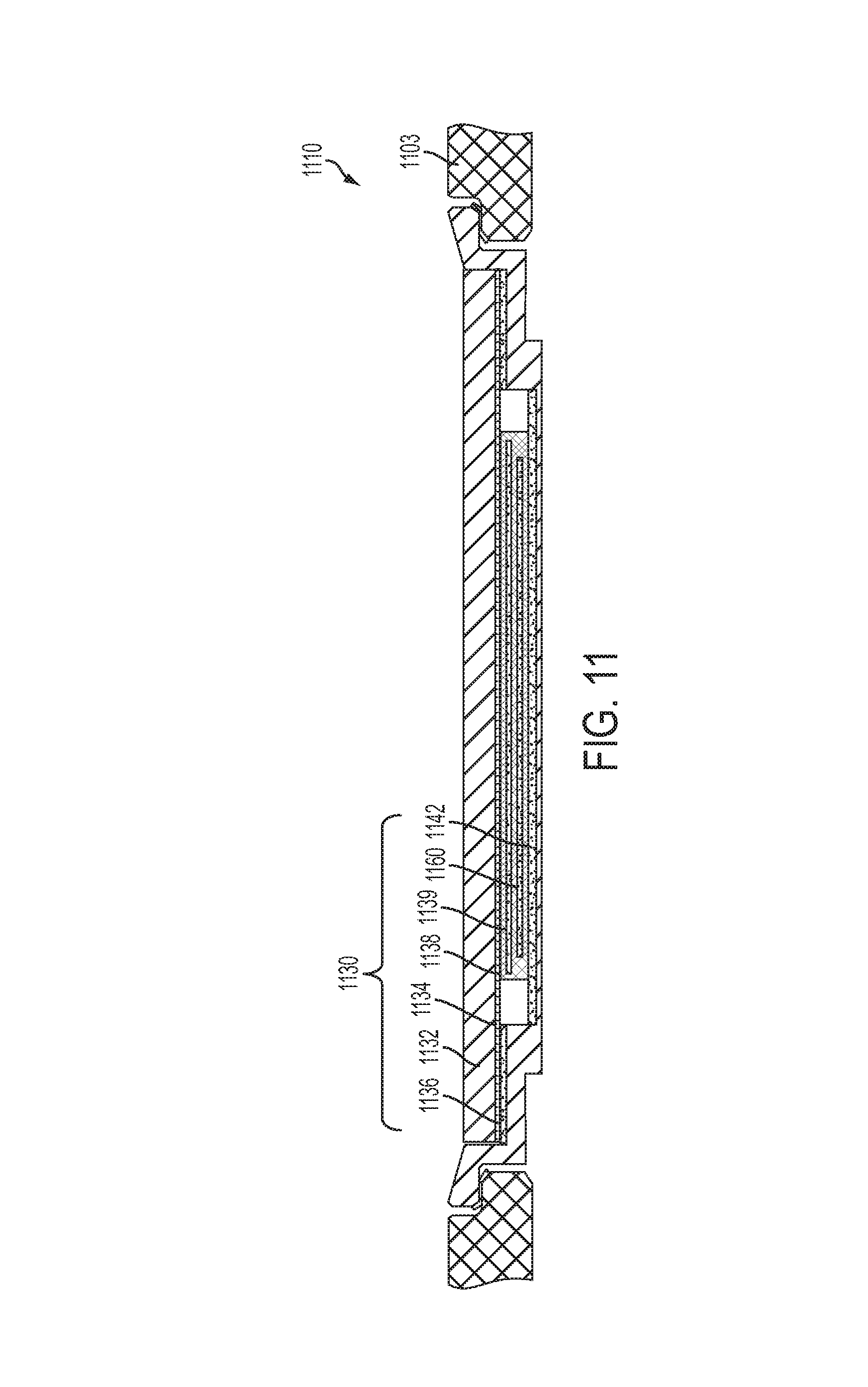
FIG. 11 is an exploded view of a third embodiment of the electronic button of the electronic device in FIG. 1A;
FIG. 12 is a cross-sectional view of another embodiment of an electronic button; and
FIGS. 13A and 13B are perspective and cross-sectional views of a button assembly.
DETAILED DESCRIPTION
Embodiments of an input member with a capacitive sensor, such as an electronic button, are described herein. FIG. 1A is a front view of an electronic device 100 including one or more electronic buttons 110. The electronic device 100 may be substantially any type of electronic or computing device, such as, but not limited to, a computer, a laptop, a tablet, a smart phone, a digital camera, a printer, a scanner, a copier, or the like. The electronic device 100 may also include one or more components typical of a computing or electronic device, such as, but not limited to, one or more processors, memory components, network interfaces, displays, cameras, and so on.
The electronic button 110 allows a user to interact with the electronic device 100. For example, the electronic button 110 may turn the electronic device 100 on, allow a user to perform some action such as returning to a home screen, and the like. The electronic device 100 may include more than one electronic button 110 in some embodiments, or may include only a single electronic button 110. The electronic device 100 may also include other input mechanisms, such as a mechanical button, multi-touch capacitive sensing display screen, one or more input/output ports, and so forth.
The electronic button 110 may in some embodiments be mechanically decoupled (e.g., isolated) from a housing 103 that surrounds the button 110 on one or more sides of the electronic button 110, or be decoupled from another part of the body of the electronic device 100. In other embodiments, the electronic button 110 may not be mechanically decoupled from the housing 103 or body (e.g., may be mechanically coupled to the housing 103), or may only be partially decoupled from the housing 103 or body. For example, in some embodiments, the housing 103 may be a glass plate, in which case one or more portions of the electronic button 110 may be integral with the glass plate.
As mentioned above, although not explicitly shown in FIG. 1A, the electronic device 100 may include a number of internal components, such as one or more processors, a storage or memory component, an input/output interface, a power source, and one or more sensors. The one or more processors may control operation of the electronic device 100 (including the electronic button 110 as described herein), and may individually or collectively be in communication with substantially all of the components of the electronic device 100. The processor may be any electronic device cable of processing, receiving, and/or transmitting instructions. As described herein, the term "processor" is meant to encompass a single processor or processing unit, multiple processors, or multiple processing units, or other suitably configured computing element.
FIG. 1B illustrates a graph demonstrating the response of an electronic button, such as the electronic button 110 illustrated in FIG. 1A, that has a continuous response to varying levels of force applied to the button. As used herein, continuous refers to a measurement that can take more than two values--for example, a measurement of force that can take one of five, ten, twenty, fifty, a hundred, a thousand, or tens of thousands of different values. The electronic button 110 in FIG. 1A may have a continuous response to applied forces, as compared with a mechanical button, which may only be on or off.
FIG. 2 is a simplified block diagram of one embodiment of the electronic button 110 of the electronic device 100 in FIG. 1A. The electronic button 110 in FIG. 2 includes a first circuit 130 and a second circuit 160. The first circuit 130 may be configured to capture a fingerprint of a user's finger placed on the electronic button 110. The first circuit 130 may include, for example, a capacitive fingerprint sensor. The first circuit 130 may also include one or more temperatures sensors embedded within or positioned external to the first circuit.
The second circuit 160 may be configured to sense a force applied to the electronic button 110 by the user's finger. The second circuit 160 may include, for example, a strain gauge, a capacitive gap sensor, and so forth. In some embodiments, such as when the second circuit 160 is a strain gauge, the second circuit 160 may be susceptible to temperature variations such that the force measurements provided by the second circuit 160 depend not only on the displacement of the electronic button 110, but also on the ambient temperature around the second circuit 160 or on the temperature of the components of the second circuit 160 themselves. The temperature of the components of the second circuit 160 may change in some embodiments as a result of, for example, the heat from a user's finger and/or the heat from the first circuit 130 operating, if the first and second circuits 130, 160 are positioned in proximity to one another.
In some embodiments, and as illustrated in FIG. 2, the first circuit 130 may be configured to provide temperature information to compensate for temperature sensitivities of the second circuit 160. This information may be used by the second circuit 160 to compensate for the temperature dependency of the force measurements. In some examples, the temperature information from the first circuit 130 may be provided to a third circuit (not illustrated in FIG. 2). Such a third circuit may also receive the raw force measurement from the second circuit 160, and may correct such raw force measurements using the temperature information. In other words, while the temperature information from the first circuit 130 may in some examples be provided directly to the second circuit 160 for the second circuit 160 itself to correct for the temperature dependency of the force measurements, in other examples, the temperature information from the first circuit 130 may be combined with the raw force information from the second circuit 160 in a separate, third circuit, such as a processor, to correct for the temperature distortions.
As also illustrated in FIG. 2, the second circuit 160 may be configured to provide force information to the first circuit 130 in some embodiments. The force information from the second circuit 160 may be feedback to the first circuit 130 in order to better understand a fingerprint captured by the first circuit 130. For example, if a user applies a relatively large amount of force to the electronic button 110, the fingerprint captured by the first circuit 130 may be distorted, or otherwise different than if the user had applied a normal amount of force. Similarly, if not enough force is used to press the electronic button 110, the ridges and valleys of the fingerprint may not be properly captured by the fingerprint button 110. The first and second circuits 130, 160, optionally together with a third circuit (not shown), can thus work together to allow a shallower electronic button 110 to be used in an electronic device 100 in place of a conventional mechanical button. The feedback between the first and second circuits 130, 160 of the electronic button 110 enables the cooperation of the first and second circuits 130, 160.
Turning now to FIGS. 3A through 3C, flowcharts are shown illustrating a few examples of how the electronic button 110 may be used in operation.
With reference to FIG. 3A, the electronic button 110 may in some examples be configured to estimate an actual force applied to the electronic button 110. Specifically, the force measurement 302 from the second circuit 160 may be combined with the temperature measurement 304 from the first circuit 130 in order to provide an estimated force 308 with which the electronic button 110 was depressed. Using the estimated force 308, the electronic button 110 may be able to correct a fingerprint captured using the first circuit 130 if, for example, the sensed force 302 is greater than a predefined acceptable force for fingerprint capture, as also explained in more detail below.
In some embodiments, and still with reference to FIG. 3A, the electronic button 110 may be configured to trigger the second circuit 160 to sense the force applied to the electronic button 110 responsive to human skin (e.g., a finger, palm, etc.) being detected by the first circuit 130. In order to conserve power, for example, the second circuit 160 may not continuously measure the force applied to the electronic button 110, but instead may only activate the sensing circuitry of the second circuit 160 if human skin or a finger is detected on the electronic button. In another embodiment, the second circuit 160 may continuously measure the force applied to the electronic button 110, but may signal a "click" to the electronic device 100 only in the event that a human finger or other portion of human skin is detected on the electronic button 110. This may reduce accidental activation of the electronic button 110, particularly when the electronic button 110 is not decoupled from one or more other portions of the electronic device 100, but also when the electronic button is decoupled from one or more other portions of the electronic device 100. This may reduce the likelihood that the electronic button 110 would signal a click activation if a pen in a user's pocket accidentally depresses the button. In still other embodiments, however, the second circuit 160 may continuously measure the force applied to the electronic button 110, and provide the same to the electronic device 100, regardless of whether human skin or a human finger is detected by the first circuit 130.
With reference to FIG. 3B, the electronic button 110 may in some examples be configured to determine when to sense a fingerprint based on the force information provided by the second circuit 160. Specifically, the force measurement 312 from the second circuit 160 may be combined with a finger detection indication 316 from the first circuit 130 to provide an indication 318 that triggers the first circuit 130 to capture the fingerprint of the user. In some examples, a temperature measurement 314 from the first circuit 130 may optionally be used during this process in order to, for example, correct the force measurement 312 provided by the second circuit 160 for temperature distortions.
In one example, if the force measurement 312 from the second circuit 160, as optionally corrected using the temperature measurement 314, is within a range of forces at which a fingerprint can be properly captured, the indication 316 may be provided to the first circuit 130 in order to capture the fingerprint. If, on the other hand, the force measurement 312 from the second circuit 160, as optionally corrected using the temperature measurement 314, is below a predefined level of force, the electronic button 110 may cause the electronic device 100 to request that the user try again, pressing more firmly on the electronic button 110. If, however, the sensed force 312 from the second circuit 160, as optionally corrected using the temperature measurement 314, exceeds a predefined level of force at which a fingerprint can be properly captured, the electronic button 110 may cause the electronic device 100 to request that the user try again, pressing less firmly on the electronic button 110.
In still other examples, the force measurements 312 may be used in other manners. For example, the force measurements 312 may be monitored such that when the force applied to the electronic button 110 is relatively stable (e.g., is not rapidly varying), the indication 318 is given to capture the fingerprint. Alternatively, the force measurement 312 may be used by the electronic button 1110 to compensate for the effect of too much or too little force being used to press the button 110--for example, if too much force is used, and the force measurement 312 reflects this excess, an algorithm may be applied to a fingerprint that is nonetheless captured by the first circuit 130 in order to compensate for the distortions in the captured fingerprint caused by the excess force. If, for example, the excess force causes the ridges of a fingerprint to be more spaced out and the valleys of the fingerprint to be wider, the force measurement 312 representative of the force applied to the electronic button 110 at that time may be used to adjust the width of the valleys and the spacing of the ridges.
In some embodiments, the force sensing accomplished by the second circuit 160 may consume less power and generate less heat than the fingerprint capturing of the first circuit 130, and thus it may be more economical to measure the force applied to the electronic button 110 at a relatively high sample rate, and only capture a fingerprint when a sufficient, but not excessive, force is applied to the electronic button 110. The first circuit 130 may nonetheless operate in a limited fashion, for example it may obtain and provide the temperature measurement 314 in order to adjust the force measurements 312 from the second circuit 1160 during operation, without necessarily activating the components of the first circuit 130 that actually function to capture the fingerprint (e.g., the capacitive sensing aspects of the first circuit 130).
With reference to FIG. 3C, the electronic button 110 may in some examples be configured to provide a 3-dimensional orientation of a user's finger that is used to depress the electronic button 110. Specifically, the force measurement 322 from the second circuit 160 may be combined with a finger detection indication 326 from the first circuit 130 in order to provide the 3-dimensional orientation 328--e.g., the first circuit 130 may provide vertical and horizontal orientation of the finger using the fingerprint ridges and valleys, while the second circuit 160 may provide the depth aspect of the 3-dimensional orientation. The 3-dimensional orientation 328 provided by the electronic button 110 may be used, for example, to control the electronic device 100--such as controlling a character or other object in a game, or otherwise controlling the navigation within the electronic device 100.
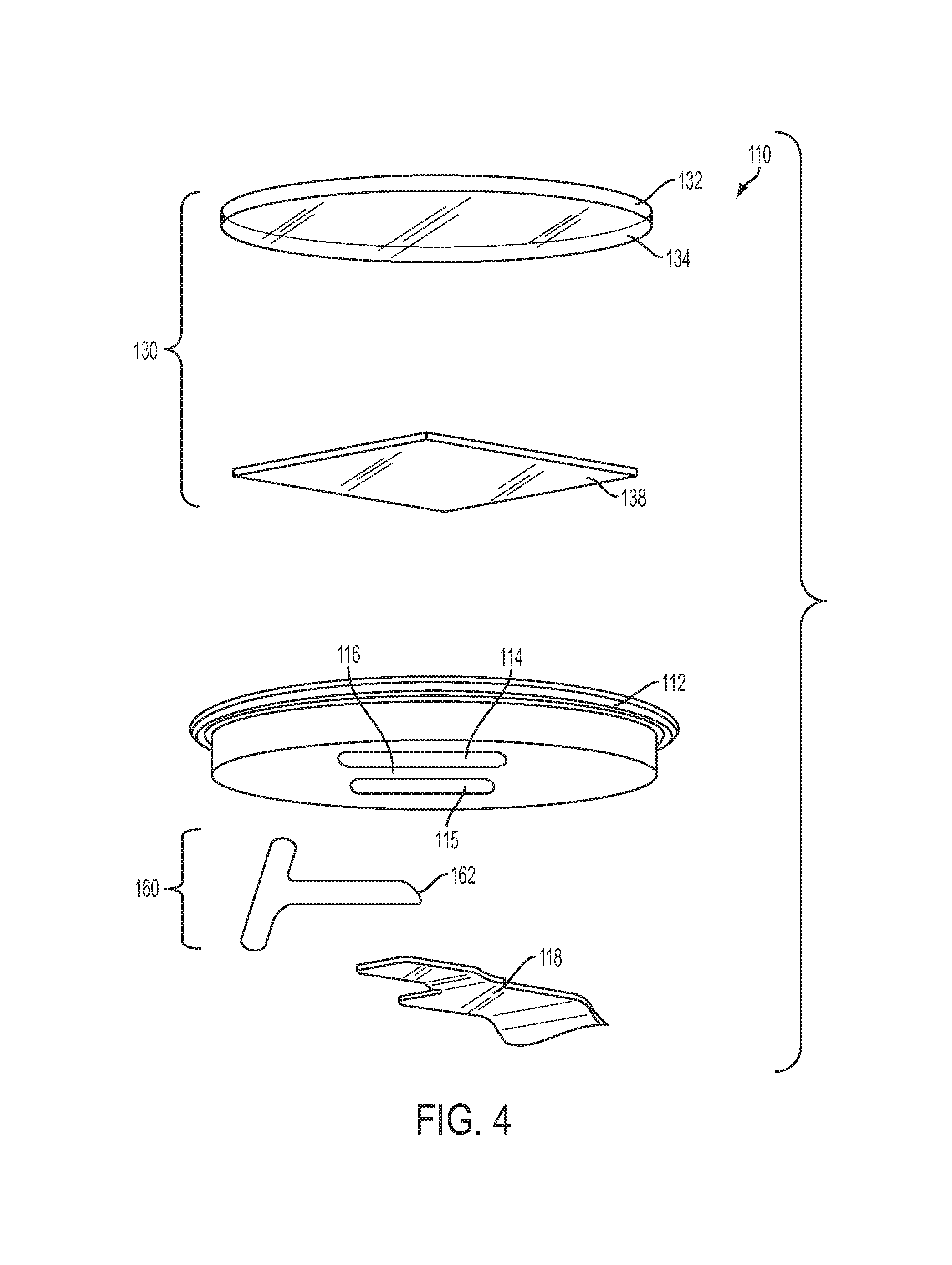
With reference now to FIG. 4, an exploded view of one embodiment of an electronic button 110 is shown. The electronic button 110 includes a first circuit 130 and a second circuit 160, similar to those shown in FIG. 2 and described above.
The first circuit 130 includes a cylindrical member 132, which may include sapphire, glass, and so forth. The cylindrical member 132 may include a layer of ink 134 positioned on the bottom of the cylindrical member 132. The first circuit 130 also includes a capacitive fingerprint sensor 138, which may be embodied in a silicon die with circuitry for detecting and capturing a fingerprint, circuitry for sensing human skin, temperature sensors, and so forth.
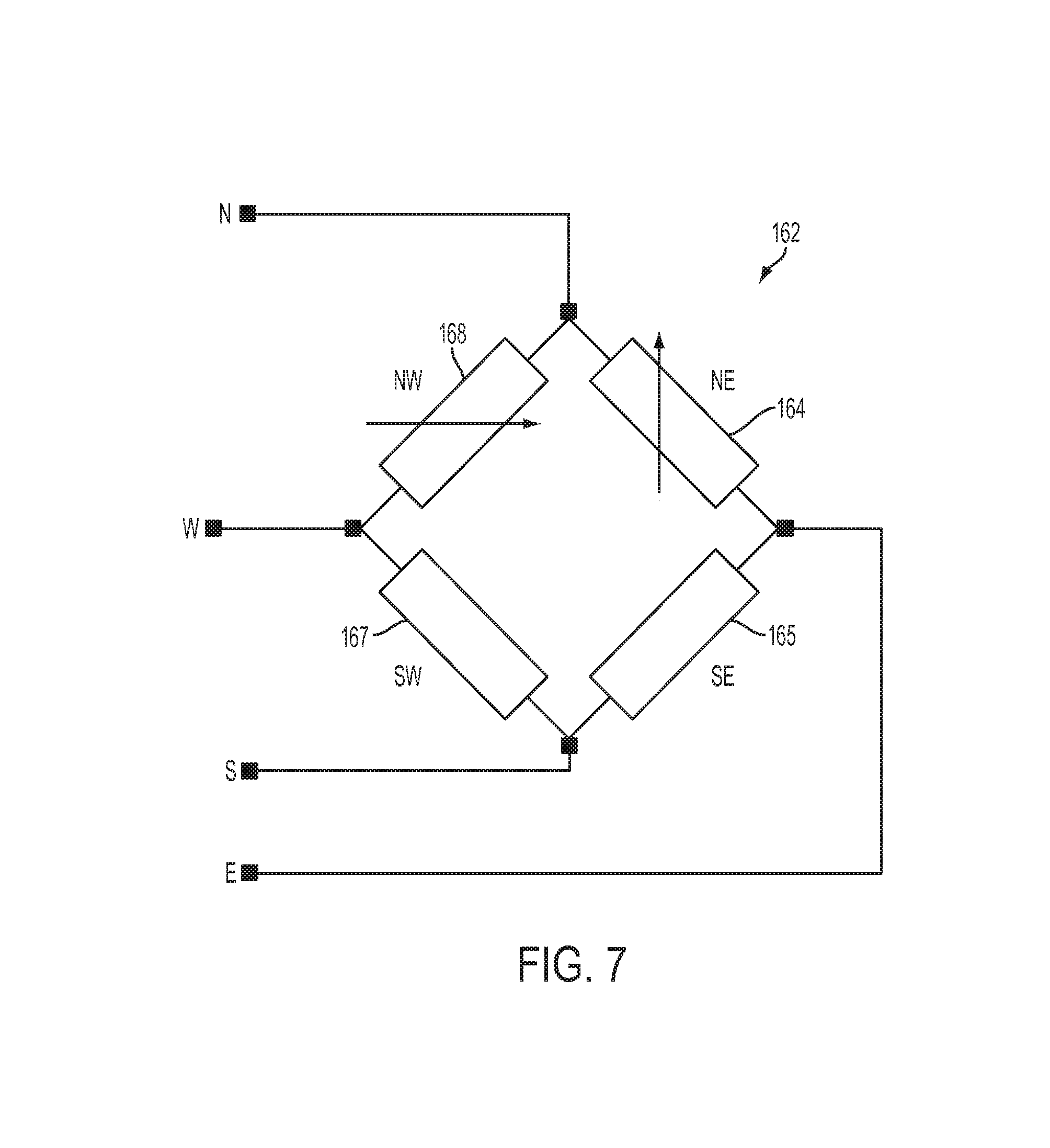
The electronic button 110 also includes a second circuit 160, which may include a strain gauge 162. The strain gauge 162 may generally define a T-shape, and may in some embodiments include four gauge components 164, 165, 166, 167, as explained in more detail below. The four gauge components 1164, 165, 166, 167 may together form a full-bridge, in order to thermally and electrically match the strain gauge 162.
The electronic button also includes trim 112, which may generally have a ring shape, and may be coupled between the first and second circuits 130, 160. The trim 112 may be a rigid body (comprised, for example, of stainless steel or another hard material), and may define a beam 116 and one or more openings 114, 115 adjacent the beam. As illustrated in FIG. 4, the capacitive fingerprint sensor 138 may be positioned on an opposite side of the trim 112 from the strain gauge 162, as described in more detail below with reference to FIG. 6A, in order to provide thermal insulation and/or electrical shielding between the strain gauge 1162 and the capacitive fingerprint sensor 138.
The electronic button 110 may also include a flex circuit 118 configured to be coupled to the first and second circuits 130, 160, and to route signals from the first and second circuits 130, 160 to a processor or other portion of the electronic device 100.
As illustrated in 4, the electronic button 110 may be mechanically decoupled from a housing 103 surrounding the electronic button 110; however in other embodiments, one or more components of the electronic button 110 (e.g., cylindrical member 132) may be integral with the housing 103 of the electronic device 100.
With reference to FIG. 5, which is a bottom view of the embodiment of an electronic button 110 shown in FIG. 4, the strain gauge 162 of the second circuit 160 may be coupled to the rigid body of the trim 112. More specifically, in one example, an elongated trunk of the T-shaped strain gauge 162 including NE and SE gauge components 164, 165 may be mounted to the beam 1116 of the trim 112. One or more of the NE, SE gauge components 164, 165 may be sensitive to strain applied to a longitudinal axis of the beam. In this example, NE gauge component 1164 may be sensitive to strain applied to the longitudinal axis of the beam, whereas SE gauge component 165 may be sensitive to strain applied to the vertical axis of the beam. Due to their proximity to one another and their common location on the beam 116, the NE gauge component 164 and the SE gauge component 165 may both be subject to similar temperature variations. Thus, the NE gauge component 164 is sensitive to strain applied along the horizontal axis of the beam 116 and also to temperature variations, while the SE gauge component 165 is not sensitive to strain applied along the horizontal axis of the beam 116 but is sensitive to temperature variations. Signals generated by the SE and NE gauge components 164, 165 can thus be combined in order to provide a first level of temperature correction, however the temperature sensors in the first circuit 130 can further be used to compensate for the temperature sensitivities of the strain gauge 162.
Still with reference to FIG. 5, NW and SW gauge components 166, 167 of the strain gauge 162 may also be coupled to the rigid body of the trim 112, but they may not be sensitive to displacement of the electronic button 110. Instead, the NW, SW gauge components 166, 167 may be used to electrically match the NE, SE gauge components 164, 165.
As mentioned above, the trim 112 may include one or more openings 114, 115, which may facilitate communication of signals between the strain gauge 162 and the capacitive fingerprint sensor 138, and also may allow a single flex circuit 118 to be used to route signals from both the strain gauge 162 and the capacitive fingerprint sensor 138 to another location of the electronic device 100, such as a processor. As illustrated for example in FIG. 5, a plurality of through silicon vias (TSVs) 120 of the capacitive fingerprint sensor 138 may be positioned near one of the openings 115 in the trim 112, such that signals E, N, S, W from the strain gauge 162 may be provided to the capacitive fingerprint sensor 138 and also to the flex circuit 118. Signals from the capacitive fingerprint sensor 138 may also be provided to the strain gauge 162 and/or to the flex circuit 118 through the one or more openings 114, 115, as shown in FIG. 5. In other words, the flex circuit 118 may be coupled to the capacitive fingerprint sensor 138 through the opening 115 of the trim 112 and also coupled to the strain gauge 162.
As illustrated in FIG. 5, one or more components of the strain gauge 162 may be adjusted. For example, region 158 in FIG. 5 illustrates a region 158 where one or more strain gauge 162 components can be laser trimmed in order to provide electrical matching between two or more portions of the strain gauge, in order for the strain gauge to properly function as a full bridge with good cancellation. The region 158 may be trimmed after the strain gauge 162 is mounted to the trim 112 in some examples.
As also illustrated in FIG. 5, in some examples, the NW, SW gauge components 1166, 167 may be interdigitated in order to increase the thermal and strain matching.
FIG. 6A illustrates a cross-sectional view of the electronic button 1110 shown in FIGS. 4 and 5, taken along line H-H of FIG. 1A, and FIG. 6B illustrates a cross-sectional view of the electronic button 110 shown in FIGS. 4 and 5, taken along line V-V of FIG. 1A. With reference to both FIGS. 6A and 6B, the cylindrical member 132 and ink layer 134 are coupled to the trim 112 via adhesive 136. The ink layer 134 is also coupled to the capacitive fingerprint sensor 138 through adhesive 140, and the capacitive fingerprint sensor 138 is coupled to the trim 112 through adhesive 142. The strain gauge 162 is coupled to the beam 116 of the trim 112 through adhesive 161. Also, flex circuit 118 is coupled to one or more TSVs of the capacitive fingerprint sensor 138 through adhesive 144, and trim 112 is moveable within housing 103 via shim member 104.
As can be seen in FIGS. 6A and 6B, the trim 112 allows some separation between the capacitive fingerprint sensor 138 and the strain gauge 162. Such separation may provide a thermal buffer and/or an electrostatic shield between the capacitive fingerprint sensor 138 and the strain gauge 162. The trim 112, however, provides stiffness, with the beam 116 dissipating some of the pressure applied to the electronic button 110, and the openings 114, 115 in the trim facilitating communication of signals and measurements between the first and second circuits 130, 160.
FIG. 7 illustrates a full bridge, including all of the NE, SE, SW, NW components 164, 165, 166, 167 of the strain gauge 162. The full bridge strain gauge 162 provides many benefits, including helping eliminate errors due to the flex circuit 118 and wire or trace bond connection resistances. In other embodiments, however, a quarter or half bridge could be used with a single or only two components of a strain gauge 162, in which case the first circuit can still provide temperature correction information in order to correct the temperature dependency of the measurements of force by the strain gauge 162.
FIG. 8 illustrates a top view of a capacitive fingerprint sensor 138 of the first circuit 130, with a plurality of different quadrants 139-A, 139-B, 139-C, 139-D, 139-E, 139-F, 139-G, 139-H, 139-I. In some embodiments, each of the plurality of quadrants 139-A, 139-B, 139-C, 139-D, 139-E, 139-F, 1139-G, 1139-H, 139-I includes one or more temperatures sensors.
The layout of the capacitive fingerprint sensor 138 may be such that its various components are arranged in order to provide a substantially uniform temperature gradient of the capacitive fingerprint sensor adjacent the beam 116 of the trim 112. So, for example, relatively "cool" digital components of the capacitive fingerprint sensor 138 may be positioned in quadrants 1139-F, 1139-G, 139-H, and 139-I so that the temperature gradient along those quadrants is minimized. In another example, the "warm" analog components of the capacitive fingerprint sensor 138 may be evenly distributed among quadrants 139-F, 139-G, 139-H, and 139-I in order to reduce the temperature gradient therealong.
Minimizing the temperature gradient along the NE and SE components 164, 165 of the strain gauge 162 may allow the SE component 165 to better cancel out the thermal dependency of the NE component 164, because both SE, NE components 164, 165 will be subjected to similar thermal conditions. If, on the other hand, quadrants 139-F and 139-G were much warmer or much cooler than quadrants 139-H, 139-I, the effectiveness of the thermal cancelation between the NE and SE components 164, 165 of the strain gauge 162 may be reduced.
As mentioned above, and with reference still to the quadrants 139-A, 139-B, 139-C, 139-D, 139-E, 139-F, 139-G, 139-H, 139-I illustrated in FIG. 8, one or more temperature sensors may be included in each of the quadrants 139-A, 139-B, 139-C, 139-D, 139-E, 139-F, 139-G, 139-H, 139-I in order to, for example, measure and correct for any temperature gradient that nonetheless exists in the capacitive fingerprint sensor 138.
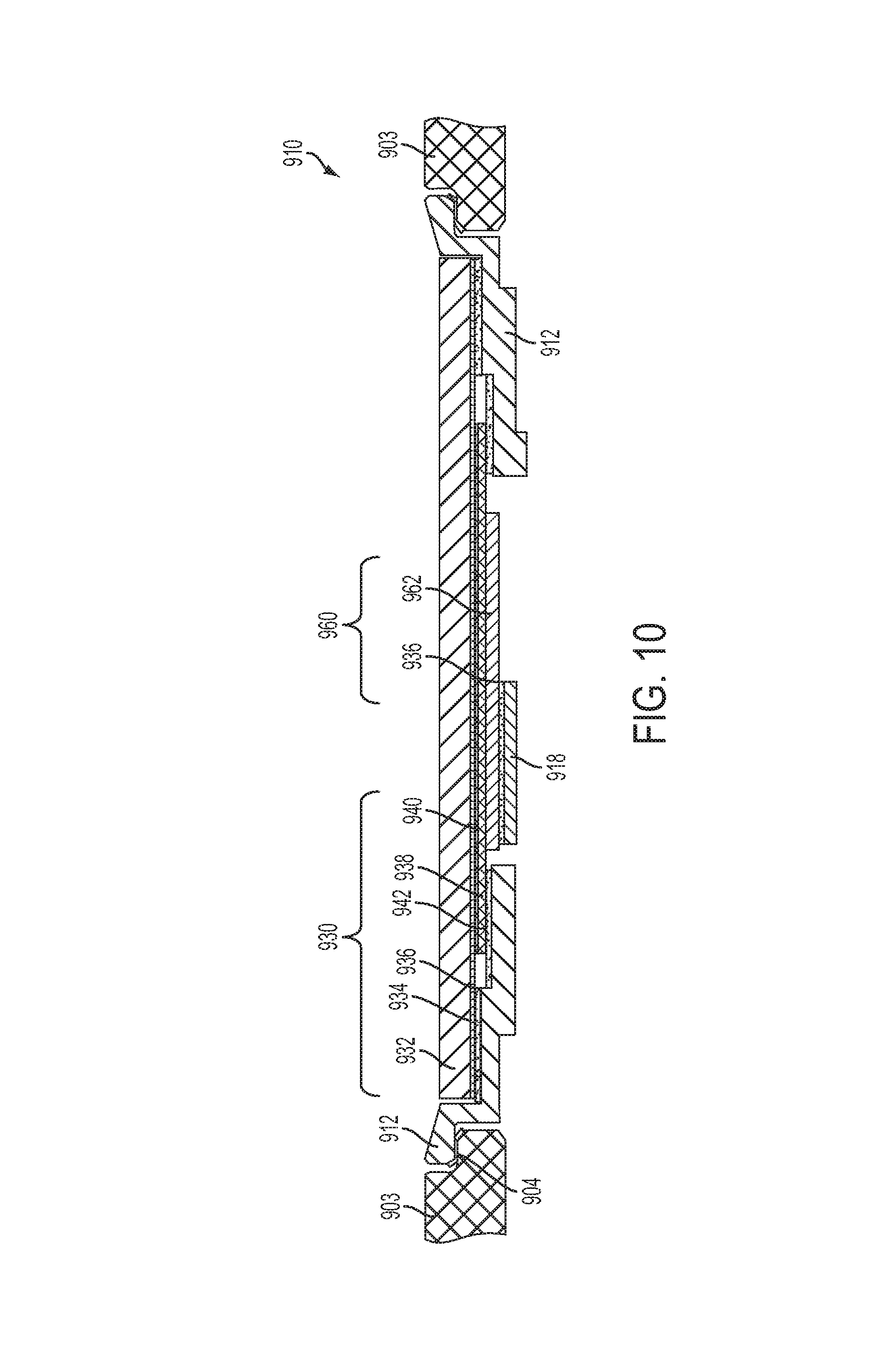
With reference to FIGS. 9 and 10, another embodiment of an electronic button 910 is shown. The electronic button 910 illustrated in FIGS. 9 and 10 is similar to the electronic button 110 shown and described above, except that the strain gauge 962 is mounted directly to the capacitive fingerprint sensor 938.
With reference to FIG. 11, another embodiment of an electronic button 1110 is shown. The electronic button 1110 illustrated in FIG. 11 is similar to the electronic button 110 shown and described above, except that the second circuit 1160 (including the strain gauge, for example) is integrally included within a semiconductor die that also includes capacitive fingerprint sensor 1139. In this manner, a single semiconductor die can include circuitry for performing the functions of both the first and second circuits 130, 160 described above.
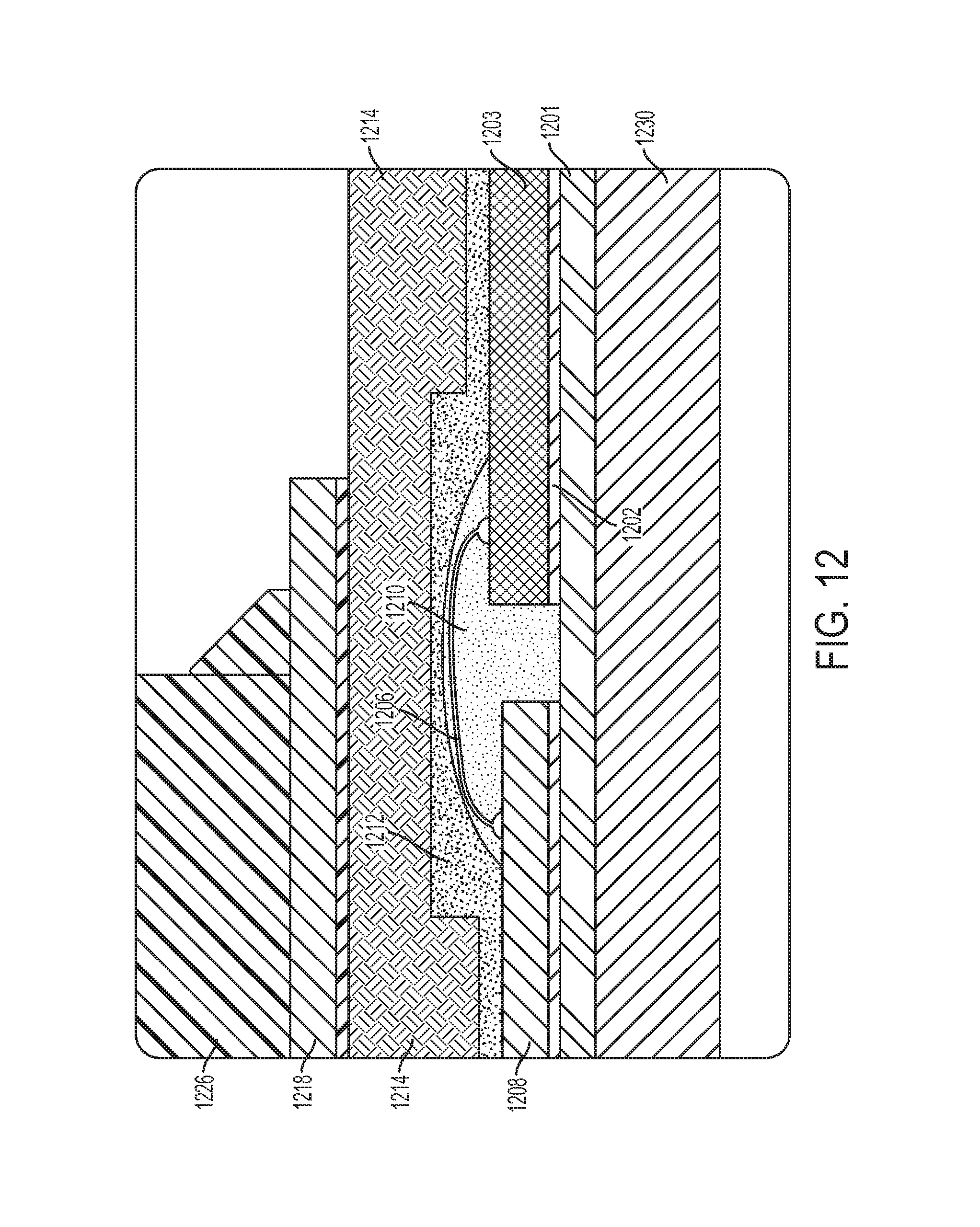
FIG. 112 illustrates another embodiment of an electronic button, with a stacked die configuration. It should be appreciated that the embodiment shown in FIG. 12 is oriented such that the exterior surface of the button (or other input element) is at the bottom of the figure.
The sensor circuit 1201 is shown bonded to a control circuit 1203 via bond 1202, which may be an adhesive. The sensor circuit 1201 may likewise be bonded to flex circuit 1208 by an adhesive or the like. As also shown, the sensor circuit may be positioned adjacent the button, which may be generally cylindrical in shape (although this shape is not necessary).
Wire bonding 1206 connects the flex circuit 1208 to the control circuit 1203, and the wire bonding 1206 is encapsulated by rigid encapsulant 1210 and secondary compliant encapsulant 1212 to protect the wire bonding 1206. The wire bonding 1206 is seated underneath locally thinned stiffener 1214 (with respect to the orientation shown in, and a second flex circuit 1218 is positioned between stiffener 1214 and switch 1226. A complaint encapsulant may fill at least a portion of the space between the stiffener 1214 and one or more of the flex 1208, encapsulant 1210, and control circuit 1203. The stiffener may be locally thinned to form a cavity or depression in which the wire bond and/or rigid encapsulant may be at least partially located.
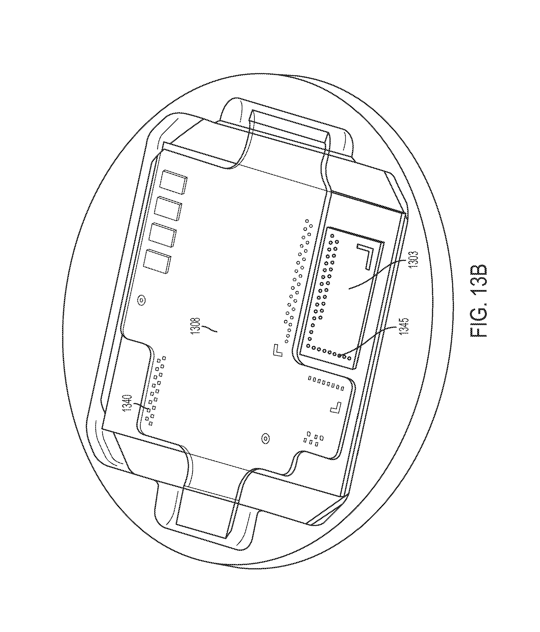
FIG. 13A illustrates a button assembly embodiment, with switch 1326 and trim 1330, and FIG. 13B is a corresponding cross-sectional representation taken along plane P13B in FIG. 13A. FIG. 13B illustrates sensor circuit to flex circuit wire bonds at 1340 and further sensor circuit to control circuit 1303 wire bonds at 1345. The sensor circuit to flex circuit wire bonds 1340 as disclosed in this embodiment carry signals to the underside of the die, where the wires are bonded to the flex circuit 1308 inset from the die perimeter.
The foregoing description has broad application. For example, while examples disclosed herein may focus on a strain gauge type of force sensing circuit, it should be appreciated that the concepts disclosed herein may equally apply to substantially any other type of force sensing circuit with or without appropriate modifications as would be appreciated by one skilled in the art of input members for electronic devices. Moreover, although certain examples have been described with reference to particular figures, it will be understood that other embodiments are also within the scope of this disclosure and the appended claims.
As another example of an alternate embodiment, in some examples a force concentrator may be coupled between the capacitive fingerprint sensor and the strain gauge, and may translate motion of the fingerprint sensor into deflection of the strain gauge, thereby indirectly causing strain. In this manner, strain can be applied in a localized area, which can allow for a very small strain gauge to be used, which may be more accurate and sensitive than a relatively larger strain gauge. This also may allow for thermal separation (e.g., air) between the capacitive fingerprint sensor and the strain gauge.
Accordingly, the discussion of any embodiment is meant only to be exemplary and is not intended to suggest that the scope of the disclosure, including the claims, is limited to these examples.
* * * * *
References
D00000
D00001
D00002
D00003
D00004
D00005
D00006
D00007
D00008
D00009
D00010
D00011
D00012
D00013

D00014
XML
uspto.report is an independent third-party trademark research tool that is not affiliated, endorsed, or sponsored by the United States Patent and Trademark Office (USPTO) or any other governmental organization. The information provided by uspto.report is based on publicly available data at the time of writing and is intended for informational purposes only.
While we strive to provide accurate and up-to-date information, we do not guarantee the accuracy, completeness, reliability, or suitability of the information displayed on this site. The use of this site is at your own risk. Any reliance you place on such information is therefore strictly at your own risk.
All official trademark data, including owner information, should be verified by visiting the official USPTO website at www.uspto.gov. This site is not intended to replace professional legal advice and should not be used as a substitute for consulting with a legal professional who is knowledgeable about trademark law.