Reduction of basal plane dislocations in epitaxial SiC using an in-situ etch process
Myers-Ward , et al.
U.S. patent number 10,256,094 [Application Number 14/204,015] was granted by the patent office on 2019-04-09 for reduction of basal plane dislocations in epitaxial sic using an in-situ etch process. This patent grant is currently assigned to The Government of the United States of America, as represented by the Secretary of the Navy. The grantee listed for this patent is Charles R. Eddy, Jr., David Kurt Gaskill, Nadeemmullah A. Mahadik, Rachael L. Myers-Ward, Robert E. Stahlbush, Virginia D. Wheeler. Invention is credited to Charles R. Eddy, Jr., David Kurt Gaskill, Nadeemmullah A. Mahadik, Rachael L. Myers-Ward, Robert E. Stahlbush, Virginia D. Wheeler.


| United States Patent | 10,256,094 |
| Myers-Ward , et al. | April 9, 2019 |
Reduction of basal plane dislocations in epitaxial SiC using an in-situ etch process
Abstract
A method of: providing an off-axis 4H--SiC substrate, and etching the surface of the substrate with hydrogen or an inert gas.
| Inventors: | Myers-Ward; Rachael L. (Springfield, VA), Gaskill; David Kurt (Alexandria, VA), Eddy, Jr.; Charles R. (Columbia, MD), Stahlbush; Robert E. (Silver Spring, MD), Mahadik; Nadeemmullah A. (Springfield, VA), Wheeler; Virginia D. (Alexandria, VA) | ||||||||||
|---|---|---|---|---|---|---|---|---|---|---|---|
| Applicant: |
|
||||||||||
| Assignee: | The Government of the United States
of America, as represented by the Secretary of the Navy
(Washington, DC) |
||||||||||
| Family ID: | 51061264 | ||||||||||
| Appl. No.: | 14/204,015 | ||||||||||
| Filed: | March 11, 2014 |
Prior Publication Data
| Document Identifier | Publication Date | |
|---|---|---|
| US 20140193965 A1 | Jul 10, 2014 | |
Related U.S. Patent Documents
| Application Number | Filing Date | Patent Number | Issue Date | ||
|---|---|---|---|---|---|
| 12860844 | Aug 20, 2010 | ||||
| 61787903 | Mar 15, 2013 | ||||
| 61235455 | Aug 20, 2009 | ||||
| Current U.S. Class: | 1/1 |
| Current CPC Class: | H01L 21/02529 (20130101); C30B 25/20 (20130101); H01L 21/02378 (20130101); H01L 21/02617 (20130101); C30B 29/36 (20130101); C30B 25/183 (20130101); H01L 21/02433 (20130101); H01L 21/02447 (20130101); H01L 21/02658 (20130101); H01L 21/3065 (20130101) |
| Current International Class: | B44C 1/22 (20060101); H01L 21/02 (20060101); C30B 25/20 (20060101); C30B 29/36 (20060101); C30B 25/18 (20060101); H01L 21/3065 (20060101) |
| Field of Search: | ;216/58,79 ;438/718,931 |
References Cited [Referenced By]
U.S. Patent Documents
| 4912064 | March 1990 | Kong et al. |
| 8652255 | February 2014 | Stahlbush et al. |
| 2001/0011729 | August 2001 | Singh |
| 2006/0011128 | January 2006 | Ellison et al. |
| 2007/0108450 | May 2007 | O'Loughlin et al. |
| 2007/0290211 | December 2007 | Nakayama et al. |
| 2010/0237356 | September 2010 | Haney |
| 2010/0308337 | December 2010 | Sriram |
| 2011/0045281 | February 2011 | Myers-Ward et al. |
| 2012/0018737 | January 2012 | Zhang |
| 2012/0214309 | August 2012 | Itoh |
| 2012/0280254 | November 2012 | Muto et al. |
| 2013/0062628 | March 2013 | Das et al. |
| 2013/0143396 | June 2013 | Sudarshan et al. |
| 2013/0217213 | August 2013 | Aigo et al. |
| 2014/0145214 | May 2014 | Kageshima et al. |
| 2014/0190399 | July 2014 | Myers-Ward et al. |
| WO 2011074453 | Jun 2011 | JP | |||
| WO 2011158528 | Dec 2011 | JP | |||
| 2012067112 | May 2012 | WO | |||
Other References
|
Camara et al.; Solid-State Electronics 46, 2002, pp. 1959-1963, "Study of the reactive ion etching of 6H-SiC and 4H-SiC in SF6/Ar plasma by optical emission spectroscopy and laser interferometry". cited by examiner . Sagar et al. "Morphology and effects of hydrogen etching of porous SiC", Journal of Applied Physics, vol. 92, No. 7, pp. 4070-4074, 2002), herein after refer as Sagar. cited by examiner . Gaskill et al., "Managing Basal Plane Dislocations in SiC: Perspectives and Prospects" ECS 2012 (Oct. 2012). cited by applicant . Myers-Ward et al., Spontaneous Conversion of Basal Plane Dislocations in 4H-SiC Epitaxial Layers ISCSRM 2011 (Sep. 12, 2011). cited by applicant . Myers-Ward et al., "Putting an End to BPDs Starts with Hydrogen Etching" ICSCRM 2103 (Oct. 2013). cited by applicant . Myers-Ward et al., "BPD Conversion in a Thin SiC Buffer Layer" TMS2013 (Mar. 6, 2013). cited by applicant . Myers-Ward et al., "Conversion of BPDs in a Thin SiC Buffer Layer" 2012 Spring Materials Research Society Conference (Apr. 10, 2012). cited by applicant . Myers-Ward et al., "Managing Basal Plane Dislocations in SiC: Perspective and Prospects" ECS Transactions, 50 (3) 103-108 (Oct. 2012). cited by applicant . Stahlbush et al., "Whole-Wafer Mapping of Dislocations in 4H-SiC Epitaxy" Materials Science Forum vols. 556-557 (2007) pp. 295-298. cited by applicant . Stahlbush et al., "Mechanisms of Stacking Fault Growth in SiC PiN Diodes" Mat. Res. Soc. Symp. Proc. vol. 815, J6.4.1 (2004). cited by applicant . Tsuchida et al., "Investigation of Basal Plane Dislocations in the 4H-SiC Epilayers Grown on {0001} Substrates" Materials Science Forum vols. 483-485 (2005) pp. 97-100. cited by applicant . Zhang et al., "Mechanism of eliminating basal plane dislocations in SiC thin films by epitaxy on an etched substrate" Appl. Phys. Lett. 89, 081910 (2006). cited by applicant . Search Report and Written Opinion in PCT/2014/023148 (dated Aug. 27, 2014). cited by applicant . Office Action in U.S. Appl. No. 14/204,045 (dated Sep. 22, 2014). cited by applicant . Office Action in U.S. Appl. No. 14/204,045 (dated Mar. 6, 2015). cited by applicant . Examiner's Answer in U.S. Appl. No. 14/204,045 (dated Jan. 8, 2016). cited by applicant. |
Primary Examiner: Tran; Binh X
Attorney, Agent or Firm: US Naval Research Laboratory Grunkemeyer; Joseph T.
Parent Case Text
This application claims the benefit of U.S. Provisional Application No. 61/787,903, filed on Mar. 15, 2013. This application is a continuation-in-part application of pending U.S. patent application Ser. No. 12/860,844, filed on Aug. 20, 2010, which claims the benefit of U.S. Provisional Application No. 61/235,455, filed on Aug. 20, 2009. These applications are incorporated herein by reference.
Claims
What is claimed is:
1. A method comprising: providing an off-axis 4H--SiC substrate; and etching the surface of the substrate with an inert gas.
2. The method of claim 1, wherein the substrate is a 4.degree. off-axis 4H--SIC substrate.
3. The method of claim 1, wherein the inert gas is argon.
4. The method of claim 1, further comprising: growing a doped buffer layer directly on the substrate after the etching.
5. The method of claim 4, further comprising: growing an epitaxial silicon carbide layer on the doped buffer layer.
6. A method comprising: providing a 4.degree. off-axis 4H--SiC substrate; etching the surface of the substrate with hydrogen; and growing a doped buffer layer directly on the substrate after the etching.
7. The method of claim 6, wherein the doped buffer layer is doped with N.sup.+.
8. The method of claim 6, wherein the doped buffer layer is about 6.5-8 .mu.m thick.
9. The method of claim 6, further comprising: growing an epitaxial silicon carbide layer on the doped buffer layer.
10. The method of claim 6, wherein the etching is performed at 40-70mbar of the hydrogen.
11. The method of claim 6, wherein the etching is performed for 5-90 minutes.
12. The method of claim 6, wherein the etching is performed at 1620-1665.degree. C.
Description
TECHNICAL FIELD
The present disclosure is generally related to SiC epitaxial growth.
DESCRIPTION OF RELATED ART
Since the ABB (Asea Brown Boveri, Inc.--Sweden) power company disclosed the forward voltage, V.sub.f, drift problem that degraded their PiN diodes (Lendenmann et al., Mater. Sci. Forum, 353-356 (2001) 727-730), it has been well established that the V.sub.f drift problem is due to stacking faults that originate from basal plane dislocations (BPDs) and that the only way to overcome this problem is to reduce the BPD density in low-doped portions of the epitaxial layer that forms the active region of SiC power devices. The major source of BPDs in the epitaxy is from BPDs in the SiC substrate. At the start of epitaxial growth, 70-90% of the substrate BPDs are converted to threading edge dislocations (TEDs) and the resulting BPD density in the epitaxy is typically in the 100-1000 cm.sup.-2 range; a further reduction to<1 cm.sup.-2 is required for device production, based on the area of desired devices. For devices requiring higher power, the problem of BPDs becomes exacerbated since these devices require larger areas and hence further reduction of BPDs is essential.
Several techniques have been developed to decrease BPD density in the epitaxy. One technique uses a growth interrupt to turn the BPDs into TEDs (VanMil et al., PCSI (2008); U.S. Pat. No. 8,652,255). Two other techniques alter the wafer surface before epitaxial growth. The first is a surface patterning process that was originally developed and patented by ABB and later used by Cree (Sumakeris et al., Mater. Sci. Forum, 527-529 (2006) 141-146). The second is a process that involves KOH etching, epitaxial growth, and repolishing. It was developed and patented by Cree. Cree has tested both processes and found the KOH etching method to be more effective (Sumakeris Id.). Another technique is to grow the epitaxial layers on wafers with an offcut angle lower than the standard 8.degree. angle used for 4H--SiC (Chen et al., J. Appl. Phys. 98 (2005) 114907). The tradeoff is that lowering the offcut angle tends to introduce 3C inclusions that degrade device performance (Kojima et al., J. Cryst. Growth, 269 (2004) 367-376). Growth on 4.degree. offcut substrates has also been demonstrated to convert BPDs to TEDs throughout the epitaxial growth process (U.S. Patent Appl. Pub. No. 2011/0045281).
BRIEF SUMMARY
Disclosed herein is a method comprising: providing an off-axis 4H--SiC substrate; and etching the surface of the substrate with hydrogen or an inert gas.
BRIEF DESCRIPTION OF THE DRAWINGS
A more complete appreciation of the invention will be readily obtained by reference to the following Description of the Example Embodiments and the accompanying drawings.
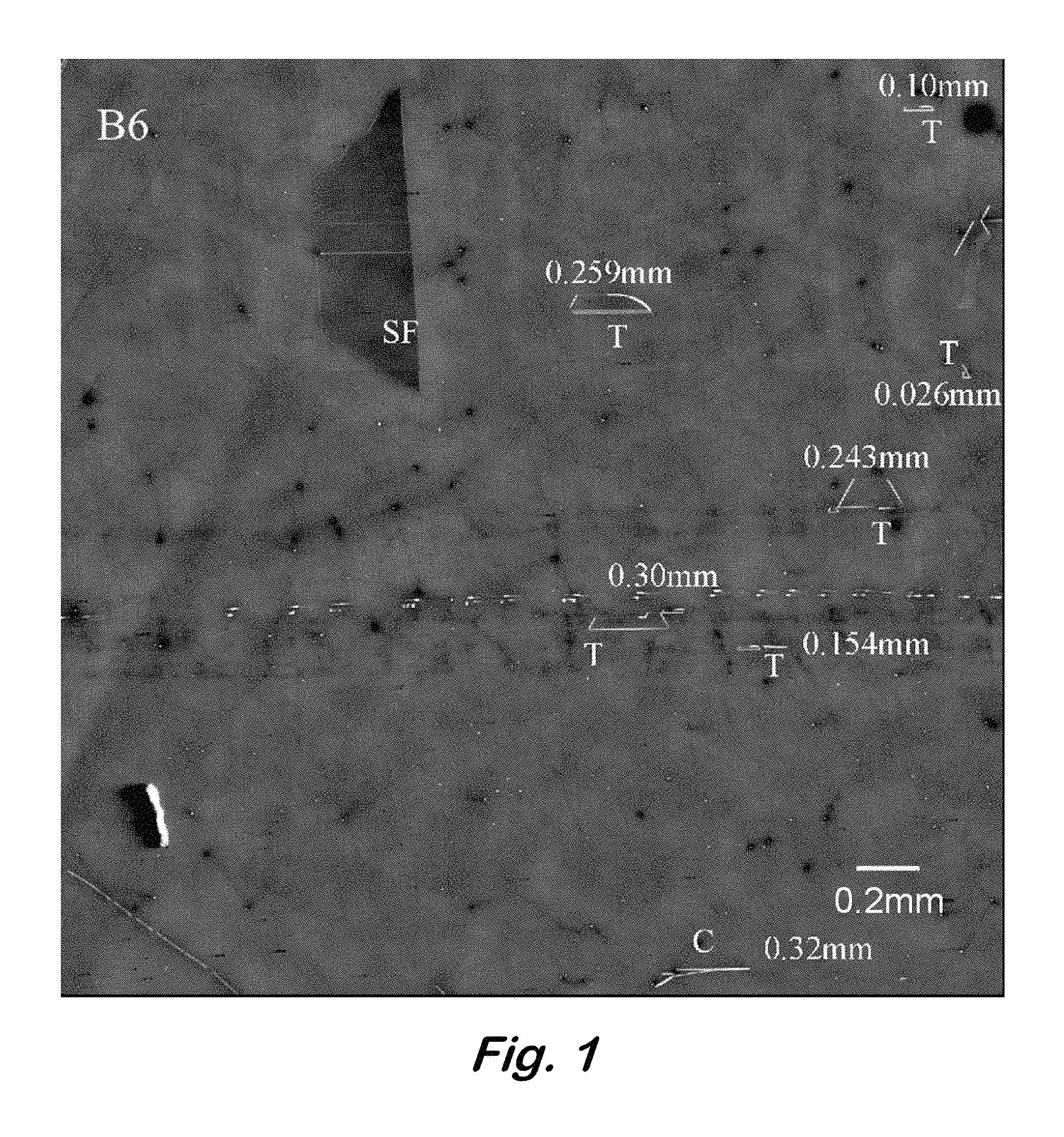
FIG. 1 shows a UVPL image of UID film showing various lengths of BPDs; C=continued, T=turned (converted to TED). Image sizes are 3 mm.times.3 mm.
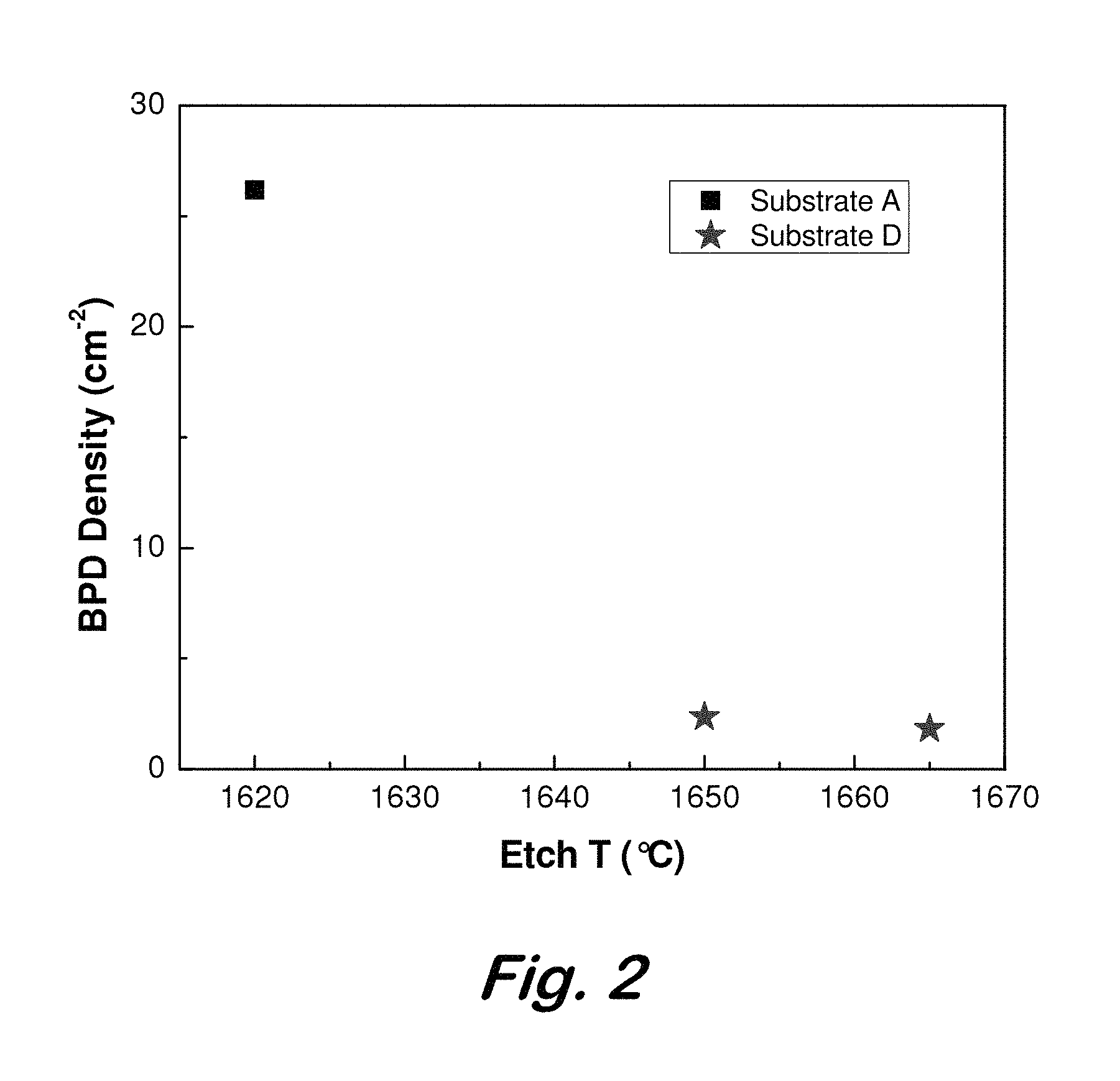
FIG. 2 shows BPD density as a function of etch temperature
FIG. 3 shows BPD density as a function of etch pressure.
DETAILED DESCRIPTION OF EXAMPLE EMBODIMENTS
In the following description, for purposes of explanation and not limitation, specific details are set forth in order to provide a thorough understanding of the present disclosure. However, it will be apparent to one skilled in the art that the present subject matter may be practiced in other embodiments that depart from these specific details. In other instances, detailed descriptions of well-known methods and devices are omitted so as to not obscure the present disclosure with unnecessary detail.
The method may be employed in a wide range of bipolar SiC device technologies enabling them to achieve higher performance levels. Such devices range from power diodes and switches to rf transistors and UV photodetectors. The purpose of using a hydrogen etch prior to a SiC epitaxial growth process on 4.degree. off-axis substrates is to reduce BPDs within the active regions of SiC devices leading to improved device performance and reliability. The etch process is used to increase the conversion of basal plane dislocations into threading edge dislocations and have the converted BPDs in a thin highly doped buffer layer. It has been demonstrated that BPDs cause increasing forward voltage drift in bipolar SiC devices and there are also reports in the literature that they can degrade majority carrier mobility and increase reverse-biased leakage (Agarwal et al., Elec. Dev. Lett., 28 (2007) 587). BPD reduction processes that utilize epitaxial growth are all based on the principle of converting BPDs into TEDs, which have negligible adverse effects on the SiC devices.
In the disclosed method an off-axis 4H--SiC substrate is used. The off angle may be, but is not limited to, 4.degree.. The surface of the substrate is then etched with hydrogen or an inert gas, such as argon. The etching takes place before any epitaxial growth. Suitable etching conditions include, but are not limited to, 1620-1665.degree. C., 40-130 mbar of the etching gas, and 5-90 minutes of etching.
After the etching, a doped buffer layer may be grown on the substrate. The buffer layer may be doped with, for example, N.sup.+, and may be about 6.5-8 .mu.m thick. An epitaxial silicon carbide layer may then be grown on the buffer layer.
To determine the efficacy of the method, investigations were carried out using the following approach. To determine where the BPD converts to a TED in the epitaxial layer, 3 key ingredients are required: (1) the length of the BPD photoluminescence image taken in the plan view, (2) the orientation of the surface with respect to the basal plane of the sample (also known as the off-cut angle), and (3) the thickness of the epitaxial layer. For the first, ultra-violet photoluminescence images (UVPL images) were obtained using well-established techniques previously published (Stahlbush et al., Mater. Sci. Forum 556-55 (2007) 295). X-ray diffraction (XRD) rocking curve maps of the symmetric (0008) reflection were analyzed to determine the off-cut angle of the substrates. The manufacturer labels the wafers off-cut on the substrate wafer carrier, however, this is not always the exact off-cut. Additionally, this angle is not typically constant across the wafers (100, 75, or 50 mm) due to lattice curvature associated with the manufacturing process of the wafers. With that in mind, the precise, spatially-resolved off-cut angle determined from the XRD rocking curve measurement maps was used for each sample in the NRL research investigation which typically consisted of a quartered 75 or 100 mm wafer to determine what a full length BPD would be if it extended through to the epi surface. Finally, the third key ingredient was measuring the precise thickness of the epitaxial films, evaluated using Fourier transform infrared measurements. With (1), (2), and (3) and using standard geometry, the plan view length of a BPD could be converted to a z-axis distance that the BPD covered from the beginning of growth to where it ends. If the distance is found to be less than that of the epitaxial layer thickness, then the BPD is known to have converted in to a threading edge dislocation (TED). If the distance is equal to that of the epitaxial layer thickness, then the BPD did not convert to a TED in the epitaxial layer.
The injected carrier lifetimes of some of the samples were evaluated using room temperature time-resolved photoluminescence, were they varied from 1000 to 1800 ns. The surface roughness of a film may also influence the device properties as well as make processing difficult; therefore, AFM analysis was also performed to determine surface roughness. Samples investigated resulted in similar surface morphology, with a surface roughness of .about.3.0 nm RMS. Carrier concentrations were also measured on several of the samples using Hg probe CV measurements, where the net carrier concentration was.ltoreq.2.5.times.10.sup.14 cm.sup.-3.
Table 1 summarizes the results of several experiments. The films were either unintentionally (UID) or intentionally doped (ID) net carrier concentration<4.times.10.sup.14 cm.sup.-3 using a nitrogen source gas. All films were grown at a temperature of .about.1600.degree. C., pressure of 100 mbar and gas phase carbon-to-silicon (C/Si) ratio of 1.55 using an Aixtron VP508 reactor. The temperature was ramped from room temperature to a temperature of 1400.degree. C. in a hydrogen atmosphere. At this time, either the pressure was maintained at 100 mbar, or it was adjusted to a value between 40 mbar and 130 mbar. The temperature was then ramped to the etch temperature (between 1620.degree. C. and 1665.degree. C.). Once the temperature was reached, an etch step took place prior to the growth of a highly doped N.sup.+ buffer layer. The thickness of the buffer layer was .about.6.5 .mu.m and was incorporated prior to the low doped epilayer, with the exception of one buffer layer thickness being -8 .mu.m. All samples were .about.20 .mu.m thick (not including buffer layers, where applicable) and were grown at .about.10 .mu.m/h, except sample C1110829, which was 13 .mu.m thick and no buffer layer was grown. Experiments were conducted where only an etch took place to evaluate the surface of the substrate and determine the etch rate. It was found that the etch rate varied time and temperature and is shown in Table 2. The conversion process, i.e. instituting the in-situ etch, prior to growth was carried out for an epitaxial layer. UVPL images of this sample were analyzed and showed after a 50 min etch at 1620.degree. C., 70 mbar and an 8.1 .mu.m N.sup.+ buffer layer, there were 144 BPDs extending out of the buffer into the unintentionally doped 20 micron layer.
TABLE-US-00001 TABLE 1 Tabulation of basal plane dislocations conversion efficiency for epitaxial growth on 4.degree. off-axis substrates Etch Time Etch T Etch P BL Thickness Epi Thickness Sample ID Substrate (min) (.degree. C.) (mbar) (.mu.m) (.mu.m) BPD BPD/cm.sup.2 C1110820 BD1787-44-iv 50 1620 70 8.13 19.57 144 26.2 C1110829 BD1796-51-iii 50 1620 70 0 12.81 218 39.6 C1110830 50 1620 70 C1110927 BD1796-51-iv 50 1650 70 6.78 19.41 13 2.4 C2111017 BD1796-52-iv 50 1665 70 6.5 18.5 10 1.8 C2111019 BD1796-52-ii 50 1665 70 C2111021A BD1796-52-iii 50 1665 70 C2111025A BD1787-40-i 50 1665 70 C2111109 BD1787-40-ii 90 1665 70 6.6 18.9 65 11.8 C2120320 BD1787-40-iii 90 1665 40 6.7 19.2 145 26.4 C2111229 GW0608-10-iii 5 1620 100 C2120406A BD1787-40-iv 90 1665 100 73 13.3 C2120406B DA1090-52-ii 90 1665 100 402 73 C2120504 DA1090-53-iii 90 1665 130 286 52 C2120709 DA1090-53-i 50 1650 70 C2130204 GT0011 50 1630 40 G2130206 GT0011 50 1630 70 6.5 19.7 61 5.3 C2130207 GT0011 50 1630 100 6.5 19.7 71 6.1 C2130208 GT0011 50 1630 130 6.5 19.7 203 17.5
TABLE-US-00002 TABLE 2 Amount of SiC removed during the hydrogen etch step Etch Time Etch Temperature Etch Pressure Material (min) (.degree. C.) (mbar) removed (.mu.m) 5 1620 70 0.45 50 1620 70 1.34 50 1665 70 3.13
The full length of continuous BPDs were determined using XRD rocking curve maps and film thicknesses found by using FTIR measurements. The spatially-resolved XRD maps were used to determine the accurate off-cut angle of each quarter wafer prior to growth. After growth, incorporating the spatially-resolved thickness measurements combined with the off-cut angle, the expected full length BPD was determined. The BPD lengths were then measured from the UVPL images using the software program, "ImageJ" by measuring the horizontal length from left to right of the BPD, see FIG. 1. The lengths of the BPDs were then tallied and the conversion efficiency (number of BPDs that have converted to threading edge dislocations) was based on comparing the actual length of each BPD to the full length BPD. With the variation of lattice curvature across a quarter wafer, it was essential to obtain the precise measurement of the off-cut angle across the substrate, combined with the accurate film thickness to correctly identify the actual BPD full length and correctly reveal the trend of BPDs converting to TEDs within the epilayer. Plots of the BPD density as a function of etch temperature and pressure is shown in FIGS. 2 and 3. The temperature influences the conversion at elevated temperatures>1620.degree. C. The pressure influences the conversion and is clearly seen in FIG. 3. There is an optimized pressure of 70-100 mbar for higher conversion of BPDs.
This process for determining conversion efficiency is more accurate than others used in the field. Typically, the BPD density is found using KOH etching, which creates etch pits on the surface of the wafer, and these pits are counted. A low BPD density that has been published in the literature is 2.6 cm.sup.2 using KOH etching (Chen et al., J. Appl. Phys. 98 (2005) 114907). If the above samples had been investigated using KOH etching, the BPD density would be zero for the majority of the samples. However, from the UVPL images, it can be seen that the BPDs are turning throughout the film on 4.degree. off-cut substrates. By using the KOH etching approach, the number of BPDs in the active region may be much higher than what is at the surface of the epilayer. This means that conclusions given by prior investigations using the KOH etching approach are not accurate and have only limited value in developing methods for BPD reduction. By employing the UVPL technique, the total number of BPD in the entire active region is determined. Therefore, the result of 10 BPDs in the epilayer shown in Table 1 is significant.
A phenomenon called "step bunching" may influence the conversion of BPDs into TEDs during the growth of epitaxial films on 4 degree off-cut substrates. The formation of multi-unit cell high surface steps may create a potential barrier to continued basal plane dislocation propagation out of the substrate and that an energy balance may be created that makes it more favorable for the BPD to convert to a TED than to continue propagating. Ha et al., J. Cryst. Growth 244 (2002) 257-266 describes that the image force is the driving force of BPD conversion to TED, speculates that "when the critical distance is small in the range of several bilayers or several nanometers, a dislocation can see two surfaces of the step structure, the terrace and the step, which are different from the average off-axis surface. In this case, the conversion will depend on the step structure". It is also reported that one "can expect that a basal plane dislocation will be attracted by the surface of the last one or two macro-steps and, that the `step facet mechanism` . . . will be governing the dislocation conversion". Therefore, a processing window that is a function of growth rate, doping, off-cut angle, C/Si ratio, temperature and pressure determine the optimal condition for conversion rate. During the etching, etch pits may be formed on the surface and the BPDs may be converted to TEDs at the pit.
A hydrogen etch process prior to the epitaxial growth process on 4.degree. off-axis enables the conversion of BPDs into TEDs--making it extremely manufacturable. It has been found experimentally that the BPDs convert to TEDs after the hydrogen etch process, followed by a thin, .about.6.5 .mu.m highly doped N.sup.+ buffer layer and the lowest density of BPDs was 1.8 cm .sup.-2. The process is easy to implement into a manufacturable process. Growing the N.sup.+ buffer layer will enable one to bury the BPDs in a thinner buffer layer, producing a BPD free active region. This is the optimal situation as it will permit the economic realization of a wide range of high voltage, bipolar devices.
Other techniques that have been used to convert BPDs to TEDs during epitaxial growth are the three mentioned in the Background Art above. The first is patterning the surface of the SiC wafer before the epitaxial growth, which increases the BPD-to-TED conversion at the beginning of the growth. It has the tendency to increase other detrimental extended defects such as ingrown faults. The second technique is to etch the wafer in molten KOH before epitaxial growth. This creates pits at each of the dislocations including the BPDs, and this technique also increases the BPD-to-TED conversion at the beginning of the growth. However, the top of the growth surface remains pitted creating challenges for device manufacturing. An initial layer is grown and the wafer is polished to restore a smooth surface. It should be noted that this latter technique involves handling and wafers polishing which significantly adds to the overall cost of the final product. The third technique from Chen and Capano is to use wafers with a smaller offcut angle than the standard 8.degree. angle. As with the previous techniques, it increases the BPD-to-TED conversion at the beginning of the growth. The tradeoff is that lowering the offcut angle results in step bunching which is more difficult to control. Further, such growths can lead to SiC polytype inclusions that are also device killers.
The reduction of BPDs relies on the conversion of BPDs to threading edge dislocations (TEDs) during the epitaxial growth process and/or the substrate/epilayer interface due to the etch process prior to growth as the surface is modified during the etch to improve the conversion of BPDs. The growth process includes a step that consists of ramping the temperature from room temperature to growth temperature, during which time hydrogen is flowing. The etching takes place for a certain amount of time, after which the growth process takes place. There are many parameters which may be varied during the ramp process and the growth process which may influence the BPD conversion efficiency and rate.
The following lists the specific process parameters which may be manipulated to result in optimal BPD conversion. 1) Propane flow rate during ramp to etch temperature and etch process--modifying the propane flow rate during ramp has been shown experimentally to influence the number of initial BPDs at the substrate/epilayer or buffer layer/epilayer interface (Myers-Ward et al., Mat. Sci. Forum 615-617 (2009) 105108) 2) Silane flow rate during ramp to etch temperature and during etch process--incorporate a silane flow during these steps 3) Temperature at which point the pressure is adjusted for the etch process--vary the temperature at which point the pressure for etch is modified to influence the BPD conversion 4) Temperature of etch step--vary the temperature during etch to influence the effect of step bunching and/or etch pits on the surface since this may be the key factor in converting BPDs into TEDs 5) Incorporating a halogen during the etch process before growth--Use the halogen to assist in etching the surface to influence the conversion of BPDs 6) Using an inert gas instead of hydrogen--Use Ar instead of hydrogen during the etch to control the surface of the material prior to growth, or a mixture of inert gas plus hydrogen gas 7) Vary the amount of hydrogen flow during the etch process--varying the flow will assist in modifying the surface to achieve the desired surface for the highest conversion rate 8) Etch Time--vary the etch time to achieve highest conversion rate 9) Pressure during etch--vary etch pressure to achieve highest conversion rate 10) Initiation of growth--Initiate the growth differently after the etch process
Obviously, many modifications and variations are possible in light of the above teachings. It is therefore to be understood that the claimed subject matter may be practiced otherwise than as specifically described. Any reference to claim elements in the singular, e.g., using the articles "a," "an," "the," or "said" is not construed as limiting the element to the singular.
* * * * *
D00000
D00001
D00002
D00003
XML
uspto.report is an independent third-party trademark research tool that is not affiliated, endorsed, or sponsored by the United States Patent and Trademark Office (USPTO) or any other governmental organization. The information provided by uspto.report is based on publicly available data at the time of writing and is intended for informational purposes only.
While we strive to provide accurate and up-to-date information, we do not guarantee the accuracy, completeness, reliability, or suitability of the information displayed on this site. The use of this site is at your own risk. Any reliance you place on such information is therefore strictly at your own risk.
All official trademark data, including owner information, should be verified by visiting the official USPTO website at www.uspto.gov. This site is not intended to replace professional legal advice and should not be used as a substitute for consulting with a legal professional who is knowledgeable about trademark law.