Systems and methods for tiling free space optical transmissions
Shatz , et al.
U.S. patent number 10,236,986 [Application Number 15/863,817] was granted by the patent office on 2019-03-19 for systems and methods for tiling free space optical transmissions. This patent grant is currently assigned to ARON SUREFIRE, LLC. The grantee listed for this patent is ARON SUREFIRE, LLC. Invention is credited to John C. Bortz, Narkis E. Shatz.


View All Diagrams
| United States Patent | 10,236,986 |
| Shatz , et al. | March 19, 2019 |
Systems and methods for tiling free space optical transmissions
Abstract
Systems and methods for optical narrowcasting are provided for transmitting various types of content. Optical narrowcasting content indicative of the presence of additional information along with identifying information may be transmitted. The additional information (which may include meaningful amounts of advertising information, media, or any other content) may also be transmitted as optical narrowcasting content. Elements of an optical narrowcasting system may include optical transmitters and optical receivers which can be configured to be operative at distances ranging from, e.g., 400 meters to 1200 meters. At such far-field distances, light beams emitted from the optical transmitters can be combined in a tiled fashion to create energy efficient and directable optical transmissions.
| Inventors: | Shatz; Narkis E. (La Jolla, CA), Bortz; John C. (Spokane, WA) | ||||||||||
|---|---|---|---|---|---|---|---|---|---|---|---|
| Applicant: |
|
||||||||||
| Assignee: | ARON SUREFIRE, LLC (Fountain
Valley, CA) |
||||||||||
| Family ID: | 65721790 | ||||||||||
| Appl. No.: | 15/863,817 | ||||||||||
| Filed: | January 5, 2018 |
| Current U.S. Class: | 1/1 |
| Current CPC Class: | H04B 10/1121 (20130101); H04B 10/116 (20130101); H04B 10/516 (20130101); H04B 10/502 (20130101); H04B 10/50 (20130101) |
| Current International Class: | H04B 10/00 (20130101); H04B 10/116 (20130101); H04B 10/50 (20130101) |
| Field of Search: | ;398/118,119,122,124,125,126,127,128,129,130,131,135,136,115,158,159,120,123,172 |
References Cited [Referenced By]
U.S. Patent Documents
| 3761184 | September 1973 | McLaughlin |
| 3987297 | October 1976 | Brienza |
| 4114592 | September 1978 | Winston |
| 4600843 | July 1986 | Kizu |
| 5005040 | April 1991 | Norita |
| 5029195 | July 1991 | Danos |
| 5229984 | July 1993 | Konno |
| 5359446 | October 1994 | Johnson |
| 5475253 | December 1995 | Look |
| 5475523 | December 1995 | Shinada |
| 5566022 | October 1996 | Segev |
| 5596452 | January 1997 | Yamakawa |
| 5598281 | January 1997 | Zimmerman |
| 5604630 | February 1997 | Palmer |
| 5610753 | March 1997 | Kessler |
| 5717510 | February 1998 | Ishikawa |
| 5777768 | July 1998 | Korevaar |
| 5778256 | July 1998 | Darbee |
| 5835199 | November 1998 | Phillips |
| 5894195 | April 1999 | McDermott |
| 5896217 | April 1999 | Ishikawa |
| 5944281 | August 1999 | Pittman |
| 5947587 | September 1999 | Keuper |
| 5999294 | December 1999 | Petsko |
| 6019493 | February 2000 | Kuo |
| 6065880 | May 2000 | Thompson |
| 6104513 | August 2000 | Bloom |
| 6122084 | September 2000 | Britz |
| 6229631 | May 2001 | Sato |
| 6260763 | July 2001 | Svetal |
| 6292283 | September 2001 | Grandbois |
| 6324013 | November 2001 | Nakai |
| 6381055 | April 2002 | Javitt |
| 6410942 | June 2002 | Thibeault |
| 6501581 | December 2002 | Snyder |
| 6504632 | January 2003 | Watanabe |
| 6529329 | March 2003 | Dang |
| 6559993 | May 2003 | Doucet |
| 6560038 | May 2003 | Parkyn |
| 6568627 | May 2003 | Jones |
| 6594090 | July 2003 | Kruschwitz |
| 6643068 | November 2003 | Mandella |
| 6653551 | November 2003 | Chen |
| 6657790 | December 2003 | Kim |
| 6822634 | November 2004 | Kemp |
| 6829439 | December 2004 | Sidorovich |
| 6859326 | February 2005 | Sales |
| 6868237 | March 2005 | Willebrand |
| 6910780 | June 2005 | Vail |
| 7019676 | March 2006 | Ikoma |
| 7021797 | April 2006 | Min ano |
| 7035546 | April 2006 | Keller |
| 7058316 | June 2006 | Vilnrotter |
| 7079774 | July 2006 | Sidorovich |
| 7099649 | August 2006 | Patterson |
| 7106973 | September 2006 | Kube |
| 7116661 | October 2006 | Patton |
| 7120363 | October 2006 | Andreu-von Euw |
| 7130505 | October 2006 | Shen |
| 7170600 | January 2007 | Nishii |
| 7186004 | March 2007 | Powell |
| 7203424 | April 2007 | Alwan |
| 7221910 | May 2007 | Ishii |
| 7223315 | May 2007 | Chen |
| 7245798 | July 2007 | Graves |
| 7308194 | December 2007 | Iizuka |
| 7319822 | January 2008 | Lo |
| 7324271 | January 2008 | Winterot |
| 7375804 | May 2008 | Liebman |
| 7382103 | June 2008 | Shirazee |
| 7390129 | June 2008 | Yonekubo |
| 7401948 | July 2008 | Chinniah |
| 7415212 | August 2008 | Matsushita |
| 7450857 | November 2008 | Dress |
| 7480101 | January 2009 | Lubart |
| 7493046 | February 2009 | Kyoto |
| 7495837 | February 2009 | Smith |
| 7508588 | March 2009 | Nakajima |
| 7534986 | May 2009 | Nakaso |
| 7538879 | May 2009 | Power |
| 7554076 | June 2009 | Wang |
| 7565082 | July 2009 | Yazaki |
| 7583901 | September 2009 | Nakagawa |
| 7587141 | September 2009 | Fisher |
| 7630648 | December 2009 | Dress |
| 7639948 | December 2009 | Gilbert |
| 7657182 | February 2010 | Hase |
| 7663501 | February 2010 | Hyun |
| 7699229 | April 2010 | Bennett |
| 7715723 | May 2010 | Kagawa |
| 7734181 | June 2010 | Bahar |
| 7800541 | September 2010 | Moshfeghi |
| 7806547 | October 2010 | Benitez |
| 7810963 | October 2010 | Peck |
| 7883226 | February 2011 | Li |
| 7884931 | February 2011 | Achal |
| 7885547 | February 2011 | Nakaso |
| 7889998 | February 2011 | Son |
| 7907345 | March 2011 | Paulussen |
| 7918583 | April 2011 | Chakmakjian |
| 7953326 | May 2011 | Farr |
| 7970279 | June 2011 | Dress |
| 8000018 | August 2011 | Benitez et al. |
| 8029167 | October 2011 | Ikeda |
| 8031414 | October 2011 | Liu |
| 8032016 | October 2011 | Duling |
| 8036244 | October 2011 | Naoe |
| 8075147 | December 2011 | Chaves |
| 8081876 | December 2011 | Dress |
| 8103167 | January 2012 | Tidhar |
| 8148663 | April 2012 | Adams |
| 8152327 | April 2012 | Brands |
| 8204383 | June 2012 | Shin |
| 8246210 | August 2012 | Angelini |
| 8269971 | September 2012 | Marsh |
| 8301027 | October 2012 | Shaw |
| 8304733 | November 2012 | Alameh |
| 8406427 | March 2013 | Chand |
| 8417058 | April 2013 | Tardif |
| 8422119 | April 2013 | Keaton |
| 8452182 | May 2013 | Davidson |
| 8488244 | July 2013 | Li |
| 8526403 | September 2013 | Nadji |
| 8582973 | November 2013 | Takahashi |
| 8593647 | November 2013 | Charny |
| 8611754 | December 2013 | Templ |
| 8639106 | January 2014 | Gleason |
| 8687965 | April 2014 | Pederson |
| 8706815 | April 2014 | Redmond |
| 8780446 | July 2014 | Lee |
| 8805192 | August 2014 | Eide |
| 8829392 | September 2014 | Adams |
| 8831427 | September 2014 | Grubor |
| 8848059 | September 2014 | Tiscareno |
| 8908074 | December 2014 | Oshima |
| 8922666 | December 2014 | Oshima |
| 8923701 | December 2014 | D'Errico |
| 8948601 | February 2015 | Shar |
| 8965214 | February 2015 | Weckwerth |
| 8965215 | February 2015 | Na |
| 9022601 | May 2015 | Lu |
| 9066084 | June 2015 | Zalevsky |
| 9066087 | June 2015 | Shpunt |
| 9118420 | August 2015 | Kwon |
| 9134538 | September 2015 | Augst |
| 9143232 | September 2015 | Bhide |
| 9146103 | September 2015 | Rousseau |
| 9166683 | October 2015 | Jovicic |
| 9167138 | October 2015 | Shpunt |
| 9203524 | December 2015 | Simpson |
| 9210376 | December 2015 | Yu |
| 9215032 | December 2015 | Zhang |
| 9225427 | December 2015 | Jung |
| 9250355 | February 2016 | Deng |
| 9252875 | February 2016 | Bae |
| 9264136 | February 2016 | Vaananen |
| 9300398 | March 2016 | Chaffee |
| 9317747 | April 2016 | Jovicic |
| 9350448 | May 2016 | Byers |
| 9360185 | June 2016 | Demuynck |
| 9360554 | June 2016 | Retterath |
| 9386666 | July 2016 | Economy |
| 9401121 | July 2016 | Chen |
| 9420264 | August 2016 | Gilliland |
| 9438337 | September 2016 | Byers |
| 9453976 | September 2016 | Qian |
| 9509402 | November 2016 | Ryan |
| 9520939 | December 2016 | Jovicic |
| 9551914 | January 2017 | Pellman |
| 9601670 | March 2017 | Bhat |
| 9654222 | May 2017 | Shatz |
| 9657918 | May 2017 | Wilcox |
| 9742520 | August 2017 | Way |
| 9755740 | September 2017 | Shatz |
| 10009108 | June 2018 | Elahmadi |
| 2002/0089726 | July 2002 | He |
| 2002/0109884 | August 2002 | Presley |
| 2002/0118344 | August 2002 | Fischer |
| 2002/0149822 | October 2002 | Stroud |
| 2002/0163699 | November 2002 | Kavehrad |
| 2003/0026002 | February 2003 | Lopez-Hernandez |
| 2003/0076034 | April 2003 | Marshall |
| 2003/0090765 | May 2003 | Neff |
| 2003/0151818 | August 2003 | Wagner |
| 2004/0135935 | July 2004 | Glaeser |
| 2004/0141753 | July 2004 | Andreu-von Euw |
| 2004/0156640 | August 2004 | Dress |
| 2004/0161246 | August 2004 | Matsushita |
| 2004/0208596 | October 2004 | Bringans |
| 2004/0208602 | October 2004 | Plante |
| 2004/0252520 | December 2004 | Martineau |
| 2004/0258414 | December 2004 | Lee |
| 2004/0263500 | December 2004 | Sakata |
| 2005/0036789 | February 2005 | Bjorndahl |
| 2005/0169643 | August 2005 | Franklin |
| 2005/0226636 | October 2005 | Hiramatsu |
| 2006/0018661 | January 2006 | Green |
| 2006/0076473 | April 2006 | Wilcken |
| 2006/0153498 | July 2006 | Shen |
| 2006/0222041 | October 2006 | Moriwaka |
| 2006/0285852 | December 2006 | Xi |
| 2007/0070060 | March 2007 | Kagawa |
| 2007/0070834 | March 2007 | Masui |
| 2007/0127926 | June 2007 | Marioni |
| 2007/0133097 | June 2007 | Lubart |
| 2007/0147843 | June 2007 | Fujiwara |
| 2007/0206952 | September 2007 | Hase |
| 2007/0253716 | November 2007 | Nakaso |
| 2007/0263298 | November 2007 | El-Ghoroury |
| 2008/0008471 | January 2008 | Dress |
| 2008/0008472 | January 2008 | Dress |
| 2008/0043466 | February 2008 | Chakmakjian |
| 2008/0074752 | March 2008 | Chaves |
| 2008/0095533 | April 2008 | Lee |
| 2008/0107419 | May 2008 | Won |
| 2008/0123062 | May 2008 | Morikuni |
| 2008/0124083 | May 2008 | Esser et al. |
| 2008/0131134 | June 2008 | Dreischer |
| 2008/0138077 | June 2008 | Stretton |
| 2008/0152353 | June 2008 | De Boer |
| 2008/0170296 | July 2008 | Chaves |
| 2008/0218850 | September 2008 | Power |
| 2008/0240722 | October 2008 | Karaki |
| 2008/0262718 | October 2008 | Farwell |
| 2009/0028564 | January 2009 | Villarruel |
| 2009/0041459 | February 2009 | Dress |
| 2009/0103925 | April 2009 | Alpert |
| 2009/0128921 | May 2009 | Roth |
| 2009/0244716 | October 2009 | Mathai |
| 2010/0003029 | January 2010 | Dress |
| 2010/0091134 | April 2010 | Cooke |
| 2010/0096993 | April 2010 | Ashdown |
| 2010/0097002 | April 2010 | Shatford |
| 2010/0157434 | June 2010 | Lee |
| 2010/0188753 | July 2010 | Paulussen |
| 2010/0257569 | October 2010 | O'Hanlon |
| 2011/0026931 | February 2011 | Koizumi |
| 2011/0157566 | June 2011 | Akiyama |
| 2011/0267823 | November 2011 | Angelini |
| 2011/0270585 | November 2011 | Chen |
| 2012/0060177 | March 2012 | Stinson |
| 2012/0068913 | March 2012 | Bar-Zeev |
| 2012/0098934 | April 2012 | McKiel |
| 2012/0098945 | April 2012 | McKiel |
| 2012/0106200 | May 2012 | Yin |
| 2012/0148189 | June 2012 | Zhang |
| 2012/0287511 | November 2012 | Dross |
| 2013/0004173 | January 2013 | Maricevic |
| 2013/0061259 | March 2013 | Raman |
| 2013/0126713 | May 2013 | Haas |
| 2013/0216063 | August 2013 | Sherman |
| 2013/0236183 | September 2013 | Chao |
| 2013/0258216 | October 2013 | Shiue |
| 2013/0315604 | November 2013 | LoPresti |
| 2013/0330088 | December 2013 | Oshima |
| 2014/0029494 | January 2014 | Sundaram |
| 2014/0037294 | February 2014 | Cox |
| 2014/0072119 | March 2014 | Hranilovic |
| 2014/0169796 | June 2014 | Sasaki |
| 2014/0198206 | July 2014 | Murray |
| 2014/0201400 | July 2014 | Beel |
| 2014/0225916 | August 2014 | Theimer |
| 2014/0226977 | August 2014 | Jovicic |
| 2014/0273834 | September 2014 | Merckling |
| 2014/0274150 | September 2014 | Marti |
| 2014/0301735 | October 2014 | Okada |
| 2014/0306866 | October 2014 | Miller |
| 2014/0340487 | November 2014 | Gilliland |
| 2014/0355057 | December 2014 | Jang |
| 2014/0363168 | December 2014 | Walker |
| 2014/0368533 | December 2014 | Salter |
| 2015/0012249 | January 2015 | Li |
| 2015/0037040 | February 2015 | Lyn-Shue |
| 2015/0156568 | June 2015 | Byers |
| 2015/0171124 | June 2015 | Temil |
| 2015/0171957 | June 2015 | Featherston |
| 2015/0177526 | June 2015 | Zhang |
| 2015/0185492 | July 2015 | Nagano |
| 2015/0188631 | July 2015 | Harbers |
| 2015/0206349 | July 2015 | Rosenthal |
| 2015/0215040 | July 2015 | Dickson |
| 2015/0244624 | August 2015 | Asiano |
| 2015/0293228 | October 2015 | Retterath |
| 2015/0332500 | November 2015 | France |
| 2015/0339855 | November 2015 | Diaz |
| 2015/0349881 | December 2015 | Byers |
| 2015/0349892 | December 2015 | Fischer |
| 2015/0358079 | December 2015 | Cronin |
| 2016/0007052 | January 2016 | Haitsuka |
| 2016/0020855 | January 2016 | Guetta |
| 2016/0021354 | January 2016 | Lan |
| 2016/0022223 | January 2016 | Grundfest |
| 2016/0025994 | January 2016 | Shagam |
| 2016/0029160 | January 2016 | Theurer |
| 2016/0033386 | February 2016 | Reed |
| 2016/0041359 | February 2016 | Gaskin |
| 2016/0047890 | February 2016 | Ryan |
| 2016/0072580 | March 2016 | Wabnig |
| 2016/0080077 | March 2016 | Joseph |
| 2016/0087676 | March 2016 | Tanaka |
| 2016/0087724 | March 2016 | Liu |
| 2016/0088511 | March 2016 | Nguyen |
| 2016/0112878 | April 2016 | Kaushik |
| 2016/0127040 | May 2016 | Vaananen |
| 2016/0131843 | May 2016 | Amit |
| 2016/0164261 | June 2016 | Warren |
| 2016/0165325 | June 2016 | Coleman |
| 2016/0180537 | June 2016 | Ganick |
| 2016/0231521 | August 2016 | Smith |
| 2016/0259038 | September 2016 | Retterath |
| 2016/0277140 | September 2016 | Wu |
| 2016/0294472 | October 2016 | Palmer |
| 2016/0315702 | October 2016 | Roberts |
| 2016/0334510 | November 2016 | Tidwell |
| 2016/0342297 | November 2016 | Ellwood |
| 2016/0359563 | December 2016 | Harbers |
| 2017/0017947 | January 2017 | Robinton |
| 2017/0017955 | January 2017 | Stern |
| 2017/0090047 | March 2017 | Shahar |
| 2017/0168250 | June 2017 | Zhang |
| 2017/0193300 | July 2017 | Shatz |
| 2017/0195044 | July 2017 | Shatz |
| 2017/0195045 | July 2017 | Shatz |
| 2017/0195049 | July 2017 | Shatz |
| 2017/0195050 | July 2017 | Shatz |
| 2017/0195554 | July 2017 | Shatz |
| 2017/0195644 | July 2017 | Shatz |
| 2017/0230118 | August 2017 | Shatz |
| 2017/0244484 | August 2017 | Shatz |
| 2499693 | Aug 2013 | GB | |||
| 2000004660 | Aug 2001 | WO | |||
| 2002056507 | Jul 2002 | WO | |||
| 2005055436 | Jun 2005 | WO | |||
| 2014015353 | Jan 2014 | WO | |||
| 2015086668 | Jun 2015 | WO | |||
| 2015086671 | Jun 2015 | WO | |||
| 2015168842 | Nov 2015 | WO | |||
| 2015188948 | Dec 2015 | WO | |||
| 2016028226 | Feb 2016 | WO | |||
| 2015049180 | Apr 2016 | WO | |||
| 2016086276 | Jun 2016 | WO | |||
| 2016154470 | Sep 2016 | WO | |||
Other References
|
Aleksandar Jovicic, Principal Engineer Qualcomm Flarion Technologies, "Qualcomm.RTM. Lumicast.TM.: A high accuracy indoor positioning system based on visible light communication", Apr. 2016. cited by applicant . Ali Mansour, Raed Mesleh, and Mohamed Abaza, "New challenges in wireless and free space optical communications", May 12, 2016. cited by applicant . Alvin Abraham and Jintu K Joseph, "Short Distance Optical Wireless Communication," M. tech, 2015. cited by applicant . Chao Wang, Minglun Zhang, Hetian Zhu, Xujing Guo, Xiangwen Zhai and Xiaonan Bai, "Visible Light Communication Application Scenarios Based on Android Smart Devices' LED Lamp", 14th Int. Conf. on ICOCN, Jul. 2015. cited by applicant . Devendra J. Varanva and Kantipudi MVV Prasad, "LED to LED communication with WDM concept for flashlight of Mobilephones", IJACSA vol. 4, No. 7, 2013. cited by applicant . Giorgio Corbellini, Kaan Aksit, Stefan Schmid, Stefan Mangold and Thomas Gross, "Connecting Networks of Toys and Smartphones with Visible Light Communication", IEEE Communications Magazine Jul. 2014. cited by applicant . Hemani Kaushal and Georges Kaddoum, "Free Space Optical Communication: Challenges and Mitigation Techniques," Jun. 16, 2015. cited by applicant . JeffreyB.CarruthersandJosephM.Kahn,"AngleDiversityforNondirectedWirelessIn- fraredCommunication", IEEETransactionsonCommunications,vol. 48,No. 6,Jun. 6, 2000. cited by applicant . JLatal,AVanderka,PKoudelka,andMLucki,"Softwaredesignofsegmentopticaltransm- itterforindoorfree-spaceopticalnetworks," 2015. cited by applicant . MariamM.Galal,AhmedA.AbdElAziz,HebaA.Fayed,andMoustafaHAly,"Smartphonepaym- entviaflashlight: Utilizingthebuilt-inflashlightofsmartphonesasreplacemenfformagneticcards,- "OpticIJLEO, Nov. 2015. cited by applicant . Pekka Kamsula, "Design and Implementation of a Bi-directional Visible Light Communication Test Bed," Univ. of Oulu, 2015. cited by applicant . RayanaBoubezari,HoaLeMinh,ZabihGhassemlooy, AhmedBouridane,"Noveldetectiontechniqueforsmartphonetosmartphonevisibleli- ghtcommunications," 10thInt. SymposiumonCSNDSP,2016. cited by applicant . Rayana Boubezari, Hoa Le Minh, Zabih Ghassemlooy, Ahmed Bouridane, "Smartphone camera based visible light communication," Journal of Lightwave Technology, vol. 34, No. 17, Sep. 1, 2016. cited by applicant . ShuchitaChaudhary,"OpticalWirelessCommunication:AFuturePerspectiveforNextG- enerationWirelessSystems",IJSER, vol. 3,Iss.9,Sep. 2012. cited by applicant . Stefan Schmid, Giorgio Corbellini, Stefan Mangold, and Thomas R. Gross, "An LED-to-LED Visible Light Communication System with Software-Based Synchronization", 2012. cited by applicant . StefanSchmid,GiorgioCorbellini,StefanMangoldandThomasGross,"ContinuousSync- hronizationforLED-to-LEDVisibleLightCommunicationNetworks" InternationalWorkshoponOpticalWireless(IWOW)2014. cited by applicant . StefanSchmid,GiorgioCorbellini,StefanMangoldandThomasGross,"EnLighting: AnIndoorVisibleLightCommunicationSystemBasedonNetworkedLightBulbs",Intern- ationalConferenceonSensing, CommunicationandNetworking(SECON)2016. cited by applicant . V. Jungnickeletal., "AEuropeanViewontheNextGenerationOpticalWirelessCommunicationStandard,"20- 15IEEEConference, Oct. 2015. cited by applicant. |
Primary Examiner: Phan; Hanh
Attorney, Agent or Firm: Sheppard Mullin Richter & Hampton LLP
Claims
What is claimed is:
1. A system, comprising: a plurality of optical transmitters located at a first location, each of the plurality of optical transmitters being oriented with an angular offset relative to each other; a light source and beamforming optic of each of the plurality of optical transmitters emitting a beam of light that upon propagating to a second, far field location relative to the first location has an intensity distribution focused within a spatial area representative of a geometric shape; wherein at the second, far field location, the respective intensity distributions of at least two beams of light abut each other without overlapping in accordance with the relative angular offsets of two of the plurality of optical transmitters from which the at least two beams of light are emitted.
2. The system of claim 1, wherein the light source and beamforming optic of each of the plurality of optical transmitters have the same operational characteristics.
3. The system of claim 1, wherein each of the plurality of optical transmitters have the same operational characteristics.
4. The system of claim 1, wherein each beam of light has a uniform intensity distribution focused within the spatial area representative of the geometric shape.
5. The system of claim 1, wherein each beam of light comprises incoherent light.
6. The system of claim 1, wherein each of the plurality of optical transmitters comprises a circular exit pupil from which each beam of light is emitted.
7. The system of claim 1, wherein the angular offset at which each of the plurality of optical transmitters are oriented is relative to an optical axis of each of the plurality of optical transmitters.
8. The system of claim 7, wherein the angular offset comprises at least one of a horizontal angular offset and a vertical angular offset.
9. The system of claim 1, wherein the intensity distribution of each beam of light is a function of a horizontal angular coordinate and a vertical angular coordinate within the spatial area representative of the geometric shape.
10. The system of claim 1, wherein the spatial area comprises a two-dimensional angular output region.
11. The system of claim 1, wherein the geometric shape comprises a square.
12. A system, comprising: a first optical transmitter transmitting a first light beam having a uniform intensity distribution upon propagating to a far field plane; a second optical transmitter transmitting a second light beam having a uniform intensity distribution upon propagating to the same far field plane, wherein at least one of the second optical transmitter is tilted in at least one direction relative to the first optical transmitter and the first optical transmitter is tilted in at least one direction relative to the second optical transmitter; and wherein the first and second light beams combine at or beyond the far field plane such that the respective uniform intensity distributions of the first and second optical transmitters abut each other to form a two-dimensional angular output region.
13. The system of claim 12, wherein the first optical transmitter and the second optical transmitter are identically configured.
14. The system of claim 12, wherein the first and second optical transmitters respectively emit the first and second light beams from a circular exit pupil.
15. The system of claim 12, wherein each of the first and second optical transmitters comprise a light source.
16. The system of claim 15, wherein the light source comprises a square, uniform Lambertian emitter.
17. The system of claim 12, wherein the first and second light beams combine at or beyond the far field plane such that each uniform intensity distribution abut each other without overlapping.
18. The system of claim 17, wherein the uniform intensity distributions of each of the first and second light beams comprises a square region having a horizontal angular beam width and a vertical angular beam width that are a function of the at least one of the second optical transmitter being tilted in the at least one direction relative to the first optical transmitter and the first optical transmitter being tilted in the at least one direction relative to the second optical transmitter.
19. A method, comprising: outputting a first optical beam having a first cross section and uniform intensity distribution within an area defined by the first cross section upon propagation to a far field distance from a first transmitter outputting the first optical beam; outputting a second optical beam having a second cross section and uniform intensity distribution within an area defined by the second cross section upon propagation to a far field distance from a second transmitter outputting the second optical beam; positioning the first and second transmitters relative to each other with an angular offset such that at the far field distance, the respective uniform intensity distributions of each of the first and second optical beams combine to form a tiled optical beam, wherein the respective uniform intensity distributions of each of the first and second optical beams abut each other creating at least one common border between the first and second optical beams at the far field distance.
20. The method of claim 19, wherein a cross-sectional area of the tiled optical beam is defined by a combination of the first and second cross sections.
21. The method of claim 19 wherein the at least one common border delineates an area in which the respective intensity distributions of the first and second optical beams do not overlap.
22. The method of claim 19, wherein the first and second cross sections are geometrically-shaped cross sections.
23. The method of claim 19, wherein the first cross section comprises a rectangular cross section or a square cross section.
24. The method of claim 19, wherein the second cross section comprises a rectangular cross section or a square cross section.
25. The method of claim 19, wherein the first and second cross sections are defined by a plane defined by first and second axes perpendicular to a direction of the propagation of the first and second optical beams.
26. A method, comprising: outputting a first optical beam having a uniform intensity distribution within an angular region defining a first cross sectional area at a far field distance from a first transmitter outputting the first optical beam; outputting a second optical beam having a uniform intensity distribution within an angular region defining a second cross sectional area at a far field distance from a second transmitter outputting the second optical beam; positioning at least one of the first and second transmitters such that the at least one of the first and second transmitters is offset by an angular amount with respect to the other of the first and second transmitters, wherein a cross sectional area of the first and second optical beams at the far field distance comprises a combination of the first and second cross sectional areas, the first and second cross sectional areas being offset by the angular amount such that at least a portion of the first and second cross sectional areas abut each other without overlap.
27. The method of claim 26, wherein the first and second cross sectional areas are geometrically-shaped cross sectional areas.
28. The method of claim 26, wherein the first cross sectional area comprises a rectangular area or a square shaped area.
29. The method of claim 26, wherein the second cross sectional area comprises a rectangular area or a square shaped area.
30. The method of claim 26, wherein the first and second cross sectional areas are defined relative to a plane defined by first and second axes perpendicular to a direction of propagation of the first and second optical beams from the first and second optical transmitters, respectively, to the far field.
Description
TECHNICAL FIELD
The present disclosure relates generally to wireless optical communications. Some embodiments relate to systems and methods for optical narrowcasting.
DESCRIPTION OF THE RELATED ART
Generally, mobile communications systems, both long and short-range, are based on the transmission and/or receipt of radio waves (e.g., cellular networks, WiFi networks, Bluetooth.RTM. communications, Near-Field Communications (NFC), etc.). Services, such as location-based services, may oftentimes also rely on radio-wave-based communications (e.g., Global Positioning System (GPS) positioning, WiFi triangulation, etc.).
BRIEF SUMMARY OF THE DISCLOSURE
In accordance with one embodiment, a system, comprises a plurality of optical transmitters located at a first location, each of the plurality of optical transmitters being oriented with an angular offset relative to each other. The system further comprises a light source and beamforming optic of each of the plurality of optical transmitters emitting a beam of light that upon propagating to a second, far field location relative to the first location has an intensity distribution focused within a spatial area representative of a geometric shape. At the second, far field location, the respective intensity distributions of at least two beams of light abut each other without overlapping in accordance with the relative angular offsets of two of the plurality of optical transmitters from which the at least two beams of light are emitted.
In some embodiments, the light source and beamforming optic of each of the plurality of optical transmitters have the same operational characteristics.
In some embodiments, each of the plurality of optical transmitters have the same operational characteristics.
In some embodiments, each beam of light has a uniform intensity distribution focused within the spatial area representative of the geometric shape.
In some embodiments, each beam of light comprises incoherent light.
Each of the plurality of optical transmitters may comprise a circular exit pupil from which each beam of light is emitted. The angular offset at which each of the plurality of optical transmitters are oriented can be relative to an optical axis of each of the plurality of optical transmitters. In some embodiments, the angular offset comprises at least one of a horizontal angular offset and a vertical angular offset. In some embodiments, the intensity distribution of each beam of light is a function of a horizontal angular coordinate and a vertical angular coordinate within the spatial area representative of the geometric shape. The spatial area may comprise a two-dimensional angular output region. In some embodiments, the geometric shape comprises a square.
In accordance with another embodiment, a system may comprise: a first optical transmitter transmitting a first light beam having a uniform intensity distribution upon propagating to a far field plane; a second optical transmitter transmitting a second light beam having a uniform intensity distribution upon propagating to the same far field plane, wherein at least one of the second optical transmitter is tilted in at least one direction relative to the first optical transmitter and the first optical transmitter is tilted in at least one direction relative to the second optical transmitter; wherein the first and second light beams combine at or beyond the far field plane such that the respective uniform intensity distributions of the first and second optical transmitters abut each other to form a two-dimensional angular output region.
In some embodiments, the first optical transmitter and the second optical transmitter are identically configured.
In some embodiments, the first and second optical transmitters respectively emit the first and second light beams from a circular exit pupil.
In some embodiments, each of the first and second optical transmitters comprise a light source. The light source may comprise a square, uniform Lambertian emitter.
In some embodiments, the first and second light beams combine at or beyond the far field plane such that each uniform intensity distribution abut each other without overlapping. The uniform intensity distributions of each of the first and second light beams may comprise a square region having a horizontal angular beam width and a vertical angular beam width that are a function of the at least one of the second optical transmitter being tilted in the at least one direction relative to the first optical transmitter and the first optical transmitter being tilted in the at least one direction relative to the second optical transmitter.
In some embodiments, a method comprises outputting a first optical beam having a first cross section and uniform intensity distribution within an area defined by the first cross section upon propagation to a far field distance from a first transmitter outputting the first optical beam. The method may further comprise outputting a second optical beam having a second cross section and uniform intensity distribution within an area defined by the second cross section upon propagation to a far field distance from a second transmitter outputting the second optical beam. The first and second transmitters can be positioned relative to each other with an angular offset such that at the far field distance, the respective uniform intensity distributions of each of the first and second optical beams combine to form a tiled optical beam, wherein the respective uniform intensity distributions of each of the first and second optical beams abut each other creating at least one common border between the first and second optical beams at the far field distance.
In some embodiments, a cross-sectional area of the tiled optical beam is defined by a combination of the first and second cross sections. The at least one common border may delineate an area in which the respective intensity distributions of the first and second optical beams do not overlap.
In some embodiments, the first and second cross sections are geometrically-shaped cross sections.
In some embodiments, the first cross section comprises a rectangular cross section or a square cross section. The second cross section may comprise a rectangular cross section or a square cross section. The first and second cross sections can be defined by a plane defined by first and second axes perpendicular to a direction of the propagation of the first and second optical beams.
In accordance with yet another embodiment, a method may comprise outputting a first optical beam having a uniform intensity distribution within an angular region defining a first cross sectional area at a far field distance from a first transmitter outputting the first optical beam. The method may further comprise outputting a second optical beam having a uniform intensity distribution within an angular region defining a second cross sectional area at a far field distance from a second transmitter outputting the second optical beam. At least one of the first and second transmitters can be positioned such that the at least one of the first and second transmitters is offset by an angular amount with respect to the other of the first and second transmitters, wherein a cross sectional area of the first and second optical beams at the far field distance comprises a combination of the first and second cross sectional areas, the first and second cross sectional areas being offset by the angular amount such that at least a portion of the first and second cross sectional areas abut each other without overlap.
In some embodiments, the first and second cross sectional areas are geometrically-shaped cross sectional areas. The first cross sectional area may comprise a rectangular area or a square shaped area. The second cross sectional area may comprise a rectangular area or a square shaped area. In some embodiments, the first and second cross sectional areas can be defined relative to a plane defined by first and second axes perpendicular to a direction of propagation of the first and second optical beams from the first and second optical transmitters, respectively, to the far field.
Other features and aspects of the disclosed method will become apparent from the following detailed description, taken in conjunction with the accompanying drawings, which illustrate, by way of example, the features in accordance with embodiments of the disclosure. The summary is not intended to limit the scope of the claimed disclosure, which is defined solely by the claims attached hereto.
BRIEF DESCRIPTION OF THE DRAWINGS
The present disclosure, in accordance with one or more various embodiments, is described in detail with reference to the following figures. The figures are provided for purposes of illustration only and merely depict typical or example embodiments of the disclosure.
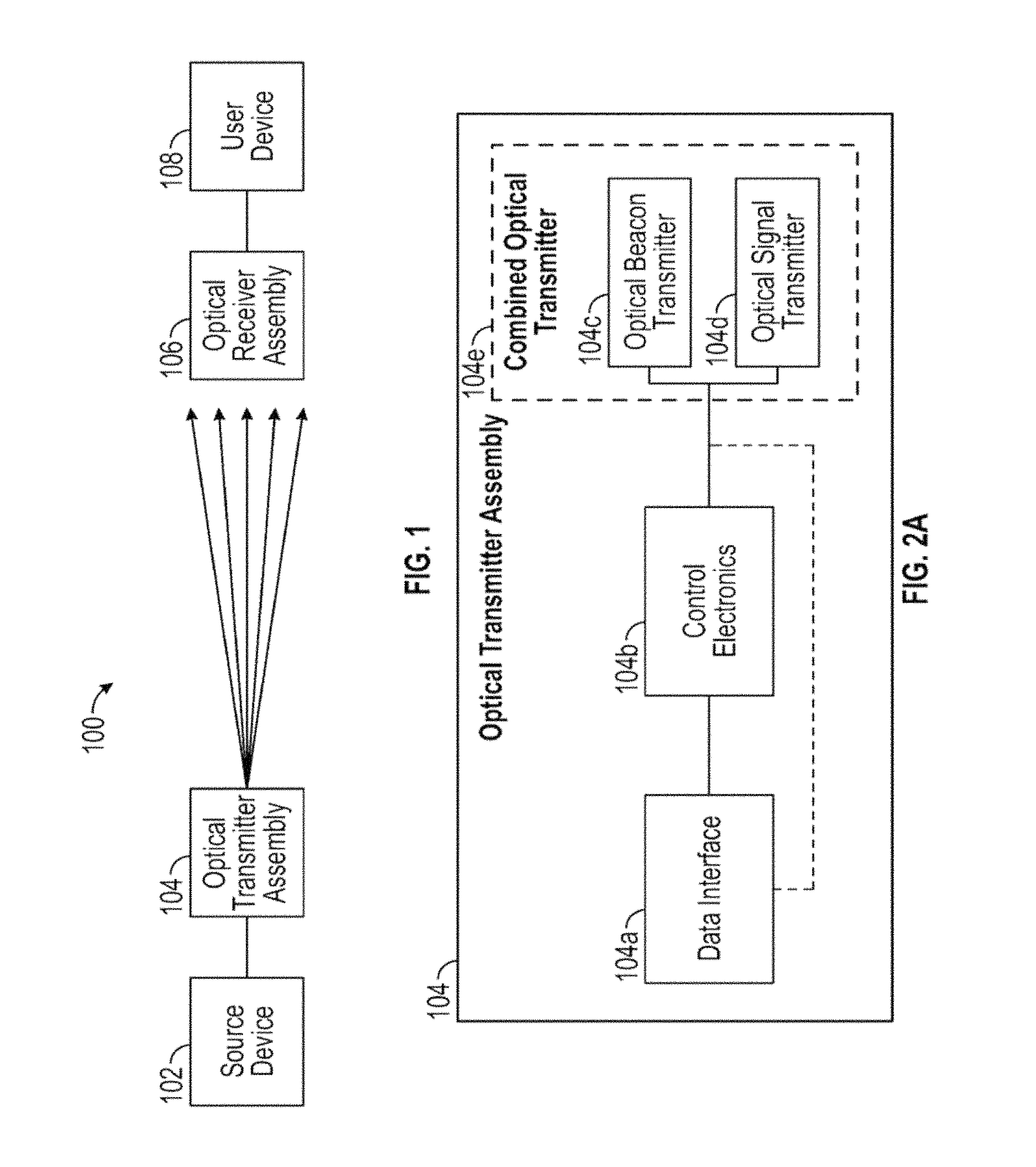
FIG. 1 illustrates an example optical narrowcasting system.
FIG. 2A illustrates example components that may make up an optical transmitter assembly.
FIG. 2B is a flow chart illustrating example operations that may be performed by the optical transmitter assembly of FIG. 2A and/or its component parts or elements.
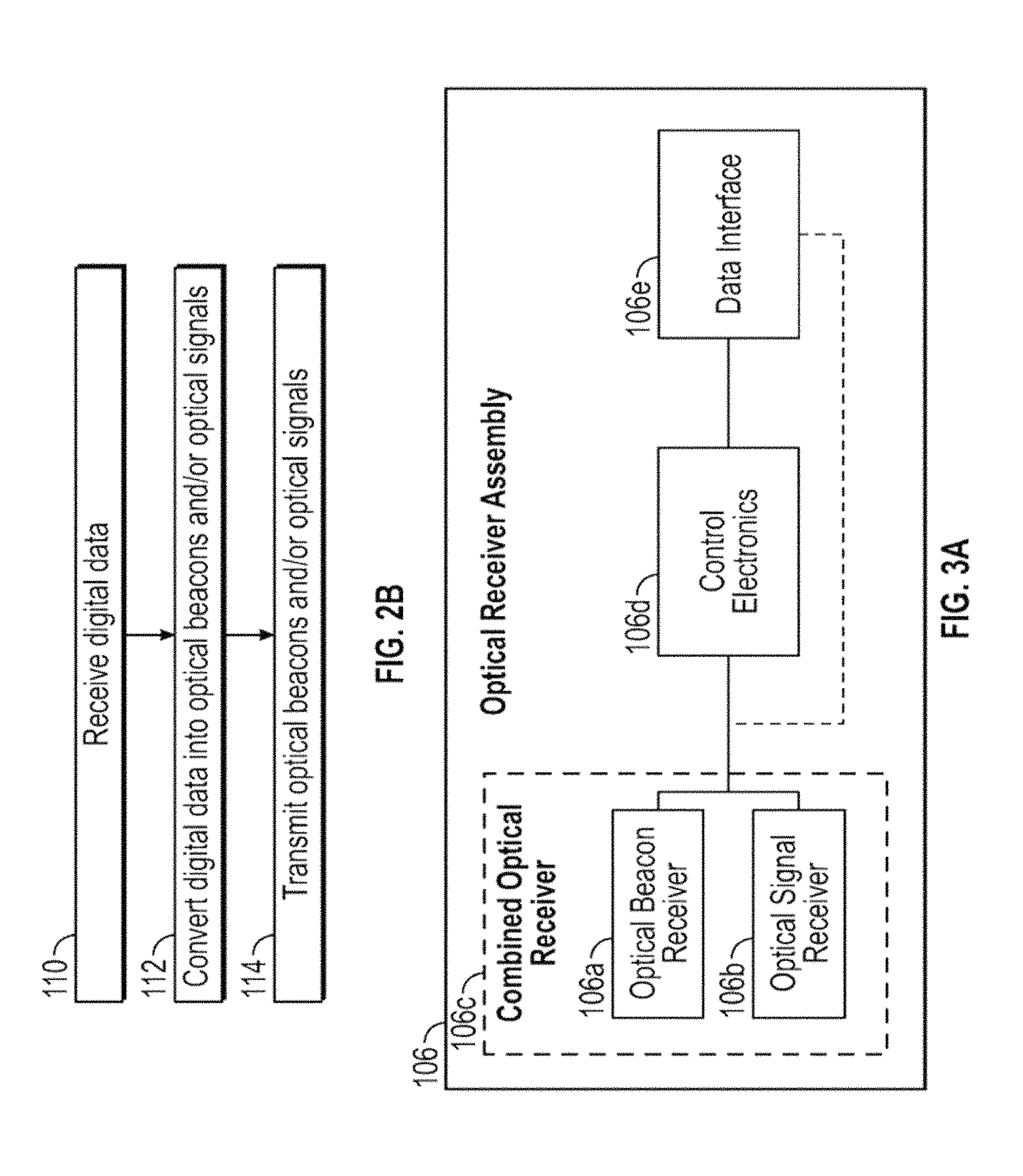
FIG. 3A illustrates an optical receiver assembly, including one or more example components that may make up the optical receiver assembly.
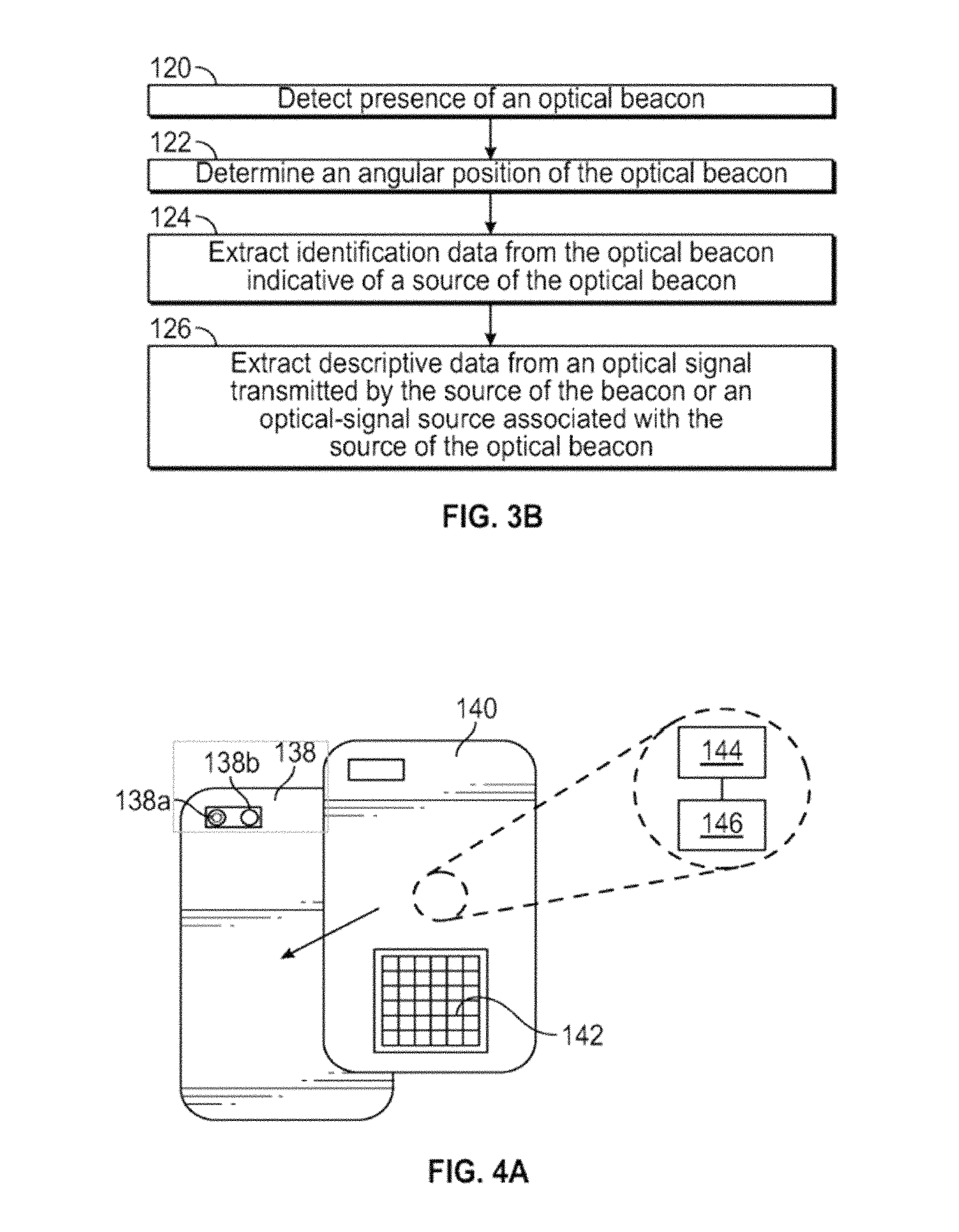
FIG. 3B is a flow chart illustrating example operations that can be performed by the optical receiver assembly of FIG. 3A and/or its component parts or elements.
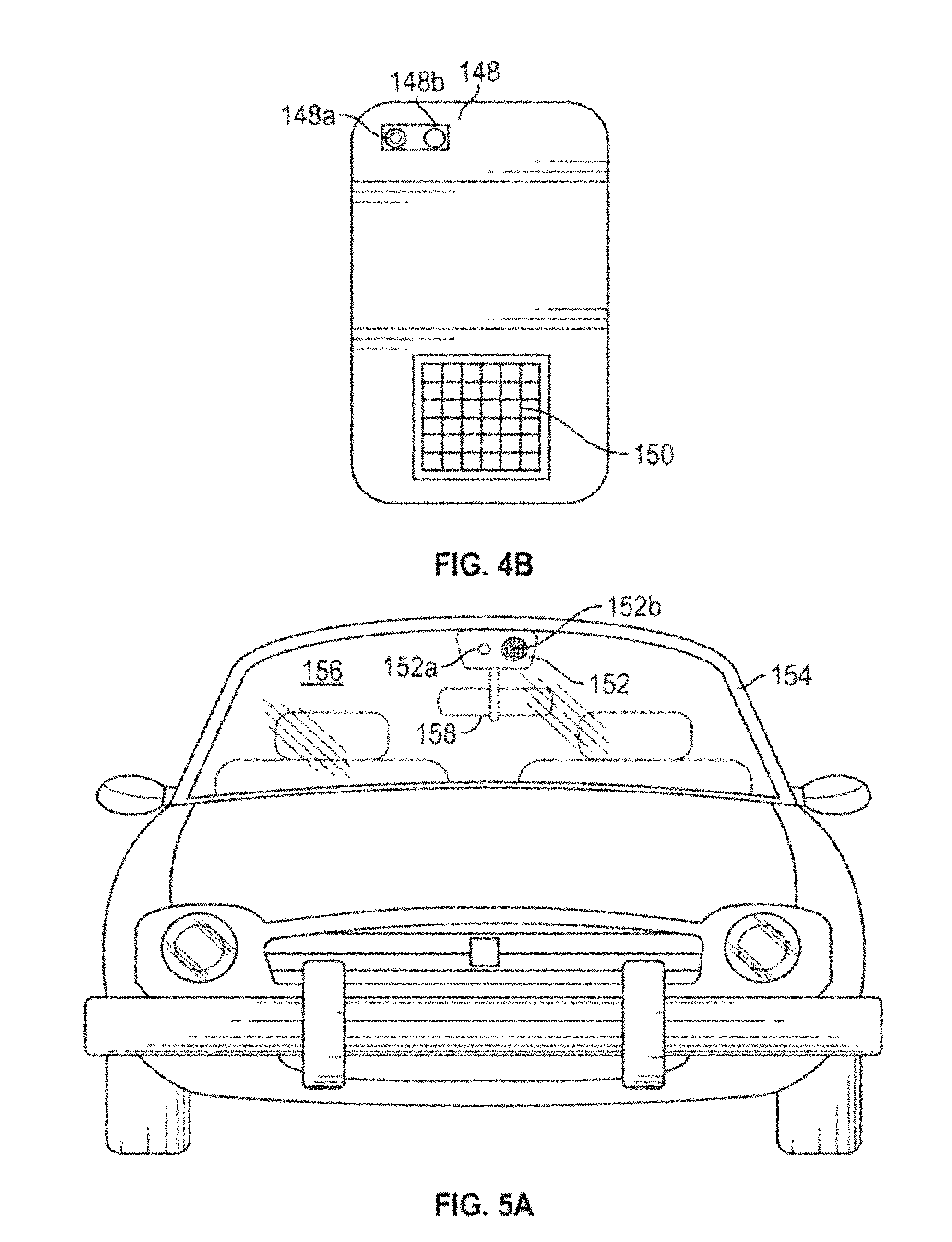
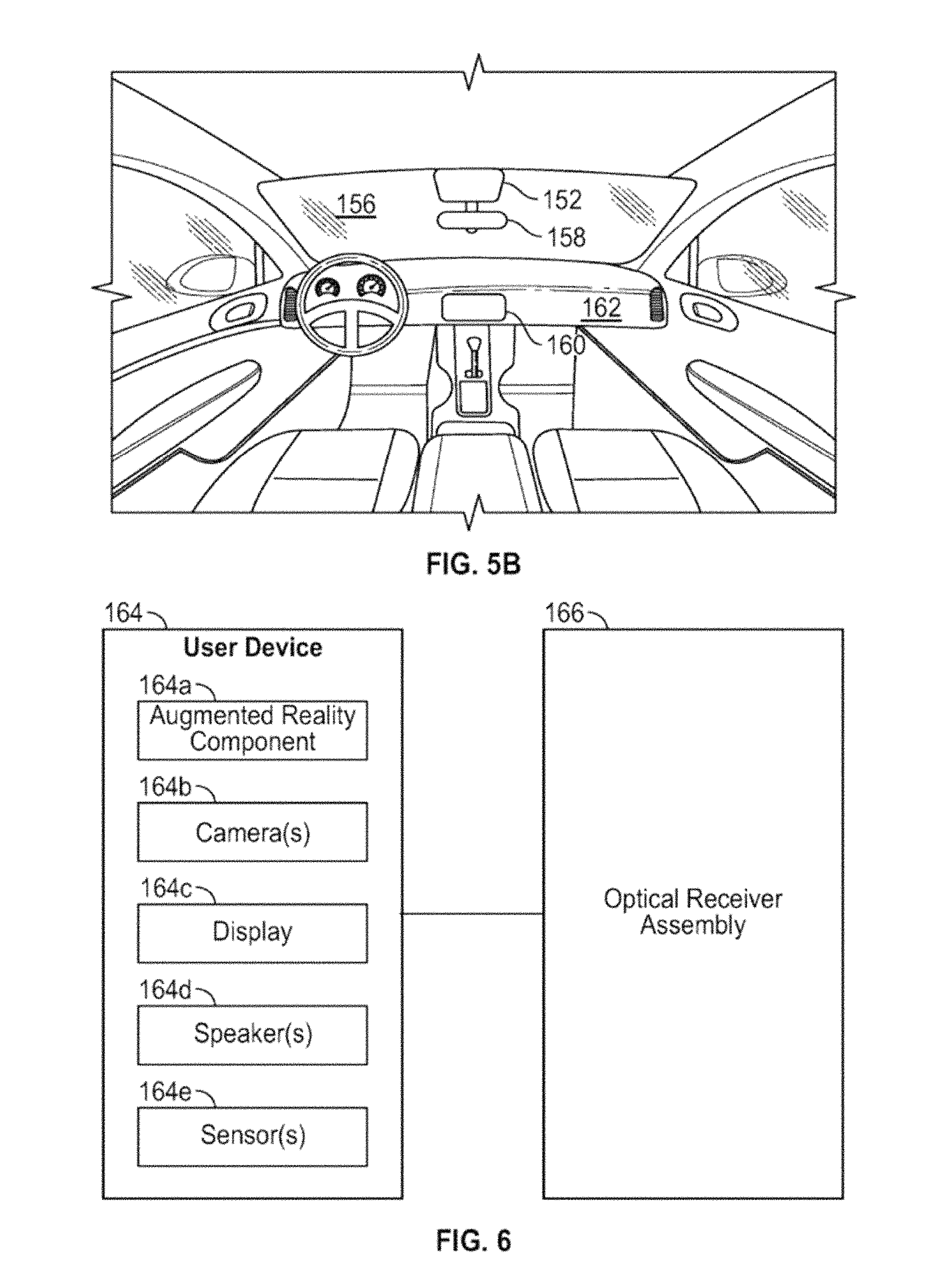
FIG. 4A illustrates an example of an optical receiver assembly attachment.
FIG. 4B illustrates an example of an optical receiver assembly that is incorporated into a device.
FIG. 5A illustrates a frontal view of an automobile in which an optical receiver assembly is installed in and electronically interfaced with a vehicle.
FIG. 5B illustrates an example interior view of the automobile of FIG. 5A.
FIG. 6 illustrates a user device that is operatively and/or communicatively connected to an optical receiver assembly.
FIG. 7 is a flow chart illustrating example operations that may be performed by a user/controlling device and optical receiver assembly within an optical narrowcasting system.
FIG. 8 is a depiction of an example optical transmitter assembly.
FIG. 9 depicts an example functional block diagram of an optical transmitter assembly.
FIG. 10 is a flowchart for optical narrowcast transmission of data in some embodiments.
FIG. 11 is a depiction of an example optical transmitter assembly.
FIG. 12a depicts a three-dimensional perspective view of beamforming optics with traced rays from a light source.
FIG. 12b depicts another three-dimensional perspective view of beamforming optics with traced rays from a light source.
FIG. 13 depicts a side view of an example beamforming optic with traced rays from a light source.
FIG. 14 is a cross-sectional view of an example axisymmetric reflective collimator.
FIG. 15 depicts a three-dimensional view of an example of a wineglass collimator for use in beamforming optics.
FIG. 16 depicts an example lenslet array.
FIG. 17 depicts an example pair of lenslet arrays.
FIG. 18a is a surface plot of the output intensity distribution as a function of a horizontal angle and a vertical angle produced by a single beamforming optic consisting of a wineglass collimator and lenslet arrays in some embodiments.
FIG. 18b is a surface plot of a portion of the combined output intensity distribution as a function of angle produced by six identical beamforming optics of the same type used to generate the results of FIG. 18a in some embodiments.
FIG. 19a is a graph of vertical slices taken through the center and at horizontal coordinates of .+-.4.degree. relative to the center of the same intensity distribution produced by a single beamforming optic in some embodiments that is depicted as a surface plot in FIG. 18a.
FIG. 19b is a graph of vertical slices taken through the center of the beam and at horizontal coordinates of .+-.4.degree. relative to the center of the same intensity distribution produced by the six beamforming optics in some embodiments that is depicted as a surface plot in FIG. 18b.
FIG. 20a is a graph of horizontal slices taken through the center of the beam and at vertical coordinates of .+-.3.95.degree. relative to the center of the same intensity distribution produced by a single beamforming optic in some embodiments that is depicted as a surface plot in FIG. 18a.
FIG. 20b is a graph of horizontal slices taken through the center of the beam and at vertical coordinates of .+-.3.95.degree. relative to the center of the same intensity distribution produced by the six beamforming optics in some embodiments that is depicted as a surface plot in FIG. 18b.
FIG. 21 depicts a simplified schematic diagram of an example OTA utilizing multiple light sources and beamforming optics.
FIG. 22 depicts an example of the optical power output (in arbitrary units) as a function of time for an optical beacon operating in the 800-900 nm band, as well as for an optical signal operating in the 900-1000 nm band, where the bit rates for the optical beacon and the optical signal are 333.33 kHz and 1 MHz, respectively.
FIG. 23 depicts three plots of temporal waveforms of transmitted output beams for an example of double modulation.
FIG. 24 is a block diagram of an example digital device.
FIG. 25 is a depiction of an example optical receiver assembly.
FIG. 26a schematically depicts an ORA that utilizes a single OSR and a single OBR.
FIG. 26b schematically depicts an ORA utilizing multiple OSRs.
FIG. 27 depicts a functional block diagram of an optical receiver assembly.
FIG. 28a is a flow diagram depicting a process of receiving optical signals by an optical receiver assembly.
FIG. 28b is a flow diagram depicting a process of receiving optical beacons by an optical receiver assembly.
FIG. 29a is a three-dimensional depiction of a detector and a beam of collimated rays traced through a lenslet, which focuses (i.e., concentrates) the rays onto the light-sensitive surface of a detector.
FIG. 29b depicts a three-dimensional view of an array of lenslets.
FIG. 30 depicts a diagonal cross-section (i.e., taken from one corner of the square entrance pupil to the corner on the opposite side) through an optical axis of an aspherical lenslet that may be used in an optical assembly.
FIG. 31a depicts a specification of an example detector.
FIG. 31b depicts a plot of the PIN-HR008 detector's spectral response.
FIG. 31c is a plot of the spectral response of an example optical bandpass filter that may be used in conjunction with the PIN-HR0080 detector to reduce detector noise due to background radiation.
FIG. 32 is a depiction of a photodiode array using PIN-HR0080 detectors with dimensions in millimeters.
FIG. 33 depicts the irradiance distribution produced on a single detector (e.g., one of the detectors in the detector array of FIG. 32) of the OSR using the lenslet array of FIG. 29b as an OSR optic when the incident beam from an optical transmitter is centered on the FOV of the OSR.
FIG. 34 depicts the irradiance distribution produced on a single detector when the transmitted beam is incident at an angle of 1.8.degree. (i.e., half the width of the OSR's FOV) relative to the center of the FOV.
FIG. 35A illustrates example irradiance distributions from an optical transmitter at different measurement planes;
FIG. 35B illustrates an example of positional and irradiance scaling in relation to far field optical beam irradiance.
FIG. 35C illustrates an example representation of optical beam intensity as a function of angular positioning.
FIG. 35D illustrates an example representation of optical beam intensity as a function of angular position when an optical transmitter is tilted or pointed in a particular direction.
FIG. 36A illustrates an example optical beam intensity distribution as a function of a horizontal angular position coordinate produced by an optical transmitter that outputs an optical beam with a constant intensity inside a rectangular angular region.
FIG. 36B illustrates the rectangular angular region within which the optical beam intensity distribution of FIG. 36A has constant intensity.
FIGS. 37A-B illustrate example optical beam intensity distributions from multiple optical transmitters.
FIG. 38A illustrates the optical beam intensity distribution as a function of a horizontal angular position coordinate produced by two output beams that are combined or tiled in accordance with various embodiments.
FIG. 38B illustrates the rectangular angular region within which the tiled optical beam intensity distribution of FIG. 38A has constant intensity.
FIG. 39 illustrates an example of the rectangular angular region within which a tiled optical beam has constant intensity in accordance with various embodiments.
FIG. 40A illustrates an example optical transmitter that can be used to produce a portion of a tiled optical beam in accordance with various embodiments.
FIG. 40B illustrates an example output beam that can be transmitted by the optical transmitter of FIG. 40A.
FIG. 41A illustrates an example of a multiple optical transmitter arrangement in accordance with one embodiment.
FIG. 41B illustrates a tiled optical beam in the far field that results from the optical transmitter arrangement of FIG. 41A.
FIG. 42A illustrates an example of a multiple optical transmitter arrangement.
FIG. 42B illustrates a side view showing the relative tilt between the optical transmitters of FIG. 42A.
FIG. 42C illustrates a perspective of a tiled optical beam resulting from the optical transmitter arrangement of FIG. 42A.
FIG. 43A illustrates a perspective representation of a multiple beamforming optics arrangement.
FIG. 43B illustrates a front view of the multiple beamforming optics arrangement of FIG. 43A.
FIG. 43C illustrates a side view of the multiple beamforming optics arrangement of FIG. 43A.
FIGS. 43D-F illustrate irradiance distributions produced by the multiple beamforming optics arrangement of FIGS. 43A-C at different distances from the exit pupils of the multiple optics.
FIG. 44 illustrates an example computing module that may be used to implement various features of the methods disclosed herein.
The figures are not exhaustive and do not limit the disclosure to the precise form disclosed.
DETAILED DESCRIPTION
Definitions
As used herein, an "optical narrowcasting system" or "ONS" is a system that can transmit information from one or more locations to one or more other locations using one or more digitally modulated optical beams transmitted through one or more propagation media. Contemplated propagation media may include, but are not limited to, air, water, glass windows, and the vacuum of space. An ONS may include one or more optical transmitter assemblies (OTAs) to transmit optical beams to one or more optical receiver assemblies (ORAS).
As used herein, an "optical beam" is a directed beam of electromagnetic radiation having wavelengths in a spectral region ranging from approximately 10 nm (e.g., extreme ultraviolet (UV) radiation) to approximately 10.sup.6 nm (e.g., far infrared (IR) radiation). As used herein to refer to an optical beam, the term "directed" beam can refer to energy, e.g., light energy sent in a specific range of propagation directions, but not in other directions. For example, a laser may emit a narrow directed beam of light, whereas the sun may be understood to emit undirected light that propagates outward in all possible directions.
As used herein, an "optical transmitter assembly" or "OTA" is a device including electronics, software (and/or firmware), and one or more optical transmitters (OTs). An OTA may be an element of an ONS. The OT(s) within an OTA can provide the functionality of at least one optical beacon transmitter (OBT) and/or at least one optical signal transmitter (OST). In some implementations, a single OT may function as both an OBT and an OST. In other implementations, the OBT(s) and OST(s) of an OTA can be separate devices. An OTA may also contain one or more tilt actuators allowing it to control the pointing direction(s) of the optical beam(s) output by its OT(s). An OTA's electronics and associated software (and/or firmware) may perform various useful functions, such as: providing an interface between the OTA and its user(s) (or its users' devices); supplying timing pulses and electrical power to its OT(s); controlling the operation of the OT(s) (e.g., turning them on and off, setting their data-transmission rate, etc.); transferring digital data to the OT(s) for them to output as one or more digitally modulated optical beams; and controlling one or more tilt actuators to alter the pointing direction(s) of the output optical beam(s).
As used herein, an "optical transmitter" or "OT" is a device including one or more optical sources, one or more beam-forming optics, and electronics with associated software (and/or firmware) adapted to transmit optical beams. One or more OTs may form at least part of an OTA. The optical sources may be coherent (e.g., lasers) or incoherent (e.g., light emitting diodes (LEDs)). The optical output of each optical source may be electronically modulated at a desired bit rate (or at one of a user-selectable range of bit rates) to transmit digital data in the form of a series of one-bits and zero-bits. The optical source(s) produce optical radiation in a desired optical waveband. Each beam-forming optic may collect flux emitted by one or more optical source(s) and utilize refraction, reflection, and/or diffraction to concentrate it into a transmitted beam having a desired angular intensity distribution. In some cases, the beam-forming optic may also include one or more spectral filters to minimize the amount of flux transmitted outside of the desired waveband. Multiple OTs could in some implementations be used in a single OTA to increase the solid angle of the output beam and/or to increase the output intensity in certain solid-angular regions. The electronics and associated software (and/or firmware) of an OT may perform the following functions: receive and (if necessary) modify timing pulses and electrical power sent to it by the OTA of which it is a component; receive and properly interpret various control signals sent to it from the OTA; and receive from the OTA, data in digital electronic form that it will then output in digital optical form.
As used herein, an "optical beacon transmitter" or "OBT" is a type of OT that produces a beacon associated with an OTA. An "optical beacon" or "beacon" is a modulated optical beam containing information that allows an ORA to detect the presence of an OTA. An optical beacon makes a user or entity receiving optically transmitted information aware of the presence or availability of information transmitted by the OTA associated with the beacon. In addition to detecting the presence of the OTA, a beacon produced by an OBT may also contain information allowing an optical receiver assembly (ORA) to identify the entity (e.g., business, organization, private individual, product, landmark, etc.) and type (i.e., category) of entity (e.g., restaurant, department store, movie theater, etc.) with which the OTA is associated. A beacon may also be used by an OBR to determine the angular position of the OTA. In some embodiments, the angular position, e.g., horizontal and/or vertical angular position, of the OTA can be determined based on information optically transmitted within or as part of the optical beacon. For example, latitudinal, longitudinal, and altitudinal information indicative of the location of an OTA may be transmitted in a beacon. In some embodiments, one or more measurements made by an OBR of the propagation direction of an optical beacon can be used by the OBR to derive, calculate, or otherwise determine an angular position of the OTA within the FOV of the OBR. As mentioned previously, a single OT within an OTA may function as both an OBT and an OST, or the OBT(s) and OST(s) within an OTA may be separate devices.
As used herein, an "optical signal transmitter" or "OST" is a type of OT that produces an optical signal associated with an OTA. An "optical signal" is a modulated optical beam containing information, other than information contained in an optical beacon, which the operators of an OTA desire to transmit to optical receiver assemblies (ORAs). The purpose of an OST is to transmit information to ORAs that have already detected the OTA of which the OST is a component. In some instances, the ORAs may have also identified and determined the angular location of the OTA prior to receiving optical signals transmitted by the OTA. A single OT within an OTA may function as both an OBT and an OST, or the OBT(s) and OST(s) within an OTA may be separate devices.
A modulated optical beam produced by an OTA may contain both optical beacons and optical signals. Alternatively, a modulated optical beam may contain only one or more optical beacons and no optical signals, or it may contain only one or more optical signals and no optical beacons. For example, an OTA may simultaneously output two separate optical beams, one being an optical beacon and another being an optical signal, where the optical beacon has a different wavelength spectrum than the optical signal.
As used herein, the term "optical information" generally refers to information extracted from a modulated optical beam or used to modulate an optical beam. Optical information may include identification data extracted from or contained in an optical beacon (e.g., identifying a particular OTA and/or source of the OTA) and descriptive data extracted from or contained in an optical signal (e.g., an advertisement or other message). This data may comprise machine-readable and/or human-readable data, such as text, video, audio, metadata, or other types of information.
As used herein, an "optical receiver assembly" or "ORA" is a device including electronics, software (and/or firmware), and one or more optical receivers (OR). The OR(s) within an ORA can provide the functionality of at least one optical beacon receiver (OBR) and/or at least one optical signal receiver (OSR). An ORA may be an element of an ONS. In some cases, an ORA may also contain one or more tilt actuators allowing it to control the directions from which its OBR(s) and OSR(s) can receive modulated optical beams. An ORA can perform one or more of the following functions. It may detect the presence of beacons transmitted by OTAs. It may extract information from beacons, such as the identities of the entities (e.g., businesses, organizations, private individuals, products, landmarks, etc.) with which OTAs are associated. It may determine the angular positions of OTAs by sensing the direction of incidence of beacons or extracting positioning information therefrom. It may receive and/or extract data from optical signals transmitted by OTAs. An ORA's electronics and associated software (and/or firmware) perform various useful functions, such as: providing an interface between the ORA and its user(s) (or its users' devices); supplying timing pulses and electrical power to its OBR(s) and OSR(s); controlling the operation of its OBR(s) and OSR(s) (e.g., turning them on and off, setting their data-reception rate, etc.); receiving and transferring to users (or to users' devices) information, such as identifying information and angular position, obtained by its OBR(s) regarding OTAs that have been detected; receiving and transferring to users (or to users' devices) data received from OTAs by its OSR(s); and controlling one or more tilt actuators to alter the pointing direction(s) of one or more OBRs and one or more OSRs.
As used herein, an "optical beacon receiver" or "OBR" is a device adapted to receive an optical beacon that may make up at least part of an ORA. An OBR may detect the presence of one or more OTAs. An OBR may also identify the entities (e.g., businesses, organizations, or private individuals) with which OTAs are associated through, e.g., information contained within an optical beacon, as well as determine the angular positions of OTAs. As noted previously, the angular positions of OTAs may be derived from measurement(s) of the propagation direction of a beacon and/or determined from information contained within the beacon. An OBR may include, for example: one or more optical detectors or detector arrays; one or more collection optics, each including one or more optical components (e.g., lenses, reflectors, and/or diffractive optical elements); and control electronics with associated software (and/or firmware). A spectral filter may be included in each collection optic to reduce to low levels the out-of-band flux incident on the detector(s). The optical detectors are capable of detecting optical flux in the waveband and at the bit rates of beacons which the OBR is designed to receive. In some cases an OBR could share some or all of its detectors, collection optics, electronic hardware, and software/firmware with one or more OSRs within the ORA of which it is a part. The electronics and associated software (and/or firmware) of an OBR perform at least the following functions: providing the means to receive and (if necessary) modify timing pulses and electrical power sent to it by the ORA of which it is a part; receiving and properly interpreting various control signals sent to it by the ORA; and transferring to the ORA information (e.g., identifying information and angular position) it has obtained regarding beacons it has detected and from which it has received information.
As used herein, an "optical signal receiver" or "OSR" is a device adapted to receive optical signals and to convert the data they contain into digital or electronic form. An OSR may include one or more optical detectors or detector arrays, one or more collection optics, and control electronics with associated software (and/or firmware). The optical detectors are capable of detecting optical flux in the waveband and at the bit rates of optical signals the OSR is designed to receive. Each collection optic can collect incident in-band flux over its entrance pupil and within its specified field of view (FOV), and utilizes refraction, reflection, and/or diffraction to concentrate it onto one or more of the optical detectors. A spectral filter may also be included in the optical train to reduce to low levels, the out-of-band flux incident on the detectors. In some cases, an OSR may share some or all of its detectors, collection optics, electronic hardware, and software/firmware with one or more OBRs within the ORA of which it is a part. The electronics and associated software (and/or firmware) of an OSR can perform one or more of the following functions: receive and (if necessary) modify timing pulses and electrical power sent to it by the ORA (of which it is a part); receive and properly interpret various control signals sent to it by the ORA; and transfer to the ORA, digital data extracted from optical signals it has received.
Disclosed herein are systems and methods of communication that utilize non-radio-wave-based communications channels. That is, communications may be achieved through the transmission and/or receipt of information in the form of modulated optical beams. In this way, a user or entity, such as a business wishing to transmit information, e.g., advertising information, may do so by utilizing an OTA that can convert a digital representation of the information into one or more modulated optical beams for transmission. It should be noted that the information transmitted may include information disseminated by businesses and other organizations, including government agencies, for example, and by individuals. Personal content, such as messages, photos, and videos shared by individuals within a social media context are other examples of information that may be transmitted.
A characteristic of the optical communications methods and systems disclosed herein is that a user of an ORA designed to receive information sent by one or more OTAs may not know ahead of time what specific optical transmitters will be sending information of interest to him/her or where they will be located. For this reason, one aspect of various embodiments is that an ORA may be equipped with one or more components adapted to detect the presence of optically transmitted information prior to receiving that information.
A user wishing to receive the information transmitted in the form of one or more modulated optical beams may utilize an ORA implemented within or in conjunction with a user device, such as a smartphone, to scan for and detect the presence of available optical beacons, extract the identifying information contained in the beacons, and display the identifying information through, e.g., an augmented reality (AR) interface. Upon selecting a specific OTA using information extracted from its associated beacon and displayed on the AR interface, the user, if he/she so desires, may further obtain some or all of the information contained within or represented by the optical signal associated with said OTA through the AR interface or other information-presentation mechanism, such as a media player (e.g., advertising information in the form of digital video).
Advantages can be realized by using such an optical communications system, referred to herein as an optical narrowcasting system. For example, optical narrowcasting systems such as those disclosed herein may have long-range, high-bandwidth capabilities, avoid regulatory limitations (optical transmissions are thus far unregulated by the Federal Communications Commission (FCC) or any other regulatory body). For example, optical narrowcasting systems can provide users with the ability to utilize existing hardware and/or software technologies that are enhanced by extremely compact non-imaging optical components that have low power needs and are energy efficient. For example, the operable range of an optical narrowcasting system can be approximately 400 m (e.g., during the day) to approximately 1200 m (e.g., during nighttime) compared to that of WiFi that is effective within approximately 50 m. Moreover, optical narrowcasting systems are able to direct information in one or more desired directions using, e.g., beamforming. This can be accomplished through the use of the aforementioned non-imaging optics, whereas directionality using WiFi is not practical given the need (of WiFi routers) to use expensive and bulky directional antennas. Regarding efficiency, optical narrowcasting networks can be up to 300 times more energy efficient than WiFi networks. Further still, the security that can be achieved in an optical narrowcasting network is much higher than that possible in a WiFi.RTM. network, due to the directionality of the transmitted optical beams.
FIG. 1 illustrates an example optical narrowcasting system 100. Transmitting and/or receiving an optical beam(s) may be accomplished using an OTA, e.g., optical transmitter assembly 104, and an ORA, e.g., optical receiver assembly 106. An noted previously, "optical transmitter assembly," or "OTA," may refer to an optical narrowcasting element adapted to transmit one or more optical beams, and can include certain electronics and/or circuitry, software and/or firmware, and one or more optical transmitters, which will be described in greater detail below with reference to FIG. 2. As illustrated in FIG. 1, optical transmitter assembly 104 may transmit one or more optical beams into a medium, such as air. As alluded to previously, an optical beam may comprise one or more of an optical beacon and an optical signal.
Optical transmitter assembly 104 may receive, modulate, convert, and/or otherwise process digital information into an optical format for transmission as an optical beam to be received by optical receiver assembly 106. The digital information may be received by optical transmitter assembly 104 from one or more sources, e.g., source device 102. Source device 102 may be a computer tablet, smartphone, data server, or other information source.
Optical transmitter assembly 104 may be installed on various fixed structures, such as buildings, billboards, road signs, and the like. It may also be installed on vehicles such as automobiles and buses. It should be understood that these installations are merely examples and not limiting in any way. Optical transmitter assembly 104 may also be incorporated into portable and/or handheld devices, such as smartphones, tablet computers, and head mounted displays, or it may be incorporated into devices intended to be attached to, or kept in close proximity to, portable and/or handheld devices, such as smartphone cases and cases for tablet computers. It should be understood that the devices mentioned here are merely examples and not limiting in any way. Moreover, although optical transmitter assembly 104 is illustrated as being associated with a single source device 102, optical transmitter assembly 104, in some embodiments, may be associated with and/or receive digital information from additional source devices.
Optical receiver assembly 106 may be installed on various fixed structures, such as buildings, billboards, road signs, and the like. It may also be installed on vehicles such as automobiles and buses. It should be understood that these installations are merely examples and not limiting in any way. Optical receiver assembly 106 may also be incorporated into portable and/or handheld devices, such as smartphones, tablet computers, and head mounted displays, or it may be incorporated into devices intended to be attached to, or kept in close proximity to, portable and/or handheld devices, such as smartphone cases and cases for tablet computers. It should be understood that the devices mentioned here are merely examples and not limiting in any way. Moreover, although optical receiver assembly 106 is illustrated as being associated with a single user device 108, optical receiver assembly 106, in some embodiments, may be associated with, controlled by, and/or share digital information with additional user devices.
Optical receiver assembly 106 may be an optical narrowcasting element adapted to receive one or more optical beams, and can include certain electronics and/or circuitry, software and/or firmware, and one or more optical receivers, which will be described in detail below with reference to FIG. 4. Optical receiver assembly 106 may receive an optical beam and demodulate, convert, and/or otherwise process the optical beam back into digital information. Optical receiver assembly 106 may transmit or forward the digital information to a receiving device, such as user device 108. User device 108 may be a computer tablet, smartphone, network server, or other device capable of receiving and/or utilizing the digital information or data. Optical receiver assembly 106 may be integrated with user device 108 or optical receiver assembly 106 may be operatively attached to user device 108. It should be noted that optical receiver assembly 106 need not be associated with only a single user device. In some embodiments, optical receiver assembly 106 may transmit or forward received digital information to more than one user device, e.g., via broadcasting, multicasting, etc.
It should be noted that although FIG. 1 depicts one-way communications between optical transmitter assembly 104 and optical receiver assembly 106, an optical narrowcasting system may also involve two-way communications. For example, source device 102 and user device 108 may each have respective optical transmitter and optical receiver assemblies integrated therein or operatively attached thereto. Optical beams may, in some cases, be in the visible or near-IR bands. Optical beams may be produced using either incoherent sources (e.g., light emitting diodes (LEDs)), lasers, or other appropriate light sources. Depending on the application, different angular beam widths can be used. Optical beams may either propagate from an optical transmitter assembly directly to an optical receiver assembly along an unobstructed line of sight (LOS), or optical beams may propagate along an indirect, non-LOS path, utilizing diffuse reflections from ceilings, walls, or other structures, for example, or from suspensions of small particles (e.g., airborne dust) or liquid droplets (e.g., clouds or fog). As illustrated in FIG. 21, two or more identical modular transmitter-optics units may be used to produce combined beams having increased horizontal and/or vertical angular beam widths, and/or increased intensity within certain solid-angular regions.
An ad hoc network (e.g., a communications network established directly between two or more computers or other devices) need not rely on a base station or other centralized access point. Such communications networks are generally established on a temporary basis between a small number of participants in close physical proximity for a specific common purpose, such as sharing a set of documents being written by the participants or playing multi-player computer games. In some embodiments, two or more user devices (one embodiment of which can be user device 108) may each comprise optical transmitter assemblies and optical receiver assemblies (embodiments of which can be optical transmitter assembly 104 and optical receiver assembly 106 of FIG. 1). The two or more user devices may be used to transmit and receive data via optical beams, thereby creating an ad hoc optical narrowcasting network.
FIG. 2A illustrates example components that may make up optical transmitter assembly 104. Optical transmitter assembly 104 may include a data interface 104a. Data interface 104a may comprise electronics and/or circuity, as well as associated software (and/or firmware) adapted to provide an interface between optical transmitter assembly 104 and source device 102 (and/or a user of source device 102). For example, optical transmitter assembly 104 may be controlled by source device 102 via data interface 104a. Data interface 104a may communicate with source device 102 by way of a hardwired and/or wireless (e.g., Bluetooth.RTM.) connection. One or more software applications on source device 102 may allow data files to be uploaded to a memory unit of optical transmitter assembly 104 via data interface 104a. These one or more software applications may also allow a user to send commands instructing optical transmitter assembly 104 to optically transmit the contents of one or more data files that have been uploaded to optical transmitter assembly 104. The user may also be able to specify values, such as bit rate, optical output intensity, pulse duty cycle, and other relevant operating parameters for optical transmitter assembly 104.
Optical transmitter assembly 104 may include control electronics 104b. Control electronics 104b may receive the above-noted values that have been input by the user and utilized to control operation of optical transmitter assembly 104. For example, control electronics 104b may supply timing pulses and electrical power to the optical transmitters, control the operation of one or more optical transmitters, e.g., optical beacon transmitter 104c and optical signal transmitter 104d, (for example, by turning them on and off, setting their data-transmission rate, etc.). Control electronics 104b may effectuate the transfer of digital data to one or more of the optical transmitters to be output as one or more digitally modulated optical beams.
In some embodiments, optical transmitter assembly 104 may also comprise one or more tilt actuators, such as microelectromechanical systems (MEMS) actuators, that allow optical transmitter assembly 104 to control direction(s) in which one or more optical beams may be pointed upon being output. For example, optical beacon transmitter 104c, optical signal transmitter 104d, and/or combined optical transmitter 104e may be mounted or otherwise incorporated into optical transmitter assembly 104 via a connection that allows for the one or more tilt actuators to move the transmitters. Control electronics 104b may control operation of the one or more tilt actuators.
Optical transmitter assembly 104 may include one or more optical transmitters adapted to process digital information received from, e.g., source device 102, for transmission as an optical beam. As illustrated in FIG. 2A, some embodiments may have an optical beacon transmitter 104c and an optical signal transmitter 104d. Optical beacon transmitter 104c may be adapted to transmit optical beacons that are specifically intended to be received by optical beacon receivers. Optical beacons allow the presence of optical transmitter assembly 104 to be detected. Optical beacons may allow the source (e.g., user or entity associated with source device 102, source device 102, and/or optical transmitter assembly 104) to be identified. Optical beacons may also allow the horizontal and/or vertical angular position of the optical transmitter assembly 104 within the FOV of an OBR at a different location to be determined. This can be accomplished, for example, by an OBR utilizing a lens, such as an imaging lens, to concentrate (i.e., focus) optical beacons incident on the lens from different directions onto correspondingly different locations on a detector array located in the focal plane of the lens. The location in the detector array at which an optical beacon is currently focused can be a measure of the current angular position relative to the OBR's FOV of the OTA from which the optical beacon is transmitted. That is, optical power in the form of an optical beacon may be currently, primarily or entirely, concentrated (by the OBR's lens) onto a detector located at a particular row and column of the detector array used in the OBR. The OBR may be a camera that is sensitive to the waveband of the optical beacon. The row and column of the detector array at which the optical beacon is concentrated can be a current estimated location (within the FOV of the OBR) of the OTA that sent the beacon. OTA locations in this form can be mapped to analogous locations within the FOV of an associated visible-light camera, such as the forward-looking camera of a smartphone. This allows the locations of OTAs to be represented on a user's real-time video display (e.g., that of the smartphone). An icon representing the OTA can then, for example, be overlaid at this location in the real-time video display. It should be noted that the horizontal and vertical angular location of an OTA can in general, be a function of time. For example if an OTA moves due to it being mounted on a vehicle that moves, its location within the FOV of an OBR may change. Similarly, if the ORA moves to a new location and/or is tilted, the OTA location within the FOV of the OBR may also change, even though the OTA has stayed in the same physical location.
Optical signal transmitter 104d may be adapted to transmit optical signals specifically intended to be received by optical signal receivers. Optical signals transmit information from optical transmitter assembly 104 to optical receiver assembly 106, where optical transmitter assembly 104 and/or an entity associated with it may have already been detected, identified, and whose horizontal and/or vertical angular position relative to the FOV of an OBR has already been determined. Moreover, two or more optical transmitters may be implemented in optical transmitter assembly 104 to increase the solid angle of an output optical beam and/or to increase output intensity in certain solid-angular regions.
As also illustrated in FIG. 2A, an alternative may be to utilize a "combined" optical transmitter 104e that realizes the functionality of both optical beacon transmitter 104c and optical signal transmitter 104d. For example, combined optical transmitter 104e may comprise a single optical transmitter adapted to transmit both optical beacons and optical signals. That is, combined optical transmitter 104e may be designed to transmit an optical beam intended to be received both by optical beacon receivers and by optical signal receivers.
An optical transmitter, e.g., optical beacon transmitter 104c, optical signal transmitter 104d, and/or combined optical transmitter 104e, may include one or more optical sources, one or more beam-forming optics, as well as electronics with associated software and/or firmware (see FIG. 9). The optical sources may be coherent (e.g., lasers) or incoherent (e.g., LEDs). The optical output of each optical source may be electronically modulated at a desired bit rate (or at one of a user-selectable range of bit rates) to transmit digital information in the form of a series of one-bits and zero-bits. The optical source(s) may produce optical radiation in a desired optical waveband. Each beam-forming optic can collect flux emitted by the one or more optical sources and utilizes refraction, reflection, and/or diffraction to concentrate it into a transmitted beam having a desired angular intensity distribution. In some cases, a beam-forming optic may include one or more spectral filters to minimize the amount of flux transmitted outside of a desired waveband.
The electronics and associated software (and/or firmware) of an optical transmitter, e.g., optical beacon transmitter 104c, optical signal transmitter 104d, and/or combined optical transmitter 104e, may perform one or more of the following functions: receiving and, if necessary, modifying timing pulses and/or electrical power received from optical transmitter assembly 104; receiving and properly interpreting various control signals sent to it from optical transmitter assembly 104; and receiving, from, e.g., data interface 104a by way of control electronics 104b, information or data in digital form that it will then output in digital optical form vis-a-vis an optical beam. It should be noted that in some embodiments, digital information or data may be received directly from data interface 104A.
FIG. 2B is a flow chart illustrating example operations that may be performed by optical transmitter assembly 104 and/or its component parts or elements. At operation 110, digital data to be optically transmitted may be received by optical transmitter assembly 104. As described above, the digital data to be optically transmitted may be received via data interface 104a. For example, a user, through source device 102 may upload a digital video advertisement to optical transmitter assembly 104. At operation 112, the digital data may be converted into one or more optical beacons and/or optical signals. For example, the digital video advertisement may be converted into an optically formatted representation of the digital video advertisement for transmission in the form of an optical signal. This operation is described in greater detail with respect to Fig. FIG. 9, and may involve performing one or more conversion, processing, and/or modulation operations at one or more of optical beacon transmitter 104c, optical signal transmitter 104d, and/or combined optical transmitter 104e under the control of control electronics 104b. At operation 114, the optical beacons and/or optical signals are transmitted by one or more of optical beacon transmitter 104c, optical signal transmitter 104d, and/or combined optical transmitter 104e. In the case of an optical beacon, information identifying, e.g., the user of source device 102, may be transmitted with the optical signal or converted into an optical beacon that is transmitted separately.
FIG. 3A illustrates optical receiver assembly 106 in more detail including one or more example components that may make up optical receiver assembly 106. For example, optical receiver assembly 106 may include one or more of an optical beacon receiver 106a, and an optical signal receiver 106b, or as an alternative, a "combined" optical receiver 106c that realizes the functionality of both optical beacon receiver 106a and optical signal receiver 106b. For example, combined optical receiver 106c may comprise a single optical receiver adapted to receive both optical beacons and optical signals.
In some embodiments, similar to optical transmitter assembly 104, optical receiver assembly 106 may include one or more tilt actuators allowing optical receiver assembly 106 to control the direction(s) from which its optical beacon receiver(s) and/or optical signal receiver(s) may receive optical beams transmitted by one or more optical transmitter assemblies, e.g., optical transmitter assembly 104.
The purpose of optical receiver assembly 106, as alluded to previously, may be to detect the presence of and/or receive data (in the form of optical beacons and/or optical signals) transmitted by optical transmitter assembly 104. For example, optical receiver assembly 106 may detect the presence of optical transmitter assemblies by detecting optical beacons sent by them, extract identifying information from optical beacons regarding, e.g., entities associated with the optical transmitters that sent the optical beacons, determining horizontal and/or vertical angular positions of optical transmitter assemblies (by sensing the direction of incidence of the optical beacons), and receiving information or data in the form of optical signals.
Optical receiver assembly 106 may comprise a data interface 106e that provides an interface between the optical receiver assembly and one or more users and/or user devices, e.g., user device 108. Data interface 106e may be responsible for receiving and transferring to users (or to users' devices, e.g., user device 108) information, such as identifying information and horizontal and/or vertical angular positions obtained by optical beacon receiver 106a regarding detected optical beacons. Data interface 106e may be responsible for receiving and transferring to users (or to users' devices, e.g., user device 108) data received via an optical signal by optical signal receiver 106a, for example. Optical receiver assembly 106 may be interfaced with user device 108 by way of a wired or wireless connection via data interface 106e. Software resident on user device 108 may be utilized by a user to operate optical receiver assembly 106. Additionally, the user may be able to specify the range of bit rates for signals to be received, error-correction methods to be used, and/or various other receiver operating parameters using user device 108, where the operating parameters may be transmitted to optical receiver assembly 106 via data interface 106e.
Optical receiver assembly 106 may comprise control electronics 106d. Control electronics 106d may supply timing pulses and electrical power to optical beacon receiver 106a, optical signal receiver 106b, or alternatively, to combined optical receiver 106e. Control electronics 106d may control the operation of optical beacon receiver 106a, optical signal receiver 106b, or alternatively, combined optical receiver 106e (e.g., turning them on and off, setting the data-output format, etc.). Data interface 106e may control the one or more tilt actuators that can be used to alter the direction(s) in which of one or more optical beacon receivers and/or one or more optical signal receivers may be pointed.
Optical beacon receiver 106a and/or combined optical receiver 106c may be adapted to detect the presence of one or more transmitted optical beams, distinguishing them from incident in-band radiation produced by radiation sources other than optical transmitters of an optical narrowcasting system (e.g., natural and artificial illumination sources). Optical beacon receiver 106a and/or combined optical receiver 106c may be configured to determine a horizontal and vertical angular position of one or more transmitted optical beams within its field of view (FOV). Optical beacon receiver 106a and/or combined optical receiver 106c may receive identifying information from one or more optical transmitter assemblies, e.g., optical transmitter assembly 104, whose optical beacons it has detected and received. For example, an optical transmitter assembly operated by a restaurant may transmit an optical beacon containing the (digitally encoded) name of the restaurant and/or type of restaurant in a format intended to be received by optical beacon receiver 106a and/or combined optical receiver 106c.
Optical beacon receiver 106a and/or combined optical receiver 106c may include one or more optical detectors or detector arrays, one or more collection optics, each including one or more optical components (e.g., lenses, reflectors, and/or diffractive optical elements), as well as its own control electronics with associated software (and/or firmware). A spectral filter may be included in each collection optic to increase communication range by reducing to low levels the out-of-band flux incident on the detector(s). Optical beacon receiver 106a and/or combined optical receiver 106c may be capable of detecting optical flux in the waveband and at the bit rates used by optical transmitters to transmit optical beacons it is designed to detect. The component parts of optical beacon receiver 106a and/or combined optical receiver 106c are described in greater detail with respect to FIGS. 26-27.
In some cases, an optical beacon receiver may share some or all of its detectors, collection optics, electronic hardware, and software/firmware with one or more optical signal receivers, an embodiment of which may be combined optical receiver 106c. The electronics and associated software (and/or firmware) of optical beacon receiver 106a and/or combined optical receiver 106c can perform at least one or more of the following functions: receive and (if necessary) modify timing pulses and electrical power sent to it by optical receiver assembly 106; receive and properly interpret various control signals sent to it by optical receiver assembly 106; and transfer to optical receiver assembly 106, information (e.g., identifying information and angular position) it has obtained regarding optical beacons it has detected.
Optical signal receiver 106b and/or combined optical receiver 106c may receive optical signals from one or more optical transmitter assemblies, e.g., optical transmitter assembly 104. Optical signal receiver 106 and/or combined optical receiver 106c may convert the optically formatted digital data into digital data in electronic form. Similar to optical beacon receiver 106a, optical signal receiver 106b and/or combined optical receiver 106c may include one or more optical detectors or detector arrays, one or more collection optics, and control electronics with associated software (and/or firmware). In the case of combined optical receiver 106c, the component parts of optical beacon receiver 106a may be adapted to also operate as an optical signal receiver. The optical detectors can detect optical flux in the waveband and at the bit rates used by optical transmitters to transmit optical signals and/or optical beacons it is designed to receive. Each collection optic may collect incident in-band flux over its entrance pupil and within its specified FOV, and utilize refraction, reflection, and/or diffraction to concentrate it onto one or more of the optical detectors. A spectral filter may also be included in each receiver optic to increase communication range by reducing the out-of-band flux incident on the detectors to lower levels.
It should be noted that one or more of the aforementioned optics and/or detectors or detector arrays that, in part, make up optical beacon receiver 106a, optical signal receiver 106b, and/or combined optical receiver 106c may be custom manufactured and/or commercially available. For example, one or more refractive optics may be customized with respect to one or more optical characteristics or properties such that its operation may be optimized for use in optical receiver assembly 106. For example, one or more optical detectors or detector arrays may be commercially available near-IR detectors or detector arrays.
The electronics and associated software (and/or firmware) of optical signal receiver 106b and/or combined optical receiver 106c can perform one or more of the following functions: receive and (if necessary) modify timing pulses and electrical power sent by the optical receiver assembly 106; receive and properly interpret various control signals sent to it by optical receiver assembly 106; and transfer digital data received from one or more optical transmitters, e.g., optical signal transmitter 104d and/or combined optical transmitter 106e, to optical receiver assembly 106. In some embodiments, the electronics and associated software (and/or firmware) may be customized to provide appropriate electrical power to operate the optical detectors. Moreover, it should be noted that electronics hardware and/or software may continuously monitor the output of the optical detectors, determining when an output therefrom may represent a signal sent by an optical transmitter--as opposed to, for example, flux received from artificial or manmade illumination sources.
Once an optical beacon has been detected, optical receiver assembly 106 may receive a related optical signal and store it as a data file in its memory. For example, optical receiver assembly 106 may buffer its detector outputs using one or more memory units or memory partitions to permit at least a portion of a given optical signal to be received prior to it being recognized as an actual optical signal. Alternatively, optical transmitter assembly 104 may transmit an optical signal that contains at its beginning, a short "alert"-pulse sequence. This alert-pulse sequence may inform optical receiver assembly 106 that transmission of an optical signal dataset has begun, thereby allowing it to store the entire dataset in its memory, without the need for buffering. That is, optical beacon transmitter 104c of optical transmitter assembly 104 may transmit an optical beacon followed by an optical signal that begins with an alert-pulse sequence. These operations may be continuously repeated by optical transmitter assembly 104. In some embodiments, each transmitted optical beacon may end with an alert-pulse sequence, rather than having an alert-pulse sequence be included at the beginning of each transmitted optical signal.
FIG. 3B is a flow chart illustrating example operations that can be performed by an optical receiver assembly, e.g., optical receiver assembly 106 and/or its component parts or elements. At operation 120, optical receiver assembly 106 may detect the presence of an optical beacon that can be transmitted by optical transmitter assembly 104. As previously discussed, an optical beacon may be an optical beam comprising information identifying a source of the optical beacon. An optical beacon may also allow an optical receiver assembly 106 to estimate the horizontal and vertical angular position of its associated optical transmitter assembly relative to the FOV of one or more optical beacon receivers comprising part of the optical receiver assembly 106. At operation 122, the angular position of the optical beacon relative to the FOV(s) of one or more optical beacon receivers is determined based on its incident propagation direction. Because a plurality of optical beacons and/or optical signals may be transmitted within optical narrowcasting system 100, the angular position of an optical beacon transmission may be utilized to point or focus optical signal receiver 106b or combined optical receiver 106c in the direction of optical transmitter assembly 104 from where the optical beacon and associated optical signal(s) may originate. The angular position of an optical beacon transmission may also be utilized for other purposes, such as to assist a user in navigating to a location at which an OTA is located. At operation 124, the identification information may be extracted from the optical beacon, the identification information being indicative of or otherwise identifying the source of the optical beacon. In this context, the source of the optical beacon may be optical transmitter assembly 104, source device 102 and/or a user or entity utilizing source device 102 to transmit optical beams via optical transmitter assembly 104. At operation 126, information sent in the form of an optical signal by the source of the optical beacon may be extracted. Again, the source of an optical signal and the source of an optical beacon with which it is associated may be one in the same, e.g., source device 102 or optical transmitter assembly 104, or alternatively a user or entity utilizing source device 102 to transmit optical beams via optical transmitter assembly 104.
In some embodiments, optical narrowcasting system elements, such as optical receiver assemblies, may be integrated into a device, e.g., user device 108. That is, user device 108 may have resident optical receiver functionality. Alternatively, optical receiver assemblies may be operatively and communicatively connected to user device 108. In this case, an optical receiver assembly may be added to user device 108 as an attachment or enhancement. The same can be true for optical transmitter assemblies, although, in some cases, optical transmitter assemblies may be "stand-alone" elements that are fixed at a particular location.
FIG. 4A illustrates an example of an optical receiver assembly attachment. In the illustrated embodiment, optical receiver assembly 142 may be incorporated into a user device case 140 for user device 138 (e.g., a smartphone case for a smartphone device). It should be noted that the "visible" aspects of optical receiver assembly 142 may include one or more optical receiver elements, such as one or more lenses or lenslet arrays and one or more optical detectors. For example, optical receiver assembly 142 of FIG. 4A may include a lenslet array and detectors, each lenslet in the array having an optical detector in its focal plane. It should be noted that the optical detectors are not visible in FIG. 4A because they are hidden behind the lenslets. Other components parts of optical receiver assembly 142 may be incorporated into user device case 140, but may not be visible when user device case 140 is placed on user device 138.
FIG. 4B illustrates an example of an optical receiver assembly that is incorporated into a device. In particular, optical receiver assembly 150 may be incorporated directly into user device 148. For example, during the manufacturing of user device 148, optical receiver assembly 150 may be installed. Again, although only visible aspects of optical receiver assembly 150 are shown, other components of optical receiver assembly 150 may be incorporated into user device 148 within the housing of user device 148.
As alluded to previously, a user may utilize a device to interact with an optical receiver assembly to input operating parameters, receive transmitted data, control the optical receiver assembly, etc. The software/software applications may be utilized by the user to manage messages received optically. In addition, if the user is a subscriber of a social media service, the controlling software may allow the user to access all of the capabilities of that service, such as posting optically received messages, images, videos, or other information on a social media "page," viewing and responding to posts on other users' pages, sharing posts, etc., in the usual manner in which such tasks are performed within the context of social media services.
To that end, FIG. 4A illustrates that user device case 140 may also include one or more communications elements that allow user device 138 and optical receiver assembly 142 to communicate and/or interact. For example, as described above, user device 138 may be utilized by a user to input operating parameters for optical receiver assembly 142, etc. As illustrated in FIG. 4A, one such communications element 144 may be a Bluetooth.RTM. transceiver, an NFC transceiver or other communications element. If needed, a power supply 146 (e.g., a compact battery, an energy harvesting sensor, or other appropriate power source) may be provided to energize communications element 144. Here, communications element 144 and power supply 146 may embedded in or located on the device-facing side of case 140 for aesthetics and/or to gain closer operating proximity to user device 138. It should be noted that power supply 146 may also provide power to optical receiver assembly 142, or optical receiver assembly 142 may have its own power source that can be used to power communications element 144. In some embodiments, optical receiver assembly 142 and/or communications element 144 may be integrated into a single unit or device that may be attached to an input/output port, such as a micro-USB or Lightning port of user device 138.
In the case of user device 148, a user may control optical receiver assembly 150 and/or perform the above-noted functions and/or interactions via a hardwired connection between optical receiver assembly 150 and one or more processors, memory units, and/or other applicable components of user device 148, which may be an embodiment of a computing component illustrated in FIG. 60.
FIGS. 5A and 5B depict a contemplated implementation where an optical receiver assembly 152 may be installed in and electronically interfaced with a vehicle. FIG. 5A illustrates a frontal view of an automobile 154 in which an optical receiver assembly 152 is installed in automobile 154 near a top portion of windshield 156 above rearview mirror 158. Optical receiver assembly 152 may be attached to the outside of windshield 156 or on an inside surface of windshield 156. In the latter case, optical receiver assembly 152 may receive optical beacons and/or optical signals that have passed through windshield 156. Although optical receiver assembly 152 is shown to be mounted near the top of windshield 156 and above rearview mirror 154, optical receiver assembly 152 may be mounted on a different part of windshield 156 or on another part of automobile 154 entirely (e.g., on its roof) so long as it is in a position to receive one or more optical beams.
Optical receiver assembly 152 may include an optical beacon receiver 152a and an optical signal receiver 152b, as well as any electronics and/or software (and/or firmware), e.g., the aforementioned control electronics, data interface, etc. utilized in operating optical receiver assembly 152 and/or communicating with, e.g., media and/or information systems resident in a vehicle such as a vehicle's navigation system, media, system, heads-up display, etc. It should be noted that the electronics and software/firmware are not visible in the frontal view depicted in FIG. 5A, but are nevertheless present in optical receiver assembly 152 and/or in an associated component(s). In some embodiments, optical beacon receiver 152a and optical signal receiver 152b may share some or all of their optical components and optical detectors or detector arrays.
FIG. 5B illustrates an example interior view of automobile 154 of FIG. 5A. In FIG. 5B, a back or rear portion of optical receiver assembly 152 is visible above rearview mirror 158. As is also illustrated in FIG. 5B, automobile 154 may be equipped with a display 160, such as touchscreen information display mounted on a dashboard 162. Display 160 may be utilized by a driver and/or passenger of automobile 154 to operate optical receiver assembly 152 and/or view information received by optical receiver assembly 152 from one or more optical transmitter assemblies. In some embodiments, optical receiver assembly 152 may be hardwired or wirelessly connected to display 160 (or one or more processors controlling display 160 (not shown)).
In some embodiments, unmodified user devices may be utilized in an optical narrowcasting system. For example, an existing camera 138a of user device 138 may be utilized as an optical receiver assembly. As another example, software may be used to generate a modulated optical beam comprising optical beacons and/or optical signals by modulating the output from one or more LEDs designed for use as photographic flash units, e.g., LED 138b of user device 138.
In some embodiments, optical receiver assemblies 142, 150, and/or 152 may incorporate high-bit-rate near-IR optical detectors. High-bit-rate optical detectors can receive data at higher bit rates than may be possible using existing hardware of a user device, e.g., camera 138a.
Referring back to FIG. 3B, various operations may be performed by an optical receiver assembly to detect the presence of optical beacons, determine the angular position of optical beacons, receive identifying information from optical beacons, and ultimately receive information transmitted via an optical signal. From a user's perspective, interactions with an optical narrowcasting system (aside from, e.g., controlling the operation of an optical receiver assembly) can involve selecting visual representations of sources of one or more optical beacons that have been detected and receiving and/or interacting with information received from one or more optical signals.
In some embodiments, augmented reality functionality resident in or available through a user device, e.g., user device 108 (see FIG. 1), may be utilized to facilitate the above-noted user interactions with one or more aspects of optical narrowcasting system 100. FIG. 6 illustrates a user device 164 (which can be one embodiment of user device 108) that is operatively and/or communicatively connected to an optical receiver assembly 166 (which can be one embodiment of optical receiver assembly 106).
User device 164 may comprise an augmented reality component 164a, one or more cameras 164b, a display 164c (which may be a touchscreen or non-touchscreen display), one or more speakers 164d, and/or one more sensors 164e. User device 164 may, in part, embody an augmented reality device that is capable of displaying a real-time view of a physical, real-world environment while altering elements within the displayed view of the environment. As such, unlike a virtual reality device which displays a view of an entirely computer-generated world, an augmented reality device displays a view of the real world but augments (e.g., adds or modifies) elements using computer graphics technology. Such an augmented reality device may include and/or be communicatively coupled to a camera device (or multiple camera devices) used to capture a view of the real-world environment and may further include computer software and/or hardware configured to augment elements of the captured scene. For example, and as will be described in greater detail herein, an augmented reality device could capture a series of images or a scene representative of a user's view of a street, city, or other location, modify the series of images so that detected optical beacons appear as overlaid, selectable items or icons in real-time to a user. As such, the user can be presented with an augmented view of the physical real-world environment in which the user is located.
The one or more cameras 164b may include cameras for capturing the visual scene. The one or more cameras 164b may be an existing camera(s) of user device 164, which may be, for example, a smartphone. As used herein, a visual scene refers to one or more views of the real-world environment in which user device 164 is being used (and in which one or more optical beacons and/or optical signals are being transmitted in an optical narrowcasting system).
For example, video imagery captured by one or more cameras 164b and presented on display 164c may be a live feed of an urban scene viewed from the perspective of a user who is utilizing user device 164 to explore a particular city. An icon representative of an optical beacon detected by optical receiver assembly 166 may be overlaid on the scene commensurate with the location of a source of the optical beacon. As previously discussed, optical beacons may be transmitted by optical transmitter assemblies, and optical receiver assembly 166 may detect the optical beacon and extract identifying information therefrom. For example, the overlaid icon may be representative of a hotel in the line of sight of the user that is transmitting descriptive or advertising information. There may be accompanying text that indicate the name and location of the source of the optical beacon, e.g., the name and address of the hotel.
One example of one or more sensors 164e may be an accelerometer capable of measuring the physical acceleration of user device 164, e.g., when manipulated by the viewer (as the user scans the urban scene to obtain information about one or more businesses, points of interest, etc.). User device 164 may use the accelerometer to determine when the position of user device 164 is changing, for example, which could indicate that the position of user device 164 is changing relative to one or more transmitted optical beacons and/or the scene itself. Augmented reality component 164a may also on its own or with assistance from the accelerometer, determine the positioning of an optical beacon relative to user device 164a. It should be noted that other sensors, such as GPS receivers, compasses, gyroscopes, and/or other sensors may be utilized to more accurately characterize or further enhance one or more aspects of an augmented reality experience provided by augmented reality component 164a.
Augmented reality component 164a may control aspects of presenting the augmented reality view of the urban scene on display 164c, such as how optical-beacon-derived information may be presented, e.g., via static icons, animated elements. Augmented reality component 164a may control the incorporation of position or location-aiding cues or visuals, as well as the presentation of information extracted from one or more optical signals associated with the optical beacons, reacting to user inputs and/or selections, among other aspects.
For example, information received by an optical beacon receiver of optical receiver assembly 166 may be cached after it has been received. Caching may occur immediately after receipt. Icons/markers used to represent detected optical beacons can be located in the augmented reality visual scene such that the location of each of the icons/markers may coincide with the corresponding optical transmitter assemblies' actual location within one or more cameras 164b's FOV. The icons/markers may "stay" in their correct locations as one or more cameras 164b is zoomed, panned, or otherwise moved, resulting in a location-accurate augmented reality experience.
For example, a user may select an icon representative of a particular optical beacon by touching or otherwise actuating the icon, and as described above, information regarding the source of the optical beacon may be presented, e.g., via a pop-up window. It should be noted that touching different areas of the pop-up window may bring up different types of additional information regarding the source of the optical beacon. In some embodiments, the additional information may be considered identifying information associated with the source of the optical beacon that can extracted from the optical beacon. In some embodiments, the additional information may be information that has been extracted from an optical signal transmitted by the same source as that of the optical beacon, or a related optical signal source. For example, the additional information may comprise advertising multimedia that can be presented to the user via display 164c and/or the one or more speakers 164d.
In some embodiments, one or more boxes or other representative graphic overlaid on the display of live imagery from the camera(s) may be used in an augmented reality experience, where the size and position of each of the boxes can represent the size and position of an FOV associated or commensurate with each optical signal receiver of optical receiver assembly 166. A user may take advantage of such FOV representations by, e.g., tilting user device 164 such that an icon/marker representing a detected optical beacon may be moved within one of the FOV-representative boxes. The user may select the icon/marker to initiate optical receiver assembly 166's receipt of one or more optical signals corresponding to the detected optical beacon.
The augmented reality experience comprising at least the augmented reality scene, which include one or more selectable representations (and/or associated information) of one or more detected optical beacons and/or signals may be thought of an optical narrowcasting graphical user interface (GUI).
In some embodiments, augmented reality component 164a may permit recording of the augmented reality scene and embedding any optical beacon-extracted information, angular positioning information, as well as optical signal-extracted information in the resulting media file. If desired, the user may disseminate the recorded scene via, e.g., social media outlets, to be accessed by others. This embedding technique can allow optically transmitted information to be accessed in a non-real-time manner, not only by the user, e.g., at a later time, but by social-media subscribers or others (e.g., on social-media sites), which may provide an enhanced social-media experience for social-media subscribers and may significantly increase the number of viewers of optically narrowcast information (e.g., advertisements), as well as provide new opportunities for social-media services to generate online advertising revenue.
FIG. 7 is a flow chart illustrating example operations that may be performed by a user/controlling device and optical receiver assembly (which, as described previously, may be embodied in a single device or in, e.g., two devices that are operatively connected) within an optical narrowcasting system. At operation 170, a live scene may be captured. As described above, the live scene may be one or more, or a series of images representative of a real-world scene. The capture can be performed by one or more cameras of the user/controlling device, such as one or more cameras 164b of user device 164.
At operation 172, optical receiver assembly 166 may detect the presence of an optical beacon that can be transmitted by an optical transmitter assembly of an optical narrowcasting system. As previously discussed, an optical beacon may be an optical beam comprising information identifying a source of the optical beacon.
At operation 174, the horizontal and vertical angular position of the optical beacon is determined by measuring the propagation direction of the optical beacon relative to the FOV of one or more optical beacon receivers that are part of the optical receiver assembly 166. Because a plurality of optical beacons and/or optical signals may be transmitted within an optical narrowcasting system, the angular position of an optical beacon transmission may be utilized to point or focus one or more optical signal receivers of optical receiver assembly 166 in the direction of a source from where the optical beam and an associated optical signal may originate. In addition, knowledge of angular positions of optical beacons may be useful in helping the user determine the locations of and/or navigate to optical transmitter assemblies from which optical beacons have been received.
At operation 176, the identification information may be extracted from the optical beacon, the identification information being indicative of or otherwise identifying the source of the optical beacon. As noted previously, the source of the optical beacon may be an optical transmitter assembly, a source device, and/or a user or entity utilizing the source device to transmit optical beams via the optical transmitter assembly.
At operation 178, the live scene (captured at operation 170) may be augmented with an augmented reality representation of the beacon's position, and identification data may be presented. As discussed, angular positioning and identifying information may be obtained from or in relation to an optical beacon and presented by augmented reality component 164a, alone or in accordance with information obtained by one or more sensors 164e. The augmented reality representation may include one or more graphical representations of at least the identifying information, as well as representations of the positions of received optical beacons (e.g., by utilizing symbols or icons overlaid on the displayed live camera imagery at the locations of optical beacons relative to that imagery). The augmented reality representation may be presented on display 164c.
At operation 180, one or more selections regarding the augmented reality representation may be received. A user of user device 164 may utilize display 164c, if, for example, display 164c is a touchscreen, or some other input device or mechanism to select the augmented reality representation. There may be multiple augmented reality representations presented on display 164c, and the user may select one that is of interest.
At operation 182, descriptive data or information from an optical signal sent by the source of the optical beacon or by an optical-signal source associated with the source of the optical beacon may be extracted. Again, the optical-signal source and the beacon source may be one in the same, e.g., a source device or optical transmitter assembly, or alternatively a user or entity utilizing the source device to transmit optical beams via the optical transmitter assembly.
At operation 184, the extracted descriptive data may be presented to the user. In some embodiments, the extracted descriptive data may be presented in a manner that further augments the live scene or augmented reality experience. In some embodiments, the extracted descriptive data may be presented in or via another application or using other software, such as a media player, a web browser, etc. In some embodiments, the extracted descriptive data may be a universal resource locator (URL) that can be used to direct a web browser to display a particular webpage or website.
It should be noted that the example applications and use case scenarios described herein are not limiting, and that an optical narrowcasting system may be utilized in many other applications or scenarios. For example, an optical narrowcasting system may be used to enhance merchandise displays in stores or store windows, where information regarding one or more products for sale may be presented to consumers through an augmented reality experience that leverages the information exchange made possible by an optical narrowcasting system. For example, the optical narrowcasting system may be used to optically transmit not only product information, but other information, such as store hours and/or other information of interest to potential customers. Billboards and other locations where out-of-home advertising is utilized may leverage optical narrowcasting to make visual aspects of the advertising more appealing and/or viewable from farther away, while also providing much more information than can currently be provided via, e.g., a billboard image/text.
New social media sites and/or applications may be based on the sharing of content obtained via optical narrowcasting, and if desired, generating income though online ads appearing on these sites and applications. For example, a social media application may allow individuals to use smartphones and other portable devices to create and share videos and photos containing embedded optically transmitted content.
In various embodiments, optical narrowcasting may be considered highly localized in nature, where the term "localized" can refers to the ability to transmit data from one location to another with a sufficiently small path length to prevent excessive bit errors. This characteristic can be leveraged in a social media context to obtain information that might otherwise be difficult or impossible to obtain regarding the location of people sending the information. For example, one or more optical receiver assemblies may be mounted in the ceiling of a store to collect customer feedback. The optical receiver assemblies' respective FOVs can be designed to only pick up information optically transmitted by people actually in the store. In addition, optical information does not pass through walls, floors, or ceilings, as WiFi signals may often do. Using an array of optical receiver assemblies, detailed information about where people are within the store could also be obtained. This could be used to provide accurate navigation within the store, with a search feature to help people locate specific products they're interested in.
The localized nature of the optical narrowcasting may also be used to motivate people to visit a particular geographic location, e.g., by encouraging people to transmit contact information to an optical receiver assembly (found in a store, for example) using an optical transmitter assembly controlled by a social media application on a user device. Optical narrowcasting may provide superior localization relative to what could be achieved using WiFi or built-in location sensors. A network of optical receiver assemblies may be created at certain locales allowing users to share information about the surrounding area, share relevant text, photos, videos, etc.
Security, privacy, and/or anonymity can be achieved through the use of an optical narrowcasting system. Unlike, e.g., WiFi networks that require users to log into the network in order to obtain service, a user may receive an optical beam without disclosing any sensitive information (or any information for that matter). Moreover, the optical beam transmitted by an optical transmitter assembly can be made quite narrow, if desired, to limit the receipt of the optical beam to only those optical receiver assemblies in line with the narrow width of the optical beam.
An appealing characteristic of optical narrowcasting is that the transmittal of information is unobtrusive, indeed invisible. That is, only people that are interested in obtaining optically transmitted information can see (e.g., via an augmented reality experience) the information.
FIG. 8 is a depiction of example optical transmitter assembly (OTA) 800. The OTA 800 is capable of providing one or more long-range, high-bandwidth optical narrowcast signals. While typical smartphone communications are solely based on the transmission of radio waves (e.g., cellular networks, WIFI, GPS, and Bluetooth.RTM.), the OTA 800 transmits one or more optical beacons and/or optical signals, i.e., one or more modulated beams of optical radiation. In various embodiments, the OTA 800 may be part of a one-way or two-way communications system. It will be appreciated that, in some embodiments described herein, nonimaging optical design techniques are utilized to design small-form-factor beamforming optics for the OTA 800, such that it may exhibit unexpected range and information bandwidth performance for a device of its size.
In various embodiments, the OTA 800 is a device including electronics, software (and/or firmware), and one or more optical transmitters (OTs) (described herein) that transmit optical beacons and/or optical signals as part of an optical narrowcasting system (ONS). The OTA 800 may be capable of long communication range, providing sufficient information at long distances for streaming video with low, correctable error rates. In one example, the modulated optical beams provided by the OTA 800 may be received by an ORA described herein. The ORA may include or be attached to a digital computing device such as a smartphone, media tablet, laptop, camera, game device, wearable device (e.g., smartwatch), or the like.
The OTA 800 may generate and transmit optical beacons and/or optical signals in the visible, near-infrared (IR), or other optical bands produced using incoherent optical sources (e.g., LEDs), coherent optical sources (e.g., lasers), or the like. An optical beam is a beam of electromagnetic waves in the spectral region from the extreme ultraviolet (UV) to the far IR, which may include wavelengths in the range of 10 to 10.sup.6 nm. It will be appreciated that the OTA 800 may generate and transmit optical beams at any wavelength or range of wavelengths in the aforementioned spectral region. For example, the OTA 800 may generate and transmit optical signals in the visible or near-infrared (IR) bands.
The OTA 800 may generate optical beam(s) that transmit information to another location through air, water, transparent solids (e.g., glass windows), and/or space (i.e., a vacuum). The propagation path of a beam transmitted by an optical transmitter may be direct (i.e., line of sight) or indirect. In an example of an indirect path, the beam may reflect and/or scatter off of one or more liquid and/or solid objects before being received by an ORA.
In various embodiments, a single OTA 800 may produce optical beams having different intensity distributions as a function of horizontal and vertical angular coordinates. In some embodiments, two or more different OTAs 800 may each produce two or more different optical beams having different intensity distributions.
The OTA 800's electronics and associated software (and/or firmware) perform various useful functions, such as, but not limited to: providing an interface between the OTA 800 and one or more of its user's or users' computing devices, supplying timing pulses and electrical power to its OT(s), controlling the operation of its OT(s) (e.g., turning them on and off, setting their data-transmission rate, or the like), transferring digital data to one or more of the OTs for them to output as one or more digitally modulated optical beams, and controlling one or more tilt actuators to alter the pointing direction(s) of the output optical beam(s).
The OTA 800 may be compact as depicted in FIG. 8. For example, the OTA 800 may be 2 inches in length or be shorter than 2 inches. Various example components of the OTA 800 are described herein. It will be appreciated that the OTA 800 may be any length including longer than 2 inches or shorter than 2 inches. In some embodiments, length of the OTA 800 may produce different performance characteristics (e.g., communication range, bit rate, beam width, or the like).
The OTA 800 may be mobile or stationary. For example, a dedicated OTA 800 may be stationary and installed on various structures (e.g., buildings and billboards) or it may be mobile, due to it being installed on vehicles (e.g., buses, automobiles, and aircraft). In addition, it may be mobile due to it being a portable or wearable device, or due to it being a component of or attachment to a portable or wearable device.
Although FIG. 8 depicts an OTA 800 for optical communication, it will be appreciated that a smartphone or other digital device may perform one or more functions of the OTA 800. For example, an LED flash unit built into a smartphone may be utilized as an OT (e.g., without a collimator) and a smartphone application may produce the necessary digital modulation of the flash unit's optical output. In some embodiments, a smartphone may be coupled to a smartphone case with one or more elements of the OTA 800 (e.g., integrated IR emitter and beamforming optics, firmware, and/or software interface).
Utilizing optical communications has many advantages for users of smartphones and/or other digital computing devices. For example, optical communications may provide long-range and high-bandwidth capabilities even in the absence of cellular coverage or WiFi. Further, optical transmissions are not regulated by the FCC. Optical communications also have low power requirements and high energy efficiency. Users may also prefer to utilize optical communication because they are not necessarily required to provide location information through the personal devices (e.g., smartphone) or provide location information by utilizing cellular towers that triangulate position.
Optical communications may provide an additional degree of security relative to radio-wave-based communications. For example, due to the ease with which optical beams having narrow beam widths may be produced, in some embodiments transmitted optical signals are only received by optical receivers located within a narrow angular zone. It will be appreciated that receiving or transmitting information optically may not require that users utilize any of the limited cellular data provided by their cell-phone service plan.
FIG. 9 depicts an example functional block diagram of an OTA 800. The OTA 800 includes data-input electronics 904, a data preprocessor 906, data storage 910, control-input electronics 912, and an optical transmitter OT 902. In other embodiments a single OTA 800 may include any number of OTs 902. The OT 902 may include a data-format converter 916, a light-source driver 918, a power supply 920, a light source 922, beamforming optics 924, OT-control electronics 926, and a tilt actuator 928 which controls the horizontal and vertical pointing direction of the optical beam output by the OT 902.
A user may utilize a computer, smartphone, or other digital computing device to provide data files of streaming video or other data to OTA 800 by means of the data-input electronics 904. The data-input electronics 904 may accept data via a hardwired data connection (e.g., a USB port), a wireless data connection (e.g.,) Bluetooth.RTM., or both. As an example, a user may upload one or more data files via the data-input electronics 904 from local storage (e.g., hard drive or SSD) network storage, or memory within his computing device. In various embodiments, the data-input electronics 904 may include an interface, port, antenna, or the like to receive information from another digital device. The data-input electronics 904 may receive information over a hardwired data connection (e.g., USB, Ethernet cable, SATA cable, or the like) and/or wirelessly (e.g., Bluetooth.RTM., WiFi, or the like).
The user may also utilize a computing device to input commands via the control-input electronics 912 to control any number of operations of the data-format converter 916, the light-source driver 918 (e.g., commands specifying the bit rate of the optically transmitted data, optical output intensity, and optical pulse duty cycle), and/or the tilt actuator 928 (e.g., commands specifying horizontal and vertical pointing direction of the optical beam).
The control-input electronics 912 may also allow the user to input commands controlling the operation of the data preprocessor 906, as well as the data storage 910 (e.g., commands to delete files from storage or to transfer one or more specified stored files to the OT 902, which may transmit the file(s)). The control-input electronics 912 may accept such control-command inputs from one or more computing devices via a hardwired data connection (e.g., a USB connection), a wireless data connection (e.g., Bluetooth.RTM.), or both. In various embodiments the data-input electronics 904 and control-input electronics 912 may share one or more data connections. In various embodiments, control commands may be received by the control-input electronics 912 over the data-input electronics 904. In various embodiments, the control-input electronics 912 may retrieve or receive control commands from software executing on the OTA 800.
The OTA 800 may optionally preprocess the input data by means of the data preprocessor 906. The preprocessor 906 may be any physical or virtual processor. In some embodiments, the data may be organized, filtered, compressed, combined with other data, and the like to prepare it for transmission in the form of a modulated optical beam output by the OT 902. One or more users may utilize computing devices to specify by means of control commands input via the control-input electronics 912 desired preprocessing to be performed by the data preprocessor 906 on different types of data files.
In various embodiments, the OTA 800 may accept 720p video files as input data to be optically transmitted at bit rates in the range of 300-500 kb/s. It will be appreciated that any video format may be accepted as input data and then optically transmitted, including standard or high-definition formats. It will also be appreciated that the OTA 800 may optically transmit any file or combination of files including video, images, audio, text files or the like.
The data storage 910 in the OTA 800 may store data that has been input via the data-input electronics 904 and preprocessed by the data preprocessor 906. The data storage may be any storage including hard drive, SSD, network storage, or the like. One or more users may utilize computing devices to control the operation of the data storage 910 by means of control commands input via the control-input electronics 912. For example, commands may be issued to delete data files from the data storage 910. Additionally, commands may be issued to transfer files that have been stored in data storage 910 to the OT 902, so that the information in the files can be optically transmitted.
In various embodiments, the OTA 800 may provide the preprocessed input data stored in data storage 910 to the data-format converter 916. Commands to provide such input data may be issued to the data storage 910 by the control-input electronics 912, based on commands received from one or more computing devices. The purpose of the data-format converter 916 may be to convert data into an appropriate format for optical transmission. The conversion process may include data segmentation, in which the data to be transmitted are broken up into segments, such as forward error correction (FEC) segments. Such FEC segments may be of any size and may assist in recovery (e.g., instant recovery) using a protocol (e.g., TCP). In one example, if a segment is not properly received, the next segment provides recovery information. It will be appreciated that different data segmentation methods may be used. In some embodiments, the data may not be segmented at all, or the segmentation procedure may be an optional step, dependent on control inputs received from the user(s).
In other embodiments, the data-format converter 916 may apportion the data for error correction (e.g., based on Vandermonde matrices to allow for recovery). Such data apportionment may also be an optional step, dependent on control inputs received from the user(s). The data-format converter 916 may also perform parallel-to-serial conversion of the data in preparation for transmitting it optically.
In some embodiments, the data-format converter 916 may convert the data to an appropriate format for optical transmission. In one example, the data-format converter 916 may convert the data into a return-to-zero on-off-keying (RZ-OOK) format, which provides a clock signal to the optical receiver. The data-format converter 916 may incorporate transmit and receive first-in-first-outs (FIFOs) into the data in order to prevent overflow errors and improve data optimization. The specific set of procedures performed by the data-format converter 916 on data from a given data file may depend on what specific data-format-converter commands have been input via the control-input electronics 912 and transferred to the data-format converter 916 via the OT-control electronics 926. These data-format-converter commands may alter the nature of specific procedures performed by the data-format converter 916. For example, a particular command may cause the number of bits in each segment produced by the data-segmentation procedure to be changed from a previous value, or another command may eliminate the data-segmentation procedure from the data-format-conversion processing for one or more specific data files or files of a certain type or types.
The light-source driver 918 accepts data to be optically transmitted from the data-format converter 916 and outputs the appropriate modulated electrical signals to drive the light source 922, using power supplied by power supply 920. The operation of the light-source driver 918 is controlled by user commands input via the control-input electronics 912 and transferred to the light-source driver 918 via the OT-control electronics 926. For example, characteristics of the modulated output optical beam such as the bit-rate, optical output power level, and optical pulse duty cycle may be controlled in this manner.
In some embodiments, the OT 902 may be equipped with a tilt actuator 928. The tilt actuator 928 may include any number of actuators that may alter the horizontal and vertical pointing direction of the output optical beam. The specific pointing direction used at any given time may be controlled by user commands input via the control-input electronics 912 and transferred to the tilt actuator 928 via the OT-control electronics 926. In various embodiments, the tilt actuator 928 may include any number of actuators to move the beamforming optics 924 and/or the light source 922.
The OT-control electronics 926 provides a means of transferring user commands received via the control-input electronics 912 to different components of the OT 902, including the data-format converter 916, the light-source driver 918, and/or the tilt actuator 928. In some embodiments the OT-control electronics may control all three of the aforementioned components, while in other embodiments it may control only one or two of these components.
In various embodiments, the beamforming optics 924 may include custom or commercially available reflective and refractive optics.
In various embodiments the light source 922 may consist of one or more custom or commercially available optical emitters. For example, the light source 922 may incorporate at least one commercially available near-IR emitter.
In a particular implementation, the light source 922 may output optical radiation with a spectrum having a centroid wavelength of 850 nm, and a peak power of 1.4 W (e.g., during a 1-bit output pulse). It will be appreciated that the light source 922 may produce optical radiation having any wavelength spectrum. Similarly, the light source 922 may produce optical radiation at any output power level.
The light source 922 may be any light source. For example, the light source 922 may be or include any incoherent optical emitters (e.g., LEDs) and/or coherent optical emitters (e.g., lasers). In some embodiments, the light source 922 may be mounted on a Berquist thermal Clad LED substrate for heat dissipation. The light source 922 may be an IR emitter having a die size and/or active emitter area of 1 mm.times.1 mm. It will be appreciated that the light source 922 may have any size. In some embodiments, the light source 922 may comprise one or more OSRAM SFH 4235 Platinum Dragon high power IR emitters. While the OSRAM SFH 4235 IR emitter has a maximum transmitted bit rate of 24 MHz it will be appreciated that the light source 922 may have any transmission rate. In one example, the active emitter area of light source 922 may be a 1 mm square and its maximum transmitted bit rate may be 24 MHz.
In various embodiments, the electrical power for the light source 922 to produce 1 W of optical output power is 3.579 W. It will be appreciated that the light source 922 may utilize any amount of electrical power (e.g., more or less electrical power) to produce 1 W of optical output power.
The light-source driver 918 may utilize the formatted data provided by the data-format converter 916 to drive the light source 922. In some embodiments, the light-source driver 918 may include a high-speed MOSFET that drives the light source 922. The MOSFET may be selected to provide high current while maintaining the desired data bandwidth.
The light source 922 may generate one or more modulated optical beams that are provided to the beamforming optics 924. The beamforming optics 924 receives each beam produced by the light source 922 and transforms it into an output beam having a desired intensity distribution as a function of horizontal and vertical angular coordinates. As discussed herein, the light source 922 may output optical radiation in the near IR wavelength range.
The beamforming optics 924 may be or include, for example, collimator/homogenizer optics discussed herein. In various embodiments, the beamforming optics 924 uses a reflective "wineglass" collimator (further discussed herein) and at least one pair of lenslet arrays (e.g., Kohler lenslet arrays) (also further discussed herein) to produce an output beam that is highly uniform within a square angular region.
It will be appreciated that there may be different OTAs 800 for different purposes. For example, an OTA 800 designed to be used outdoors may include electronics, emitters, transmitters, and the like capable of long distance optical transmission while an OTA 800 designed to be used indoors may include electronics, emitters, and transmitters designed for indoor use and shorter distance optical transmission.
FIG. 10 is a flowchart 1000 for optical narrowcast transmission of data in some embodiments. In step 1002, the OTA 800 receives data to be transmitted optically. The data may include any number of files. The data, for example, may include, but is not limited to, video, PowerPoint slides, audio, documents, and/or images. The data may include any combination of different types of media or files (e.g., any combination of video, slides, audio, documents, images, and the like).
The OTA 800 may receive the data from any computing device or combination of computing devices. In some embodiments, a remote computing device (i.e., a computing device that is remote to the OTA 800) may provide any or all of the data to the OTA 800 via a data-input electronics 904 using a wired or wireless network. For example, a server may provide any number of files to any number of OTAs 800 over one or more networks. The server may provide the same files or different files to a number of OTAs 800.
In various embodiments, the server may coordinate and/or manage delivery of digital content to any number of OTAs 800 for an entity or user. For example, a retail store may have any number of different outlets, one or more of which includes any number of OTAs 800. The server may send different or the same data to any number of OTAs 800 located at any number of the different outlets. The server may be controlled or configured to provide updates or changes to content among the different OTAs 800. It will be appreciated that a centralized server may provide consistent and/or organized messaging through any number of OTAs 800 at one or more locations thereby allowing the entity or user to provide consistent messaging and/or branding.
Similarly, it will be appreciated that a centralized server may provide consistent and/or organized messaging through any number of OTAs 800 at any number of locations on behalf of any number of entities. For example, the same centralized server may receive files (e.g., video, images, audio, text, or the like) from two different retailers. The centralized server may provide different files to one or more different OTAs 800 based on instructions or configurations of the first retailer. Similarly, the centralized server may provide other files to one or more other OTAs 800 based on instructions or configurations of the second retailer. In this way, the centralized server may be used by any number of entities to coordinate and provide optical narrowcasting content over any number of OTAs 800 to stores, restaurants, landmarks, facilities, private residences, government offices, and/or the like.
In step 1004, the OTA 800 preprocesses the received data. For example, the data preprocessor 906 may organize, filter, compress, combine with other data, and/or the like to prepare the data for transmission in the form of a modulated optical beam output by the OT 902. It will be appreciated that the data may include a combination of video, text, and/or images. It will also be appreciated that different types of data may be preprocessed in different ways. Video data, for example, may be transformed into a compressed video file using a video codec, while other types of data may be compressed in a different manner, or may not be compressed at all. In step 1006, the data storage 910 may store the preprocessed data in memory (e.g., hard disk, SSD, network memory, or RAM).
In step 1008, the data-format converter 916 (within the OT 902) converts the stored data into an appropriate format for optical transmission. The conversion process may include data segmentation, parallel-to-serial conversion, and/or conversion into a signal format suitable for optical transmission, such as an RZ-OOK format, which provides a clock signal to the optical receiver. As part of step 1008, the data-format converter 916 may also incorporate transmit and receive FIFOs into the data to prevent overflow errors and improve data optimization. The data may be apportioned for error correction (e.g., based on Vandermonde matrices to allow for recovery). It will be appreciated that one or more of the aforementioned data-format conversion processes may be optional or may not be used at all. For example, in some embodiments step 1008 may not include a data-segmentation process. It will also be appreciated that in one or more embodiments, one or more data-format conversion procedures other than the aforementioned procedures may be performed as part of the complete data-format-conversion process.
In step 1010, the OTA 800 may convert the data formatted in step 1008 into a modulated optical beam, by means of the light-source driver 918 and the light source 922. The light-source driver 918 may accept as input the data output from the data-format converter 916. The light-source driver 918 may subsequently output appropriate modulated electrical signals to drive the light source 922, using electrical power supplied by the power supply 920. These modulated electrical signals may cause the light source 922 to output the data in the form of a modulated optical beam.
In step 1012, the modulated optical beam produced in step 1010 may be transformed into a modulated optical beam having a required intensity distribution. This step may be accomplished by passing the modulated optical beam produced by the light source 922 through the beamforming optics 924, which transforms the beam into a beam having a required intensity distribution as a function of horizontal and vertical angular coordinates. In some embodiments the modulated optical beam produced by the light source 922 may already have the desired or required intensity distribution, in which case the beamforming optics 924 may not be included as part of the OTA 800. In some embodiments, the beamforming optics 924 may include a reflective "wineglass" collimator (further discussed herein) and at least one pair of lenslet arrays (e.g., Kohler lenslet arrays) (also further discussed herein) to produce an output beam that is highly uniform within a square angular region.
The modulated data may have a modulation duty cycle of .eta..sub.mod, the value of which is less than unity. In one example of the modulation duty cycle, the modulation duty cycle may be defined as
.eta..tau..tau. ##EQU00001## where .tau. is the duration of an optical binary 1-bit (i.e., a single transmitted optical pulse representing a binary 1-bit) and .tau..sub.int is the time interval between the beginning of a bit and the beginning of the next bit in a sequence of transmitted bits. The quantity .tau..sub.int is also the effective integration time of the optical receiver assembly (ORA) used to receive signals from the OTA 800. Since the bit rate B, in units of Hz, is the inverse of .tau..sub.int, the above formula can also be written as .eta..sub.mod=.tau.B
In various embodiments, bit-error probability P.sub.error is defined as the probability that noise in the system will cause any given optically transmitted bit to be incorrectly interpreted by an optical receiver (i.e., will cause a 1-bit to be interpreted as a 0-bit or vice versa). In some embodiments, the system may utilize a single optical channel with a center wavelength of .lamda..sub.c and wavelength range .DELTA..lamda.. For systems with multiple optical channels using different optical wavebands, the performance analysis must be done separately for each channel.
FIG. 11 is a depiction of an example OTA 800. The OTA 800 may include a light source 922 with an attached heat sink 1114 mounted together with beamforming optics 924. The light source 922 in this case is an OSRAM SFH 4235 IR emitter. The heat sink 1114 is a thermally conductive structure that is in thermal contact with the light source 922 and incorporates one or more thermally conductive fin-shaped structures to radiate heat from the light source 922, thereby keeping it sufficiently cool to maintain its required average optical output power and to prevent thermal damage.
The beamforming optics comprise a reflective wineglass collimator 1100 and two identical lenslet arrays 1108 and 1110. The wineglass collimator 1100, which may comprise three separate reflective components 1102, 1104, and 1106, may be coupled with and/or receive an optical beam from the light source 922. An interior portion of an inner surface of each of the separate reflective components 1102, 1104, and 1106 may be at least partially reflective. The outer surface of the separate reflective components 1102, 1104, and 1106 may not be reflective.
The separate reflective components 1102, 1104, and 1106 may be coupled together to form the wineglass collimator 1100. As discussed herein, the wineglass collimator may be or include an ellipsoidal portion and a paraboloidal portion. Components 1102 and 1104 may be coupled to form the ellipsoidal portion. In some embodiments, the components 1102 and 1104 are coupled at the broadest diameter of the ellipsoidal portion (e.g., in the middle of the broad middle body further described herein). Component 1106 may be coupled to a side of the component 1104 that is opposite that of the component 1102. Component 1106 may include the paraboloidal portion of the wineglass collimator. In some embodiments, the components 1102, 1104, and 1106 position and align the ellipsoidal portion and a paraboloidal portions of the wineglass collimator such that the optical axis of the wineglass collimator is aligned with the light source.
The reflective optical surface of the wineglass collimator 1100 may be rotationally symmetric about an optical axis substantially centered on the light-emitting element of the light source 922. In some embodiments, the reflective surface of the wineglass collimator 1100 may include the reflective surfaces of the two reflective components 1102 and 1104 which may have a shape that is close to being ellipsoidal, but yet which may deviate substantially from being ellipsoidal in order to reduce or minimize the horizontal and vertical beamwidth of the collimated beam produced by the wineglass collimator 1100. A second portion of the reflective surface of the wineglass collimator 1100 including the reflective surface of reflective component 1106 may have a shape that is close to being paraboloidal, but yet which may deviate substantially from being paraboloidal in order to reduce or minimize the horizontal and vertical beamwidth of the collimated beam produced by the wineglass collimator 1100.
The output optical beam produced by the wineglass collimator 1100 without the lenslet arrays 1108 and 1110 in place may have an intensity distribution as a function of horizontal and vertical angular coordinates that is somewhat uniform within a square angular region. The pair of lenslet arrays 1108 and 1110 may improve or substantially improve the uniformity of the intensity distribution of the optical beam output by the beamforming optics 924, thereby providing a communications range for receivers that may be substantially the same for any two or more identical ORAs lying within that square angular region. In some embodiments the pair of lenslet arrays 1108 and 1110 may convert the output beam produced by the wineglass collimator into a beam having an intensity distribution that is highly uniform within a rectangular or hexagonal angular region, rather than a square angular region.
The lenslet arrays 1108 and 1110 may, for example, comprise a pair of Kohler lenslet arrays. The lenslet arrays are further discussed herein. The lenslet arrays 1108 and 1110 may be spaced apart and/or positioned by structure unit 1112, where the spacing distance between the two lenslet arrays is substantially equal to the focal length of each lenslet in each array. The lenslet arrays 1108 and 1110 may be positioned in front of the exit pupil of the wineglass 1100 collimator, where this exit pupil is the larger aperture of the reflective component 1106 (i.e., the rightmost aperture of 1106 in the cross-sectional view of FIG. 11).
In various embodiments, the beamforming optics 924, which may include the wineglass collimator 1100 and the pair of lenslet arrays 1108 and 1110, are capable of converting the optical output of the light source 922 into an output optical beam that has a highly uniform intensity distribution within an 8.degree.-square angular region. It will be appreciated that the beamforming optics 924, in various embodiments, may convert the output of the light source into an output optical beam having an intensity distribution that is highly uniform within any square, rectangular, or hexagonal angular region.
Because of its uniform square output optical beam, multiple copies of this design of beamforming optics 924, each having its own light source 922, may be used together within a single OTA 800 that produces an output optical beam wider than 8.degree. in a horizontal direction and/or a vertical direction. As discussed herein, the optical source (e.g., light source 922 of FIG. 9) may be a 1 W near IR solid-state emitter with a peak output wavelength of 860 nm. The beamforming optics 924 may have a clear-aperture diameter of 18.5 mm and a total length of 30.5 mm.
In various embodiments, when used with the appropriate ORA, the OTA 800 may allow for information transfer over distances in excess of 400 m during the day and 1200 m at night, with a bit rate of 1 MHz and a bit-error probability of 10.sup.-9. This data rate permits transmission of livestreamed HD video.
FIGS. 12a and 12b depict two different three-dimensional perspective views of the beamforming optics 924 with traced rays from the light source 922. It should be noted that the light source 922 itself is not depicted in these two figures. It should also be noted that only the reflective optical surface of the wineglass collimator is depicted in FIGS. 12a and 12b; the mechanical structures surrounding this optical surface are not depicted in these two figures. FIG. 12a depicts the wineglass collimator 1100 which may include an ellipsoidal portion 1200 and a paraboloidal portion 1202, as well as the lenslet arrays 1108 and 1110. In one example, the lenslet arrays 1108 and 1110 are two identical Kohler lenslet arrays that improve the uniformity of the output intensity distribution.
The ellipsoidal portion 1200 may be rotationally symmetric. The ellipsoidal portion 1200 may include a narrow entrance pupil, a broader middle body, and a narrow circular exit. The narrow entrance pupil may be circular with a diameter that is smaller than the greatest diameter of the middle body. The narrow entrance pupil may be positioned to receive light from the light source. The diameter of the broad middle body may flare from the narrow entrance pupil to a diameter that is greater than that of the narrow entrance pupil and then diminish to the narrow circular exit.
The paraboloidal portion 1202 may also be rotationally symmetric. The paraboloidal portion 1202 may include a narrow circular entrance and a broad exit pupil. The diameter of the paraboloidal portion 1202 flare from the narrow circular entrance to the diameter of the broad exit pupil. The diameter of the exit pupil of the paraboloidal portion 1202 may be the greatest diameter of the reflective surface of the wineglass collimator. The narrow circular entrance may be or be coupled to the narrow circular exit of the ellipsoidal portion 1200. As such, the diameter of the narrow circular entrance of the paraboloidal portion 1202 may be the same as the diameter of the narrow circular exit of the ellipsoidal portion 1200.
In a second view, FIG. 12b depicts a different perspective view of the beamforming optics 924 with rays traced from the light source 922. In various embodiments, the length of the wineglass collimator 1100 is less than 1 inch.
FIG. 13 depicts a side view of the example beamforming optic with traced rays from a light source. The beamforming optic may include a collimator with a paraboloidal portion 1202 that is 12.5 mm in length. It will be appreciated that portion 1202 may be any length.
FIG. 14 is a cross-sectional view of an example axisymmetric reflective collimator 1400 (e.g., the wineglass collimator 1100). The light source 1402 may be any source of optical radiation (e.g., light source 922 of FIG. 9) and may be positioned to provide optical beam(s) to the collimator 1400. In some embodiments, the light source 1402 or a light emitting surface of the optical emitter 1402 is positioned at the entrance pupil of the collimator 1400 (e.g., the wineglass collimator 1100).
In some embodiments, the wineglass collimator 1100 re-images the emitting surface of the light source 922 to infinity to produce a collimated output beam. The collimated beam may propagate through the pair of lenslet arrays 1108 and 1110 and exit as an optical beam having a highly uniform intensity distribution within an 8.degree.-square angular region. Lenslet arrays 1108 and 1110 may homogenize the beam such that it has a flat (i.e., uniform) intensity distribution within this square angular region, providing uniform or near-uniform signal strength for two or more identical ORAs at the same distance from the OTA 800 and located within the aforementioned square angular region. It will be appreciated that, in various embodiments, the angular region over which the output optical beam is highly uniform may be rectangular or hexagonal rather than square.
In FIG. 14, the collimator 1400 has a length of slightly less than 22 mm and an exit-pupil diameter of 18.5 mm. It will be appreciated that the collimator 1400 may be longer than or shorter than 22 mm and may have an exit-pupil diameter that is greater than or less than 18.5 mm (e.g., 20 mm, 18 mm, or the like). In one example, the collimator 1400 may have an exit-pupil diameter of 18.511 mm and a total length of 21.50 mm. The central obscuration of the collimator 1400 may have a diameter of 6.536 mm.
While measurements are depicted in millimeters, it will be appreciated that the collimator 1400 may be any length, including fractions of millimeters.
FIG. 15 depicts a three-dimensional view of an example of a wineglass collimator 1100 for use in beamforming optics 924. The collimator may include the three reflective optical components 1102, 1104, and 1106. FIG. 15 depicts how the three reflective components 1102, 1104, and 1106 may fit together to form the wineglass collimator in some embodiments. The lenslet arrays 1108 and 1110 may be in front of the exit pupil of reflective component 1106.
The reflective components 1102, 1104, and 1106 may be fabricated in any number of ways. For example, they may be fabricated in a three-part fabrication process whereby each is turned from aluminum to near net shape such that the optical surface is within +0.010'' of its shape. The components may then be diamond turned to produce the required optical surface shape. The optical surface of each of component may then be coated with a reflective coating that is highly reflective in the optical waveband of the light source 922.
FIG. 16 depicts an example lenslet array 1600. The lenslet array 1600, as discussed herein, may be one of a pair of Kohler lenslet arrays. There may be two lenslet arrays placed in the path of the beam output of the collimator 1100 (e.g., in front of the exit pupil of the wineglass collimator 1100). As depicted in FIG. 16, the lenslet array 1600 may include a square array of identical lenslets having square apertures, where the array is truncated such that the clear aperture of the lenslet array 1600 is circular. The lenslet array 1600 may have a first side opposite a second side, where the first side is closer to the wineglass collimator 1100 than the second side. The lenslets on the first side of the lenslet array 1600 may have identical convex spherical shape profiles. The convex spherical lenslet surfaces on the first side may have any physically realizable convex curvature. In one example, each lenslet on the first side of the lenslet array 1600 has a 3.695 mm radius of curvature. The first side of the lenslet array 1600 may be facing toward the exit pupil of the collimator 1100. The second side (opposite the first side) of the lenslet array 1600 may be planar.
In one example, each lenslet array may be made of Schott B270 glass. Each array may be 1.2 mm thick with a 20.times.20 square array of lenslets, which has been truncated to a clear aperture diameter of 20 mm. Each lenslet in the array has a 1-mm-square aperture. The refractive index of B270 glass is 1.51555 for a wavelength of 850 nm. The focal length of each lenslet may be 7.17 mm. The separation between the planar surfaces of the two lenslet arrays may be 7.5 mm. In one example, the total length of the beamforming optics 924, including the wineglass collimator 1100 and the Kohler lenslet arrays, is 30.50 mm.
It will be appreciated that each lenslet array may be made of any transparent refractive optical material, be of any thickness, and have any refractive index for any wavelength. The focal length may be greater than or less than 7.17 mm and the separation between lenslet arrays may be any distance. The length of the beamforming optics 924 may have any value.
FIG. 17 depicts an example pair of lenslet arrays 1700. In some embodiments, the pair of lenslet arrays 1700 may be in place of or in addition to the pair of Kohler lenslet arrays. The lenslet arrays 1700 may, in various embodiments, be optically printed (e.g., in acrylic). In one example, the lenslet arrays 1700 may be printed using additive acrylic ink droplets prior to UV curing.
Performance of an example OTA 800 is discussed as follows. In this example, the OTA 800 includes an IR emitter with a centroid wavelength of 850 nm, a full-width-at-5%-of-peak optical bandwidth of 75 nm, and a peak optical output power of 1.4 W (e.g., during 1-bit pulse). The active emitter region may be a square 1 mm of a side and the maximum transmitted bit rate may be 24 MHz. The beamforming optic may include the wineglass collimator 1100 and lenslet arrays 1108 and 1110, which are Kohler lenslet arrays as described herein.
In computing the performance for this example, the optical efficiency of the beamforming optic is assumed to be .eta..sub.trans=0.80. The beamforming optic for use in the example OTA 800 is designed to efficiently transfer flux from a 1-mm-square source into an 8.degree.-square output beam, with a high degree of intensity uniformity. The efficiency in transferring flux from an idealized light source 922 defined as a 1-mm-square uniform Lambertian emitter into the 8.degree.-square output beam may be about 82.2%. However, in some embodiments, the light emitting element of the light source 922 may be mounted at the bottom of a shallow hole in the base of the light source 922 (e.g., the IR emitting die mounted at the bottom of a shallow hole in the base of the OSRAM SFH 4235 IR emitter) such that a portion of light is scattered by the materials in the walls of the hole before it can be collected by the beamforming optic. As a result, the flux-transfer efficiency for such a non-idealized light source 922 may be 49.8%. This significantly increases the etendue of the source, preventing much of the light from being transferred into the desired 8.degree.-square angular region.
FIGS. 18a,b-20a,b depict graphs indicating performance of the example OTA system (e.g., OTA 800) as described herein. FIG. 18a is a surface plot of the output intensity distribution as a function of a horizontal angle and a vertical angle produced by a single beamforming optic consisting of the aforementioned wineglass collimator 1100 and lenslet arrays 1108 and 1110 in some embodiments. The light source 922 used in generating this intensity distribution was the OSRAM SFH 4235 IR emitter, operated with an optical output power of 1.4 W. The beamforming optic and the light source were oriented such that they produced a highly uniform intensity output in an 8.degree.-square angular region, with the top and bottom edges of each square region oriented parallel to the horizontal angular coordinate axis. The intensity distribution was generated by means of a ray-tracing simulation using loss-free optical materials and optical surfaces. Here the term "loss-free" means that in the ray-tracing simulation used to generate the intensity distribution the reflective surface of the wineglass collimator 1100 had 100% reflectance, the optical surface on each side of each of the two lenslet arrays 1108 and 1110 had 100% transmittance, and bulk absorption losses of optical power for rays propagating through the two lenslet arrays 1108 and 1110 were zero. Actual optical surfaces and optical materials will not be loss-free. To estimate the intensity output with non-loss-free optical materials and surfaces, the intensity distribution of FIG. 18a may be appropriately scaled by multiplying the intensity values by the product of all loss factors associated with the optical materials (i.e., bulk absorption losses) and surfaces. The light-source model used in the ray-tracing simulation was ray data generated from goniometric measurements of the OSRAM SFH 4235 IR emitter. The goniometric dataset used for this was provided by OSRAM.
FIG. 18b is a surface plot of a portion of the combined output intensity distribution as a function of angle produced by six identical beamforming optics of the same type used to generate the results of FIG. 18a in some embodiments. The OSRAM SFH 4235 IR emitter operated with an optical output power of 1.4 W was used as the light source 922 in each of the six beamforming optics. Each beamforming optic and its associated light source were oriented such that they produced a highly uniform intensity output in an 8.degree.-square angular region, with top and bottom edges of each square region oriented parallel to the horizontal angular coordinate axis. All six beamforming optics were pointed in the same vertical direction, while adjacent beamforming optics were pointed in horizontal directions differing by 8.degree., such that the combined output of the six beamforming optics was an intensity distribution that was highly uniform in a rectangular angular region 48.degree.-wide in the horizontal direction and 8.degree.-wide in the vertical direction. The same type of ray-tracing simulation and light-source model used to generate the results of FIG. 18a were used to generate the results of FIG. 18b, with all optical surfaces and optical materials being loss-free.
FIG. 19a is a graph of vertical slices taken through the center and vertical edges (i.e., vertical slices taken through the horizontal angular coordinates -4.degree., 0.degree., and +4.degree. relative to the center of the 8.degree.-square uniform region) of the same intensity distribution produced by a single beamforming optic in some embodiments that is depicted as a surface plot in FIG. 18a.
As can be seen from FIG. 19a, the intensity is approximately 36 W/sr within the aforementioned 8.degree.-square angular region of high uniformity. At the edges of this region (i.e., the vertical edges at .+-.4.degree. from the center of the region), the intensity is approximately 25 W/sr.
FIG. 19b is a graph of vertical slices taken through the center of the beam and at horizontal coordinates of .+-.4.degree. relative to the center of the same intensity distribution produced by the six beamforming optics in some embodiments that is depicted as a surface plot in FIG. 18b.
As can be seen from FIG. 19b, the intensity is approximately 44 W/sr along the vertical beamwidth near the center of the aforementioned 48.degree. by 8.degree. rectangular angular region of high uniformity. Along vertical slices taken through horizontal coordinates .+-.4.degree. from the center, the intensity within this rectangular angular region is approximately 42 W/sr.
FIG. 20a is a graph of horizontal slices taken through the center and near the vertical edges (i.e., horizontal slices taken through the vertical angular coordinates -3.95.degree., 0.degree., and +3.95.degree. relative to the center of the 8.degree.-square uniform region) of the same intensity distribution produced by a single beamforming optic in some embodiments that is depicted as a surface plot in FIG. 18a.
As can be seen from FIG. 20a, the intensity is approximately 36 W/sr within the aforementioned 8.degree.-square angular region of high uniformity. Near the edges of this region (i.e., at vertical coordinates .+-.3.95.degree. relative to the center of the region), the intensity is approximately 35 W/sr. It will be appreciated that the horizontal and vertical angular widths of the output optical beam may have any values and that the intensity level may have any value within the horizontal and vertical extent of the beam.
FIG. 20b is a graph of horizontal slices taken through the center of the beam and at vertical coordinates of .+-.3.95.degree. relative to the center of the same intensity distribution produced by the six beamforming optics in some embodiments that is depicted as a surface plot in FIG. 18b.
As can be seen from FIG. 20b, the intensity is approximately 44 W/sr along the horizontal centerline of the beam between -9.5.degree. and +9.5.degree. horizontally relative to the center of the aforementioned 48.degree. by 8.degree. rectangular angular region of high uniformity. Along horizontal slices taken through horizontal coordinates .+-.3.95.degree. from the center, the intensity within this rectangular angular region between -9.5.degree. and +9.5.degree. horizontally is approximately 42 W/sr.
FIG. 21 depicts a simplified schematic diagram of an example OTA utilizing multiple light sources 2106a-c and beamforming optics 2108a-c. Multiple copies of one or more designs of beamforming optics 2108a-c, each utilizing its own light source 2106a-c, may be used together within a single OTA to produce an output beam wider than that produced by any one of the beamforming optics by itself. In some embodiments, multiple beamforming optics, each utilizing its own optical source, may be used to produce a combined output optical beam having increased horizontal and/or vertical angular beam widths, and/or increased intensity within certain solid-angular regions.
In various embodiments, software 2102 (e.g., from a user's computing device) may provide files to transfer to control electronics 2104 (e.g., electronics within the OTA 800 of FIGS. 8 and 9). The control electronics may convert the information in these files into appropriate electrical signals for driving the light sources 2106a-c.
Each light source may generate a modulated optical beam, in which the modulations represent the information contained in the aforementioned files. The modulated optical beam from each of the light sources 2106a-c is converted into a modulated output optical beam having a required intensity distribution by each one of the multiple beamforming optics 2108a-c (e.g., a wineglass collimator 1100 and a pair of lenslet arrays 1108 and 1110). Although FIG. 21 depicts control of three light sources 2106a-c and three beamforming optics 2108a-c, it will be appreciated that there may be any number of light sources and any number of beamforming optics.
The light sources 2106a-c may be driven by identical synchronized electrical drive signals, so that their modulated optical outputs as a function of time are identical. Although depicted as refractive in FIG. 21, the optics could utilize refraction, reflection, and/or diffraction. The beams output by the beamforming optics 2108a-c may combine to produce a combined output beam having a desired intensity distribution over a desired two-dimensional angular zone, referred to as the angular output region.
It should be noted that an OTA which includes multiple OTs can have one or more of its OTs oriented in any desired manner. For example, an OTA may have a first OT oriented 90.degree. with respect to a second OT. Such an arrangement may allow an OTA to be used to output optical beams along two different paths while being situated at the convergence of those two different paths (e.g., along two streets, where the OTA is located at the corner of those two streets). Other orientations are possible and contemplated herein.
It should be further noted that one or more of the optical beams output in such a tiled manner may be optical beacons, optical signals, or some combination thereof. For example, optical signals and optical beacons may be temporally interleaved for transmission. For example, optical signals and optical beacons may be appropriately identified, e.g., with a first identifier indicating that optical beams or portions of optical beams are optical signals/contain signal information and a second identifier indicating that optical beams or portions of optical beams are optical beacons/contain beacon information. For example, the optical beams may comprise an optical signal that is modulated by the optical beacon, e.g., the modulation representative of an optical signal is itself modulated by the modulation representative of the optical beacon. Data rates used to transmit optical signals may be different from those used to transmit optical beacons. For example, an optical signal data rate may be higher than an optical beacon data rate. Different optical wavelength bands may be used to transmit optical signals and optical beacons, the respective optical wavelength bands may be different and non-overlapping.
In various embodiments, an OTA 800 may transmit two different types of modulated optical beams: optical beacons and optical signals. These two types of modulated optical beams are discussed herein in terms of their functions. For optical beacons and optical signals to serve their respective purposes in an ONS, it is necessary that an effective method of differentiating between the two types of modulated optical beams be adopted. Otherwise, an ORA could incorrectly interpret an optical beacon or a portion of an optical beacon as being an optical signal or a portion of an optical signal. Similarly, an ORA could incorrectly interpret an optical signal or a portion of an optical signal as being an optical beacon or a portion of an optical beacon.
Possible methods of distinguishing between optical beacons and optical signals are now discussed. It will be appreciated that there may be any number of effective methods other than those presented herein for producing optical beacons that are distinguishable from optical signals. Methods discussed herein include: (1) spectral separation, (2) temporal separation, and (3) double modulation.
A straightforward method of enabling ORAs to distinguish between optical beacons and optical signals is to use spectral separation. In one example, the optical waveband (which can also be referred to as an optical wavelength band) used for optical beacons is separate from the optical waveband used for optical signals. For example, an OTA 800 may produce optical beacons by modulating an optical source that outputs near-IR radiation having a wavelength spectrum in the 800-900 nm range. The OTA 800 may also produce optical signals by modulating an optical source that outputs near-IR radiation having a wavelength spectrum in the 900-1000 nm range. ORAs for receiving optical beams transmitted by such an OTA may use OBRs (discussed herein) having significant sensitivity only to wavelengths in the 800-900 nm range and OSRs (discussed herein) having significant sensitivity only to wavelengths in the 900-1000 nm range. As long as the sensitivities of OBRs and OSRs to optical radiation having wavelengths in each other's bands are sufficiently low, the probability of an optical beacon being confused with an optical signal, and vice versa, may be negligible.
Further, if the bit rate used for optical beacons is significantly different than that used for optical signals, electronic bandpass filtering can further reduce the likelihood of optical beacons and optical signals being confused with each other. It will generally not be a problem for optical beacons to use significantly lower bit rates than optical signals, because the amount of information contained in an optical beacon will typically be far lower than that contained in an optical signal. In some embodiments, separate transmitter optics and optical sources may be used in an OTA to enable production of optical beacons and optical signals with spectral separation. Similarly, separate receiver optics and detectors (or detector arrays) may be required in ORAs to enable them to receive both optical beacons and optical signals.
FIG. 22 depicts an example of the optical power output (in arbitrary units) as a function of time for an optical beacon operating in the 800-900 nm band, as well as for an optical signal operating in the 900-1000 nm band, where the bit rates for the optical beacon and the optical signal are 333.33 kHz and 1 MHz, respectively. The coding scheme used for both optical beacons and optical signals is that 1-bits are represented by the presence of a pulse and 0-bits are represented by the absence of a pulse. The upper plot 2200 in FIG. 22 depicts the optical output power as a function of time for an optical beacon during a time interval with a total duration of 33 s. The lower plot 2202 in the figure depicts the optical output power as a function of time for an optical signal during the same time interval.
A second method of enabling optical beacons that are distinguishable from optical signals is temporal separation. As the name implies, this method separates optical beacons from optical signals temporally, rather than spectrally. In this example, at any given time an OTA 800 will output either an optical beacon or an optical signal, but will not output both simultaneously. Such an OTA may alternate between sending optical beacons and optical signals. In some embodiments, ORAs can determine whether they are currently receiving an optical beacon or an optical signal from such an OTA by looking for the presence of a header at the beginning of an optical beacon. Such a header may include a unique series of transmitted 1-bits and 0-bits that marks the beginning of an optical beacon. A different header may be used to mark the beginning of a transmission of optical signals, or, alternatively, each transmitted optical beacon may include a standard number of pulses, such that ORAs would always know when transmission of an optical beacon has ended and transmission of an optical signal has begun. Because optical beacons will typically include very small amounts of information relative to optical signals, the amount of time devoted by an OTA to transmitting optical beacons may typically be very small (e.g., 2%) relative to the amount of time devoted to transmitting optical signals (assuming the bit rate is the same for both). One advantage of the temporal separation method is that an OTA may use a single optical source and a single transmitter optic operating in a single waveband to produce both optical beacons and optical signals. Similarly, an ORA may be able to use a single receiver optic and a single detector (or detector array) to receive both optical beacons and optical signals. That is, the same receiver optic and detector (or detector array) may be able to serve as both an OBR and an OSR in an ORA designed to receive temporally separated optical beacons and optical signals.
The third method discussed herein of enabling optical beacons to be distinguished from optical signals is double modulation. In this method, an OTA transmits a single modulated optical beam having the relatively low-bit-rate modulation of an optical beacon combined with a relatively high-bit-rate modulation of an optical signal. In this way, an optical beacon and an optical signal are combined into a single beam. This allows the double modulation method to be implemented using an OTA operating in a single optical waveband using a single optical source and a single transmitter optic.
FIG. 23 depicts three plots of temporal waveforms of transmitted output beams for an example of double modulation. "Temporal waveform" is herein defined as the output optical power as a function of time of a modulated optical beam. The upper plot 2300 depicts an example temporal waveform an optical beacon, whereas the middle plot 2302 depicts an example temporal waveform of an optical signal during the same time interval. As discussed with regard to the spectral separation method, this example of an optical beacon and optical signal may be transmitted simultaneously in two different wavebands. However, an alternative method is to use a single beam (in a single waveband) that is modulated by the temporal waveforms of both the desired optical beacon and the desired optical signal. Since the modulation includes both temporal waveforms, this modulation may have the advantage that a single optical source and transmitter optic can transmit a single beam that serves as both an optical beacon and an optical signal. The combined double-modulated waveform is depicted in the plot 2304. The amplitudes of the two components (i.e., the optical-beacon component and the optical-signal component) of the double modulation may be adjusted to provide approximately the same communications range for both optical beacons and optical signals, based on the known characteristics of OBRs and OSRs that will be used to receive such doubly-modulated optical beams. For an optical beacon with a bit rate that is significantly lower (e.g., by a factor of 100) than the corresponding optical signal, it may not be difficult for OBRs and OSRs to differentiate between the optical-beacon and optical-signal components of the doubly-modulated transmitted optical beam using, for example, electrical bandpass filtering. An optical beacon may have a much lower bit rate than an optical signal since the information content of optical beacons is typically much lower than that of optical signals.
FIG. 24 is a block diagram of an example digital device 2400. The digital device 2400 comprises a processor 2402, a memory system 2404, a storage system 2406, a communication network interface 2408, an I/O interface 2410, and a display interface 2412 communicatively coupled to a bus 2414. The processor 2402 is configured to execute executable instructions (e.g., programs). In some embodiments, the processor 2402 comprises circuitry or any processor capable of processing the executable instructions.
The memory system 2404 is any memory configured to store data. Some examples of the memory system 2404 are storage devices, such as RAM or ROM. The memory system 2404 may comprise the RAM cache. In various embodiments, data is stored within the memory system 2404. The data within the memory system 2404 may be cleared or ultimately transferred to the storage system 2406.
The storage system 2406 is any storage configured to retrieve and store data. Some examples of the storage system 2406 are flash drives, hard drives, optical drives, and/or magnetic tape. In some embodiments, the digital device 2400 includes a memory system 2404 in the form of RAM and a storage system 2406 in the form of flash data. Both the memory system 2404 and the storage system 2406 comprise computer readable media which may store instructions or programs that are executable by a computer processor including the processor 2402.
The communications network interface (comm. network interface) 2408 may be coupled to a network via the link 2414. The communication network interface 2408 may support communication over an Ethernet connection, a serial connection, a parallel connection, or an ATA connection, for example. The communication network interface 2408 may also support wireless communication (e.g., 802.11 a/b/g/n, WiMax). It will be apparent to those skilled in the art that the communication network interface 2408 may support many wired and wireless standards.
The optional input/output (I/O) interface 2410 is any device that receives input from the user and output data. The optional display interface 2412 is any device that is configured to output graphics and data to a display. In one example, the display interface 2412 is a graphics adapter.
It will be appreciated that the hardware elements of the digital device 2400 are not limited to those depicted in FIG. 24. A digital device 2400 may comprise more or less hardware elements than those depicted. Further, hardware elements may share functionality and still be within various embodiments described herein. In one example, encoding and/or decoding may be performed by the processor 2402 and/or a co-processor located on a GPU (i.e., NVIDIA).
FIG. 25 is a depiction of an example optical receiver assembly (ORA) 2500. The ORA 2500 is capable of receiving long-range, high-bandwidth optical narrowcast information. While typical smartphone communications are solely received from the transmission of radio waves (e.g., cellular networks, WIFI, GPS, and Bluetooth.RTM.), the ORA 2500 may receive information in the form of modulated optical beams (e.g., modulated beams of optical radiation). In various embodiments, the ORA 2500 may be part of a one-way or two-way optical narrowcast communications system. It will be appreciated that the ORA 2500 may be attached or included within a digital device. In one example, the digital device with the ORA 2500 may be capable of radio smartphone communications as well as capable of receiving information via optical narrowcasting.
The ORA 2500 may include electronics, software (and/or firmware), and one or more optical receivers (ORs) (described herein) that receive data (i.e., information) in the form of modulated optical beams as part of an optical narrowcasting system (ONS). The ORA 2500 may be capable of long communication range, receiving sufficient information at long distances for streaming video with low, correctable error rates. In one example, the signals received by the ORA 2500 may be transmitted by an optical transmitter assembly (e.g., OTA 800) described herein.
A modulated optical beam output by an OTA may be of two different types, as described herein: optical beacons and optical signals. In some cases a single modulated optical beam may simultaneously be both an optical beacon and an optical signal. A detailed discussion of optical beacons and optical signals is discussed herein. In some embodiments, an optical receiver that is designed to receive optical beacons is referred to as an optical beacon receiver (OBR). An OR that is designed to receive optical signals may be referred to as an optical signal receiver (OSR). In various embodiments, an ORA 2500 may include at least one OSR and one OBR. In some embodiments a single optical receiver may function as both an OBR and an OSR.
The ORA 2500 may include or be attached to a digital computing device such as a smartphone, media tablet, laptop, camera, game device, wearable device (e.g., smartwatch), automobile central computer, or the like. In various embodiments, any or all components of the ORA 2500 are within a case (e.g., a smartphone case) that is coupled to a digital device such as a smartphone. In one example, the digital device may be coupled to a smartphone case equipped with an ORA 2500 that incorporates one or more OSRs 2502 and one or more OBRs 2510. Such a smartphone case may also be equipped with an OTA 800 (not depicted in FIG. 25) to facilitate two-way communications.
The ORA 2500 may receive modulated optical beams in the visible, near-infrared (IR), or other optical bands produced using incoherent optical sources (e.g., LEDs), coherent optical sources (e.g., lasers), or the like. For example, the ORA 2500 may receive modulated optical beams in the spectral region from the extreme ultraviolet (UV) to the far IR, which may include wavelengths in the range of 10 to 10.sup.6 nm. It will be appreciated that the ORA 2500 may receive modulated optical beams at any wavelength or range of wavelengths in the aforementioned spectral region. For example, the ORA 2500 may receive modulated optical beams in the visible or near-IR bands.
The ORA 2500 may receive modulated optical beams transmitted through air, water, transparent solids (e.g., glass windows), and/or space (i.e., a vacuum). As previously discussed, the ORA 2500 may include a digital device case (e.g., a smartphone case). The digital device case may include or be coupled to one or more OSRs 2502 and one or more OBRs 2510. The OSR 2502 may include, for example, a detector array (e.g., a 6.times.6 array of detectors) 2508. The detector array 2508 is further discussed herein.
In some embodiments, if the OSR utilizes a single lens having a 16.5-mm-square aperture, or similarly sized aperture, the total thickness of the OSR may be required to be greater than 16.5 mm. As a result, an OSR utilizing a single lens may be impractical for smartphones or other personal digital devices, due to the inability to fit it into the available space in a typical device (e.g., a smartphone) or device case (e.g., a smartphone case).
Alternately, an OSR 2502 may include an array of lenslets having smaller apertures (e.g., a 6.times.6 array of 36 lenslets having 2.75-mm-square sub-apertures) with a combined 16.5-mm-square aperture with each lenslet in each sub-aperture being paired with a separate detector, which may enable designs that are significantly less than 16.5 inches thick. For example, there may be a separate detector located in the focal plane of each lenslet in each of the 36 2.75-mm-square sub-apertures of the 6.times.6 lenslet array such that the total thickness of the lenslet array and detector array may be less than 0.20 inches. In this example, a single 0.2-mm-square high-speed silicon photodetector may be placed in the focal plane of each lenslet. The total thickness of the receiver optics, measured from the photosensitive surface of each detector to the outermost surface of each lenslet, may be approximately 4 mm. As a result, the OSR 2502 including lenses and detectors may fit into a smart-phone or digital device case.
It will be appreciated that the ORA 2500 may be or include a separate ORA that is coupled to a digital device in any number of ways, may be or include a digital device case, or may be or include a digital device (e.g., the smartphone may internally include the ORA 2500). In one example, the ORA 2500 may include an OSR 2502 having a 6.times.6 array of lenslets with a combined 16.5-mm-square aperture, with each lenslet having an f/# near 1.0. In some embodiments the total thickness of the lenslet array and the detector array may be less than 0.20 inches. It will be appreciated that with 36 detectors in the OSR all summed into a single amplifier, the detector shot noise may be reduced allowing for higher signal-to-noise ratio (SNR) and longer range than could be obtained using only the signal from any one of the 36 detectors or using the summed signal from fewer than 36 of the detectors. In the same example, the ORA 2500 may also include an OBR 2510 consisting of a single imaging lens with a detector array in its focal plane, where said detector array is designed as for use in video cameras.
In various embodiments, the detectors in OSR 2502 operate at a high-bit-rate, which may provide the capability of receiving data at much higher bit rates than would be possible using the camera built into the digital device as an OSR. This is because, freed from the requirement to produce video imagery, the high-bit-rate OSR 2502 may be designed to operate at a much higher frame rate than could be achieved using the built-in camera 2504.
The high-bit-rate OSR 2502 may include optics (e.g., the previously discussed 6.times.6 lenslet array) that concentrate flux collected over its entrance pupil within a relatively narrow FOV (e.g., 3.6.degree..times.3.6.degree.) onto one or more detectors (discussed further herein) capable of operating at the bit rate used by optical transmitters (e.g., OTA 800). In some embodiments, the high-bit-rate OSR 2502 is a multi-channel receiver, in which case it may have at least one detector dedicated to receiving flux within the optical waveband corresponding to each of the channels. The optical channels may be in the visible and/or near IR, but could also be in other spectral regions.
In various embodiments, an optical spectral filter may be used to reduce to low levels the out-of-band flux incident on each detector, thereby reducing background noise and increasing the operational range. The aperture size of the high-bit-rate OSR 2502 may be, in some embodiments, significantly larger than that of video cameras built into typical portable devices, which may significantly enhance its achievable operational range at a given bit rate, relative to using the video cameras as optical receivers. It will be appreciated that the high-bit-rate OSR 2502 may have fewer pixels and a higher frame rate than a visible-band camera because the high-bit-rate OSR 2502 may not need to produce high-resolution video imagery, but rather provide a means of receiving optical signals.
The optical receiver (e.g., ORA 2500) may work both with stand-alone optical transmitters not contained within any existing portable devices as well as with transmitters based on LED flash units in portable devices. The ORA 2500 may also provide part of the capability (i.e., the capability of receiving information in the form of modulated optical beams) for two-way optical communication between portable devices.
It will be appreciated that the ORA 2500 may include or be coupled to a device including electronics, software, firmware, one or more OBRs, and one or more number of OSRs. In some embodiments, the ORA 2500 may contain one or more tilt actuators allowing for control of the pointing direction(s) of OBRs and/or OSRs. An ORA's electronics and associated software (and/or firmware) perform various functions including, but not limited to, providing an interface between the ORA and its user(s) (or its users' devices), controlling operation of the OBRs and OSRs (e.g., turning them on and off, setting their data-sampling rate, or the like), receiving and transferring to users (or to users' devices) information, such as identifying information and angular position, obtained by OBRs regarding optical beacons they have detected, receiving and transferring to users (or to users' devices) data extracted from optical signals received by OSRs, and/or controlling one or more tilt actuators to alter the pointing direction(s) of one or more OBRs and one or more OSRs.
FIG. 26 schematically depicts an ORA 2500 that utilizes a single OSR 2502 and a single OBR 2510. The OSR 2502 may include one more optical detectors or detector arrays 2600 and one or more OSR optics 2602. The OBR 2510 may include one more optical detector arrays 2608 and one or more OBR optics 2610. The ORA 2500 in FIG. 26 also includes ORA control electronics 2604 and ORA software and/or firmware 2606. The ORA software and/or firmware 2606 may control various aspects of how the ORA control electronics 2604 responds to user commands, how it processes data received optically, in what format it outputs data, and the like.
The ORA control electronics 2604 may accept control inputs from a user device via the control-input port 2612 (e.g., a physical or virtual port which may receive information from any number of digital devices). The ORA control electronics 2604 outputs to a user device via the OSR data-output port 2614 (e.g., a physical or virtual port which may provide information to any number of digital devices) information it has received from optical signals sent by one or more OTAs 800, and/or other relevant information related to optical signals (e.g., estimates of SNR of received optical signals).
The ORA control electronics 2604 may also output to a user device via the OBR data-output port 2616 (e.g., a physical or virtual port which may output information from any number of digital devices) information retrieved from optical beacons sent by one or more OTAs 800. Said information extracted from optical beacons and output via the OBR data-output port 2616 may include, but is not limited to, such information as: the number of optical beacons that have been detected and that currently fall within the OBR's FOV, the current estimated horizontal and vertical angular positions within the OBR's FOV of OTAs associated with detected optical beacons, and/or identifying information extracted from optical beacons that have been detected by the OBR. In one example, information retrieved from optical beacons may identify entities (e.g., business, organizations, or individuals) associated with the OTAs that sent said optical beacons.
The OSR detector(s) or detector array(s) 2600 may be capable of detecting optical flux in wavebands and at bit rates used by optical transmitters (e.g., OTA 800) to transmit optical signals. Similarly, the OBR detector array(s) 2608 may be capable of detecting optical flux in wavebands and at bit rates used by optical transmitters (e.g., OTA 800) to transmit optical beacons. Each OSR receiver optic 2602 may collect incident in-band flux over its entrance pupil and within its specified FOV, and utilize refraction, reflection, and/or diffraction to concentrate flux onto one or more of the OSR detectors or detector arrays 2600. Similarly, each OBR receiver optic 2610 may collect incident in-band flux over its entrance pupil and within its specified FOV, and utilize refraction, reflection, and/or diffraction to concentrate flux onto one or more of the OBR detector arrays 2608.
In some embodiments, one or more optical spectral bandpass filters may be included as part of each OSR optic 2602 and/or each OBR optic 2610 to reduce to low levels the out-of-band flux incident on the OSR detector(s) or detector array(s) 2600 and/or the OBR detector array(s) 2608. Each such spectral bandpass filter may be a separate component (e.g., a flat refractive plate coated with a spectral bandpass coating) or may include a spectral bandpass coating on an optical surface of one of the optical components (e.g., a lens or reflective concentrator) of OSR optic 2602 or OBR optic 2610 used to concentrate flux onto detectors or detector arrays.
In various embodiments, a single OSR 2502 may comprise multiple optical detectors or detector arrays 2600, each paired with its own OSR optic 2602. Similarly, in various embodiments, a single OBR 2510 may comprise multiple optical detector arrays 2608, each paired with its own OBR optic 2610. Said use of multiple detectors or multiple detector arrays paired with multiple OSR optics in a single OSR and/or multiple detector arrays paired with multiple OBR optics in a single OBR may provide a means of increasing the FOV and/or increasing the OSR's and/or OBR's sensitivity in certain solid-angular regions, while maintaining a sufficiently small thickness of the OSR and/or OBR so that they may fit into user devices (e.g., smartphones) or device cases (e.g., smartphone cases).
For example, FIG. 26b depicts a simplified schematic diagram of an example ORA utilizing multiple OSR detectors or detector arrays 2600a-c and OSR optics 2602-c. OSR detectors or detector arrays 2600a-c may be identical or at least similar to each other. OSR optics 2602-c may have optical axes that are parallel to each other. It should be noted that multiple OSR detectors or detector arrays along with their respective OSR optics may be configured in a variety of ways, one example of which may be similar the manner in which multiple OTs are configured in FIG. 21b, e.g., a two-dimensional array.
The ORA control electronics 2604 and ORA software and/or firmware 2606 may enable the user to adjust, via control commands input via the control-input port 2612, various operational settings, and/or provide electrical power and control signals for operation of the OSR detector(s) or detector array(s) 2600 and/or the OBR detector arrays(s) 2608. In addition, the ORA control electronics 2604 and ORA software and/or firmware 2606 may receive and amplify modulated signals from the OSR detector(s) or detector array(s) 2600 and the OBR detector array(s) 2608, optionally decrypt the information received optically in the form of optical signals and optical beacons, convert the received information into a format suitable for display and/or internal storage, and store the received information in internal storage (i.e., memory within the ORA control electronics 2604). The ORA control electronics 2604 and ORA software and/or firmware 2606 may also enable the user to transfer information received from OTAs 800, as well as other relevant data, from internal storage within the ORA control electronics to another electronic device or computer, via the OSR data-output port 2614 and the OBR data-output port 2616.
In some embodiments, the ORA control electronics 2604 and ORA software and/or firmware 2606 may be used to control the direction from which optical signals and optical beacons are received by tilting one or more of the OSR 2502 and/or OBR 2510 assemblies. In such cases, tilt actuators may perform the tilting movement. For example, when tilt actuators are used, the tilting could be based on user inputs or be controlled automatically by the ORA control electronics 2604 and ORA software and/or firmware 2606. In some embodiments, the tilting may be based on information received from the OBR 2510 regarding the horizontal and vertical angular positions of operating optical transmitters (e.g., OTA 800), or from pointing commands received via the control-input port 2612. In the case of ORAs 2500 in handheld and wearable devices, the direction from which signals are received may be controlled manually by the user, by means of hand and/or body motion.
In some embodiments, a function of the OBR 2510 may be to provide information to the ORA 2500 allowing it to detect the presence of optical beacons transmitted by OTAs 800, distinguishing them from incident in-band radiation produced by radiation sources other than optical transmitters (e.g., natural and artificial illumination sources). Further, the OBR 2510 may provide information to the ORA 2500 allowing it to determine the horizontal and vertical angular positions of received optical beacons, and therefore of the OTAs 800 that are transmitting said received optical beacons, within said OBR's FOV. The OBR 2510 may also provide information extracted from optical beacons to the ORA 2500 allowing it to identify entities (e.g., businesses, organizations, or private individuals) operating or otherwise associated with OTAs 800. In some embodiments, the OBR 2510 may share some or all of its optics and detector arrays with one or more OSRs 2502, or it could be a separate unit.
In some embodiments, as discussed herein, the LED flash unit 2506 built into a smartphone may be utilized as an OTA (e.g., without a collimator) to transmit optical signals and/or optical beacons to other smartphones' cameras or to an ORA 2500 (e.g., a smartphone or smartphone case equipped with an ORA 2500). To transmit optical information, a smartphone application may produce the necessary digital modulation of the flash unit's optical output.
In some cases, some or all of the information output by ORA 2500 via the OSR data-output port 2614 and/or the OBR data-output port 2616 may be combined with sensed data other than information obtained from optical transmitters. This could include information received by other sensors. For example, the digital device (e.g., a smartphone) in which an ORA 2500 is installed, or with which it is interfaced, may store photographic or video imagery collected concurrently by any number of cameras, or by one or more co-located cameras. The device in which an ORA 2500 is installed, or with which it is interfaced, might also include one or more microphones, or accept audio inputs from one or more co-located microphones, for the purpose of recording ambient sounds to accompany any information received (e.g., photographic imagery, videos, text, or the like) from one or more OTAs 800. In another example, the device in which the ORA 2500 is installed may include GPS information, information received from applications, or other digital devices (e.g., over a cellular or data network). It will be appreciated that the device may include any or all of the information discussed above with information retrieved from optical beams and/or sensors.
The digital device (e.g., a smartphone) in which an ORA 2500 is installed, or with which it is interfaced, may create a single dataset in a standardized format that combines such photographic, video, and/or audio data with information the ORA 2500 has received in the form of optical signals and/or optical beacons from one or more OTAs 800, as well as with relevant associated information, such as the estimated horizontal and vertical positions of OTAs 800 within the FOV of the OBR 2510. Optionally, other data could be included, such as a timestamp and the latitude, longitude, and altitude of the device in which the receiver and signal detector are located. Such a combined dataset could be uploaded or live-streamed to other devices or onto the internet via WiFi or other data connections and/or stored as a file for later use.
In some embodiments, the digital camera (e.g., camera 2504 in FIG. 25) in a user's device may serve as either an OBR, an OSR, or both. The bit rate for receiving optical beacons or optical signals may be relatively low, however, due to the frame-rate limitations of user-device (e.g., smartphone) cameras. In one example, the bit rate may be approximately 30 bits per second. In some embodiments, useful information in the form of short messages could still be received by a smartphone using one or more of its cameras as one or more OBRs and/or one or more OSRs.
OTAs may, in addition to transmitting high-bit-rate (e.g., 1 Mbit per second) optical signals to OSRs, transmit optical beacons at bit rates sufficiently low that they could be temporally resolved by typical video cameras (e.g., camera 2504 in FIG. 25) in portable user devices to which information is to be optically transmitted. Also, OBR 2510 in FIG. 26 may itself be a video camera capable of receiving such low-bit-rate optical beacons. Video cameras used to receive optical beacons may operate in the visible-light waveband or some other optical waveband (e.g., a near-IR band). In some embodiments, low-bit-rate optical beacons may provide characteristic signals that a video camera in a portable device could use to detect the presence of optical transmitters and determine their horizontal and vertical angular positions within the camera's FOV. Said low-bit-rate optical beacon(s) could be transmitted in one or more optical wavelength channels that are completely separate from the channel(s) used to transmit information in the form of optical signals to the OSR 2502 (see FIG. 25 and FIG. 26). Alternatively, the optical beacon(s) could share one or more of the wavelength channels used to transmit optical signals. In the latter case, the optical beacon could take the form of a low-bit-rate modulation of the high-bit-rate optical signal, or transmission of the high-bit-rate optical signal could be paused periodically to provide time intervals during which the low-bit-rate optical beacon could be transmitted.
FIG. 27 depicts a functional block diagram of an ORA 2500. The OSR 2502 receives optical signals from one or more OTAs (e.g., OTA 800) and converts the optical signals into electrical signals. In one example, the OSR 2502 includes one or more OSR optics 2602, which concentrate optical-signal flux (i.e., increase the flux density of optical signals) from OTAs onto one or more OSR detectors or detector arrays 2600. The OSR optic 2602 may include a square array of identical square-aperture aspheric lenslets, each of which has a single OSR detector in its focal plane. A narrowband optical filter may be included in the OSR optic 2602. The narrowband optical filter may be, for example, a multi-layer thin-film interference filter coating on a transparent flat substrate located on the side of the lenslets opposite the detectors (e.g., the detectors may be on one side of the lenslet array and the optical filter may be on the other side of the lenslet array), or it may comprise one or more multi-layer thin-film interference filter coatings on one or more of the optical surfaces of OSR optic 2602 (e.g., the surfaces of the aforementioned square-aperture lenslets). The substrate material used for the narrowband filter may be glass with high transmittance throughout the 800-900 nm waveband. It will be appreciated that the transmittance of the substrate material may be high for any waveband. In some embodiments, the substrate for the narrowband optical filter has a 20-mm-square aperture and a thickness of 1.1-mm. It will be appreciated that the narrowband optical filter may be of any size and shape (e.g., not necessarily square) and have any thickness. In one example, the narrowband optical filter may include a center wavelength of the passband of 850 nm and the width of the passband for 0.degree. angle of incidence may be 75 nm.
In one example, the material of which the lenslet array of the OSR optic 2602 is made may be polycarbonate with a refractive index for wavelength 850 nm of 1.5710. Dimensions of the entrance pupil for each lenslet in the array may be 2.75-mm square. Dimensions of the combined entrance pupil of the lenslet array may be 16.5-mm square. The full width of the FOV of the OSR 2502 with OSR detectors 2600 having 0.203-mm-square light-sensitive regions may be 3.6.degree. square when said detectors are located in the focal planes of the aforementioned lenslets. In some embodiments, the lens thickness at center is 1.850-mm. The focal length of each lens in a 6.times.6 lens array may be 3.230-mm. Distance from an outer surface of lens to focal plane may be 4.000-mm and in-band optical efficiency of uncoated lens (which may or may not include narrowband optical filter losses) may be 0.8939.
The OSR detectors or detector arrays 2600 may convert the concentrated optical signals provided by the OSR optic 2602 into electrical signals. The OSR power and clock-signal electronics 2702 may provide the electrical power and/or clock signals necessary for the OSR detectors or detector arrays 2600 to function properly. The electrical power and clock signals provided by the OSR power and clock-signal electronics 2702 are controlled by the control-input electronics 2704, based on inputs received from the user or user's device via the control-input port 2612 (see FIG. 26). The output of the OSR detector or detector array 2600 may be amplified and filtered by the OSR amplifier and filter 2706. Said filtering may include, for example, bandpass filtering to improve the SNR. The amplified and filtered signal may have its format converted into a convenient form by the OSR format converter 2708. For example, the OSR format converter 2708 may convert the electrical signal pulses into a digital form suitable for storing in digital memory as well as perform error-correction.
The OSR format converter 2708 may also perform decryption, if received optical signals are encrypted. The OSR memory 2710 may accept the data from the OSR format converter 2708 and store the data in digital memory. Data stored in OSR memory 2710 may be output via the OSR data-output port 2614, with said output being controlled by the control-input electronics 2704 based on commands received via the control-input port 2612. The control-input electronics 2704 also controls the operation of the OSR amplifier and filter 2706, as well as the OSR format converter 2708, based on commands received via the control-input port 2612.
The OBR 2510 in FIG. 27 may receive optical beacons sent by one or more OTAs (e.g., OTA 800) and convert said beacons into electrical signals. By analyzing the electrical signals, the ORA 2500 may detect the presence of optical beacons, estimate the horizontal and vertical angular positions relative to the OBR's FOV of OTAs sending said optical beacons, and extract information identifying entities operating or otherwise associated with said OTAs. As discussed herein, the OBR 2510 may include one or more OBR optics 2610, which concentrate optical-beacon flux (i.e., increase the flux density of optical beacons) from OTAs onto one or more OBR detector arrays 2608. The OBR optic 2610 may consist of one or more imaging lenses, each of which has a single OBR detector array 2608 in its focal plane. One or more narrowband optical filters may be included in the OBR optic 2602. Each such narrowband optical filter may be, for example, a multi-layer thin-film interference filter coating on a transparent flat substrate located on the side of an OBR imaging lens opposite the detector array with which it is associated (e.g., each detector array may be on one side of its associated imaging lens and the optical filter may be on the other side of the imaging lens), or it may comprise one or more multi-layer thin-film interference filter coatings on one or more of the optical surfaces of OBR optic 2610 (e.g., one or more optical surfaces of each of the aforementioned imaging lenses). The substrate material used for the narrowband filter may be glass with high transmittance throughout the 800-900 nm waveband. It will be appreciated that the transmittance of the substrate material may be high for any waveband. In some embodiments, the substrate for each narrowband optical filter has a 6-mm-diameter circular aperture and a thickness of 0.5-mm. It will be appreciated that the narrowband optical filter may be of any size and shape (e.g., not necessarily square) and have any thickness. In one example, the narrowband optical filter may include a center wavelength of the passband of 850 nm and the width of the passband for 0.degree. angle of incidence may be 75 nm.
With reference to FIG. 27, the OBR detector array 2608 may convert the concentrated optical beacons provided by the OBR optic 2510 into electrical signals. The OBR power and clock-signal electronics 2712 may provide the electrical power and/or clock signals necessary for the OBR detector array 2608 to function properly. The electrical power and clock signals provided by the OBR power and clock-signal electronics 2712 may be controlled by the control-input electronics 2704, based on inputs received from the user or user's device via the control-input port 2612.
The output of the OBR detector array 2608 may be amplified and filtered by the OBR amplifier and filter 2714. Said filtering may include, for example, bandpass filtering to improve the SNR. The amplified and filtered signal may then be input into the OBR data processor 2716, which may perform the processing necessary to detect optical beacons, determine the horizontal and vertical angular positions within the OBR's FOV of the OTAs that sent the optical beacons, and extract the identifying information from the beacons.
The OBR data processor 2716 may be or include any number of processors (e.g., physical or virtual). The OBR data processor 2716 may detect optical beacons, for example, by searching the electrical-signal output as a function of time produced by each detector in the OBR detector array 2608 for a beacon header code, which is a specific binary sequence of 1-bit and 0-bit pulses (e.g., 0010110001000011101) included in optical beacons for the purpose of allowing OBRs to detect them.
In some embodiments, once an optical beacon has been detected, the OBR data processor 2716 may estimate the horizontal and vertical angular position of said optical beacon within the FOV of the OBR optics from the location in the OBR detector array of the electrical signal said beacon produces. Since the OBR optic 2610 is an imaging optic, there may be a straightforward mapping between the horizontal and vertical position where an electrical signal is produced in the OBR detector array and the horizontal and vertical angular position within the OBR's FOV of the optical beacon that produced said electrical signal. The OBR data processor 2716 may extract identifying information from a detected optical beacon by receiving and storing in digital form the sequence of 1-bit and 0-bit pulses that follow the beacon header code in the electrical signal corresponding to said detected optical beacon. When the identifying information has been encrypted, the OBR data processor 2716 may decrypt the identifying information. The OBR data processor 2716 may also perform error correction on the identifying information, as well as convert it into a convenient format for storage in digital memory. The results produced by the OBR data processor may be stored in digital form in the OBR memory 2718. Data stored in OBR memory 2718 may be output via the OBR data-output port 2616, with said output being controlled by the control-input electronics 2704 based on commands received via the control-input port 2612. The control-input electronics 2704 also controls the operation of the OBR amplifier and filter 2714, as well as the OBR data processor 2716, based on commands received via the control-input port 2612.
In some embodiments the identifying information and horizontal and vertical positioning information obtained from optical beacons that have been detected and received by the ORA 2500 may allow its user to select one or more OTAs of interest and then receive optical signals from those OTAs, but not from other OTAs which are not of interest to the user. In such cases, the received identifying information may provide the user with sufficient knowledge of the OTAs that have been detected (e.g., by a display of information regarding OTA(s) detected) to allow the user to select one or more of interest.
An optical signal from a given OTA of interest may then be received by first tilting the ORA 2500 either manually or by means of tilt actuators until the associated OTA is located within the FOV of the OSR 2502, where the positioning information previously obtained from said OTA's optical beacon may be used to tilt the ORA by the correct horizontal and vertical amounts to put the OTA within the OSR's FOV. Once an OTA of interest has been positioned within the OSR's FOV, a command issued by the user via the control-input port 2612 may cause the ORA to extract and store information from the optical signal transmitted by that OTA, which may then be output via the OSR data-output port 2614.
Like the OTA 800, the ORA 2500 may be interfaced with a computing device (e.g., a notebook computer or smartphone) by means of a wired or wireless connection that provides inputs to the ORA 2500 via the control-input port 2612 and accepts outputs from the ORA 2500 via the OSR data-output port 2614 and the OBR data-output port 2616. Software installed in this computing device may allow a user to operate and/or control the ORA 2500. For example, the user may be able to download received data files, as well as specify the signal filtering parameters, error-correction methods to be used, and various other receiver operating parameters.
In some embodiments, the computing device interfaced with the ORA 2500 may be any digital device. As discussed herein, a digital device is any device with a processor and memory. The computing device may receive data from the ORA 2500 (e.g., via a USB port).
FIG. 28a is a flow diagram 2800 depicting the process of receiving optical signals by an ORA 2500. In step 2802, the OSR optic 2602 collects an optical signal from an OTA located within its FOV and concentrates the optical signal onto the OSR detector or detector array 2600. The OSR optic 2602 may include an optical narrowband filter for improving the SNR by attenuating out-of-band optical radiation (e.g., sunlight, man-made light sources, and the like).
In step 2804, the OSR detector or detector array 2600 converts the concentrated optical signal into an electrical signal.
In step 2806, the OSR amplifier and filter 2706 amplifies and/or filters the electrical signal output from the OSR detector or detector array 2600. The filtering may include, for example, bandpass filtering to remove electrical noise that is outside of the signal band.
In step 2808, OSR format converter 2708 converts the amplified and filtered signal into a convenient digital format. During this step, error correction may be performed and the signal may be decrypted if the original optical signal was encrypted.
In step 2810, the OSR memory 2710 may store the formatted optical signal data output from the OSR format converter 2708.
In step 2812, the OSR data output port 2614 may output the formatted optical signal data stored in the OSR memory 2710 to a digital device.
FIG. 28b is a flow diagram depicting the process of receiving optical beacons by an ORA 2500. In step 2814, the OBR optic 2610 collects an optical beacon from an OTA located within its FOV and concentrates said optical beacon onto the OBR detector array 2608. The OBR optic 2610 may include an optical narrowband filter for improving the SNR by attenuating out-of-band optical radiation (e.g., sunlight, man-made light sources, and the like).
In step 2816, the OBR detector array 2608 converts the concentrated optical beacon into an electrical signal. This electrical version of the optical beacon is referred to herein as an electrical beacon signal.
In step 2818, the OBR amplifier and filter 2714 amplifies and filters the electrical beacon signal output from the OBR detector array 2608. The filtering may include, for example, of bandpass filtering to remove electrical noise that is outside of the signal band.
In step 2820, the OBR data processor 2716 may process the amplified and filtered electrical beacon signal to detect the optical beacon, determine the horizontal and vertical angular positions within the OBR's FOV of the OTA that sent the optical beacon, and/or extract the identifying information from the beacon. During this step, error correction may also be performed and the signal may be decrypted if the original optical beacon was encrypted.
In step 2822, the OBR memory 2718 may store the beacon information obtained from the electrical beacon signal by the OBR data processor 2716.
In step 2824, the OBR data output port 2616 outputs the beacon information stored in the OBR memory 2718 to the digital device.
It will be appreciated that many different optical assemblies (e.g., combinations of one or more lenses, reflectors, filters, and/or other types of optical components, as well as one or more optical detectors or optical detector arrays) may be utilized in conjunction with embodiments described herein. FIGS. 29a-34 depict one example of a combination of lenslets and optical detectors comprising an OSR 2502, as well as possible performance measures for this example.
FIG. 29a is a three-dimensional depiction of a detector 2900 and a beam of collimated rays traced through the lenslet 2902, which focuses (i.e., concentrates) the rays onto the light-sensitive surface of detector 2900. Each detector 2900 may be customized or commercially available.
FIG. 29b depicts a three-dimensional view of an array of lenslets 2904. The lenslet array 2904 comprises 36 identical lenslets 2902 arranged in a 6.times.6 array. Each lenslet 2902 in the array 2904 may be a square-aperture aplanatic lenslet with aspheric optical surfaces on both sides. The optical axes of all the lenslets in the array are parallel to each other. The square optically sensitive surface of a detector lies in the focal plane of each lens, centered on the optical axis. In one example, the material of which the lenslet array 2904 is made may be uncoated polycarbonate with a refractive index of 1.5710 for light of wavelength equal to 850 nm. In this example, the entrance pupil of each lenslet in the array may be 2.75-mm square. The combined entrance pupil of the lenslet array 2904 may be 16.5-mm square. The FOV of an OSR comprising this optical assembly with a detector having a 0.203-mm-square light-sensitive surface perpendicular to and centered on the optical axis in the focal plane of each lenslet may be 3.6.degree. square. In this example, the maximum incidence angle of rays incident on a detector's light sensitive surface for a point source at infinity centered on the FOV of the OSR is 37.degree..
In one example, each lenslet 2904 may include a square entrance pupil, 2.75-mm on a side so that the entrance-pupil area of each lenslet may be: a.sub.rec=(2.75 mm).sup.2=7.5625 mm.sup.2
It will be appreciated that the entrance pupil of each lenslet may be any shape (e.g., circular, oblong, rectangular, polygonal, or the like) and any size. As such, the receiver optic may include any entrance-pupil area.
In various embodiments, the ORA 2500 uses a 6.times.6 array of axisymmetric aspheric lenslets, each with a single near-IR detector in its focal plane. Thus the total number of receiver optics in this example is: N.sub.rec=36 It will be appreciated that there may be any number of receiver optics and that the array may not necessarily be square. Further, although in this example all of the lenslets and detectors may be of the same type (i.e., each having the same properties and capabilities), it will be appreciated that there may be any number of lenslets including different combinations of different types of lenslets. Similarly, there may be any number of detectors including different combinations of different types of detectors.
The array of lenslets 2904 may be any size. In one example, the array of lenslets 2904 may be 0.5 inch per side. In this example, each lenslet 2902 of the array of lenslets 2904 may be about 0.083-inch in width.
FIG. 30 depicts a diagonal cross-section (i.e., taken from one corner of the square entrance pupil to the corner on the opposite side) through an optical axis of an aspherical lenslet (e.g., lenslet 2902) that may be used in an optical assembly. The light-sensitive surface of an optical detector (e.g., detector 2900) may be at the focal plane (z=0 mm) and is centered on and perpendicular to the optical axis. Here, the aspherical lenslet's generally planar side is located between 2.15 mm and 2.20 mm from the optical detector. The aspherical lenslet's generally convex side is approximately 4-mm from the optical detector at the lenslet's apex.
In this example, the combined entrance pupil of the array of lenslets 2904 is 16.5-mm square. The lenslet thickness, measured parallel to the z-axis of FIG. 30 is 1.85 mm at the center and 0.718 mm at a corner of the square lenslet aperture. The distance along the optical axis from the outer optical surface of the lenslet to the focal plane is approximately 4.0 mm. The focal length of the lens may be: f.sub.rec=3.23 mm
The in-band optical efficiency of the OSR optic is defined as the fraction of collected optical power in the operational waveband of the OSR that is lost due to reflection, transmission, and/or absorption losses in the optical materials and at the optical surfaces. The in-band optical efficiency of the example lenslet-array OSR optic design with uncoated optical surfaces may be: .eta..sub.rec=0.894 for a collimated beam incident on the OSR optic parallel to the optical axis. The optical efficiency value provided in the above formula could be significantly higher with AR coatings on the lenslet surfaces. The optical efficiency may be substantially the same for all incident propagation directions within the FOV of the OSR.
FIG. 31a depicts specification of an example detector (e.g., detector 2900 of FIG. 29A). In one example, the detectors used in the optical receiver are OSI Optoelectronics PIN-HR008 high-speed Si photodiodes. These are non-immersed detectors, so the refractive index of the material (i.e., air) in which the detectors are immersed is: n.sub.det=1
The maximum bit rate of this particular photodiode is 800 MHz, and quantum efficiency is 0.740. The specific detectivity is 4.06.times.10.sup.12 cm Hz.sup.1/2 W.sup.-1.
It will be appreciated that other detectors may be used such as, but not limited to, OSI Optoelectronics PIN-HR020 high-speed Si photodiodes. Other detectors used in conjunction with some embodiments may have any maximum bit rate, quantum efficiency, specific detectivity, and active area.
FIG. 31b depicts a plot of the PIN-HR008 detector's spectral response. The spectral response is wider than the transmitted spectrum. For this reason, the optical receiver may use an optical bandpass filter to prevent background radiation from outside the transmitted spectral region from contributing to the detector noise.
FIG. 31c is a plot of the spectral response of an example optical bandpass filter that may be used in conjunction with the PIN-HR0080 detector to reduce detector noise due to background radiation. As shown in the FIG. 31a, the active area of the detector is square in shape, with width x.sub.det=0.203 mm. Thus, each detector has an active area of: a.sub.det=(0.203 mm).sup.2=0.041209 mm.sup.2
FIG. 32 is a depiction of a photodiode array (e.g., a detector array for use with the lenslets 2904) using PIN-HR0080 detectors with dimensions in millimeters. Each of these detectors is the same as the detector depicted in FIG. 31a, but instead of being mounted singly inside a metal housing they are all mounted together on a single substrate.
FIG. 33 depicts the irradiance distribution produced on a single detector (e.g., one of the detectors in the detector array of FIG. 32) of the OSR using the lenslet array of FIG. 29b as an OSR optic when the incident beam from an optical transmitter (e.g., OTA 800 of FIG. 9) is centered on the FOV of the OSR. The width of this distribution is much smaller than the 0.203-mm width of the active area of the detector, so 100% of the flux transferred to the focal plane of each lens may be incident on the active area when the incident beam is centered on the OSR's FOV.
In various embodiments, the full width of the OSR's FOV can be computed from the formula:
.times..times..function..times..times. ##EQU00002## where x.sub.det is the width of the square detector and f.sub.rec is the focal length of the OSR optic.
Substitution of the detector width and the focal length of the receiver into the previous formula then gives:
.times..times..function..times..times..times..times..times..degree. ##EQU00003##
FIG. 34 depicts the irradiance distribution produced on a single detector when the transmitted beam is incident at an angle of 1.8.degree. (i.e., half the width of the OSR's FOV) relative to the center of the FOV. Although the distribution is wider than when the incident beam is centered on the FOV, its width is still small relative to the width of the active area of the detector.
The external quantum efficiency of the example detector is: QE.sub.det=0.74
The D-star value of the detector is
.times..times..times..times..times. ##EQU00004##
The optics in an OSR optic 2602 and in an OBR optic 2610 may include any number of optical components. The optical components in an OSR optic 2602 and in an OBR optic 2610 receiver may utilize refraction, reflection, and/or diffraction.
An etendue analysis of an example OSR 2502 comprising the lenslet array 2904 of FIG. 29b, where each lenslet 2902 has a detector 2900 in its focal plane, as depicted in FIG. 29a, is as follows. The etendue of a single detector in the detector array is given by the formula: .epsilon..sub.det=.pi.n.sub.det.sup.2a.sub.det sin.sup.2(.theta..sub.det) where a.sub.det is the area of a single detector, n.sub.det is the refractive index of the material in which the detectors are immersed, and .theta..sub.det is the maximum incidence angle of rays incident on the detector relative to its surface normal. In this example, the OSR's FOV corresponding to a single detector is square, with angular width FOV.sub.rec. Since this angle is sufficiently small relative to 90.degree., the small-angle approximation may be used in computing the solid angle. In this example, the solid angle corresponding to the single-detector receiver FOV is therefore: .OMEGA..sub.rec=FOV.sub.rec.sup.2 Because of the small-angle approximation, the projected solid angle is equal to the solid angle: .OMEGA..sub.p,rec=FOV.sub.rec.sup.2
The etendue of one of the lenslets of the OSR lenslet array is: .epsilon..sub.rec=a.sub.recFOV.sub.rec.sup.2 where a.sub.rec is its entrance pupil area. Setting the detector etendue equal to the lenslet etendue and solving for a.sub.rec gives the result:
.pi..times..times..times..times..function..theta. ##EQU00005##
The quantity a.sub.rec,max represents the maximum allowable entrance-pupil area of one of the receiver optics for which it will be possible to obtain efficient flux transfer. The maximum allowable total combined receiver entrance pupil area is:
.pi..times..times..times..times..times..times..function..theta. ##EQU00006## where N.sub.rec is the total number of lenslets in the lenslet array. The minimum allowable value .theta..sub.det,min of the angle .theta..sub.det given a desired value A.sub.rec of the total combined entrance pupil area of the OSR lenslet array and the values of other OSR parameters may be computed as follows:
.theta..function..times..pi..times..times..times. ##EQU00007##
The detectors in this example are square, so the width each side of the active area of a detector is: x.sub.det= {square root over (a.sub.det)}
The signal intensity (in W/sr) produced at the entrance pupil of the OSR optic during a transmitted 1-bit from an OTA located a distance r from the OSR optic is: I.sub.rec(r,I.sub.trans)=n.sub.transT.sub.atmos(r)I.sub.trans where I.sub.trans is the ideal loss-free (i.e., not including reflection, transmission, and absorption losses due to non-ideal coatings and optical materials used in the OTA optics) output intensity produced by the OTA along the line of sight from the OTA to the OSR optic. The ideal loss-free intensity I.sub.trans is used in the above formula because the losses due to non-ideal optical materials and coatings are accounted for via the optical efficiency .eta..sub.trans of the OTA optics. The function T.sub.atmos(r) in the above formula is the in-band atmospheric transmittance along the propagation path. Characterizing the atmospheric transmittance in terms of the atmospheric extinction coefficient .alpha..sub.atmos, the above formula becomes: I.sub.rec(r,I.sub.trans)=n.sub.transexp(-.alpha..sub.atmosr)I.sub.trans
The solid angle subtended at the OTA by the entrance pupil of one of the OSR lenslets may be:
.OMEGA..function. ##EQU00008##
When the OTA is within the FOV of the OSR, the optical power incident on one of the OSR detectors during transmission of a single 1-bit may be: .PHI..sub.det(r,I.sub.trans)=n.sub.recI.sub.rec(r,I.sub.trans).OMEGA..sub- .rec,pupil(r) where n.sub.rec is the optical efficiency of the OSR optic, which includes the effects of non-ideal optical materials and coatings. The aberrations of the OSR optic may be sufficiently low that all of the transmitted power incident on the entrance pupil of a single lenslet falls on a single OSR detector when the angular position of the OTA lies within the OSR's FOV. The total signal energy deposited on this detector during transmission of a single 1-bit may simply be the optical power times the bit duration 2: E.sub.det(r,I.sub.trans)=.PHI..sub.det(r,I.sub.trans).tau.
The corresponding number of signal electrons produced in this detector may be:
.function..times..lamda..times..function. ##EQU00009## where QE.sub.det is the external quantum efficiency of the detector, h is Planck's constant, C is the speed of light, and .lamda..sub.c is the center wavelength of the OSR waveband. The bit duration .tau. may be expressed as the modulation duty cycle n.sub.mod of the transmitted optical pulses divided by the transmitted bit rate B. As a result of the foregoing:
.function..times..times..times..times..lamda..times..times..times..functi- on..alpha..times. ##EQU00010##
The standard deviation of the photon noise produced in a single detector due to the 1-bit signal electrons is the square root of the number of signal electrons. In this example, this photon-noise standard deviation may be:
.sigma..function..times..times..times..times..lamda..times..times..times.- .function..alpha..times. ##EQU00011##
The optical power incident on a single OSR detector due to background radiation may be: .PHI..sub.back=n.sub.recL.sub.back.DELTA..lamda..OMEGA..sub.reca.sub.rec where L.sub.back is the spectral background radiance, .DELTA..lamda. is the optical waveband, and .OMEGA..sub.rec is the solid angle corresponding to the OSR's FOV. The corresponding energy collected during one integration time may be: E.sub.back=.PHI..sub.back.tau..sub.int
where .tau..sub.int is the integration time, which can be expressed in terms of the bit rate B as:
.tau. ##EQU00012##
As a result of the foregoing:
.times..times..DELTA..times..times..lamda..times..times..OMEGA..times. ##EQU00013##
The corresponding number of electrons produced by background radiation in one detector during one integration time may be:
.times..lamda..times. ##EQU00014##
As a result of the foregoing:
.times..times..times..DELTA..times..times..lamda..times..times..lamda..ti- mes..OMEGA..times. ##EQU00015##
The standard deviation of the photon noise due to background radiation is obtained by taking the square root of e.sub.back:
.sigma..times..times..times..DELTA..times..times..lamda..times..times..la- mda..times..OMEGA..times. ##EQU00016##
Detector noise may be characterized by a D-star value. The electrical bandwidth of the detector is half the bit rate:
.DELTA..times..times. ##EQU00017##
From the definition of D-star, the noise-equivalent power for one OSR detector is:
.times..DELTA..times..times..times. ##EQU00018##
where Dstar.sub.det is the D-star value for each of the detectors in the receiver. The standard deviation of the detector-noise electrons produced during one integration time is:
.sigma..times..tau..times..times..lamda. ##EQU00019##
Since the bit rate B is the inverse of .tau..sub.int, the result is:
.sigma..times..times..times..times..lamda. ##EQU00020##
The three noise sources discussed above are all statistically independent. Thus the combined noise variance equals the sum of the variances of the separate noise sources. For a 1-bit, the combined noise produced in one detector may be: .sigma..sub.1,total(r,I.sub.trans)= {square root over (.sigma..sub.det.sup.2(r,I.sub.trans)+.sigma..sub.back.sup.2+.sigma..sub.- Dstar.sup.2)}.
The corresponding combined noise produced during a 0-bit is the same as for a 1-bit, except that there is no contribution from photon noise produced by the transmitted signal, since no optical power is transmitted during a 0-bit. Thus, the combined noise in one detector during a 0-bit may be: .sigma..sub.0,total= {square root over (.sigma..sub.back.sup.2+.sigma..sub.Dstar.sup.2)}.
Invoking the statistical independence of the noise in each detector in the OSR, the combined noise in these N.sub.rec detectors may be: .sigma..sub.1,N,total(r,I.sub.trans)= {square root over (N.sub.rec)} {square root over (.sigma..sub.det.sup.2(r,I.sub.trans)+.sigma..sub.back.sup.2.sigma..sub.D- star.sup.2)} for a transmitted 1-bit and .sigma..sub.0,N,total= {square root over (N.sub.rec)} {square root over (.sigma..sub.back.sup.2+.sigma..sub.Dstar.sup.2)} for a transmitted 0-bit. The signal-to-noise ratio for the optical receiver is defined as the combined 1-bit signal level divided by the combined 1-bit noise level:
.function..times..function..times..sigma..function..sigma..sigma. ##EQU00021## This simplifies to:
.function..sigma..function..sigma..sigma..times..function. ##EQU00022##
The software in the optical receiver may use a threshold to determine whether or not a given bit is a 0-bit or a 1-bit. The following threshold level may be used for this purpose:
.function..sigma..times..sigma..times..sigma..times..times..function..tim- es..times..function. ##EQU00023##
In various embodiments, when the combined signal received during one integration time by the optical receiver is greater than or equal to this threshold value, the received bit is assumed to be a 1-bit. Otherwise, the received bit is assumed to be a 0-bit. Using the threshold level herein may ensure that the bit-error probability is the same for 0-bits as for 1-bits, and that the overall bit-error probability is as low as possible. The bit-error probability is P.sub.bit,error(r,I.sub.trans)=P.sub.cnorm[-Thresh.sub.bit(r,I.sub.trans)- ,0,.sigma..sub.0,N,total] where P.sub.cnorm(x,.mu.,.sigma.) is the cumulative normal probability distribution with mean .mu. and standard deviation .sigma.. This equation may be solved numerically to obtain the communication range r.sub.comm(I.sub.trans) as a function of ideal (i.e., loss-free) intensity for which the bit-error probability equals a desired value.
As previously noted, various embodiments of the present disclosure contemplate combining or tiling optical beams. Tiling of optical beams (whether optical beacons or signals) results in optical transmissions that are energy efficient (on the order of 10 to 100 times more efficient than other types of communications, e.g., RF-based communications). This is because the energy of each optical beam making up a tiled optical beam can be concentrated or focused into a particular geometric shape with highly uniform intensity and with minimal to effectively no "spill over." Thus, the tiling of such focused and highly uniform optical beams results in light energy focused into a specific, desired region. This is in contrast to the radiation pattern of, e.g., RF antennas, that results in wasted energy due to side lobes, and conventional light transmissions that also result in wasted energy due to light being directed to unwanted angular regions. For example, the owners of a store may want to transmit information about the store into angular regions in the vicinity of the store--such as sidewalks, streets, and parks--where potential customers are likely to congregate. At the same time, they may not want to waste energy transmitting information into unwanted regions--such as an alleyway or a nearby vacant lot--where customers are not likely to congregate.
Tiling of optical beams also results in very directable optical transmissions. Again, tiling optical beams in accordance with various embodiments allows any two or more optical beams to be combined with little to effectively no overlap or spill over. Moreover, tiled optical beams can be configured in a myriad of different rectangular or other shaped arrangements with high luminous flux density, allowing the transmission energy to be adjusted so that the optical beams can be projected to a desired distance from the optical transmitter.
To fully understand optical beam tiling as disclosed in the present disclosure, it is helpful to describe the physics behind this feature from the perspective of an optical transmitter that produces an incoherent (i.e., non-laser) beam of light. Due to the physics of light propagation, optical beam irradiance (i.e., optical power per unit area, in watts/mm.sup.2) as a function of position measured on a planar surface perpendicular to the optical axis will generally be different at different distances from an exit aperture of the optical transmitter.
FIG. 35A illustrates an example of this phenomenon. An OTA 3500 is shown as outputting an output beam 3502 that disperses as output beam 3502 travels or propagates from OTA 3500. Three (real or imaginary) planes (planes 1, 2, and 3) are illustrated in FIG. 35A to show how the optical beam irradiance differs at different distances. Because the optical beam irradiance is a function of position, and the beam width for this example increases as the beam propagates to longer distances from the OTA, it can be appreciated that as output beam 3502 travels farther and farther from OTA 3500, the optical beam irradiance correspondingly decreases.
FIG. 35B illustrates an example of positional and irradiance scaling in relation to far field optical beam irradiance. Similar to FIG. 35A, OTA 3500 is shown as transmitting an output beam 3502 that disperses as output beam 3502 propagates from OTA 3500. Three other (real or imaginary) planes (planes A, B, and C) are illustrated in FIG. 35B to again show how optical beam irradiance changes at different distances. However, in the case of far field optical beam irradiance, i.e., when measurement planes are sufficiently far from the exit pupil of the optical transmitter, e.g., OTA 3500, the measured optical beam irradiance distributions will be identical except for a positional scaling factor and an irradiance scaling factor. The positional scaling factor is proportional to the propagation distance, whereas the irradiance scaling factor is inversely proportional to the square of the propagation distance. Measurement planes for which this is true are said to be in the far field. It should be understood that the distance from an optical transmitter to the far field is much greater than the exit-pupil diameter. It should be understood that the term "far-field" can refer to distances or ranges at which the beam width is very large compared to the exit-pupil diameter of the OT. In some embodiments, the far field can refer to distances far enough from the OT such that the beam width is at least a few hundred times larger than the exit-pupil diameter, preferably at least 1000 times larger. Unlike the optical beam irradiance distributions illustrated in FIG. 35A, which have different functional forms (reflected in the different shapes representing the different distributions), the optical beam irradiance distributions illustrated in FIG. 35B differ only in scale.
FIG. 35C illustrates an example representation of optical beam intensity as a function of angular positioning. FIG. 35C, like FIG. 35B, illustrates OTA 3500 transmitting an output beam 3502 in the far field. Optical beam irradiance (in watts/mm.sup.2) as a function of position can be converted into intensity (in watts/steradians (sr)) as a function of angular position. Angular positioning can refer to, e.g., two angular coordinates, such as horizontal and vertical angular position, in degrees. Angular position 3504, for example, refers to the horizontal or vertical angular position relative to OTA 3500. The result of this conversion is interesting in that the intensity distributions are identical in all far-field measurement planes (i.e., no scaling factors are needed represent intensity at the different measurement planes). It should be understood that the unit, steradians, is analogous to area, except it is used for two-dimensional angular coordinate systems. Accordingly, as illustrated in FIG. 35C, the intensity of output beam 3502 at each of planes A, B, and C is the same. This is because the dependence is on angle, and in the far field, the angle is constant relative to the OT no matter what the plane is, meaning that the intensity will also be constant.
FIG. 35D illustrates an example representation of optical beam intensity as a function of angular position when the optical transmitter is tilted or pointed in a particular direction. FIG. 35D illustrates OTA 3500 transmitting output beam 3502 into the far field. At, for example, plane C, the optical beam intensity of output beam 3502 as a function of angular position is represented as optical beam intensity distribution 3506A. If OTA 3500 is tilted by some angle, .alpha., the optical beam intensity distribution is correspondingly shifted by that same amount (e.g., in degrees). It should be noted that the optical beam intensity distribution form (shape) remains the same. As illustrated in FIG. 35D, tilting OTA 3500 by angle .alpha. (horizontally or vertically) results in the optical beam intensity being shifted as well, as represented by optical beam intensity distribution 3506B, whereas the shape of the intensity distribution remains the same. As previously noted, the optical beam intensity distribution only gets shifted by angle .alpha. as a function of angular position.
FIG. 36A illustrates an example optical beam intensity distribution as a function of a single angular coordinate from an OTA that outputs an optical beam with a constant intensity within a particular rectangular angular region. The OTA (not shown) forms the optical beam such that in the far field, the optical beam has constant intensity within a rectangular angular region (noted above and described in greater below). As previously described, the OTA can be configured in accordance with various embodiments to concentrate intensity/flux density such that all/most of the energy is focused within the rectangular region without any or, at the least, minimal spill over. Accordingly, a plot of the horizontal optical beam intensity distribution 3600 has a rectangular shape, with constant intensity within a particular angular range and a sharp drop off outside this angular range, reflecting that the intensity has a value of zero, or at least a relatively very low value, outside the desired rectangular angular region of constant intensity.
FIG. 36B illustrates the example optical beam intensity distribution of FIG. 36A from another perspective, i.e., as a function of two angular directions (horizontal and vertical). The intensity of the output beam is constant within the rectangular angular region 3602 without, or effectively without, any energy outside of the region 3602 (i.e., zero intensity). It should be understood that the level/uniformity of intensity within a region (or the effective lack thereof outside a region) can vary depending on the quality and/or design of the OT/OTA being used. For example, a better, more optimally designed and fabricated OT can achieve a more uniform intensity within a rectangular region and can better reduce unwanted energy outside the rectangular (or desired) region. It should also be understood that once an optical beam has propagated into the far field, the intensity in the corresponding angular region cannot become less uniform unless the beam is propagating in a non-uniform medium, such as the Earth's atmosphere. In such non-uniform media, turbulence may affect intensity uniformity resulting in temporal and spatial variances in the intensity distribution. Although this may be the case, the effect of turbulence here may be ignored because the practical decrease in uniformity of the intensity is minimal under typical atmospheric conditions over propagation ranges (e.g., a few hundred meters) envisioned to be used for this type of optical communications system.
FIGS. 37A-B illustrate example optical beam intensity distributions from multiple OTAs. For example, FIG. 37A illustrates the optical beam intensity distribution as a function of a horizontal angular position coordinate produced by combining the intensity distributions of two output beams, i.e., optical beam intensity distribution 3700A (from a first OTA) and optical beam intensity distribution 3700B (from a second OTA). The first and second OTAs may be located close to each other (relative to the far field distance) with their respective optical axes tilted in different directions, e.g., horizontally). Moreover, the first and second OTAs may have the same operating characteristics, e.g., transmission power, beamforming characteristics, etc. The result is that optical beam intensity distributions 3700A and 3700B have the same intensity distribution in the far field, but shifted, in this case horizontally, commensurate with the relative difference in tilt angles between the first and second OTAs.
FIG. 37B illustrates the example optical beam intensity distributions of FIG. 37A from another perspective, i.e., as a function of two angular directions (horizontal and vertical). The combined intensity distribution produced by the two output beams is constant within the rectangular angular regions 3702A and 3702B with zero intensity, or at least with relatively very low intensity, outside of the two rectangular angular regions 3702A and 3702B.
As another example, FIG. 38A illustrates the optical beam intensity distribution as a function of a horizontal angular position coordinate resulting from two output beams being combined or tiled in accordance with various embodiments. In this example, the two rectangular output beams combine to create a tiled optical beam intensity distribution 3800 made of optical beam intensity distribution 3800A and optical beam intensity distribution 3800B. Here, the angular difference in tilt between the first and second OTAs (e.g., horizontal tilt) is equal to the horizontal width of a single output beam, resulting in the tiled optical beam having an optical beam intensity distribution that has twice the "original" horizontal width of one of the output beams of the first and second OTAs, while having the same vertical width. However, the vertical width is not depicted in FIG. 38A. Because each output beam from each of the first and second OTAs have constant intensity distributed entirely, or nearly entirely, within a rectangular far field angular region, no (or very little) light energy is lost or wasted outside of that region. Moreover, this constant intensity and level of efficiency allows output beams to abut each other, resulting in the tiled optical beam that can be shaped to have a desired cumulative intensity/power.
FIG. 38B illustrates the rectangular angular region in which the example optical beam intensity distribution of FIG. 38A has a constant intensity value as a function of two angular position coordinates (horizontal and vertical). In particular, the first and second OTAs may be pointed/tilted in different directions, with the difference in directions being equal to the horizontal width of one of the two identical output intensity distributions that are combined to produce the tiled beam. The intensity of the output beam is constant within the rectangular angular region 3802 with zero intensity, or very low intensity, outside of the rectangular angular region 3802. The rectangular angular region 3802 consists of the combination of the two smaller rectangular angular regions 3802A and 3802B produced, respectively, by the first and second OTAs. The boundary between the rectangular angular regions 3802A and 3802B is shown as a dashed line between them.
By adjusting the direction in which OTAs are pointed or tilted, either horizontally and/or vertically, and by using multiple identical OTAs, tiled optical beams having any desired integral multiple of the horizontal and vertical beam widths of the output beam produced by a single one of the OTAs can be produced. FIG. 39 illustrates an example of such a tiled optical beam 3900. In this example, tiled optical beam 3900 is a combination of six optical beams output by six OTAs, each of which are tilted/pointed in directions such that in the far field, the respective optical beams produce optical beam output intensity distributions 3900A-3900F. As can be appreciated, tiled optical beam 3900 is three times as wide horizontally and twice as wide vertically as any single one of the optical beams output by one of the six OTAs.
Although not shown in FIG. 39, it can be appreciated that each of the optical beams resulting in optical beam intensity distributions 3900A-3900F may be the result of a modulated optical beam that is output from a single OT (light source and beamforming optic). For example, optical beam 3900A may be the output of light source 922 and beamforming optic 924 (of FIG. 9). The remaining optical beams may be output from other OTs having the same operating/optical characteristics.
FIG. 40A illustrates an example optical transmitter 4000, which may be one embodiment of OT 902 (FIG. 9). Optical transmitter 4000 may have certain dimensions, e.g., approximately 25 mm high, 25 mm wide, and 50 mm long. Optical transmitter 4000 may have a circular exit pupil that is 20 mm in diameter, with an optical axis 4002. Multiple ones of these example optical transmitters 4000 may be used in conjunction to create a tiled optical beam as illustrated in, e.g., FIG. 39.
FIG. 40B illustrates an example output beam 4004 that can be transmitted by optical transmitter 4000. FIG. 40B illustrates output beam 4004 in the far field. For example, the range of propagation of output beam 4004 is approximately 200 m. As previously discussed, in the far field, the output beam transmitted by an optical transmitter configured/operative in accordance with various embodiments has an optical beam intensity distribution that can be a geometric shape having uniform intensity with little to no dispersion of light beyond the geometric shape. This is illustrated in FIG. 40B, where output beam 4004 (when near/nearer to optical transmitter 4000), referred to as section 4004A may have a substantially circular cross section (i.e., optical beam intensity distribution) that gradually transitions into a square cross section as it propagates from the exit pupil of optical transmitter 4000. Throughout the far field "zone," output beam 4004 maintains a square cross section, with uniform intensity inside, in this example, an 8 degree square, angular region. It can be appreciated that at approximately 200 m, the output beam 4004 may have the aforementioned cross section, and where the dimensions are 28 m.times.28 m. It should be understood that the intensity distribution of an optical beam is a function of angular position, whereas a cross sectional region refers to the geometric shape of a uniform optical beam. It should also be understood that an OT may be designed to produce an optical beam with a particular intensity distribution as a function of angular position (e.g., an optical beam that has a constant intensity within an 8 degree square angular region).
In accordance with one embodiment, a uniform, geometrically-shaped (e.g., square) output beam can be produced by constructing a well-collimated optical beam (i.e., an optical beam having a narrow beam width). In some embodiments, that can be achieved (as previously described) using a wineglass collimator. However, despite being narrow, the output of a wineglass collimator is not very uniform nor very square. To convert the collimated output of a wineglass collimator into a uniform square beam, two identical arrays of square lenslets can be used in one embodiment. The square lenslets making up the two identical arrays work in pairs. Each square lenslet in a first square lenslet array (i.e., the square lenslet array closest to the wineglass collimator) is matched with a single corresponding lenslet in the second square lenslet array (i.e., the square lenslet array farthest from the wineglass collimator), where the two matched, square lenslets in each pair share a mutual optical axis. The second square lenslet in each pair images light from the aperture of the first lenslet to infinity (that is, to the far field). Imaging to infinity (i.e., the far-field) is achieved by having each pair of square lenslets separated by one focal length. Since the aperture of each (first) lenslet is square, the far-field image of each first lenslet aperture is square. Thus, a square output beam is produced by each square lenslet pair. Moreover, all these images precisely overlap in the far-field because the optical axis of each lenslet is parallel to the optical axis of each of the other lenslets. Extreme uniformity of illumination within the square angular region can be achieved because each first square lenslet is fairly uniformly illuminated over its aperture, combined with the fact that when the precisely overlapping square far-field images from all the square lenslet pairs are averaged together, the averaging produces an extremely uniform intensity within the square region. It should be noted that this is only one example method of producing uniform intensity within a desired region, such as a square angular region. For example, different collimators may be used to achieve a narrow beam. Regardless of how such beams are produced, the optical beams are subsequently tiled such that light energy is focused into a specific, desired region, without wasting energy, while creating very directable optical transmissions.
FIG. 41A illustrates an example of a multiple optical transmitter arrangement where two optical transmitters 4100A and 41006 are located close to each other, but tilted or pointed with respect to each other. In this example, optical transmitters 4100A and 41006 are identical. Therefore, the optical beams being transmitted from optical transmitters 4100A and 41006 also have identical characteristics. The respective optical axes of optical transmitters 4100A and 41006 (i.e., optical axes 4102A and 4102B) are tilted or positioned with an 8-degree offset with respect to each other. FIG. 41A illustrates this as optical transmitter 4100A having a +4 degree tilt with respect to reference line 4103A, and optical transmitter 41006 having a -4 degree tilt with respect to reference line 4103B (where reference lines 4103A and 4103B are parallel to each other). Thus, because an OT may be designed to produce an optical beam with a particular intensity distribution as a function of angular position (e.g., an optical beam that has a constant intensity within an 8 degree square angular region), OTs can be positioned such that in the far field, the optical beams can be tiled, i.e., the resulting optical beams can be positioned in such a way that they abut each other in some desired formation. It should be noted that FIG. 41A is representative of a top view of the optical transmitter arrangement.
In some embodiments, optical transmitters need not necessarily output the same or similar optical beams. This can depend on the characteristics of resulting tiled optical beams desired by a user/system. For example, in one embodiment, different optical transmitters or optical transmitters configured to output non-similar optical beams can nevertheless be tiled so that different optical beams may be transmitted to/within different angular regions. For example, an 8-degree-vertical-by-4-degree-horizontal optical beam can be tiled with an 8-degree-square optical beam to produce a tiled optical beam that is 12-degrees wide horizontally by 8 degrees wide vertically. In some embodiments, the intensity of the optical beams (e.g., FIG. 41B), where the strength of the optical beam from optical transmitter 4100A may be greater than that of the optical beam output from optical transmitter 4100B. This can effectively increase the "reach" of one or more optical beams relative to one or more other optical beams. That can be useful is situations where some angular regions are expected to have optical receivers within a closer range compared to other angular regions.
FIG. 41B illustrates the resulting tiled optical beam 4104 in the far field as having a rectangular optical beam made up of the respective output beams from optical transmitters 4100A and 4100B. The output beams of each of optical transmitter 4100A and 4100B are offset by 8 degrees relative to each other and each of the output beams have an 8-degree-square angular extent. Thus, the resulting tiled optical beam 4104 comprises the two output beams abutting each other without any overlap.
FIG. 42A illustrates another example of a multiple optical transmitter arrangement where three optical transmitters 4200A-C are located close to each other, but tilted or pointed with respect to each other. In this example, optical transmitters 4200A-C are identical. Therefore, the optical beams being transmitted from each of optical transmitters 4200A-C also have identical characteristics. The respective optical axes of optical transmitters 4200A and 4200B (i.e., optical axes 4202A and 4202B) are tilted horizontally with an 8-degree offset with respect to each other. FIG. 42A illustrates this as optical transmitter 4200A having a -4 degree tilt with respect to mutually parallel reference lines 4203 and optical transmitter 4200B having a +4 degree tilt with respect to mutually parallel reference lines 4203. Optical transmitter 4200C is aligned horizontally with optical transmitter 4200B. It should be noted that FIG. 42A is representative of a top view of the optical transmitter arrangement. Moreover, optical transmitter 4200C is tilted vertically by +8 degrees relative to optical transmitters 4200A and 4200B. FIG. 42B illustrates a side view of the resulting tilt or offset of 8 degrees between optical transmitters 4200A and 4200C. Optical transmitter 4200B is not shown for ease of illustration. FIG. 42C illustrates a perspective of the resulting tiled optical beam. As previously discussed, the output beams from optical transmitters 4200A-C may initially propagate out having non-square (e.g., circular) optical beam intensity distributions, that in the far field, e.g., 200 m away, transform into square optical beam intensity distributions that are tiled.
FIG. 43A illustrates a perspective representation of three beamforming optics 4300A, 4300B, and 4300C. Each of these beamforming optics may be embodiments of beamforming optic 1100 (FIG. 11) and, in this embodiment, collect light from a light source comprising a 1-mm-square uniform Lambertian emitter. Each of beamforming optics is configured to produce an 8-degree-square uniform optical beam. Beamforming optic 4300A is tilted 4 degrees up and to the left, beamforming optic 4300B is tilted 4 degrees down and to the left, and beamforming optic 4300C is tilted 4 degrees down and to the right. FIG. 43B illustrates a front view of beamforming optics 4300A, 4300B, and 4300C. FIG. 43C illustrates a side view of the beamforming optics assembly including beamforming optics 4300A, 4300B, and 4300C. It should be noted that the orientation/tilt position of beamforming optic 4300C (tilted 4 degrees down and to the right) is not visible in this view.
FIG. 43D illustrates irradiance distributions produced by beamforming optics 4300A, 4300B, and 4300C at certain distances from the optical sources, in this case, at 30 mm and 300 mm. A representation of the irradiance distribution at 30 mm is illustrated 4306. Here, the irradiance distributions (close to beamforming optics 4300A, 4300B, and 4300C) are relatively circular. However, by the time the optical beams have propagated out to 300 mm, the irradiance distributions have become more square in shape as reflected to 4308. It should be appreciated that at 300 mm, the resulting square irradiance distributions are "fuzzy." That is, the irradiance (intensity) distribution is not entirely focused within a square area, i.e., there is energy spill over outside the square area.
FIG. 43E illustrates irradiance distributions produced by beamforming optics 4300A, 4300B, and 4300C at other distances from the sources, in this case, at 1 m and 10 m. Representations of the irradiance distributions at 1 m and 10 m, respectively, are illustrated at 4308 and 4310. The irradiance distributions at a range of 10 m (i.e., 4310) are more focused (i.e., less fuzzy) square shapes compared to the irradiance distributions at 1 m (i.e., 4308). Moreover, it should be appreciated that the gaps between the irradiance distributions have narrowed at a range of 10 m, relative to 1 m.
At a range of 100 m, depicted in FIG. 43F, the irradiance distribution is very sharp (relative to the irradiance distributions at distances closer to the beamforming optics 4300A, 4300B, and 4300C as illustrated in FIGS. 43D and 43E). Moreover, it should be appreciated that the irradiance distributions relative to each other are abutting each other with little to no gap, representative of the fact that there is extremely little to no energy loss/spill over.
FIG. 44 illustrates an example computing module that may be used to implement various features of the methods disclosed herein.
As used herein, the term module might describe a given unit of functionality that can be performed in accordance with one or more embodiments of the present application. As used herein, a module might be implemented utilizing any form of hardware, software, or a combination thereof. For example, one or more processors, controllers, ASICs, PLAs, PALs, CPLDs, FPGAs, logical components, software routines or other mechanisms might be implemented to make up a module. In implementation, the various modules described herein might be implemented as discrete modules or the functions and features described can be shared in part or in total among one or more modules. In other words, as would be apparent to one of ordinary skill in the art after reading this description, the various features and functionality described herein may be implemented in any given application and can be implemented in one or more separate or shared modules in various combinations and permutations. Even though various features or elements of functionality may be individually described or claimed as separate modules, one of ordinary skill in the art will understand that these features and functionality can be shared among one or more common software and hardware elements, and such description shall not require or imply that separate hardware or software components are used to implement such features or functionality.
Where components or modules of the application are implemented in whole or in part using software, in one embodiment, these software elements can be implemented to operate with a computing or processing module capable of carrying out the functionality described with respect thereto. One such example computing module is shown in FIG. 44. Various embodiments are described in terms of this example-computing module 4400. After reading this description, it will become apparent to a person skilled in the relevant art how to implement the application using other computing modules or architectures.
Referring now to FIG. 44, computing module 4400 may represent, for example, computing or processing capabilities found within desktop, laptop, notebook, and tablet computers; hand-held computing devices (tablets, PDA's, smart phones, cell phones, palmtops, etc.); mainframes, supercomputers, workstations or servers; or any other type of special-purpose or general-purpose computing devices as may be desirable or appropriate for a given application or environment. Computing module 4400 might also represent computing capabilities embedded within or otherwise available to a given device. For example, a computing module might be found in other electronic devices such as, for example, digital cameras, navigation systems, cellular telephones, portable computing devices, modems, routers, WAPs, terminals and other electronic devices that might include some form of processing capability.
Computing module 4400 might include, for example, one or more processors, controllers, control modules, or other processing devices, such as a processor 4404. Processor 4404 might be implemented using a general-purpose or special-purpose processing engine such as, for example, a microprocessor, controller, or other control logic. In the illustrated example, processor 4404 is connected to a bus 4402, although any communication medium can be used to facilitate interaction with other components of computing module 4400 or to communicate externally.
Computing module 4400 might also include one or more memory modules, simply referred to herein as main memory 4408. For example, preferably random access memory (RAM) or other dynamic memory, might be used for storing information and instructions to be executed by processor 4404. Main memory 4408 might also be used for storing temporary variables or other intermediate information during execution of instructions to be executed by processor 4404. Computing module 4400 might likewise include a read only memory ("ROM") or other static storage device coupled to bus 4402 for storing static information and instructions for processor 4404.
The computing module 4400 might also include one or more various forms of information storage mechanism 4410, which might include, for example, a media drive 4412 and a storage unit interface 4420. The media drive 4412 might include a drive or other mechanism to support fixed or removable storage media 4414. For example, a hard disk drive, a solid state drive, a magnetic tape drive, an optical disk drive, a CD or DVD drive (R or RW), or other removable or fixed media drive might be provided. Accordingly, storage media 4414 might include, for example, a hard disk, a solid state drive, magnetic tape, cartridge, optical disk, a CD, DVD, or Blu-ray, or other fixed or removable medium that is read by, written to or accessed by media drive 4412. As these examples illustrate, the storage media 4414 can include a computer usable storage medium having stored therein computer software or data.
In alternative embodiments, information storage mechanism 4410 might include other similar instrumentalities for allowing computer programs or other instructions or data to be loaded into computing module 4400. Such instrumentalities might include, for example, a fixed or removable storage unit 4422 and an interface 4420. Examples of such storage units 4422 and interfaces 4420 can include a program cartridge and cartridge interface, a removable memory (for example, a flash memory or other removable memory module) and memory slot, a PCMCIA slot and card, and other fixed or removable storage units 4422 and interfaces 4420 that allow software and data to be transferred from the storage unit 4422 to computing module 4400.
Computing module 4400 might also include a communications interface 4424. Communications interface 4424 might be used to allow software and data to be transferred between computing module 4400 and external devices. Examples of communications interface 4424 might include a modem or softmodem, a network interface (such as an Ethernet, network interface card, WiMedia, IEEE 802.XX or other interface), a communications port (such as for example, a USB port, IR port, RS232 port Bluetooth.RTM. interface, or other port), or other communications interface. Software and data transferred via communications interface 4424 might typically be carried on signals, which can be electronic, electromagnetic (which includes optical) or other signals capable of being exchanged by a given communications interface 4424. These signals might be provided to communications interface 4424 via a channel 4428. This channel 4428 might carry signals and might be implemented using a wired or wireless communication medium. Some examples of a channel might include a phone line, a cellular link, an RF link, an optical link, a network interface, a local or wide area network, and other wired or wireless communications channels.
In this document, the terms "computer readable medium", "computer usable medium" and "computer program medium" are used to generally refer to non-transitory media, volatile or non-volatile, such as, for example, memory 4408, storage unit 4422, and media 4414. These and other various forms of computer program media or computer usable media may be involved in carrying one or more sequences of one or more instructions to a processing device for execution. Such instructions embodied on the medium, are generally referred to as "computer program code" or a "computer program product" (which may be grouped in the form of computer programs or other groupings). When executed, such instructions might enable the computing module 4400 to perform features or functions of the present application as discussed herein.
Although described above in terms of various exemplary embodiments and implementations, it should be understood that the various features, aspects and functionality described in one or more of the individual embodiments are not limited in their applicability to the particular embodiment with which they are described, but instead can be applied, alone or in various combinations, to one or more of the other embodiments of the application, whether or not such embodiments are described and whether or not such features are presented as being a part of a described embodiment. Thus, the breadth and scope of the present application should not be limited by any of the above-described exemplary embodiments.
Terms and phrases used in this document, and variations thereof, unless otherwise expressly stated, should be construed as open ended as opposed to limiting. As examples of the foregoing: the term "including" should be read as meaning "including, without limitation" or the like; the term "example" is used to provide exemplary instances of the item in discussion, not an exhaustive or limiting list thereof; the terms "a" or "an" should be read as meaning "at least one," "one or more" or the like; and adjectives such as "conventional," "traditional," "normal," "standard," "known" and terms of similar meaning should not be construed as limiting the item described to a given time period or to an item available as of a given time, but instead should be read to encompass conventional, traditional, normal, or standard technologies that may be available or known now or at any time in the future. Likewise, where this document refers to technologies that would be apparent or known to one of ordinary skill in the art, such technologies encompass those apparent or known to the skilled artisan now or at any time in the future.
The presence of broadening words and phrases such as "one or more," "at least," "but not limited to" or other like phrases in some instances shall not be read to mean that the narrower case is intended or required in instances where such broadening phrases may be absent. The use of the term "module" does not imply that the components or functionality described or claimed as part of the module are all configured in a common package. Indeed, any or all of the various components of a module, whether control logic or other components, can be combined in a single package or separately maintained and can further be distributed in multiple groupings or packages or across multiple locations.
Additionally, the various embodiments set forth herein are described in terms of exemplary block diagrams, flow charts and other illustrations. As will become apparent to one of ordinary skill in the art after reading this document, the illustrated embodiments and their various alternatives can be implemented without confinement to the illustrated examples. For example, block diagrams and their accompanying description should not be construed as mandating a particular architecture or configuration.
While various embodiments of the present disclosure have been described above, it should be understood that they have been presented by way of example only, and not of limitation. Likewise, the various diagrams may depict an example architectural or other configuration for the disclosure, which is done to aid in understanding the features and functionality that can be included in the disclosure. The disclosure is not restricted to the illustrated example architectures or configurations, but the desired features can be implemented using a variety of alternative architectures and configurations. Indeed, it will be apparent to one of skill in the art how alternative functional, logical or physical partitioning and configurations can be implemented to implement the desired features of the present disclosure. Also, a multitude of different constituent module names other than those depicted herein can be applied to the various partitions. Additionally, with regard to flow diagrams, operational descriptions and method claims, the order in which the steps are presented herein shall not mandate that various embodiments be implemented to perform the recited functionality in the same order unless the context dictates otherwise. It should be understood that the steps may be reorganized for parallel execution, or reordered, as applicable.
* * * * *
D00000
D00001
D00002
D00003
D00004
D00005
D00006
D00007
D00008
D00009
D00010
D00011
D00012

D00013
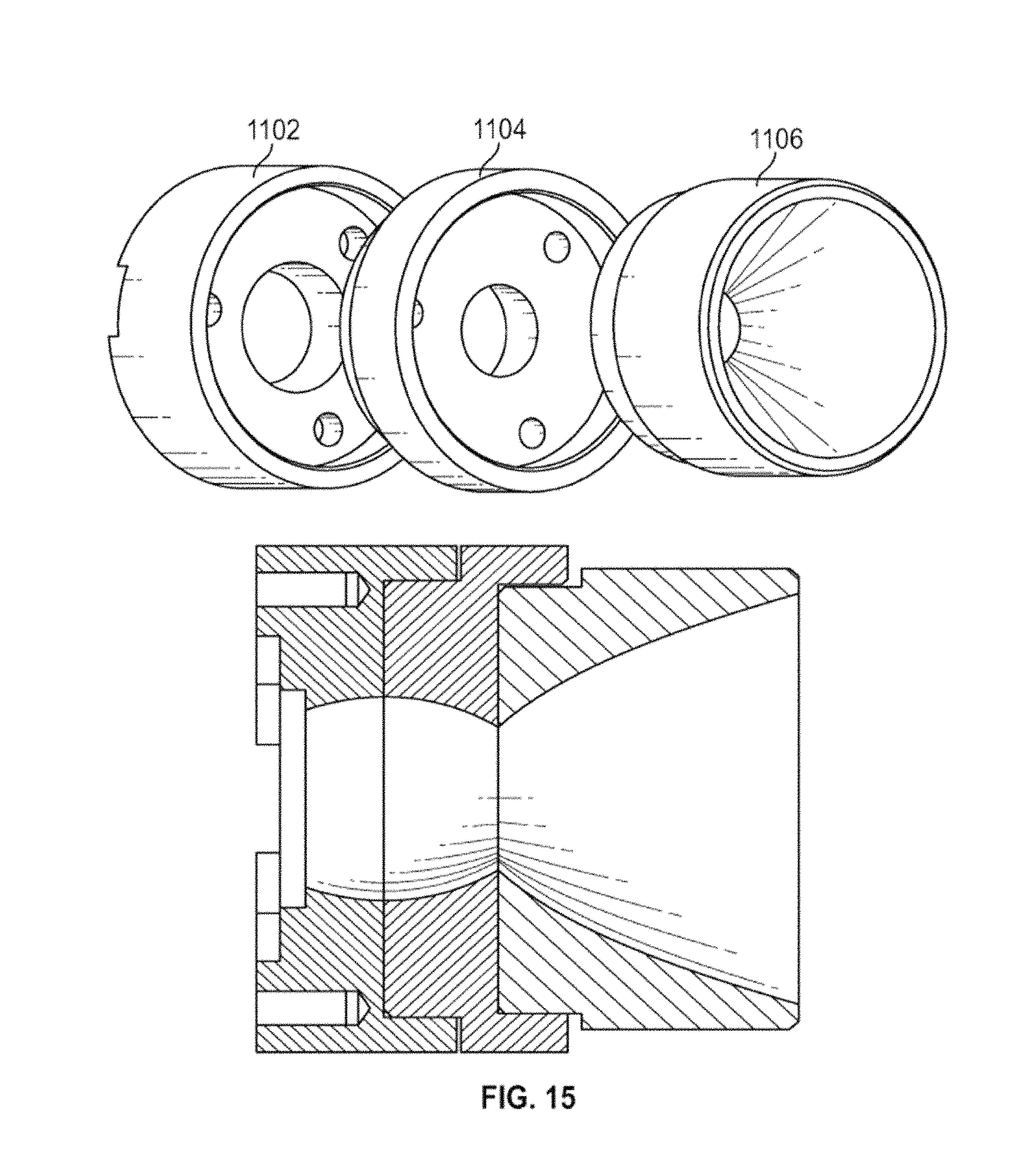
D00014

D00015

D00016

D00017
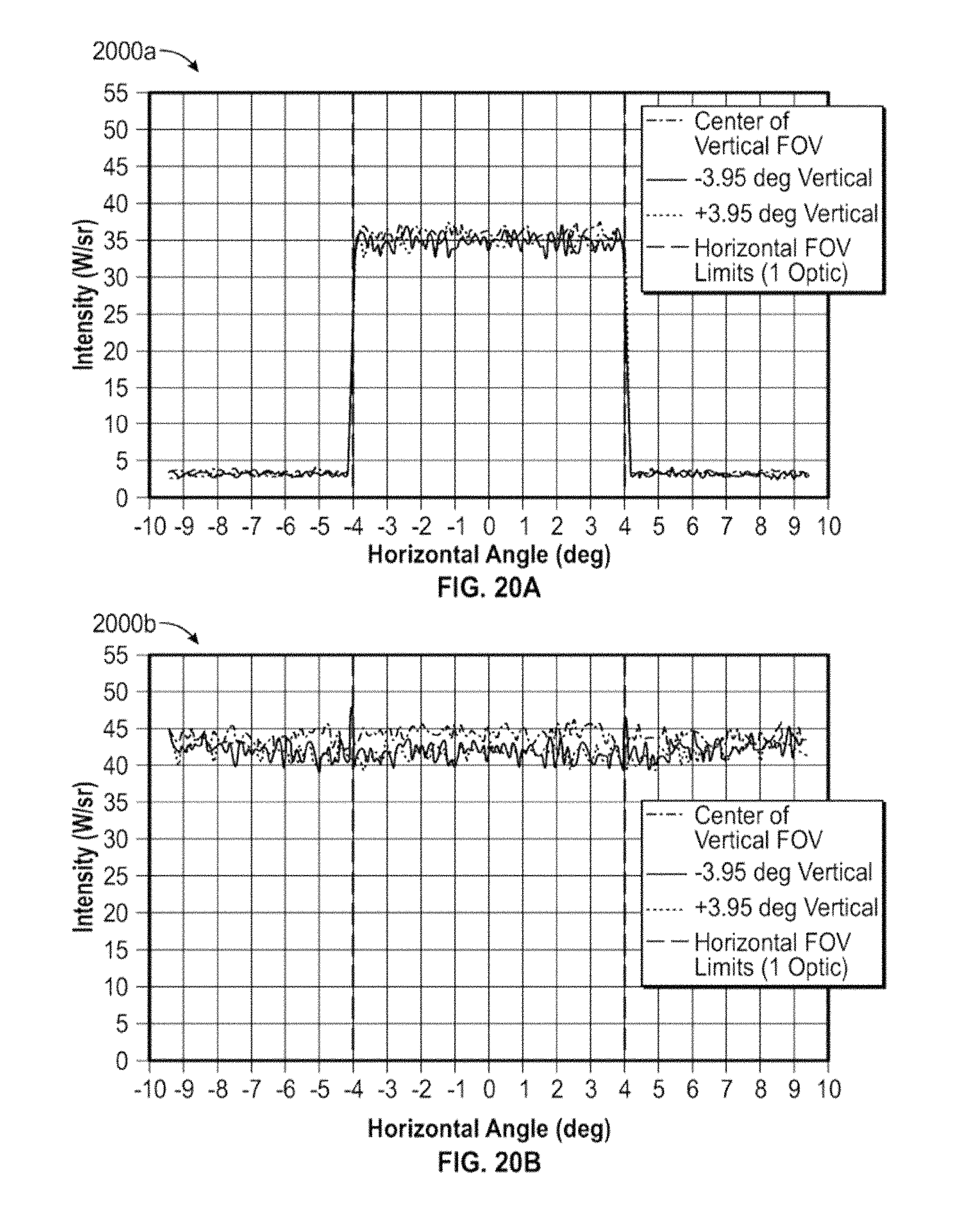
D00018

D00019
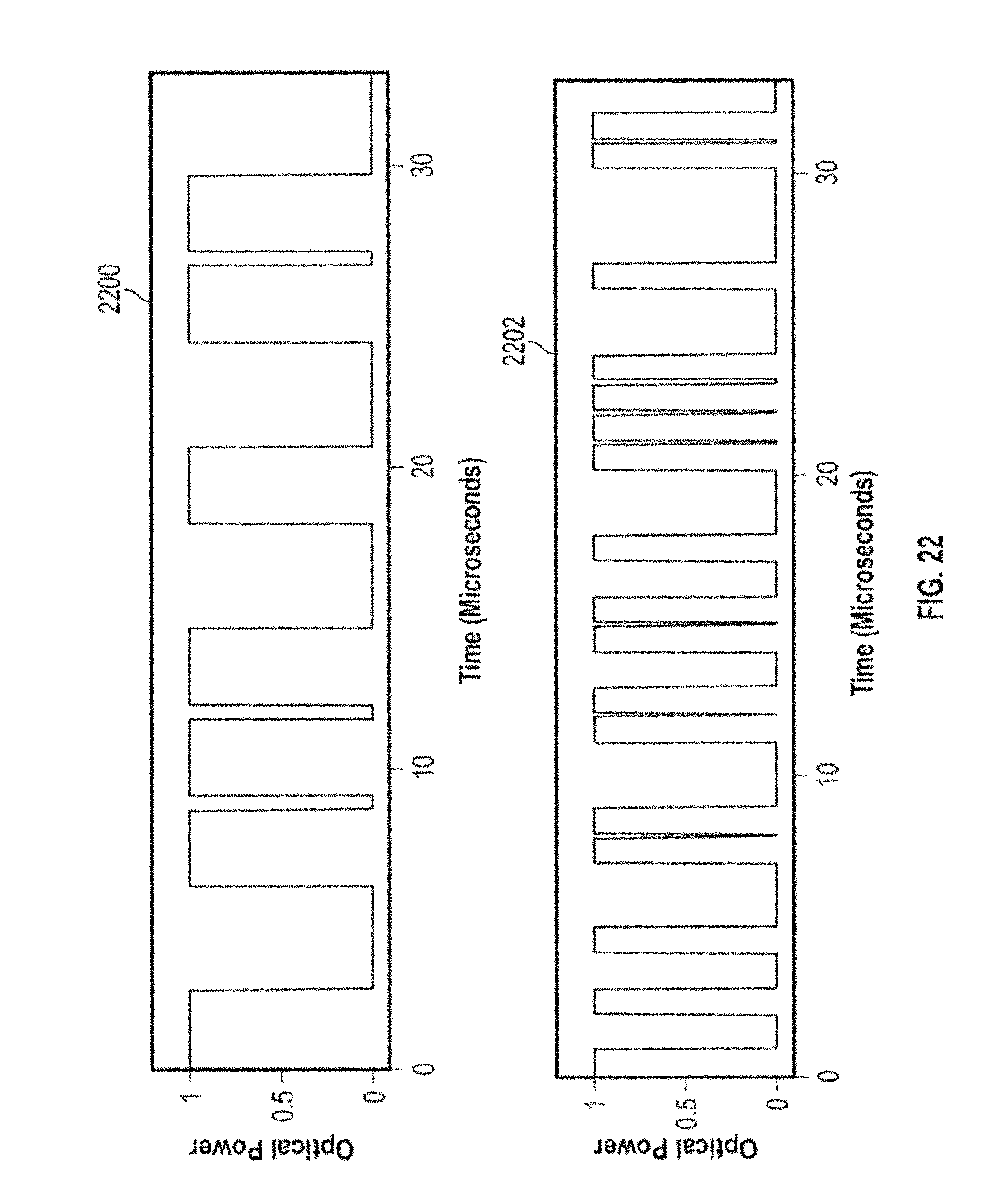
D00020
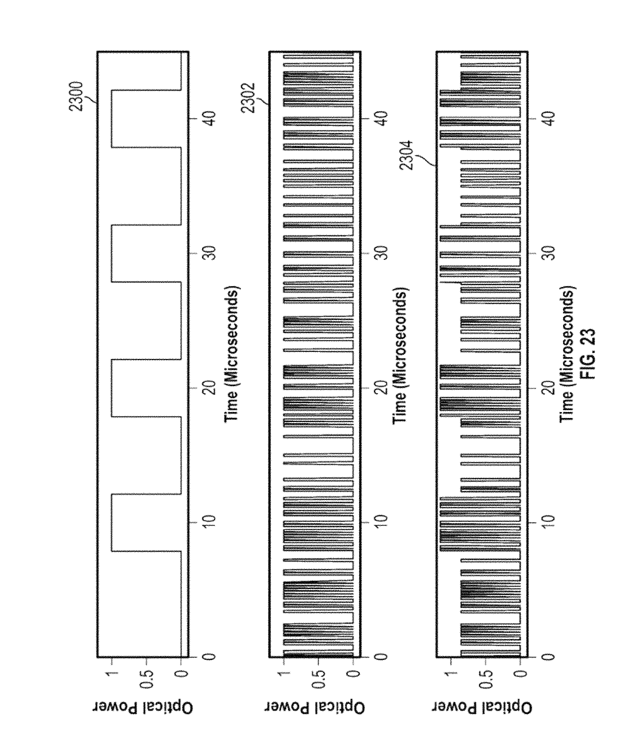
D00021

D00022
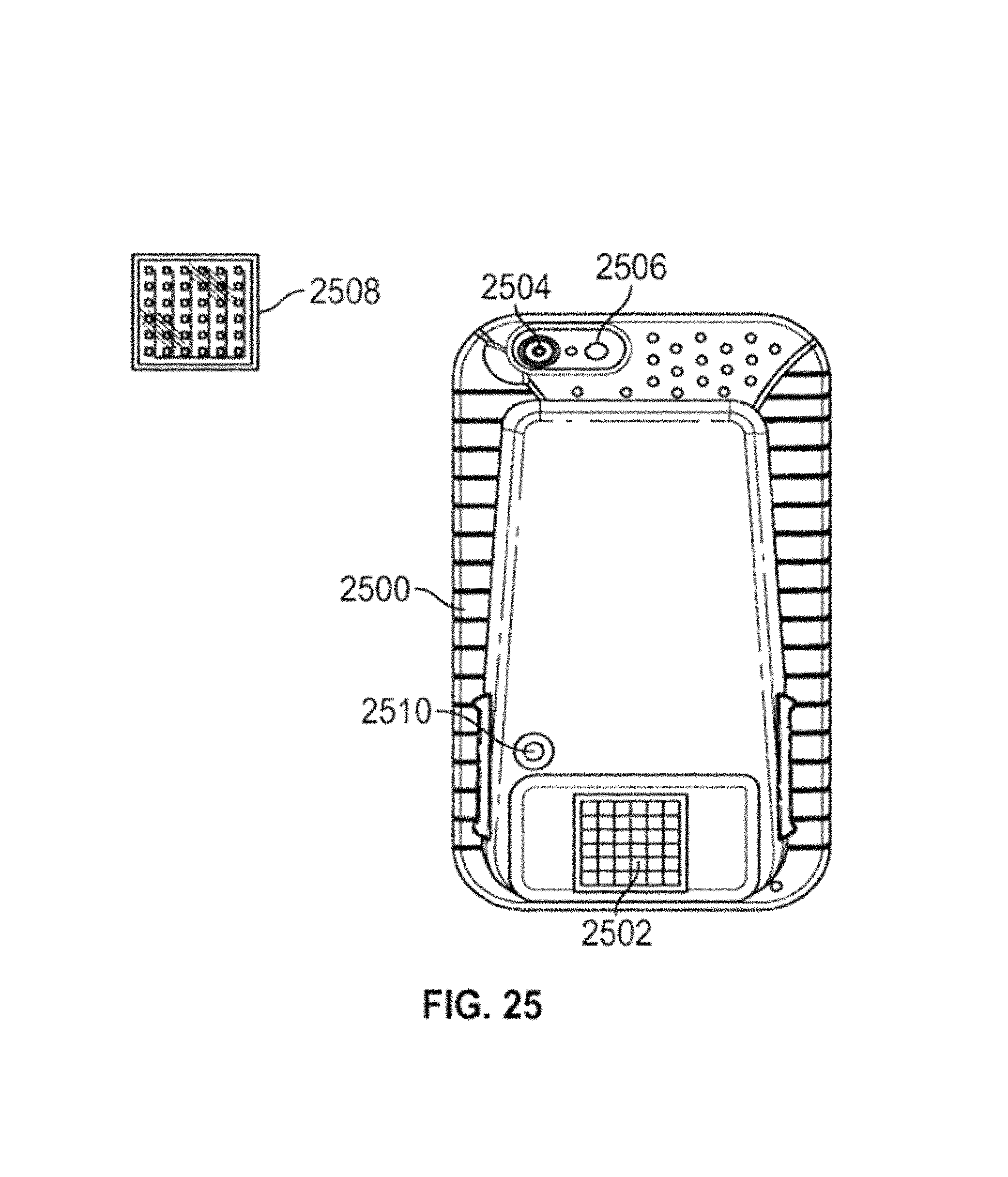
D00023
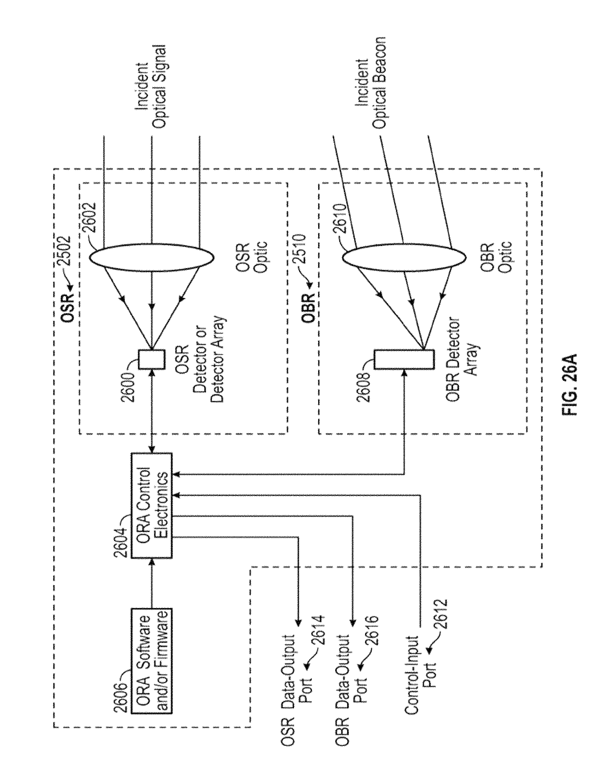
D00024
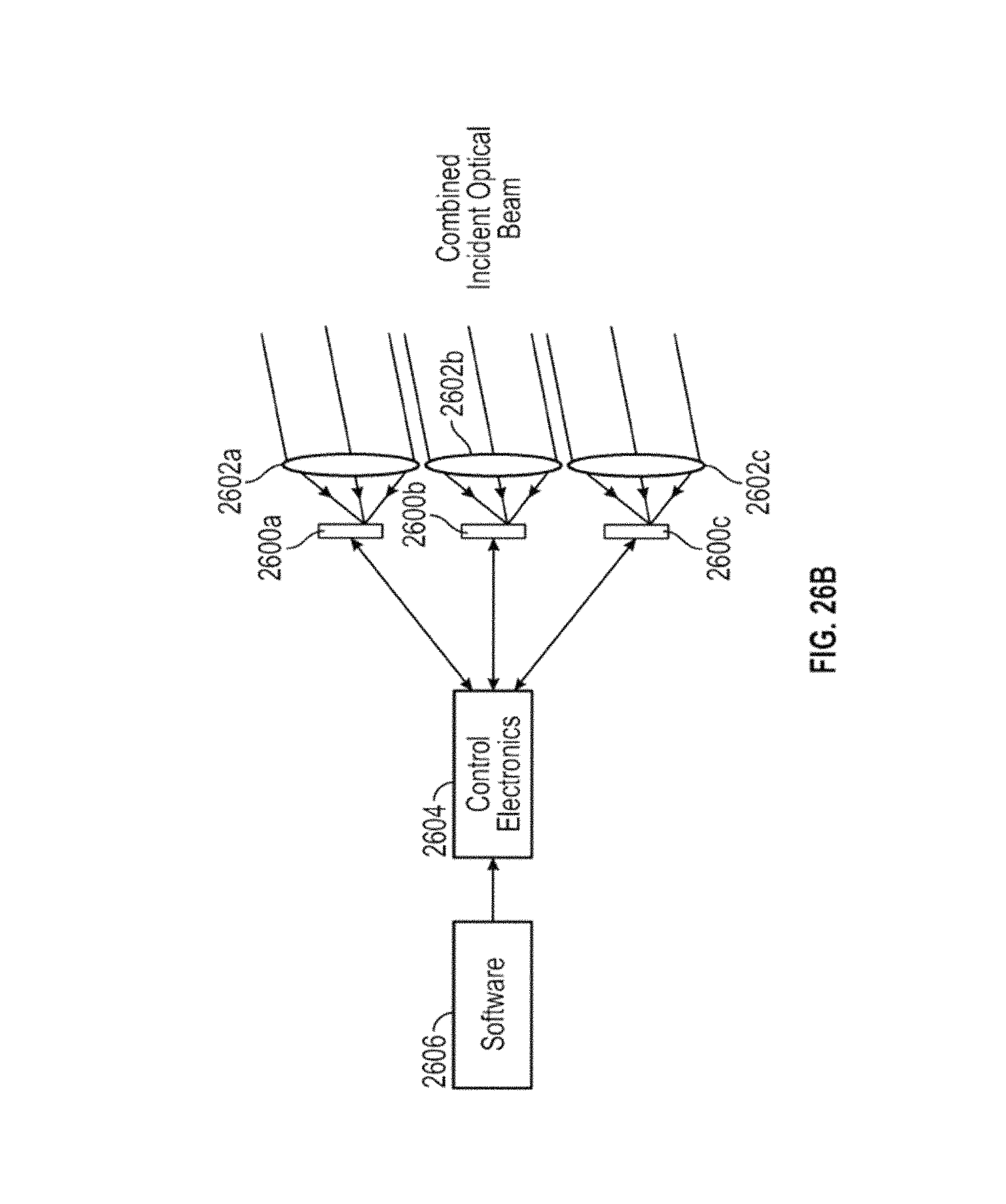
D00025
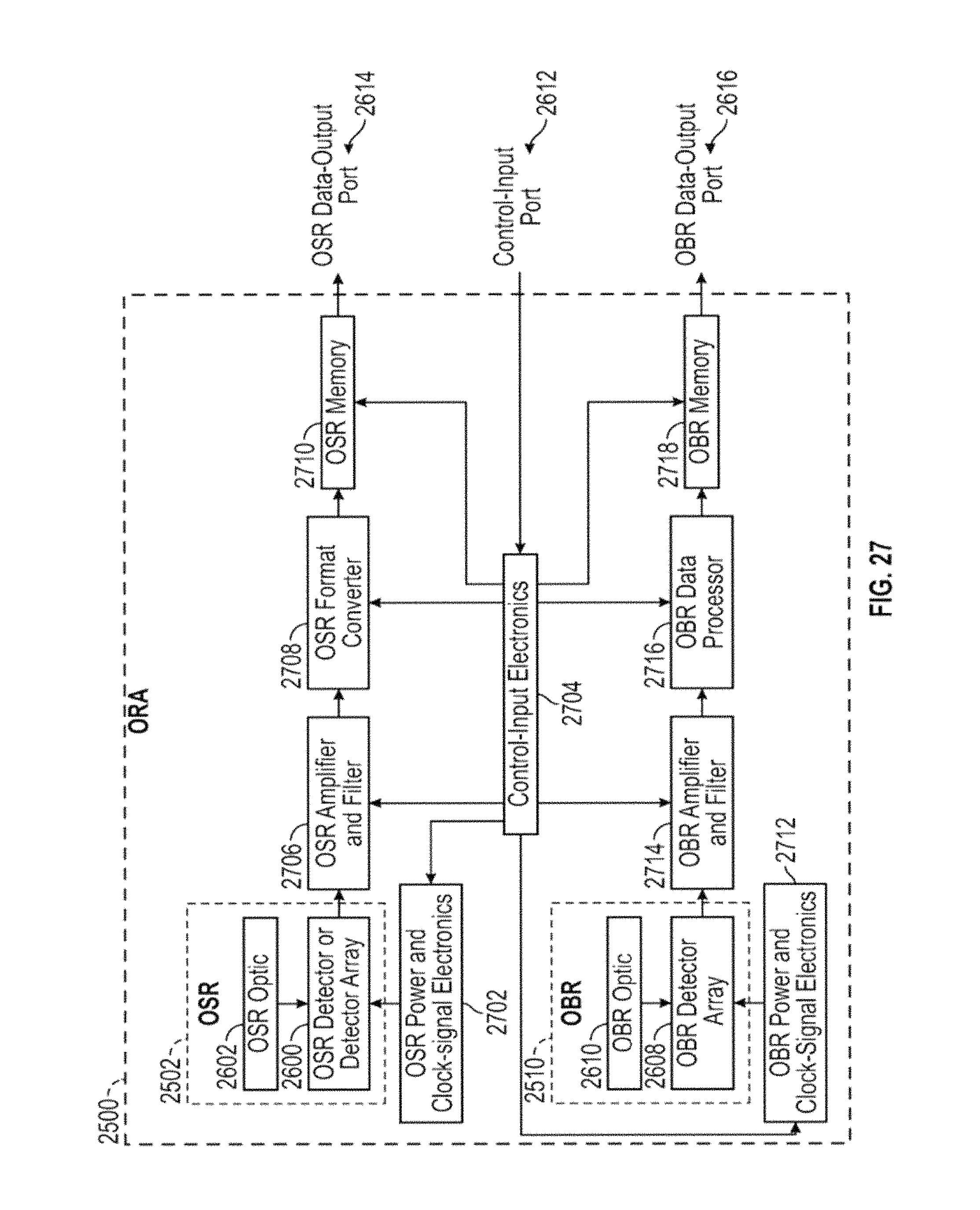
D00026
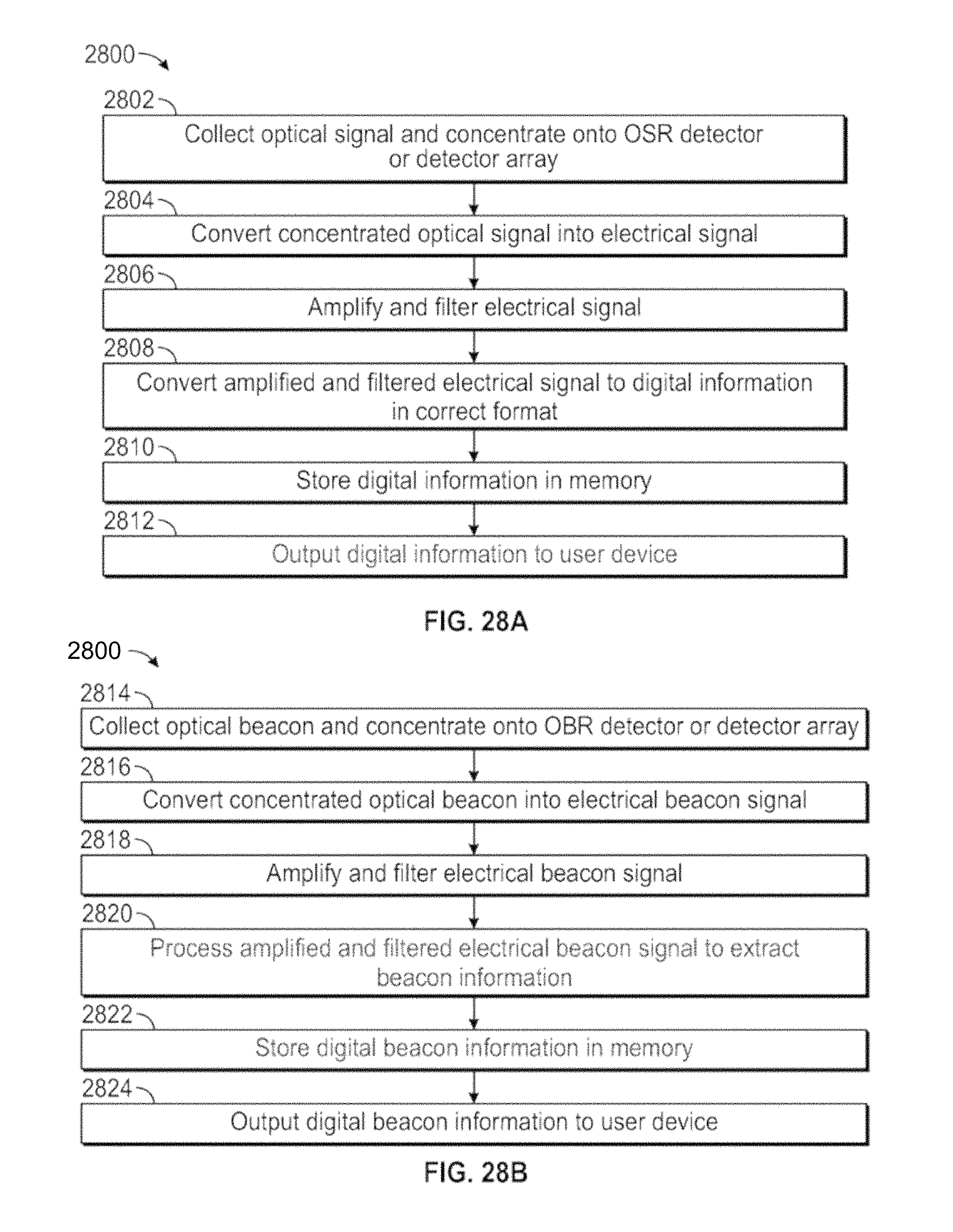
D00027

D00028
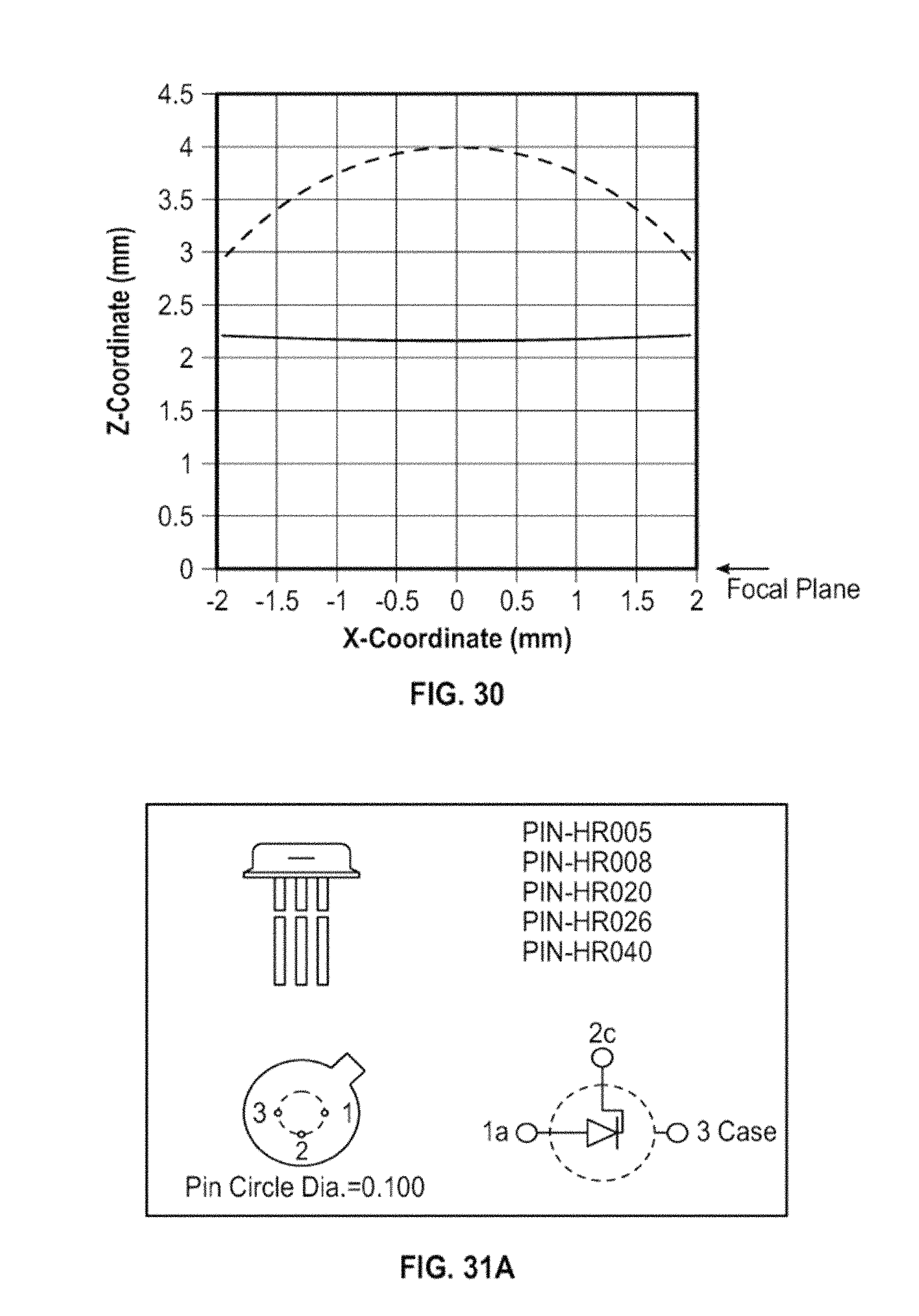
D00029
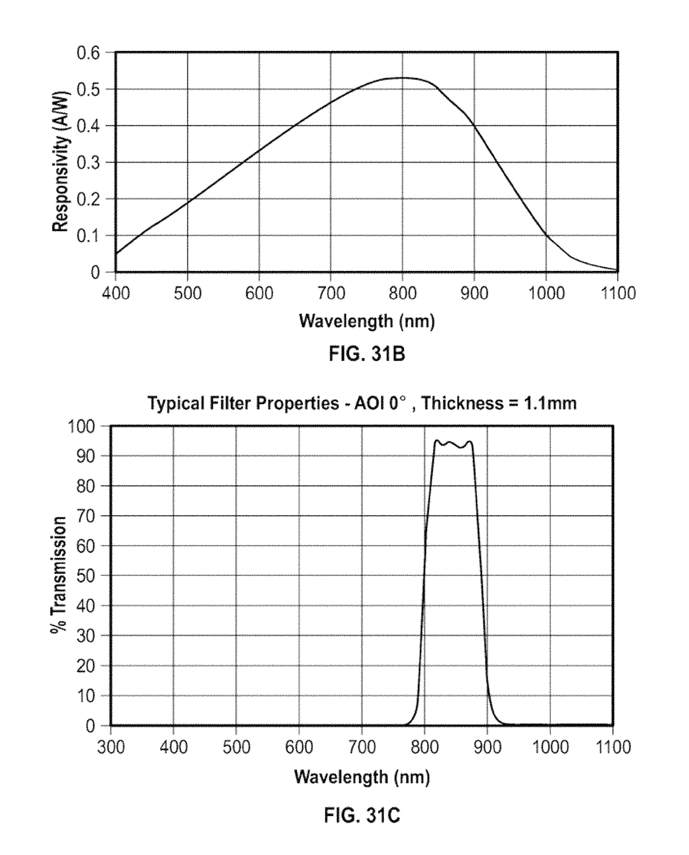
D00030

D00031
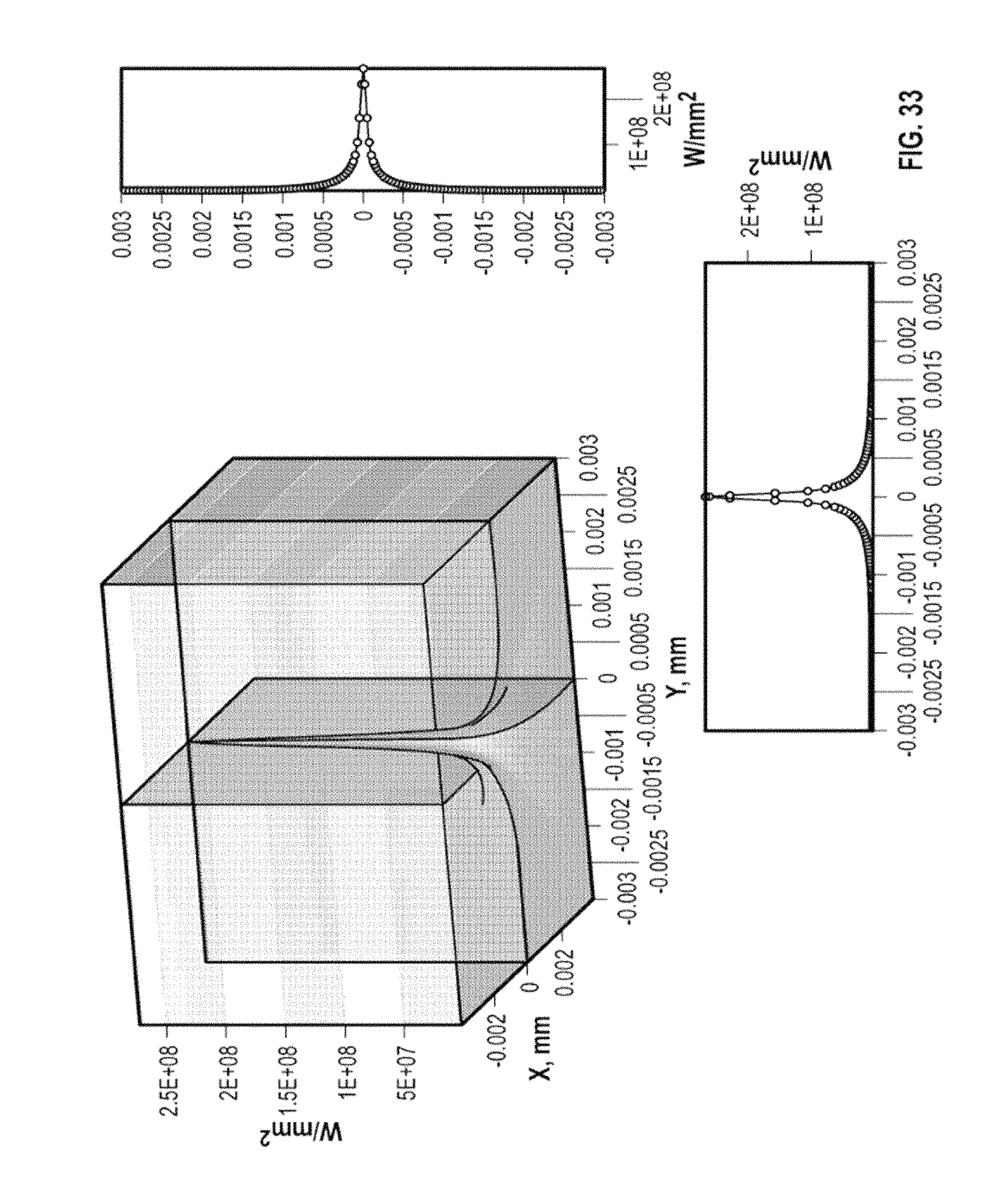
D00032

D00033

D00034

D00035

D00036
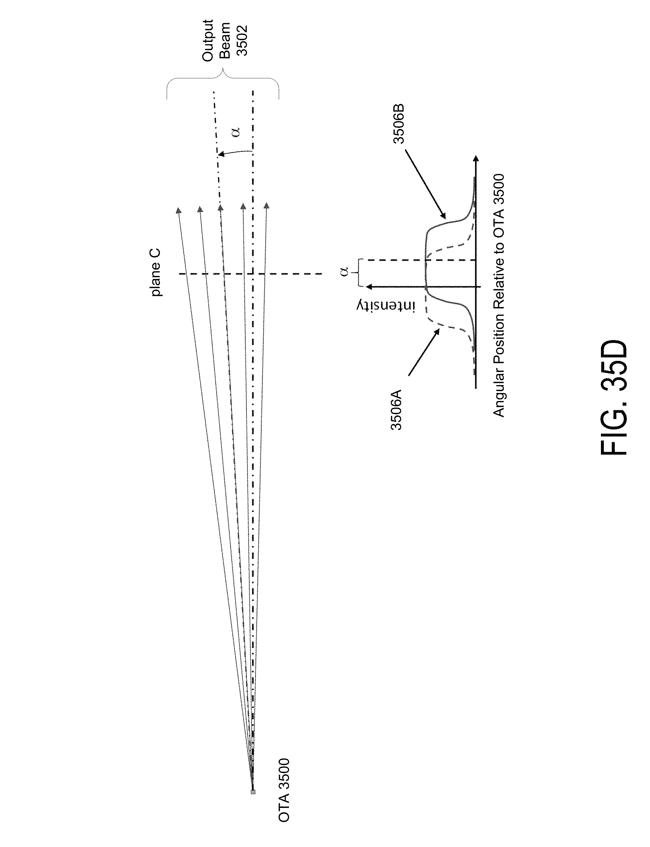
D00037
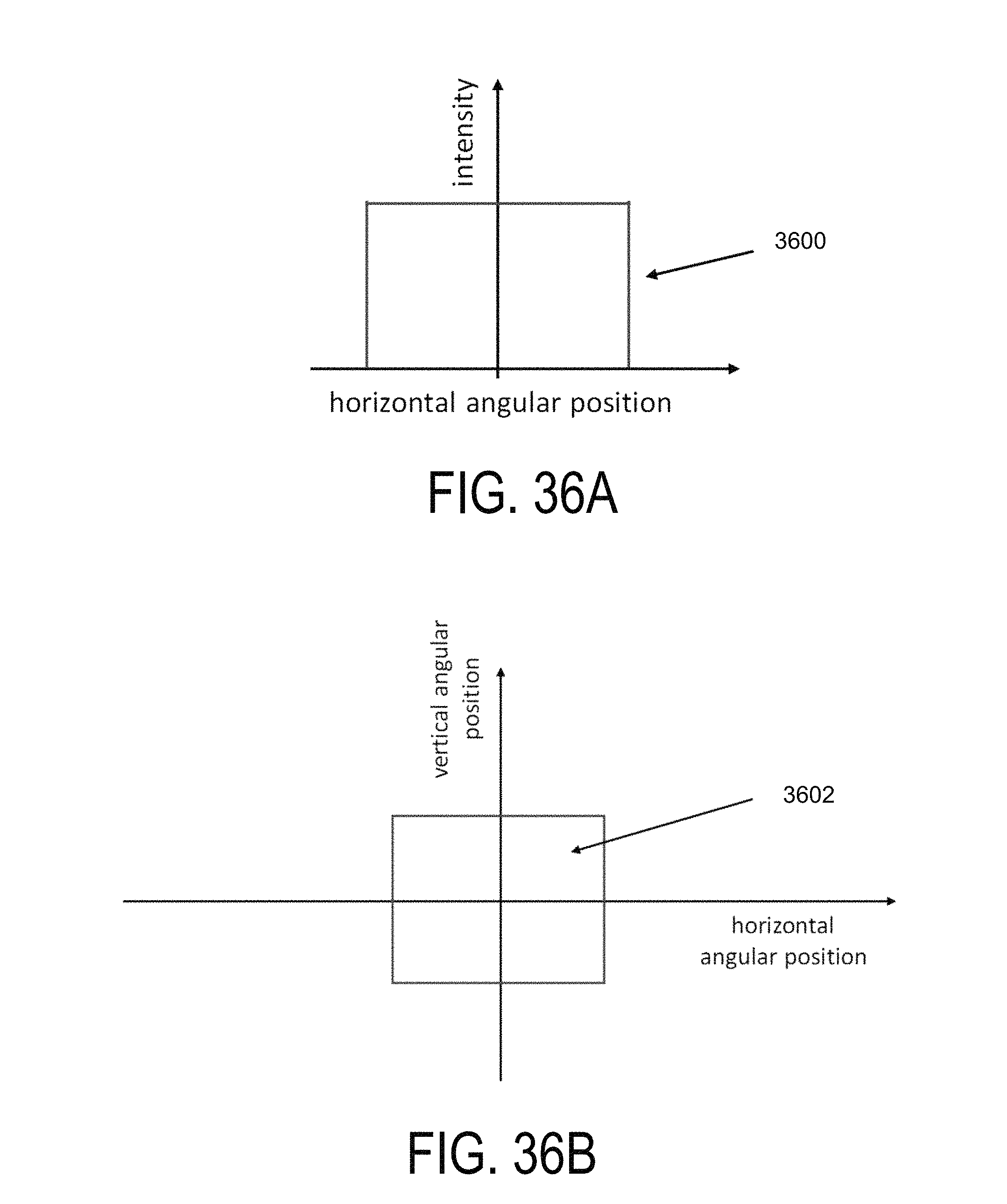
D00038
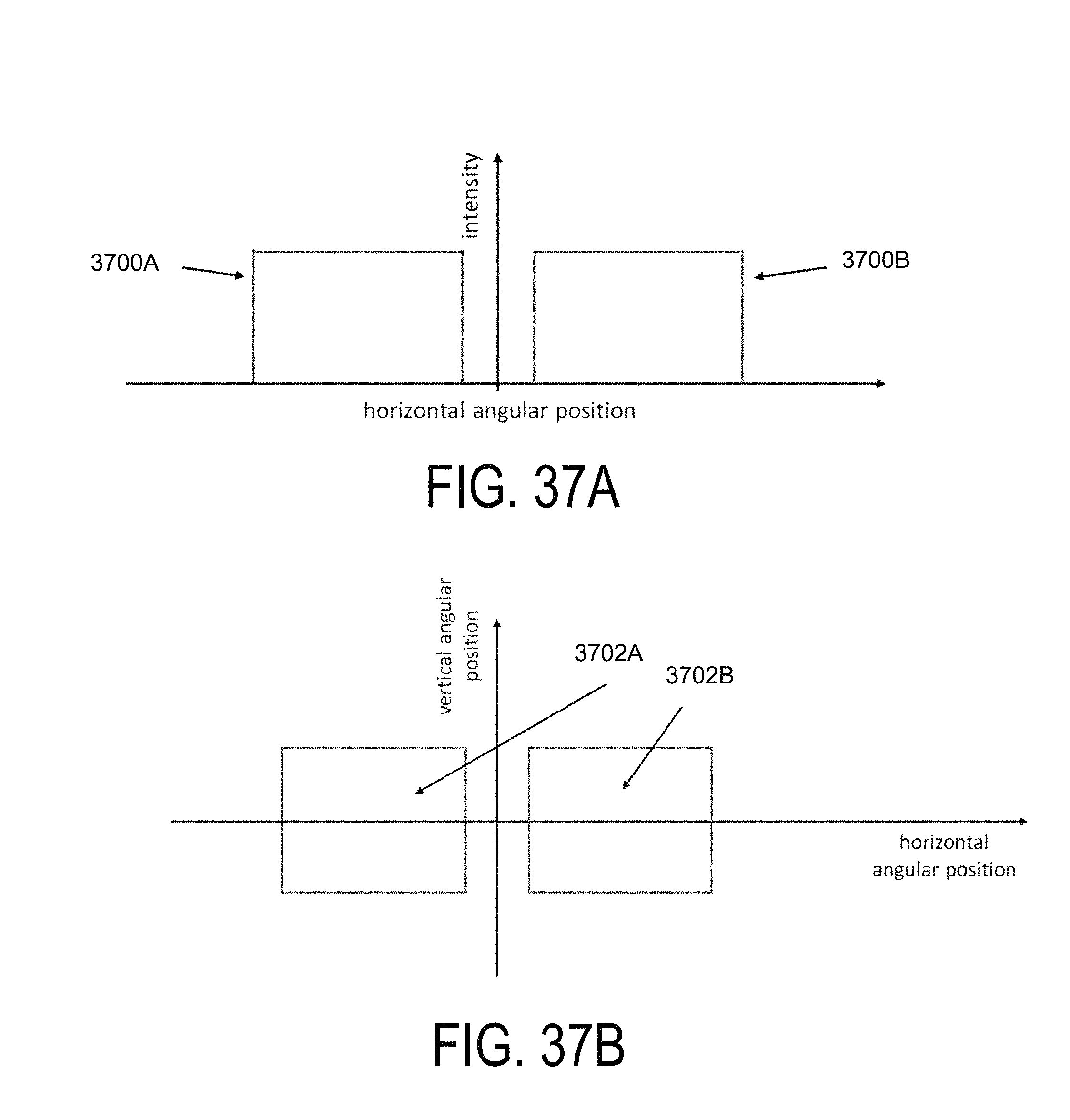
D00039

D00040

D00041
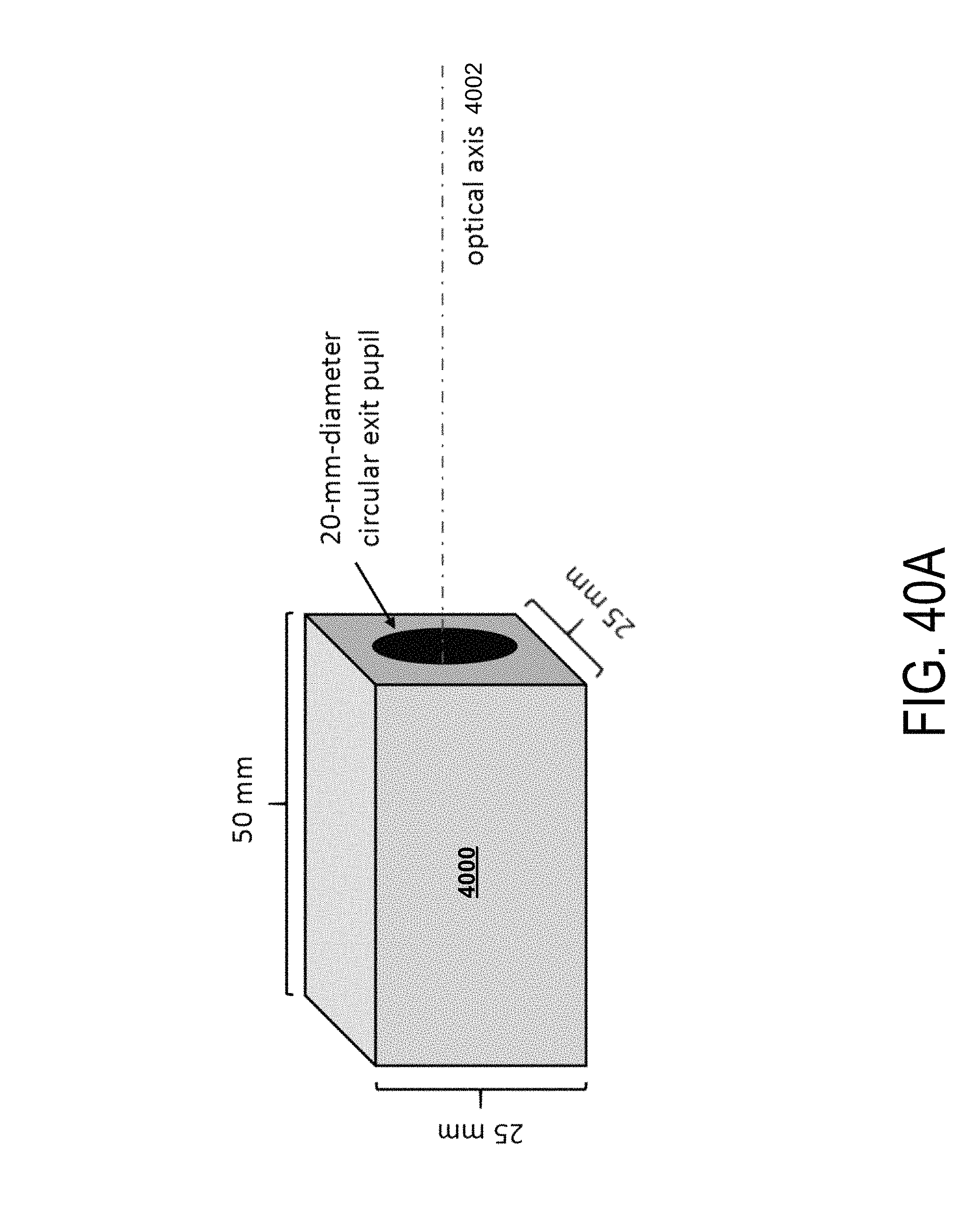
D00042
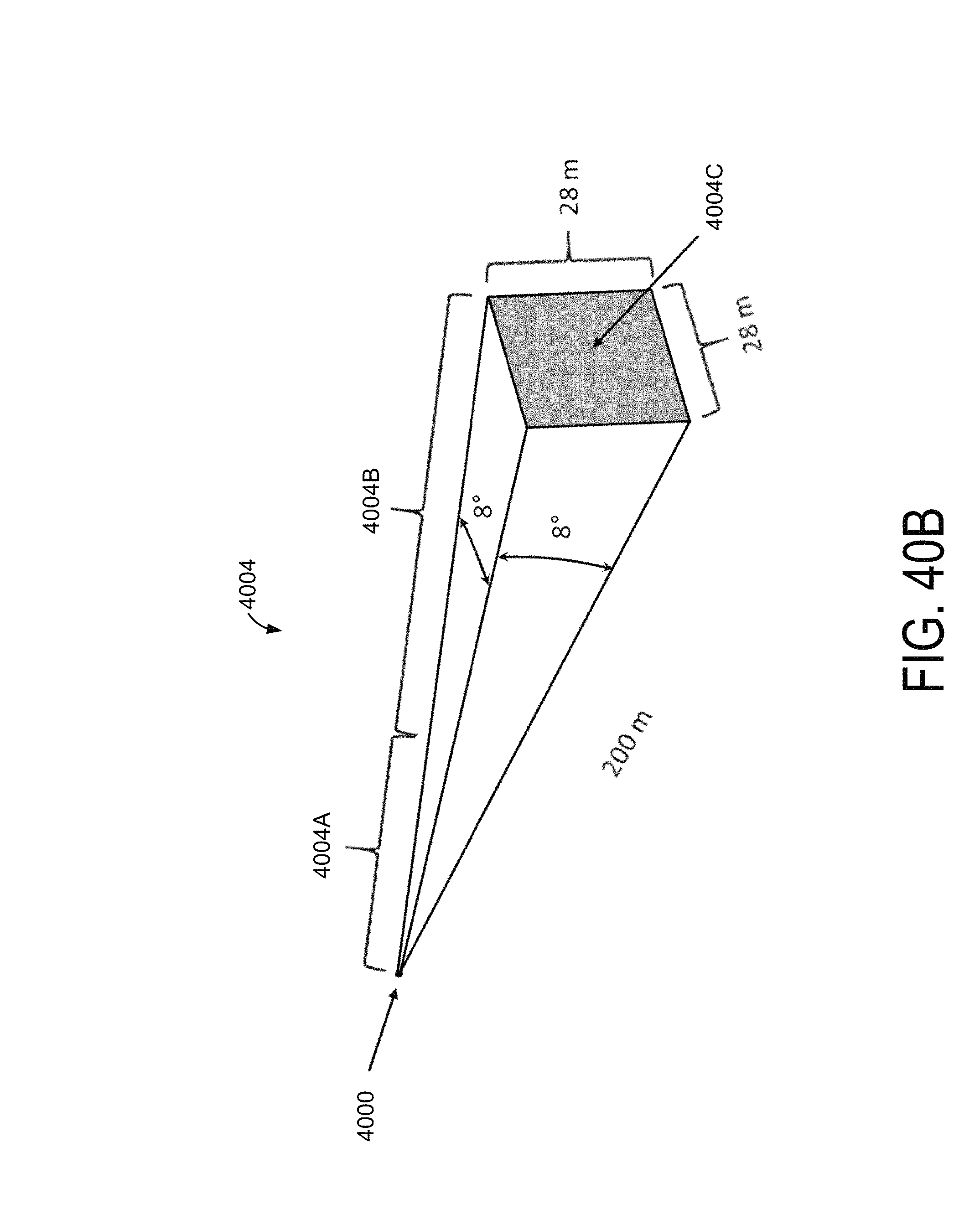
D00043
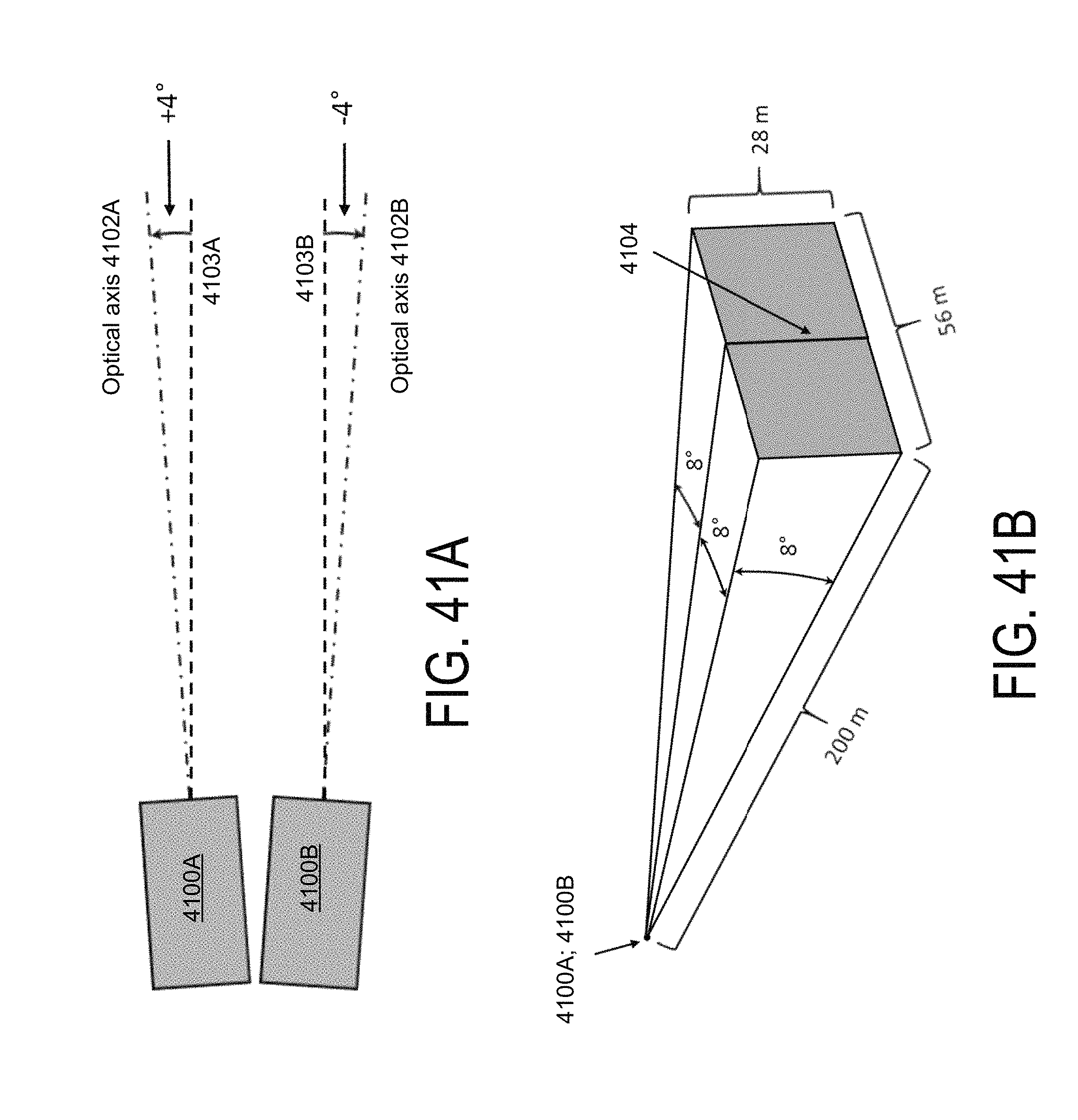
D00044
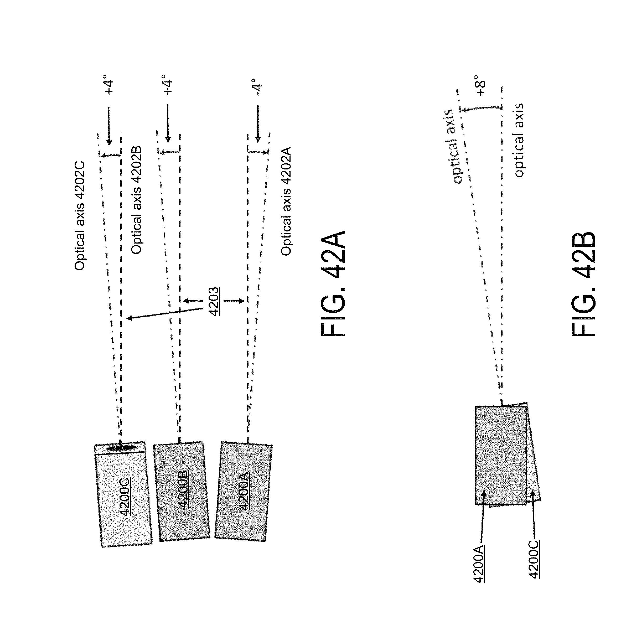
D00045
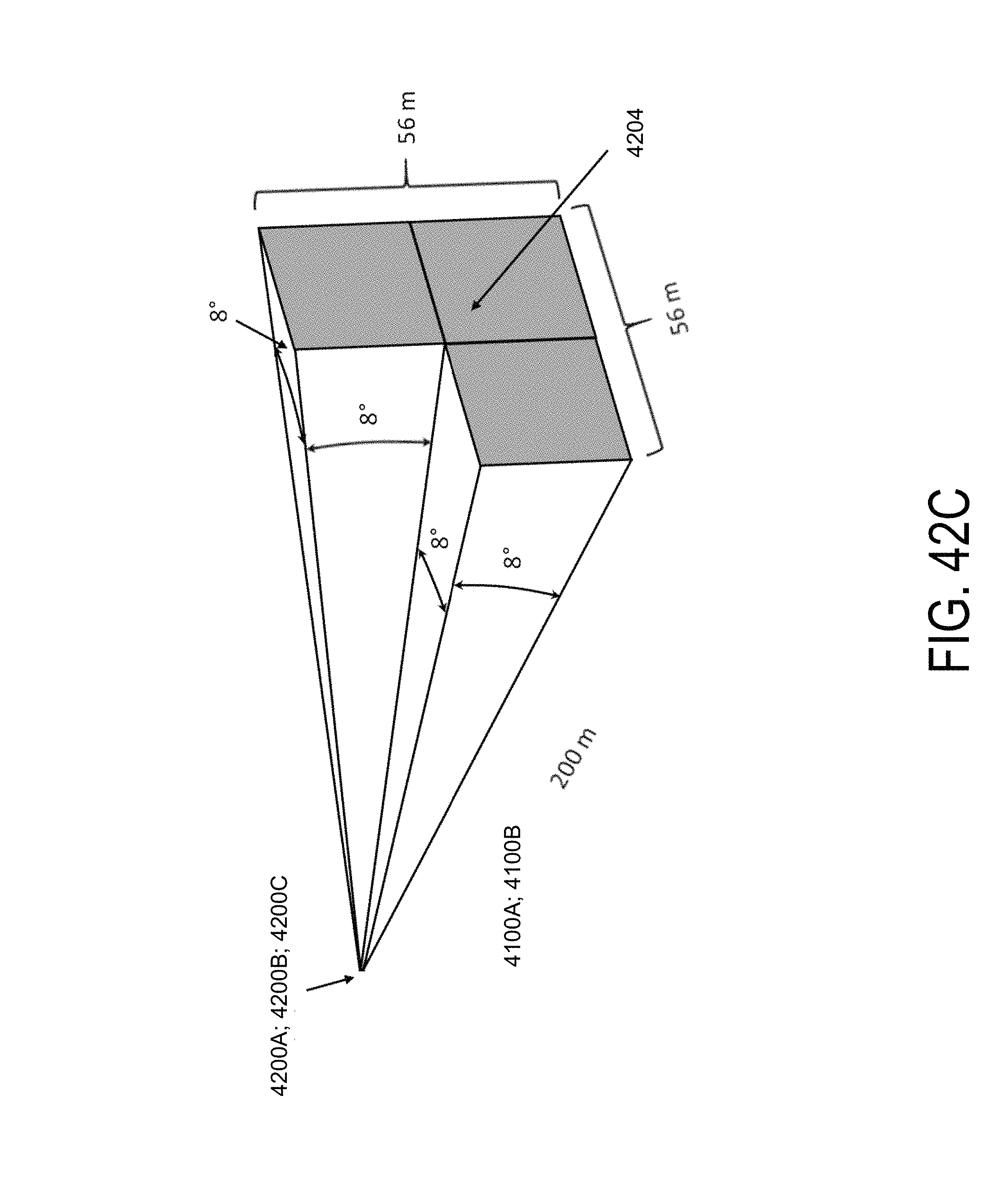
D00046
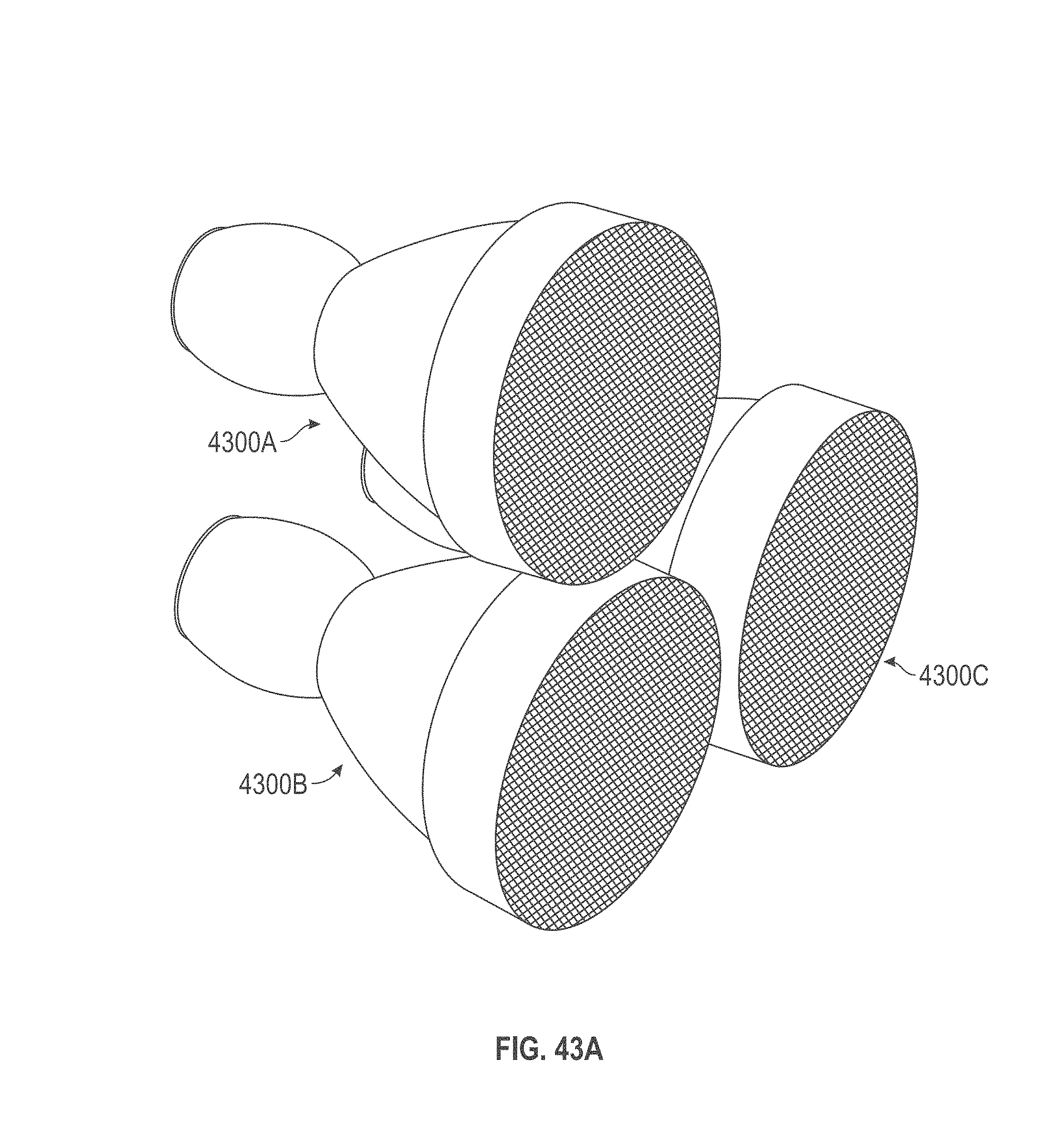
D00047
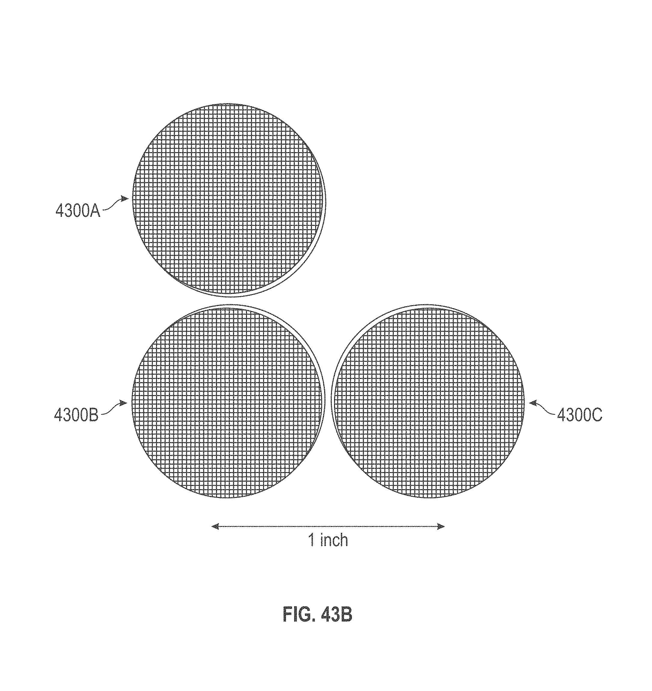
D00048
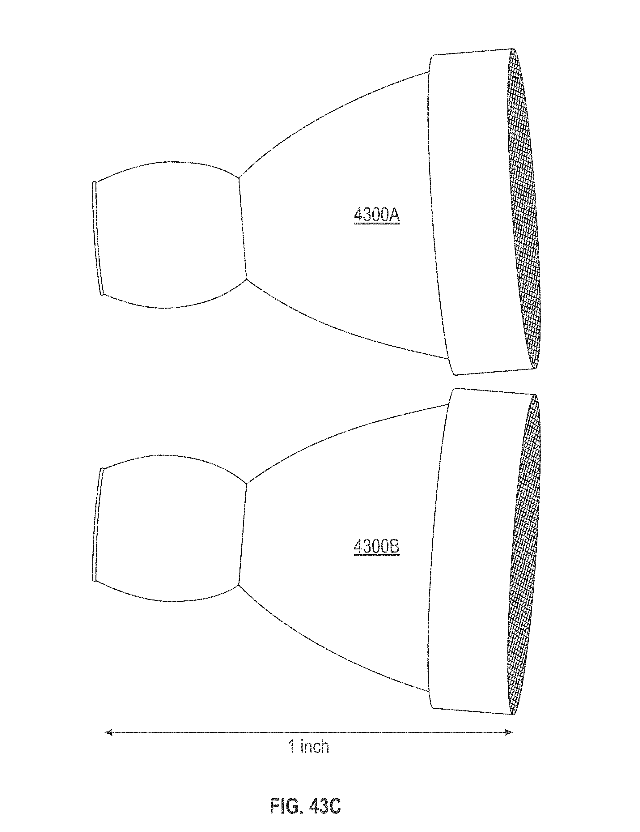
D00049
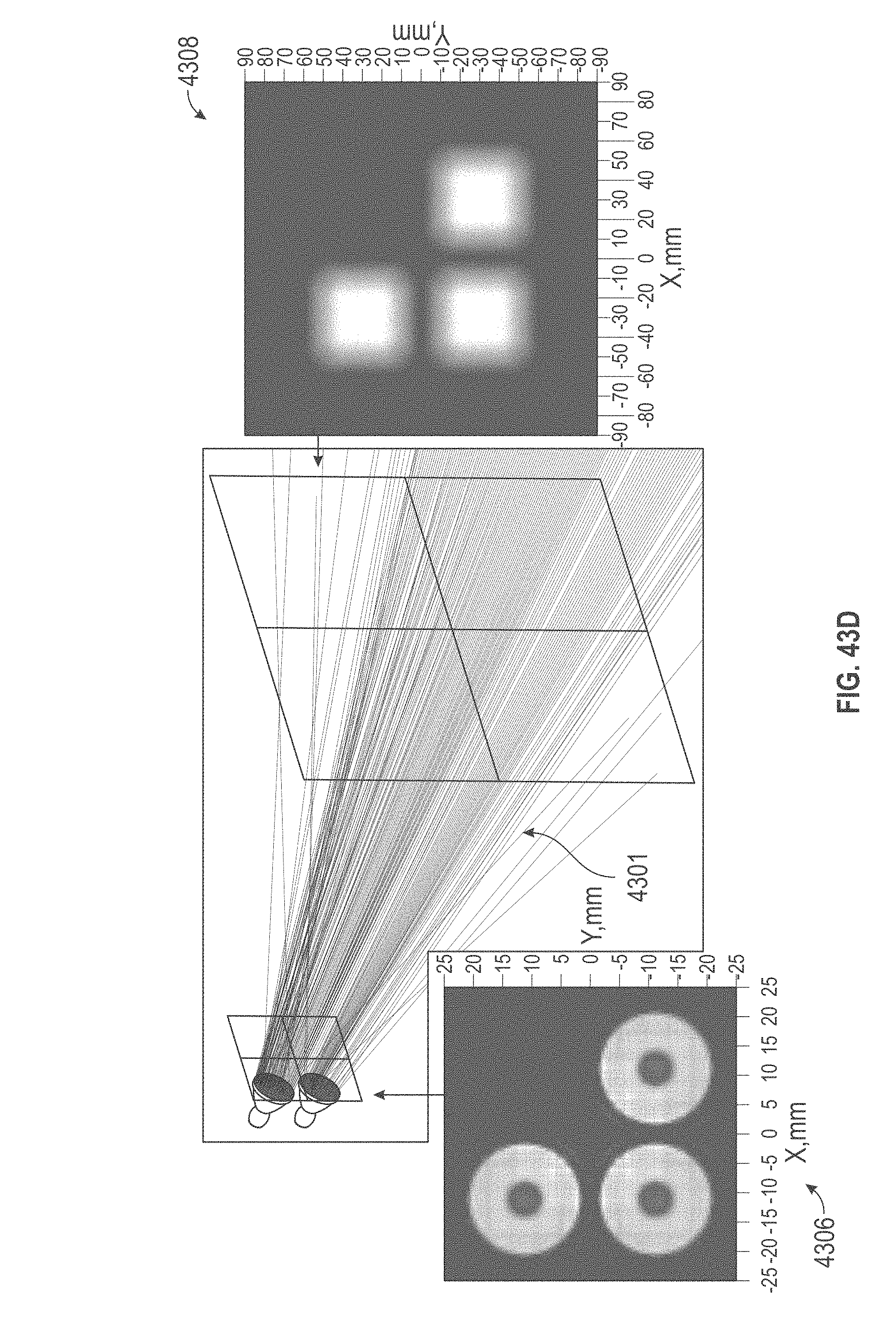
D00050
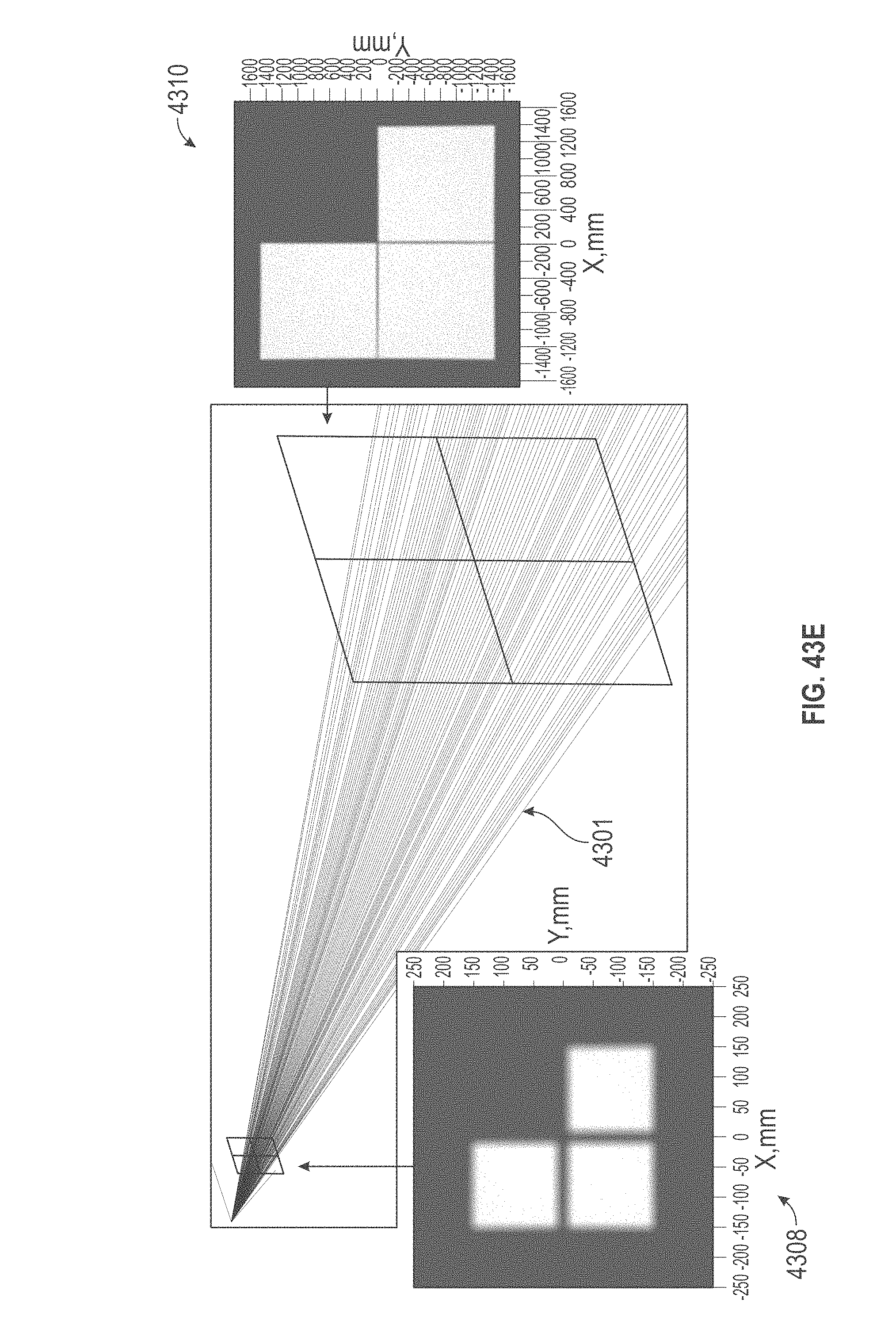
D00051
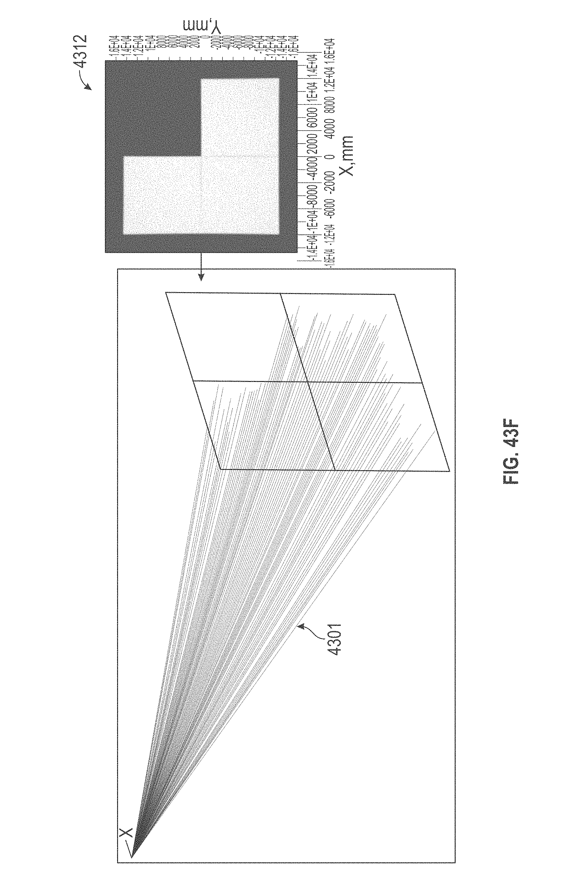
D00052

M00001

M00002

M00003

M00004

M00005

M00006

M00007

M00008

M00009

M00010

M00011

M00012

M00013

M00014

M00015

M00016

M00017

M00018

M00019

M00020

M00021

M00022

M00023

P00001

XML
uspto.report is an independent third-party trademark research tool that is not affiliated, endorsed, or sponsored by the United States Patent and Trademark Office (USPTO) or any other governmental organization. The information provided by uspto.report is based on publicly available data at the time of writing and is intended for informational purposes only.
While we strive to provide accurate and up-to-date information, we do not guarantee the accuracy, completeness, reliability, or suitability of the information displayed on this site. The use of this site is at your own risk. Any reliance you place on such information is therefore strictly at your own risk.
All official trademark data, including owner information, should be verified by visiting the official USPTO website at www.uspto.gov. This site is not intended to replace professional legal advice and should not be used as a substitute for consulting with a legal professional who is knowledgeable about trademark law.