Variable space mandrel cut for self aligned double patterning
Shu , et al. Fe
U.S. patent number 10,199,265 [Application Number 15/430,039] was granted by the patent office on 2019-02-05 for variable space mandrel cut for self aligned double patterning. This patent grant is currently assigned to GLOBALFOUNDRIES INC.. The grantee listed for this patent is GLOBALFOUNDRIES INC.. Invention is credited to Byoung Youp Kim, Jinping Liu, Jiehui Shu.


| United States Patent | 10,199,265 |
| Shu , et al. | February 5, 2019 |
Variable space mandrel cut for self aligned double patterning
Abstract
The present disclosure relates to semiconductor structures and, more particularly, to variable space mandrel cut for self-aligned double patterning and methods of manufacture. The method includes: forming a plurality of mandrels on a substrate; forming spacers about the plurality of mandrels and exposed portions of the substrate; removing a portion of at least one of the plurality of mandrels to form an opening; and filling in the opening with material.
| Inventors: | Shu; Jiehui (Clifton Park, NY), Kim; Byoung Youp (Schenectady, NY), Liu; Jinping (Ballston Lake, NY) | ||||||||||
|---|---|---|---|---|---|---|---|---|---|---|---|
| Applicant: |
|
||||||||||
| Assignee: | GLOBALFOUNDRIES INC. (Grand
Cayman, KY) |
||||||||||
| Family ID: | 63105897 | ||||||||||
| Appl. No.: | 15/430,039 | ||||||||||
| Filed: | February 10, 2017 |
Prior Publication Data
| Document Identifier | Publication Date | |
|---|---|---|
| US 20180233404 A1 | Aug 16, 2018 | |
| Current U.S. Class: | 1/1 |
| Current CPC Class: | H01L 21/76825 (20130101); H01L 21/76802 (20130101); H01L 23/5329 (20130101); H01L 21/76831 (20130101); H01L 23/528 (20130101); H01L 21/0337 (20130101); H01L 21/76816 (20130101); H01L 23/5226 (20130101); H01L 21/31144 (20130101) |
| Current International Class: | H01L 21/768 (20060101); H01L 23/522 (20060101); H01L 23/528 (20060101); H01L 23/532 (20060101) |
| Field of Search: | ;257/622,66,72,223,227,291,292,439,443,655,E27.1,E27.125,E27.112,E29.117,E29.145,E29.147,E29.151,E29.182,E29.202,E29.273-E29.299,E29.314,E29.32,E23.016 ;438/149 |
References Cited [Referenced By]
U.S. Patent Documents
| 9177797 | November 2015 | Chang et al. |
| 9299787 | March 2016 | Cheng |
| 2007/0287255 | December 2007 | Doyle |
| 2013/0119474 | May 2013 | Schultz |
| 2014/0097499 | April 2014 | Parekh et al. |
| 2015/0147886 | May 2015 | Tung |
| 2016/0013185 | January 2016 | Greene |
| 2016/0093720 | March 2016 | Chudzik |
| 102224569 | Oct 2011 | CN | |||
| 201515116 | Apr 2015 | TW | |||
Other References
|
Examination Report for related TW Application No. 106114622 dated Feb. 9, 2018, 9 pages. cited by applicant . Notice of Allowance for related TW Application No. 106114622 dated Jun. 26, 2018, 4 pages. cited by applicant. |
Primary Examiner: Nguyen; Tram H
Attorney, Agent or Firm: Canale; Anthony Calderon; Andrew M. Roberts Mlotkowski Safran Cole & Calderon, P.C.
Claims
What is claimed:
1. A method, comprising: forming a plurality of mandrels on a substrate; depositing spacer material on the plurality of mandrels and the substrate between the mandrels; forming spacers about the plurality of mandrels by etching back the spacer material to expose a surface of the plurality of mandrels and a surface of the substrate between the spacers on the plurality of mandrels; removing a portion of at least one of the plurality of mandrels to form an opening; filling the opening with material; forming a coating on the exposed surface of the plurality of mandrels and the exposed surface of the substrate, between the spacers; and etching back the coating to expose top surfaces of the plurality of mandrels, wherein the material filling the opening and the spacers are of a same material.
2. The method of claim 1, wherein the same material is TiO.sub.x.
3. The method of claim 1, wherein: a spacing between the spacers is approximately a dimension equal to a thickness of a mandrel of the plurality of mandrels; and a thickness of the mandrel of the plurality of mandrels is substantially the same as a thickness of a spacer of the spacers.
4. The method of claim 1, wherein the coating is a spin on glass material.
5. The method of claim 4, wherein the coating is SiO.sub.2 or SiOC.
6. The method of claim 1, further comprising: forming a photolithographic stack of material on the coating; forming a mask opening in the photolithographic stack of material in alignment with a portion of at least one of the plurality of mandrels; and removing a portion of the at least one mandrel to form a cut along a length thereof by etching an exposed portion of the at least one mandrel through the mask opening.
7. The method of claim 6, wherein the cut is greater than 2.times. the width of the spacers.
8. The method of claim 7, wherein the material filling the cut is TiO.sub.x and the spacers are TiO.sub.x.
9. A method comprises: forming a plurality of mandrels on a substrate; depositing spacer material on the plurality of mandrels and the substrate between the mandrels; forming spacers on the plurality of mandrels by etching back the spacer material of the spacers which exposes a top surface of the plurality of mandrels and portions of the substrate; forming a coating on the exposed surface of the substrate and on the spacers; removing a portion of at least one of the plurality of mandrels to form a cut along a length thereof; and filling the cut with material, wherein the cut is formed by applying a photoresist mask on the plurality of mandrels, the coating and the spacers, followed by forming a mask opening in the photoresist mask, and an etching of the portion of the at least one of the plurality of mandrels.
10. The method of claim 9, wherein the material and the spacers are both TiO.sub.x.
11. The method of claim 9, wherein the coating is a spin on glass material.
12. The method of claim 9, further comprising removing the coating after filling of the cut.
13. The method of claim 9, wherein the cut is greater than 2.times. a spacer thickness.
14. The method of claim 13, wherein the plurality of mandrels is a different material than the coating and the spacers.
15. The method of claim 14, wherein remaining of the plurality of mandrels are protected by the photoresist mask when the cut is formed in the portion of the at least one of the plurality of mandrels.
16. A structure, comprising: a plurality of mandrels; spacers comprising a spacer material on sidewalls of the plurality of mandrels; at least one of the plurality of mandrels having a cut along a length thereof; another spacer material filling the cut along the length thereof; and a spacing between the spacers is approximately a dimension equal to a thickness of a mandrel of the plurality of mandrels, wherein the thickness of the mandrel of the plurality of mandrels is substantially the same as a thickness of a spacer of the spacers.
Description
FIELD OF THE INVENTION
The present disclosure relates to semiconductor structures and, more particularly, to variable space mandrel cut for self-aligned double patterning and methods of manufacture.
BACKGROUND
As semiconductor processes continue to scale downwards, e.g., shrink, the desired spacing between elements (i.e., the pitch) of a device is less than the pitch that can be manufactured using traditional optical masks and photolithography equipment. One approach used to achieve higher resolution in smaller nodes, e.g., 20 nm or smaller devices, is to use multiple pattern lithography. For example, sidewall imaging techniques have been used to scale the spaces and features of a device. For example, in sidewall imaging techniques, dummy lines (e.g., at a minimum available pitch) are first formed, followed by formation of sidewall aligned spacers on the dummy lines. The dummy lines are removed while leaving the spacers, and then the spacers are used as patterning masks to transfer the desired pattern to underlying layers. In this way, line spacing at approximately half the minimum pitch can be achieved.
The use of additional materials (e.g., reverse material layers) for additional lithography patterning and cutting may be performed on the spacers prior to the removal of the dummy lines. This additional patterning/cutting allows for greater variation and/or more complex patterns to be formed in semiconductors for back end of line (BEOL) processes with small pitches. However, traditional techniques for additional patterning/cutting rely on multiple steps, which increases manufacturing cost. Also, many of these techniques can increase the parasitic performance of the device.
SUMMARY
In an aspect of the disclosure, a method comprises: forming a plurality of mandrels on a substrate forming spacers about the plurality of mandrels and exposed portions of the substrate; removing a portion of at least one of the plurality of mandrels to form an opening; and filling in the opening with material.
In an aspect of the disclosure, a method comprises: forming a plurality of mandrels on a substrate; forming spacers on the plurality of mandrels; etching back the spacers to expose a top surface of the plurality of mandrels and portions of the substrate; forming a coating on the exposed surface of the substrate and on the spacers; removing a portion of at least one of the plurality of mandrels to form a cut along a length thereof; and filling the cut with material.
In an aspect of the disclosure, a structure comprises: a plurality of mandrels; spacer material on sidewalls of the plurality of mandrels having a spacer material thereabout; at least one of the plurality of mandrels having a cut along a length thereof; and spacer material filling the cut along the length thereof.
BRIEF DESCRIPTION OF THE DRAWINGS
The present disclosure is described in the detailed description which follows, in reference to the noted plurality of drawings by way of non-limiting examples of exemplary embodiments of the present disclosure.
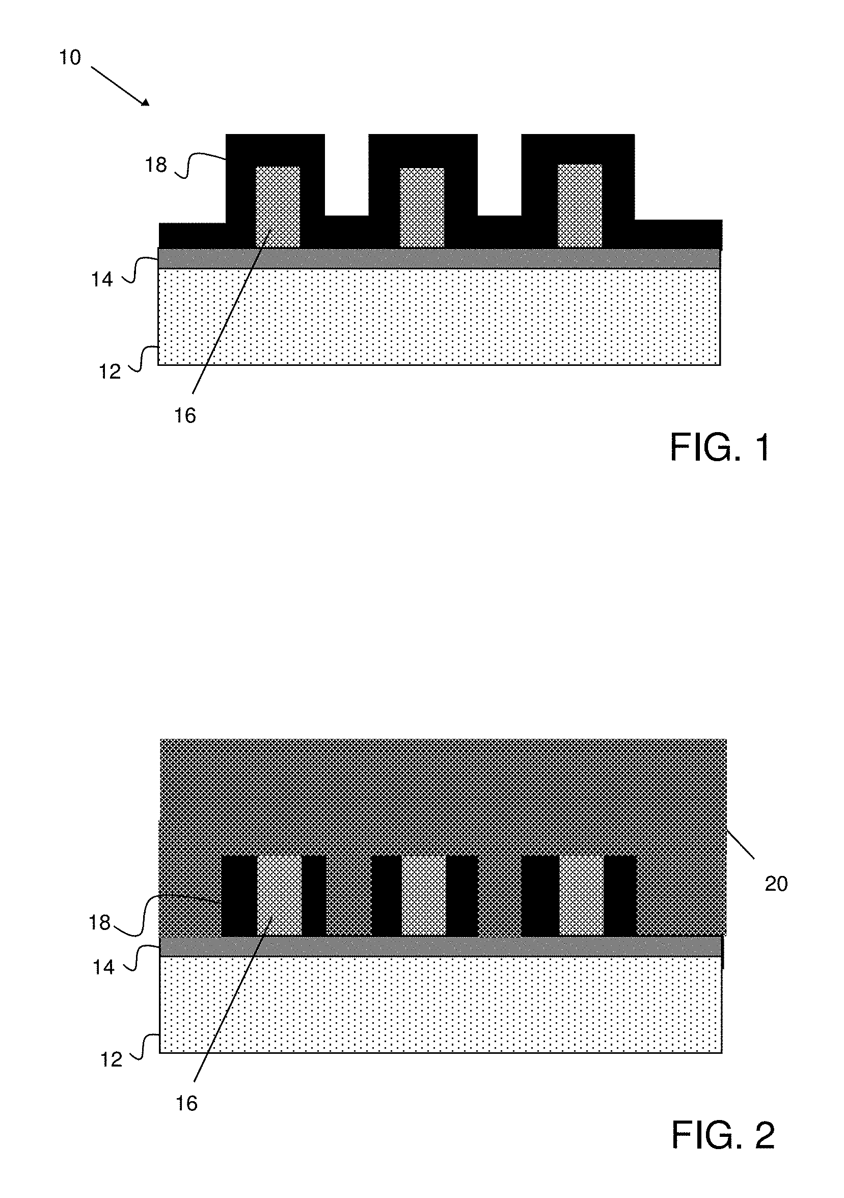
FIG. 1 shows a mandrel with spacers, amongst other features, and respective fabrication processes in accordance with aspects of the disclosure.
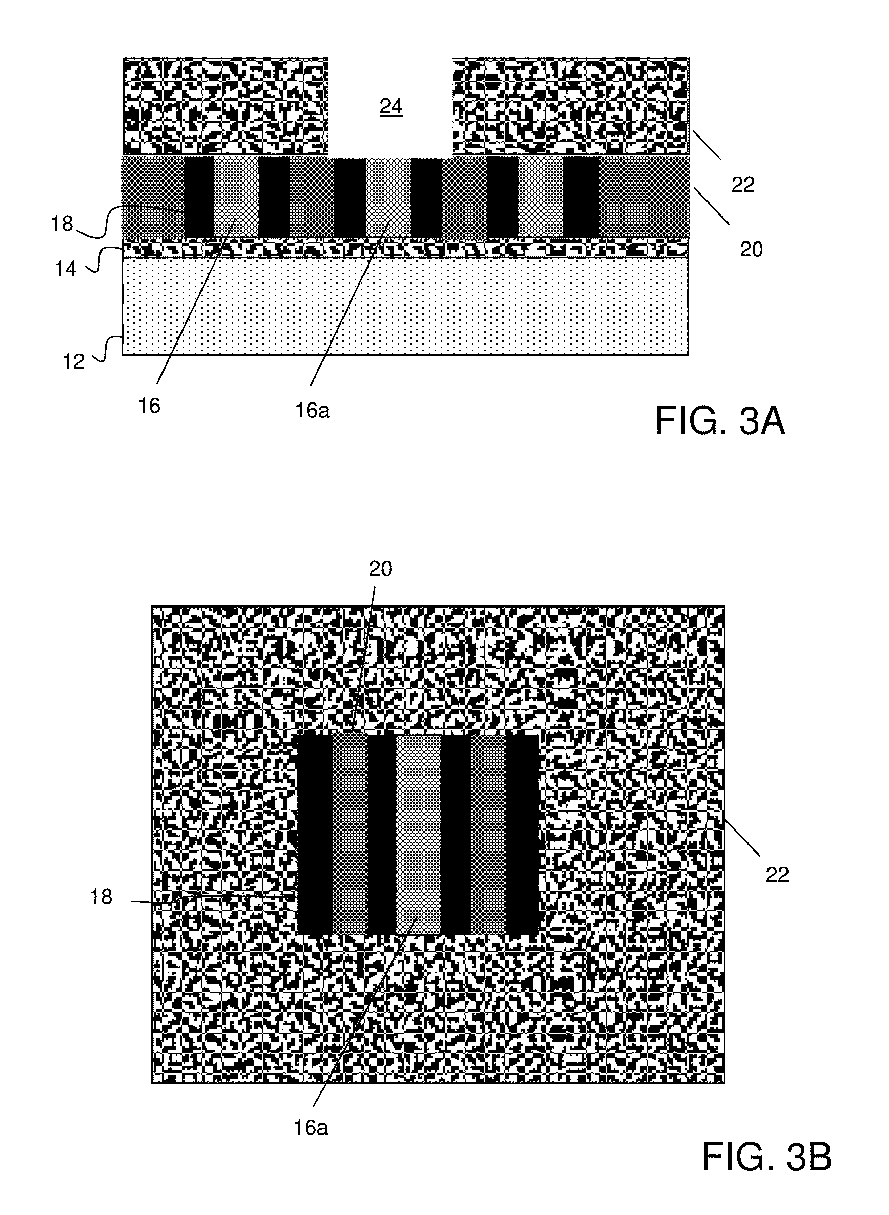
FIG. 2 shows a coating applied over spacer material, amongst other features, and respective fabrication processes in accordance with aspects of the disclosure.
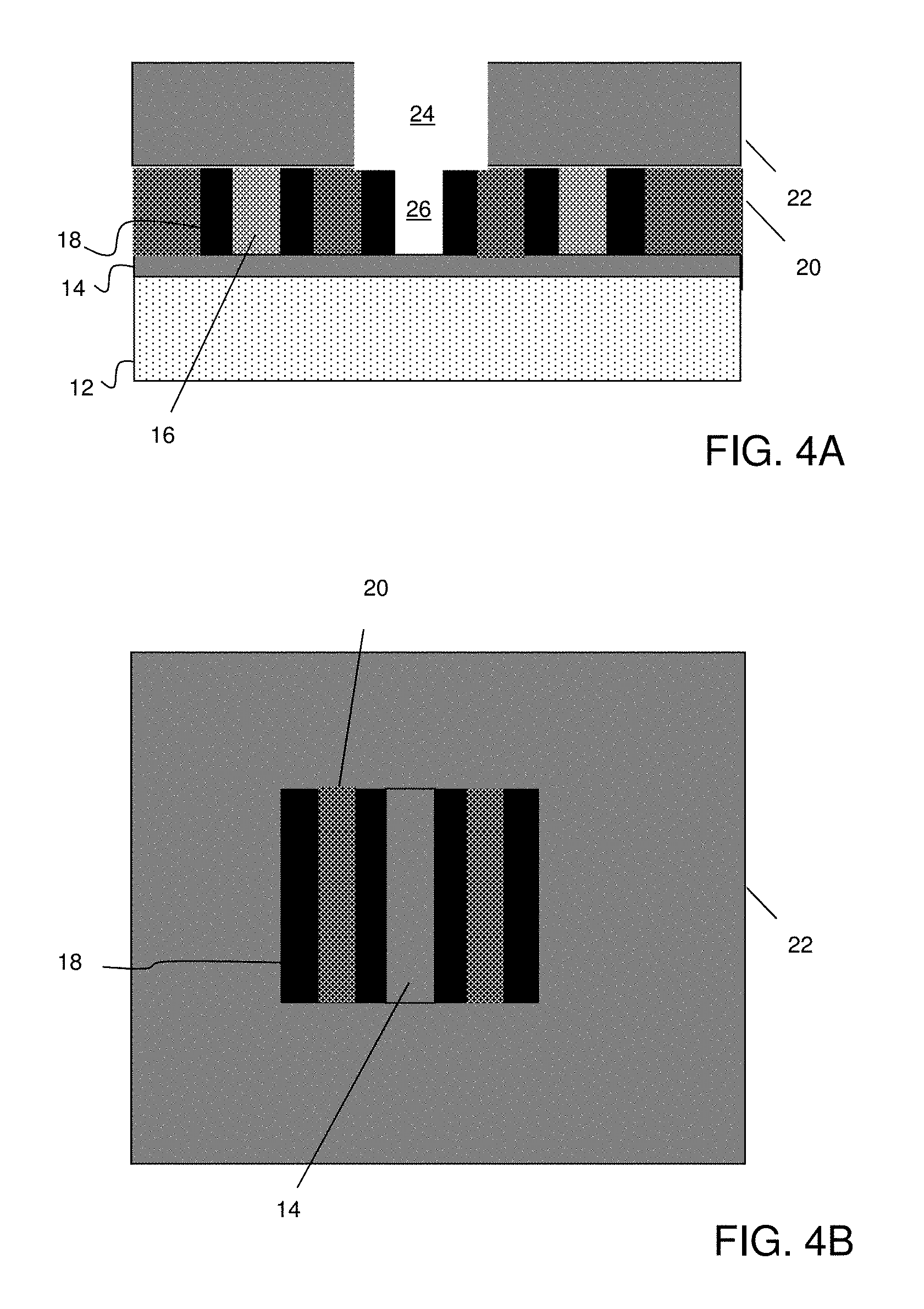
FIG. 3A shows an opening in mask material, amongst other features, and respective fabrication processes in accordance with aspects of the disclosure.
FIG. 3B shows a top view of FIG. 3A.
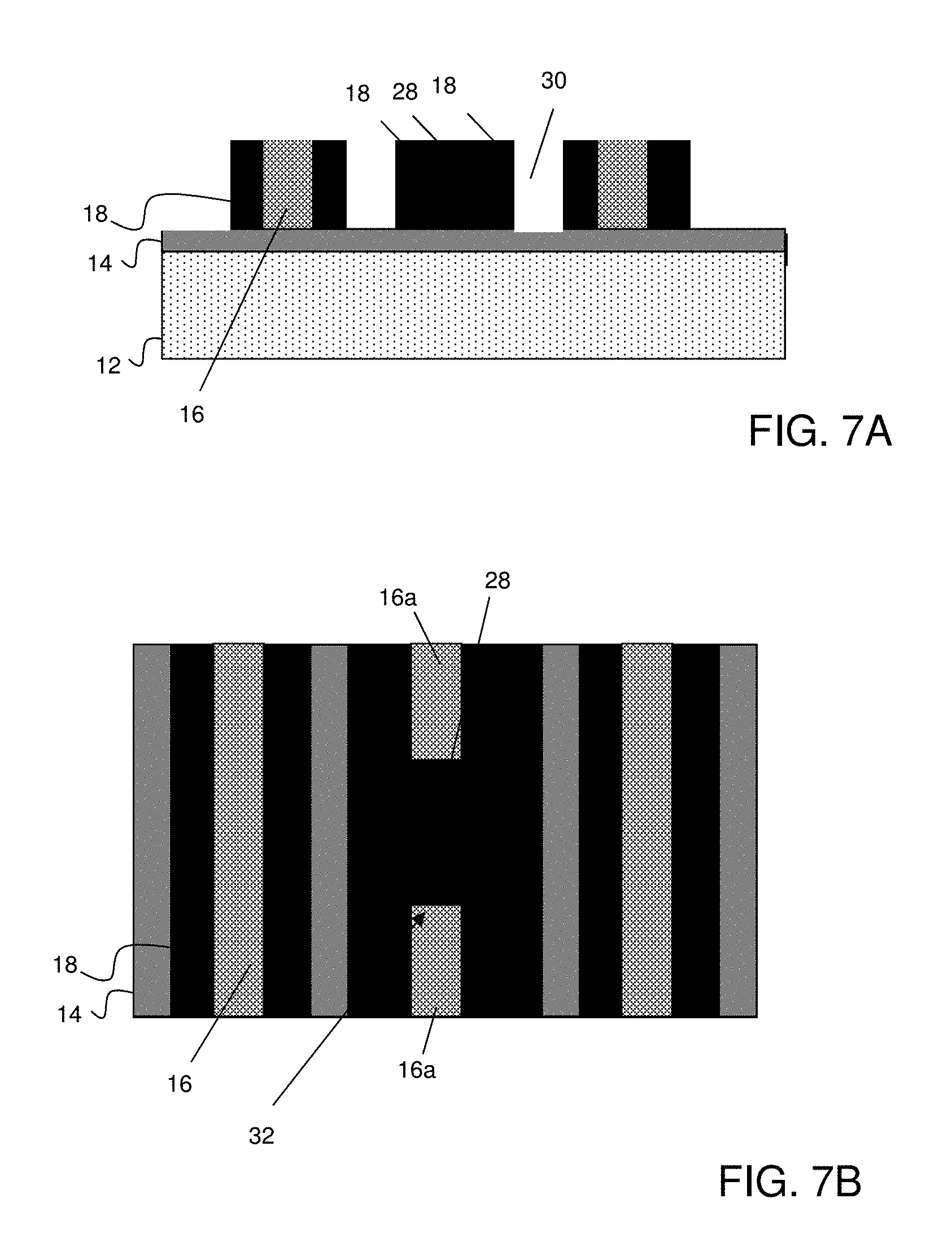
FIG. 4A shows a cut in a mandrel, amongst other features, and respective fabrication processes in accordance with aspects of the disclosure.
FIG. 4B shows a top view of FIG. 4A.
FIG. 5 shows material in a trench (cut) formed by the removal of a portion of the mandrel, amongst other features, and respective fabrication processes in accordance with aspects of the disclosure.
FIG. 6 shows an opening exposing the material and spacer material, amongst other features, and respective fabrication processes in accordance with aspects of the disclosure.
FIGS. 7A and 7B show spaces between mandrels, amongst other features, and respective fabrication processes in accordance with aspects of the disclosure.
FIGS. 8A-8J show an exemplary, non-limiting example of a two cut variable tip to tip non-mandrel structures and respective fabrication processes that are performed after the variable space mandrel cut for self-aligned double patterning described herein.
DETAILED DESCRIPTION
The present disclosure relates to semiconductor structures and, more particularly, to variable space mandrel cut for self-aligned double patterning and methods of manufacture. More specifically, the present disclosure provides a method of manufacturing variable space at the mandrel to improve design flexibility. Advantageously, by providing the variable space at the mandrel, it is now possible to further reduce parasitic capacitance of the structure.
In embodiments, the methods described herein provide a fabrication process to pattern a variable tip to tip space at the mandrel and fill the cut area (along a length of the mandrel) with a same material as spacer to define the mandrel cut. In embodiments, the mandrel can be, e.g., amorphous silicon (a-Si) with a TiOx spacer. By using the combination of materials and the processes described herein, it is possible to reduce parasitic capacitance of the structure by about an additional 3%.
The structures of the present disclosure can be manufactured in a number of ways using a number of different tools. In general, though, the methodologies and tools are used to form structures with dimensions in the micrometer and nanometer scale. The methodologies, i.e., technologies, employed to manufacture the structures of the present disclosure have been adopted from integrated circuit (IC) technology. For example, the structures are built on wafers and are realized in films of material patterned by photolithographic processes on the top of a wafer. In particular, the fabrication of the structures uses three basic building blocks: (i) deposition of thin films of material on a substrate, (ii) applying a patterned mask on top of the films by photolithographic imaging, and (iii) etching the films selectively to the mask.
FIG. 1 shows a structure and respective fabrication processes in accordance with aspects of the disclosure. In embodiments, the structure 10 includes a back end of the line (BEOL) substrate 14 formed on a substrate 12. In embodiments, the BEOL substrate 14 can be a hardmask such as, e.g., SiO.sub.2 or TiN, which can be later removed during conventional variable tip to tip non-mandrel processes of record. The substrate 12 can be dielectric material, e.g., low-k dielectric material, with wiring lines, e.g., copper or other metal lines.
Still referring to FIG. 1, a plurality of mandrels 16 are formed on the BEOL substrate 14. In embodiments, the mandrels 16 can be Si or C based materials; although other materials are also contemplated herein. The mandrels 16 can be formed by conventional deposition processes, e.g., chemical vapor deposition (CVD), followed by lithography and etching processes. For example, after deposition of the material on the BEOL substrate 14, a resist formed over the material is exposed to energy (light) to form a pattern (opening). An etching process with a selective chemistry, e.g., reactive ion etching (RIE), will be used to form one or more spaces in the material through the openings of the resist. The space between adjacent mandrels 16 can be about 3.times. the thickness of the mandrel 16. The resist can then be removed by a conventional oxygen ashing process or other known stripants.
Following the resist removal, spacer material 18 is formed on the mandrels 16 and exposed portions of the BEOL substrate 14. In embodiments, the spacer material 18 can be, e.g., TiO.sub.x, deposited by a conventional deposition process, e.g., CVD or atomic layer deposition (ALD) processes. The spacer material 18 can have a thickness approximately or substantially equal to the thickness of the mandrel 16, hence leaving a space between the spacer material which is approximately the same dimensions of the mandrel 16.
In FIG. 2, the spacer material 18 undergoes an anisotropic etching process to remove material over horizontal surfaces; that is, an anisotropic etching process removes material over the BEOL substrate 14 and a top surface of the mandrels 16. In this way, a surface of the BEOL substrate 14 and a top surface of the mandrels 16 will be exposed for further processing steps. A coating 20 is applied over the spacer material 18, exposed portions of the BEOL substrate 14 and a top surface of the mandrels 16. The coating 20 can be a spin on glass. For example, the coating 20 can be SiO.sub.2 or SiOC, deposited using an atomic layer deposition (ALD) process or other spin-on-glass deposition process.
FIG. 3A shows a cross-sectional view of the structure after further processing; whereas, FIG. 3B shows a top view of FIG. 3A. More specifically, in FIGS. 3A and 3B, the coating 20 undergoes a back etch process, e.g., dry etch process. In embodiments, the back etching will result in the coating 20 being removed above the spacer material 18, exposing the top surface of the mandrels 16. The etching process will result in the coating 20, the top surfaces of the mandrels 16 and spacer material 18 forming a planar surface.
Still referring to FIGS. 3A and 3B, a photolithographic stack of material 22 is formed on the planar surface of the coating 20, top surface of the mandrels 16 and spacer material 18. An opening 24 is formed in the photolithographic stack of material 22 in alignment with mandrel 16a. The photolithographic stack of material 22 can be, e.g., SOH, SiON, ARC material, etc. which is opened using conventional lithographic processes, e.g., exposure to energy. In embodiments, the opening 24 can slightly overlap the coating material 20 adjacent to the spacer material 18. For example, in embodiments, the opening 24 can be, e.g., greater than 2.times. the width of the spacer material 18. In embodiments, the opening can expose a portion of the spacer material 18 and a portion of the mandrel 16a, which can be later removed to form a cut.
FIG. 4A shows a cross-sectional view of the structure after mandrel pull processing; whereas, FIG. 4B shows a top view of FIG. 4A. More specifically, in FIGS. 4A and 4B, an exposed portion of the mandrel 16a is removed by a selective etch chemistry. The removal of the exposed portion of the mandrel 16a will result in a trench or cut 26 along a length of the mandrel 16a, exposing the underlying BEOL substrate 14. It should be recognized, though, that remaining portions of the mandrel 16a remain protected under the photolithographic stack of material 22.
In FIG. 5, a material 28 is deposited within the opening 24 and cut 26 formed by partial removal of the mandrel 16a. In embodiments, the material 28 is the same material as the spacer material 18, e.g., TiO.sub.x, which can be a flowable material or deposited by conventional ALD processes. In alternative embodiments, the spacer material 18 and the material 28 can be TiN or other metals that are selective to the mandrel material.
As further shown in FIG. 6, the material 28 can be etched backed to a top surface of the spacer material 18, coating 20 and mandrels 16, 16a. In embodiments, the etch back can be a timed etch to stop on the coating 20 or an end point etch which detects the chemistry difference when the coating 20 begins to etch back. In either scenario, a slight etch back of the coating 20 or spacers 18 will not significantly affect the performance of the end product device.
FIG. 7A shows a cross sectional view of the structure after removal of the spin on glass material; whereas, FIG. 7B shows a top view of FIG. 7A. More specifically, as shown in FIGS. 7A and 7B, the photolithographic stack of material 22 can be removed by conventional stripping techniques. Following this removal, the spin on glass material, e.g., material 20, can be removed by a selective chemistry. The resultant structure includes spaces 30 between adjacent spacer material 18 and a cut 32 between adjacent portions of a mandrel 16a, along a length thereof, filled with material 28. In embodiments, the cut 32 can be 2.times. or more of the thickness of the spacer material 18. In embodiments, the additional material 28 can reduce parasitic capacitance of the structure by about an additional 3%.
FIGS. 8A-8J show an exemplary, non-limiting example of a two cut variable tip to tip non-mandrel structures and respective fabrication processes that are performed after the variable space mandrel cut for self-aligned double patterning described herein. Specifically, FIG. 8A shows a patterned photoresist 100. FIG. 8B shows a plurality of mandrels 105 formed, and removal of the patterned photoresist 100. The mandrels 105 can be formed by conventional deposition processes, followed by resist removal. In FIG. 8C, a photolithographic mask 110 is formed over the mandrels 105. In FIG. 8D, the mandrels 105 are cut by conventional etching processes. The space (e.g., cut) 115 between the mandrels is less than 2.times. a spacer width. As further shown in FIG. 8E, a spacer material 120 is deposited between the mandrels 105 and within the spaces 115. A photolithographic mask 125 is formed over the structure (FIG. 8F), followed by a cut spacer 130 formation (FIGS. 8G and 8H). In FIG. 8I, a block photolithographic hardmask 135 is formed by conventional deposition processes, followed by a copper fill 140 and low-k dielectric material 145 (FIG. 8J).
The method(s) as described above is used in the fabrication of integrated circuit chips. The resulting integrated circuit chips can be distributed by the fabricator in raw wafer form (that is, as a single wafer that has multiple unpackaged chips), as a bare die, or in a packaged form. In the latter case the chip is mounted in a single chip package (such as a plastic carrier, with leads that are affixed to a motherboard or other higher level carrier) or in a multichip package (such as a ceramic carrier that has either or both surface interconnections or buried interconnections). In any case the chip is then integrated with other chips, discrete circuit elements, and/or other signal processing devices as part of either (a) an intermediate product, such as a motherboard, or (b) an end product. The end product can be any product that includes integrated circuit chips, ranging from toys and other low-end applications to advanced computer products having a display, a keyboard or other input device, and a central processor.
The descriptions of the various embodiments of the present disclosure have been presented for purposes of illustration, but are not intended to be exhaustive or limited to the embodiments disclosed. Many modifications and variations will be apparent to those of ordinary skill in the art without departing from the scope and spirit of the described embodiments. The terminology used herein was chosen to best explain the principles of the embodiments, the practical application or technical improvement over technologies found in the marketplace, or to enable others of ordinary skill in the art to understand the embodiments disclosed herein.
* * * * *
D00000
D00001
D00002
D00003
D00004
D00005
D00006
XML
uspto.report is an independent third-party trademark research tool that is not affiliated, endorsed, or sponsored by the United States Patent and Trademark Office (USPTO) or any other governmental organization. The information provided by uspto.report is based on publicly available data at the time of writing and is intended for informational purposes only.
While we strive to provide accurate and up-to-date information, we do not guarantee the accuracy, completeness, reliability, or suitability of the information displayed on this site. The use of this site is at your own risk. Any reliance you place on such information is therefore strictly at your own risk.
All official trademark data, including owner information, should be verified by visiting the official USPTO website at www.uspto.gov. This site is not intended to replace professional legal advice and should not be used as a substitute for consulting with a legal professional who is knowledgeable about trademark law.