Systems and methods for ultrahigh selective nitride etch
Yang , et al. Ja
U.S. patent number 10,192,751 [Application Number 15/271,381] was granted by the patent office on 2019-01-29 for systems and methods for ultrahigh selective nitride etch. This patent grant is currently assigned to LAM RESEARCH CORPORATION. The grantee listed for this patent is Lam Research Corporation. Invention is credited to Joon Hong Park, Pilyeon Park, Dengliang Yang, Faisal Yaqoob, Helen H. Zhu.


| United States Patent | 10,192,751 |
| Yang , et al. | January 29, 2019 |
Systems and methods for ultrahigh selective nitride etch
Abstract
A method for selectively etching a silicon nitride layer on a substrate includes arranging a substrate on a substrate support of a substrate processing chamber. The substrate processing chamber includes an upper chamber region, an inductive coil arranged outside of the upper chamber region, a lower chamber region including the substrate support and a gas dispersion device. The gas dispersion device includes a plurality of holes in fluid communication with the upper chamber region and the lower chamber region. The method includes supplying an etch gas mixture to the upper chamber region and striking inductively coupled plasma in the upper chamber region by supplying power to the inductive coil. The etch gas mixture etches silicon nitride, promotes silicon dioxide passivation and promotes polysilicon passivation. The method includes selectively etching the silicon nitride layer on the substrate and extinguishing the inductively coupled plasma after a predetermined period.
| Inventors: | Yang; Dengliang (Union City, CA), Yaqoob; Faisal (Fremont, CA), Park; Pilyeon (Santa Clara, CA), Zhu; Helen H. (Fremont, CA), Park; Joon Hong (Dublin, CA) | ||||||||||
|---|---|---|---|---|---|---|---|---|---|---|---|
| Applicant: |
|
||||||||||
| Assignee: | LAM RESEARCH CORPORATION
(Fremont, CA) |
||||||||||
| Family ID: | 58524280 | ||||||||||
| Appl. No.: | 15/271,381 | ||||||||||
| Filed: | September 21, 2016 |
Prior Publication Data
| Document Identifier | Publication Date | |
|---|---|---|
| US 20170110335 A1 | Apr 20, 2017 | |
Related U.S. Patent Documents
| Application Number | Filing Date | Patent Number | Issue Date | ||
|---|---|---|---|---|---|
| 62241827 | Oct 15, 2015 | ||||
| Current U.S. Class: | 1/1 |
| Current CPC Class: | H01J 37/321 (20130101); H01L 21/31116 (20130101); H01J 2237/334 (20130101) |
| Current International Class: | H01L 21/311 (20060101); H01J 37/32 (20060101) |
| Field of Search: | ;216/68 ;438/724 |
References Cited [Referenced By]
U.S. Patent Documents
| 4374698 | February 1983 | Sanders et al. |
| 4431477 | February 1984 | Zajac |
| 4793897 | December 1988 | Dunfield et al. |
| 5329965 | July 1994 | Gordon |
| 5605179 | February 1997 | Strong, Jr. et al. |
| 5662143 | September 1997 | Caughran |
| 5744695 | April 1998 | Forbes |
| 6042687 | March 2000 | Singh et al. |
| 6060400 | May 2000 | Oehrlein et al. |
| 6074959 | June 2000 | Wang et al. |
| 6152168 | November 2000 | Ohmi et al. |
| 6376386 | April 2002 | Oshima |
| 6841943 | January 2005 | Vahedi et al. |
| 6962879 | November 2005 | Zhu et al. |
| 7129171 | October 2006 | Zhu et al. |
| 7288482 | October 2007 | Panda et al. |
| 7309646 | December 2007 | Heo et al. |
| 7338907 | March 2008 | Li et al. |
| 7757541 | July 2010 | Monkowski et al. |
| 7758698 | July 2010 | Bang et al. |
| 8137463 | March 2012 | Liu et al. |
| 8552334 | October 2013 | Tappan et al. |
| 8555920 | October 2013 | Hirata et al. |
| 8592328 | November 2013 | Hausmann et al. |
| 8889024 | November 2014 | Watanabe et al. |
| 8956980 | February 2015 | Chen et al. |
| 9051647 | June 2015 | Cooperberg et al. |
| 9059678 | June 2015 | Long et al. |
| 9318343 | April 2016 | Ranjan et al. |
| 9471065 | October 2016 | Koyomogi et al. |
| 9640409 | May 2017 | Yang et al. |
| 2001/0002581 | June 2001 | Nishikawa et al. |
| 2001/0004903 | June 2001 | Ohmi et al. |
| 2001/0013363 | August 2001 | Kitayama et al. |
| 2002/0038669 | April 2002 | Yamagishi et al. |
| 2002/0042205 | April 2002 | McMillin et al. |
| 2002/0046991 | April 2002 | Smith et al. |
| 2002/0088542 | July 2002 | Nishikawa |
| 2002/0160125 | October 2002 | Johnson et al. |
| 2002/0174905 | November 2002 | Latino et al. |
| 2002/0175144 | November 2002 | Hung et al. |
| 2003/0236592 | December 2003 | Shajii et al. |
| 2003/0236638 | December 2003 | Shajil et al. |
| 2003/0236643 | December 2003 | Shajii et al. |
| 2004/0094206 | May 2004 | Ishida |
| 2004/0112538 | June 2004 | Larson et al. |
| 2004/0112539 | June 2004 | Larson et al. |
| 2004/0112540 | June 2004 | Larson et al. |
| 2004/0168719 | September 2004 | Nambu |
| 2004/0173270 | September 2004 | Harris et al. |
| 2005/0005994 | January 2005 | Sugiyama et al. |
| 2005/0067021 | March 2005 | Bevers et al. |
| 2005/0155625 | July 2005 | Jangjian et al. |
| 2005/0199342 | September 2005 | Shajii et al. |
| 2005/0241763 | November 2005 | Huang et al. |
| 2006/0011237 | January 2006 | Tison et al. |
| 2006/0097644 | May 2006 | Kono et al. |
| 2006/0124169 | June 2006 | Mizusawa et al. |
| 2006/0207595 | September 2006 | Ohmi et al. |
| 2006/0237063 | October 2006 | Ding et al. |
| 2007/0026684 | February 2007 | Parascandola et al. |
| 2007/0066038 | March 2007 | Sadjadi et al. |
| 2007/0158025 | July 2007 | Larson |
| 2007/0233412 | October 2007 | Gotoh et al. |
| 2007/0240778 | October 2007 | L'Bassi et al. |
| 2007/0259112 | November 2007 | Ishikawa et al. |
| 2008/0115834 | May 2008 | Geoffrion et al. |
| 2008/0121178 | May 2008 | Bang et al. |
| 2008/0202588 | August 2008 | Gold et al. |
| 2008/0202609 | August 2008 | Gold et al. |
| 2008/0202610 | August 2008 | Gold et al. |
| 2009/0061083 | March 2009 | Chiang et al. |
| 2009/0061640 | March 2009 | Wong et al. |
| 2009/0061644 | March 2009 | Chiang et al. |
| 2009/0183548 | July 2009 | Monkowski et al. |
| 2009/0183549 | July 2009 | Monkowski et al. |
| 2009/0221117 | September 2009 | Tan et al. |
| 2009/0272717 | November 2009 | Pamarthy et al. |
| 2009/0320754 | December 2009 | Oya et al. |
| 2010/0030390 | February 2010 | Yamaguchi et al. |
| 2010/0071438 | March 2010 | Davis et al. |
| 2010/0145633 | June 2010 | Yasuda |
| 2010/0178770 | July 2010 | Zin |
| 2010/0229976 | September 2010 | Hirata et al. |
| 2010/0269924 | October 2010 | Yasuda |
| 2011/0019332 | January 2011 | Chistyakov |
| 2011/0094596 | April 2011 | Sugiyarna et al. |
| 2011/0253225 | October 2011 | Beeby et al. |
| 2012/0031500 | February 2012 | Hirose et al. |
| 2012/0034786 | February 2012 | Dhindsa et al. |
| 2012/0149213 | June 2012 | Nittala et al. |
| 2012/0152364 | June 2012 | Hashimoto et al. |
| 2012/0174990 | July 2012 | Yasuda |
| 2012/0190208 | July 2012 | Ozu et al. |
| 2012/0238102 | September 2012 | Zhang et al. |
| 2012/0238103 | September 2012 | Zhang et al. |
| 2012/0244715 | September 2012 | Lebouitz et al. |
| 2012/0289057 | November 2012 | DeDontney |
| 2012/0298221 | November 2012 | Takeuchi et al. |
| 2013/0008607 | January 2013 | Matsumoto et al. |
| 2013/0025715 | January 2013 | Yamaguchi et al. |
| 2013/0029494 | January 2013 | Sasaki et al. |
| 2013/0045605 | February 2013 | Wang et al. |
| 2013/0131300 | May 2013 | Olmscheid et al. |
| 2013/0145816 | June 2013 | Lowe |
| 2013/0220433 | August 2013 | Sawada et al. |
| 2013/0270997 | October 2013 | Zhao et al. |
| 2014/0080308 | March 2014 | Chen et al. |
| 2014/0120737 | May 2014 | Swaminathan et al. |
| 2014/0141621 | May 2014 | Ren et al. |
| 2014/0182689 | July 2014 | Shareef et al. |
| 2014/0248780 | September 2014 | Ingle et al. |
| 2014/0262038 | September 2014 | Wang et al. |
| 2015/0017810 | January 2015 | Guha |
| 2015/0059859 | March 2015 | Takahashi et al. |
| 2015/0287572 | October 2015 | Daugherty et al. |
| 2016/0181116 | June 2016 | Berry, III et al. |
| 2016/0215392 | July 2016 | Yudovsky et al. |
| 2016/0247688 | August 2016 | Zhu et al. |
| 2017/0032982 | February 2017 | Drewery et al. |
| 2017/0069511 | March 2017 | Yang et al. |
| 2017/0200586 | July 2017 | Treadwell et al. |
| 2017/0236694 | August 2017 | Eason et al. |
| 0424299 | Apr 1991 | EP | |||
| 0424299 | Aug 1991 | EP | |||
| 0838842 | Apr 1998 | EP | |||
| WO-0040776 | Jul 2000 | WO | |||
| WO-2011051251 | May 2011 | WO | |||
| WO-2013123617 | Aug 2013 | WO | |||
| WO-2014068886 | May 2014 | WO | |||
Other References
|
US. Appl. No. 15/399,692, Treadwell et al. cited by applicant . Blain (Mar./Apr. 1999) "Mechanism of nitrogen removal from silicon nitride by nitric oxide," Journal of Vacuum Science & Technology A, 17(2):665-667. cited by applicant . Blain et al. (Jul./Aug. 1996) "Role of nitrogen in the downstream etching of silicon nitride," Journal of Vacuum Science & Technology A, 14(4):2151-2157. cited by applicant . Bohr, Mark, "The New Era of Scaling in an SoC World" Intel Logic Technology Development; ISSCC; 2009; 66 Pages. cited by applicant . Dusa, Mircean et al., "Pitch Doubling Through Dual Patterning Lithography Challenges in Integration and Litho Budgets," Optical Microlithography XX, vol. 6520, 65200G, (2007); 10 pages. cited by applicant . European Extended Search Report dated May 30, 2016 issued in EP 15 199 363.1 [LAMRP146EP]. cited by applicant . Kastenmeier et al. (Nov./Dec. 1999) "Highly selective etching of silicon nitride over silicon and silicon dioxide," J. Vac. Sci. Technol. A, American Vacuum Society , 17 (6):3179-3184. cited by applicant . Kastenmeier et al. (Sep./Oct. 1996) "Chemical dry etching of silicon nitride and silicon dioxide using CF4/02/N2 gas mixtures," J. Vac. Sci, Technol. A14(5):2802-2813. cited by applicant . Oehrlein et al. (1996) "Study of plasma-surface interactions: chemical dry etching and high-density plasma etching," Plasma Sources Sci. Technol. 5:193-199. cited by applicant . Tajima et al. (2013) "Room-Temperature Si Etching in NO/F2 Gases and the Investigation of Surface Reaction Mechanisms," The Journal of Physical Chemistry C, 117:5118-5125. cited by applicant . U.S. Office Action dated Oct. 5, 2015 issued in U.S. Appl. No. 14/576,020 [LAMRP146]. cited by applicant . U.S. Final Office Action dated Feb. 26, 2016 issued in U.S. Appl. No. 14/576,020 [LAMRP146]. cited by applicant . U.S. Office Action dated Sep. 23, 2016 issued in U.S. Appl. No. 14/576,020 [LAMRP146]. cited by applicant . Yun et al. (2007) "Large Etch Rate Enhancement by NO-Induced Surface Chemical Reaction during Chemical Dry Etching of Silicon Oxide in F2 Remote Plasmas," Journal of the Electrochemical Society, 154(4):D267-D272. cited by applicant . U.S. Appl. No. 15/014,539, filed Feb. 3, 2016, Yang et al. cited by applicant . U.S. Appl. No. 14/945,680, filed Nov. 19, 2015, Drewery et al. cited by applicant . U.S. Appl. No. 15/399,692, filed Jan. 7, 2016, Treadwell et al. cited by applicant . U.S. Appl. No. 62/106,407: filed Jan. 22, 2015, in the names of Joseph Yudovsky et al., & entitled "Injector for Spatially Separated Atomic Layer Deposition Chamber" pp. 1-68. (Year: 2015). cited by applicant. |
Primary Examiner: Culbert; Roberts P
Parent Case Text
CROSS-REFERENCE TO RELATED APPLICATIONS
This application claims the benefit of U.S. Provisional Application No. 62/241,827, filed on Oct. 15, 2015. The entire disclosure of the application referenced above is incorporated herein by reference.
Claims
What is claimed is:
1. A method for selectively etching a silicon nitride layer on a substrate, comprising: arranging the substrate on a substrate support of a substrate processing chamber, wherein the substrate processing chamber includes an upper chamber region, an inductive coil arranged outside of the upper chamber region, a lower chamber region including the substrate support and a gas dispersion device arranged between the upper chamber region and the lower chamber region, and wherein the gas dispersion device includes a plurality of holes in fluid communication with the upper chamber region and the lower chamber region; supplying an etch gas mixture to the upper chamber region; striking inductively coupled plasma in the upper chamber region by supplying power to the inductive coil, wherein the etch gas mixture etches silicon nitride, promotes silicon dioxide passivation and promotes polysilicon passivation; selectively etching the silicon nitride layer on the substrate; extinguishing the inductively coupled plasma after a predetermined period; and after the selectively etching, dry cleaning the substrate by supplying a dry clean gas mixture to the substrate processing chamber and striking plasma in the substrate processing chamber for another predetermined period.
2. The method of claim 1, wherein the etch gas mixture includes a silicon nitride etch promoter including at least one gas selected from a group consisting of nitrogen trifluoride (NF.sub.3), difluoromethane (CH.sub.2F.sub.2), tetrafluoromethane (CF.sub.4), and fluoromethane (CH.sub.3F).
3. The method of claim 2, wherein the silicon nitride etch promoter includes at least one gas selected from a group consisting of molecular oxygen (O.sub.2), molecular nitrogen (N.sub.2), and nitrous oxide (N.sub.2O).
4. The method of claim 1, wherein the etch gas mixture includes a silicon dioxide passivation promoter including at least one gas selected from a group consisting of fluoromethane (CH.sub.3F) and difluoromethane (CH.sub.2F.sub.2).
5. The method of claim 4, wherein the silicon dioxide passivation promoter further includes at least one gas selected from a group consisting of molecular oxygen (O.sub.2), molecular nitrogen (N.sub.2), and nitrous oxide (N.sub.2O).
6. The method of claim 1, wherein the etch gas mixture includes a polysilicon passivation promoter including at least one gas selected from a group consisting of molecular oxygen (O.sub.2), molecular nitrogen (N.sub.2), and nitrous oxide (N.sub.2O).
7. The method of claim 1, further comprising repeating the etching using the etch gas mixture and the dry cleaning using the dry clean gas mixture one or more times.
8. The method of claim 7, wherein the dry clean gas mixture includes at least one gas selected from a group consisting of carbon dioxide (CO.sub.2) and carbon monoxide (CO).
9. The method of claim 8, wherein the dry clean gas mixture further includes at least one gas selected from a group including argon (Ar), Neon (Ne) and Helium (He).
10. The method of claim 1, wherein the dry clean gas mixture includes at least one gas selected from a group consisting of molecular nitrogen (N.sub.2) or nitrous oxide (N.sub.2O).
11. The method of claim 1, wherein pressure in the substrate processing chamber is in a pressure range from 0.5 to 5 Torr.
12. The method of claim 1, wherein a radio frequency (RF) bias is supplied to the substrate support during the etching.
13. The method of claim 1, wherein a radio frequency (RF) bias is not supplied to the substrate support during the etching.
14. The method of claim 1, wherein the gas dispersion device includes a showerhead including a plurality of holes.
15. The method of claim 14, wherein the plurality of holes have diameters in a range from 0.1'' to 0.75''.
16. The method of claim 1, further comprising grounding the gas dispersion device during the etching.
17. The method of claim 1, wherein the etch gas mixture includes nitrogen trifluoride (NF.sub.3), difluoromethane (CH.sub.2F.sub.2), molecular oxygen (O.sub.2), molecular nitrogen (N.sub.2), nitrous oxide (N.sub.2O) and carbon dioxide (CO.sub.2).
18. The method of claim 1, wherein the etch gas mixture includes tetrafluoromethane (CF.sub.4), and fluoromethane (CH.sub.3F), molecular oxygen (O.sub.2), molecular nitrogen (N.sub.2), nitrous oxide (N.sub.2O) and carbon dioxide (CO.sub.2).
19. The method of claim 1, wherein the silicon nitride layer on the substrate is etched selectively relative to silicon dioxide.
20. The method of claim 1, wherein the silicon nitride layer on the substrate is etched selectively relative to polysilicon.
21. The method of claim 1, wherein the silicon nitride layer on the substrate is etched selectively relative to silicon oxycarbide (SiOC).
22. The method of claim 1, wherein the silicon nitride layer on the substrate is etched selectively relative to hafnium oxide (HfO.sub.x).
23. The method of claim 1, wherein the silicon nitride layer on the substrate is etched selectively relative to titanium nitride (TiN).
24. The method of claim 1, wherein the silicon nitride layer on the substrate is etched selectively relative to tantalum nitride (TaN).
25. The method of claim 1, wherein the silicon nitride layer on the substrate is etched selectively relative to tungsten (W).
26. The method of claim 1, wherein the silicon nitride layer on the substrate is etched selectively relative to titanium aluminum nitride (TiAlN).
27. A method for selectively etching a silicon nitride layer on a substrate, comprising: arranging the substrate on a substrate support of a substrate processing chamber, wherein the substrate processing chamber includes an upper chamber region, an inductive coil arranged outside of the upper chamber region, a lower chamber region including the substrate support and a gas dispersion device arranged between the upper chamber region and the lower chamber region, and wherein the gas dispersion device includes a plurality of holes in fluid communication with the upper chamber region and the lower chamber region; supplying an etch gas mixture to the upper chamber region; striking inductively coupled plasma in the upper chamber region by supplying power to the inductive coil, wherein the etch gas mixture etches silicon nitride, promotes silicon dioxide passivation and promotes polysilicon passivation; selectively etching the silicon nitride layer on the substrate; and extinguishing the inductively coupled plasma after a predetermined period, wherein the etch gas mixture includes nitrogen trifluoride (NF.sub.3), difluoromethane (CH.sub.2F.sub.2), molecular oxygen (O.sub.2), molecular nitrogen (N.sub.2), nitrous oxide (N.sub.2O) and carbon dioxide (CO.sub.2); or wherein the etch gas mixture includes tetrafluoromethane (CF.sub.4), fluoromethane (CH.sub.3F), molecular oxygen (O.sub.2), molecular nitrogen (N.sub.2), nitrous oxide (N.sub.2O) and carbon dioxide (CO.sub.2).
28. A method for selectively etching a silicon nitride layer on a substrate, comprising: arranging the substrate on a substrate support of a substrate processing chamber, wherein the substrate processing chamber includes an upper chamber region, an inductive coil arranged outside of the upper chamber region, a lower chamber region including the substrate support and a gas dispersion device arranged between the upper chamber region and the lower chamber region, and wherein the gas dispersion device includes a plurality of holes in fluid communication with the upper chamber region and the lower chamber region; supplying an etch gas mixture to the upper chamber region; striking inductively coupled plasma in the upper chamber region by supplying power to the inductive coil, wherein the etch gas mixture etches silicon nitride, promotes silicon dioxide passivation and promotes polysilicon passivation; selectively etching the silicon nitride layer on the substrate; and extinguishing the inductively coupled plasma after a predetermined period, wherein the silicon nitride layer on the substrate is etched selectively relative to silicon oxycarbide (SiOC), hafnium oxide (HfO.sub.x), titanium nitride (TiN), tantalum nitride (TaN), or titanium aluminum nitride (TiAIN).
Description
FIELD
The present disclosure relates to substrate processing systems, and more particularly to systems and methods for selectively etching silicon nitride.
BACKGROUND
The background description provided here is for the purpose of generally presenting the context of the disclosure. Work of the presently named inventors, to the extent it is described in this background section, as well as aspects of the description that may not otherwise qualify as prior art at the time of filing, are neither expressly nor impliedly admitted as prior art against the present disclosure.
Substrate processing systems may be used to etch film on a substrate such as a semiconductor wafer. The substrate processing systems typically include a processing chamber, a gas distribution device and a substrate support. During processing, the substrate is arranged on the substrate support. Different gas mixtures may be introduced into the processing chamber and radio frequency (RF) plasma may be used to activate chemical reactions.
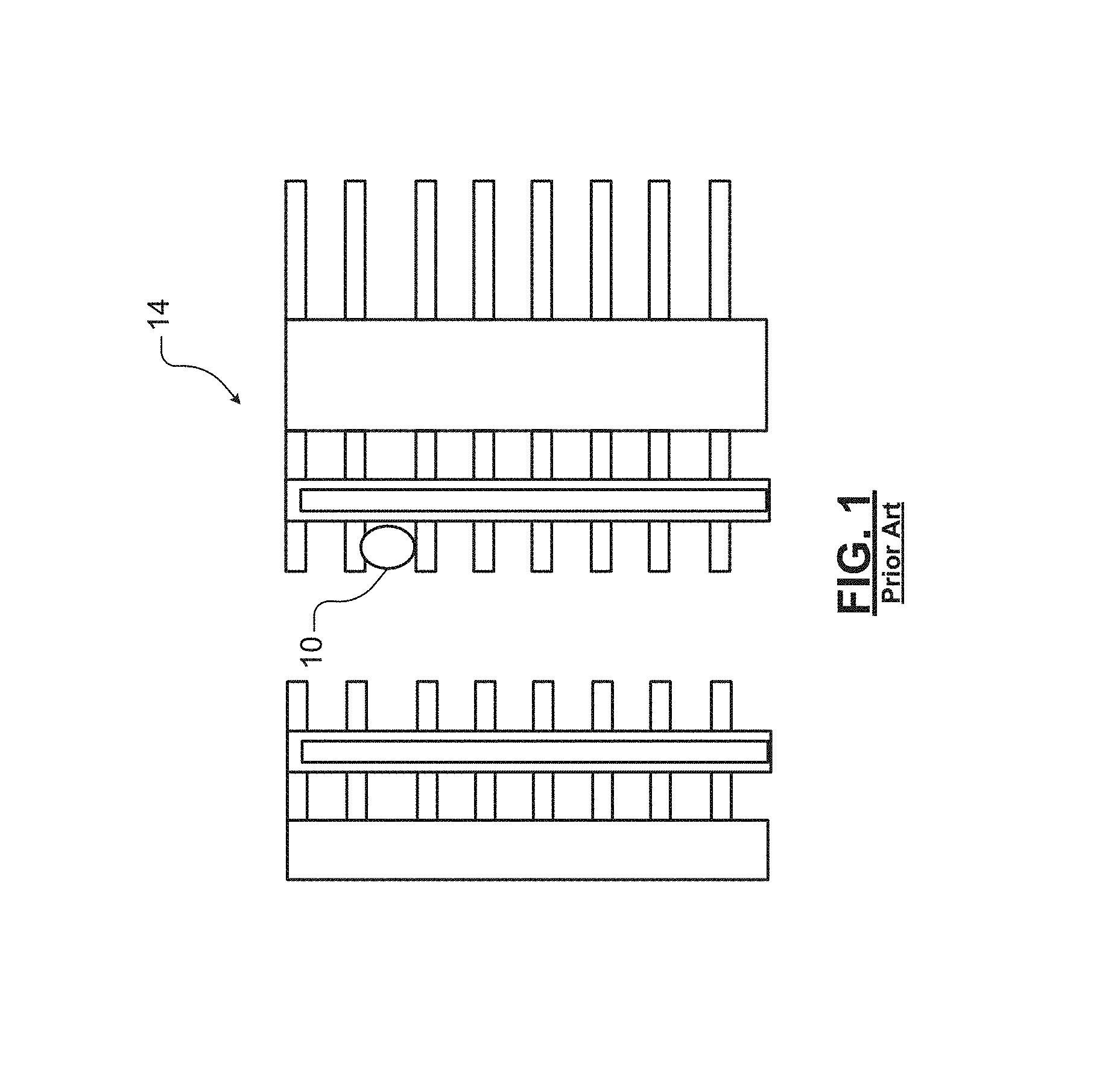
Referring now to FIG. 1, when integrating some semiconductor substrates such as vertical NAND devices, silicon nitride needs to be etched with very high selectivity to other exposed materials. Hot phosphoric acid is the main chemistry that is used for etching silicon nitride film in these devices. This etch process has several limitations that need to be addressed including the ability to scale above 36 layers, reducing defects and pitting, and improving control of the etch rate. For example in FIG. 1, a single defect particle 10 may cause loss of a write line string in a memory device 14.
SUMMARY
A method for selectively etching a silicon nitride layer on a substrate includes arranging a substrate on a substrate support of a substrate processing chamber. The substrate processing chamber includes an upper chamber region, an inductive coil arranged outside of the upper chamber region, a lower chamber region including the substrate support and a gas dispersion device arranged between the upper chamber region and the lower chamber region. The gas dispersion device includes a plurality of holes in fluid communication with the upper chamber region and the lower chamber region. The method includes supplying an etch gas mixture to the upper chamber region and striking inductively coupled plasma in the upper chamber region by supplying power to the inductive coil. The method includes selecting the etch gas mixture to etch silicon nitride, promote silicon dioxide passivation and promote polysilicon passivation. The method includes selectively etching the silicon nitride layer on the substrate and extinguishing the inductively coupled plasma after a predetermined period.
In other features, the etch gas mixture includes a silicon nitride etch promoter including at least one gas selected from a group consisting of nitrogen trifluoride (NF.sub.3), difluoromethane (CH.sub.2F.sub.2), tetrafluoro ethane (CF.sub.4), and fluoromethane (CH.sub.3F).
In other features, the silicon nitride etch promoter includes at least one gas selected from a group consisting of molecular oxygen (O.sub.2), molecular nitrogen (N.sub.2), and nitrous oxide (N.sub.2O).
In other features, the etch gas mixture includes a silicon dioxide passivation promoter including at least one gas selected from a group consisting of fluoromethane (CH.sub.3F) and difluoromethane (CH.sub.2F.sub.2).
In other features, the silicon dioxide passivation promoter further includes at least one gas selected from a group consisting of molecular oxygen (O.sub.2), molecular nitrogen (N.sub.2), and nitrous oxide (N.sub.2O).
In other features, the etch gas mixture includes a polysilicon passivation promoter including at least one gas selected from a group consisting of molecular oxygen (O.sub.2), molecular nitrogen (N.sub.2), and nitrous oxide (N.sub.2O).
In other features, the method includes, after the selectively etching, dry cleaning the substrate by supplying a dry clean gas mixture to the substrate processing chamber and striking plasma in the substrate processing chamber for a predetermined period.
In other features, the method includes repeating the etching using the etch gas mixture and the dry cleaning using the dry clean gas mixture one or more times.
In other features, the dry clean gas mixture includes at least one gas selected from a group consisting of carbon dioxide (CO.sub.2) and carbon monoxide (CO). The dry clean gas mixture further includes a gas such as argon (Ar), Helium (He), Neon (Ne), and/or other rare or Noble gases. The dry clean gas mixture includes at least one gas selected from a group consisting of molecular nitrogen (N.sub.2) or nitrous oxide (N.sub.2O).
In other features, pressure in the substrate processing chamber is in a pressure range from 0.5 to 5 Torr.
In other features, a radio frequency (RF) bias is supplied to the substrate support during the etching. A radio frequency (RF) bias is not supplied to the substrate support during the etching.
In other features, the gas dispersion device includes a showerhead including a plurality of holes. The plurality of holes has a diameter in a range from 0.1'' to 0.75''.
In other features, the method includes grounding the gas dispersion device during the etching.
In other features, the etch gas mixture includes nitrogen trifluoride (NF3), difluoromethane (CH2F2), molecular oxygen (O2), molecular nitrogen (N2), nitrous oxide (N2O) and carbon dioxide (CO.sub.2).
In other features, the etch gas mixture includes tetrafluoromethane (CF4), and fluoromethane (CH3F), molecular oxygen (O2), molecular nitrogen (N2), nitrous oxide (N2O) and carbon dioxide (CO.sub.2).
In other features, the silicon nitride layer on the substrate is etched selectively relative to silicon dioxide. The silicon nitride layer on the substrate is etched selectively relative to polysilicon. The silicon nitride layer on the substrate is etched selectively relative to silicon oxycarbide (SiOC). The silicon nitride layer on the substrate is etched selectively relative to hafnium oxide (HfOx).
In other features, the silicon nitride layer on the substrate is etched selectively relative to titanium nitride (TiN). The silicon nitride layer on the substrate is etched selectively relative to tantalum nitride (TaN). The silicon nitride layer on the substrate is etched selectively relative to tungsten (W). The silicon nitride layer on the substrate is etched selectively relative to titanium aluminum nitride (TiAlN).
Further areas of applicability of the present disclosure will become apparent from the detailed description, the claims and the drawings. The detailed description and specific examples are intended for purposes of illustration only and are not intended to limit the scope of the disclosure.
BRIEF DESCRIPTION OF THE DRAWINGS
The present disclosure will become more fully understood from the detailed description and the accompanying drawings, wherein:
FIG. 1 is a plan view illustrating a memory device having a defect particle shorting two write lines of a memory device according to the prior art;
FIG. 2 is a functional block diagram of an example of a substrate processing chamber for selectively etching silicon nitride and performing plasma dry cleaning according to the present disclosure;
FIGS. 3A-3B are flowcharts illustrating examples of methods for selectively etching silicon nitride and performing plasma dry cleaning according to the present disclosure;
FIG. 4 illustrates selective etching of silicon nitride and passivation of silicon dioxide and polysilicon;
FIG. 5 illustrates a plasma dry clean process according to the present disclosure;
FIG. 6 is a graph illustrating fluorine concentration after silicon nitride etching according to the present disclosure without plasma dry clean; and
FIG. 7 is a graph illustrating carbon, nitrogen, oxygen, fluorine and silicon concentrations after using the selective etching process and plasma dry cleaning according to the present disclosure.
In the drawings, reference numbers may be reused to identify similar and/or identical elements.
DETAILED DESCRIPTION
Systems and methods according to the present disclosure utilize a substrate processing system providing high-density, inductively-coupled plasma and optional secondary capacitively-coupled plasma. In some examples, the substrate processing system includes upper and lower chamber regions separated by a showerhead. Ions are generated in an upstream upper chamber region, filtered through the showerhead and recombined in a downstream lower chamber region. Particle density leads to high etch rates and molecular passivation of silicon dioxide and polysilicon enables high selectivity.
In some examples, an RF bias may be applied to the substrate support to generate secondary capacitively-coupled plasma for generating additional selective radicals. In some examples, high RF coupling efficiency provides high plasma density while low sheath voltage introduces minimum sputtering from walls of the upper chamber region and the showerhead and therefore minimum defects.
In some examples, the gas chemistry includes an etch gas mixture including process gases for promoting silicon nitride etch, passivating silicon dioxide and passivating polysilicon. In some examples, a dry clean plasma process is performed cyclically with the etch process or the dry clean process may be performed after the etching process. The process selectively etches silicon nitride relative to silicon dioxide and polysilicon. In addition, the process selectively etches silicon nitride relative to other materials such as interlayer dielectrics, low k dielectrics, oxides, flowable oxides, doped oxides, silicon oxycarbide (SiOC), hafnium oxide (HfO.sub.x) where x is an integer greater than one, titanium nitride (TiN), tantalum nitride (TaN), tungsten (W) and titanium aluminum nitride (TiAlN).
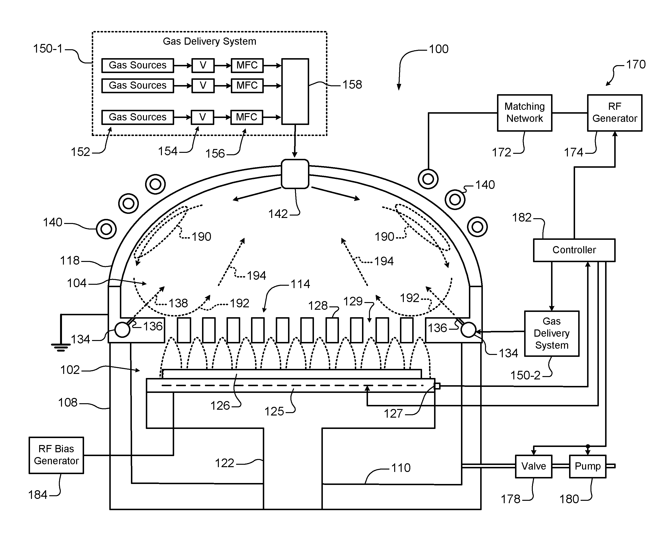
Referring now to FIG. 2, an example of a substrate processing chamber 100 is shown for selectively etching silicon nitride on a substrate and dry cleaning the substrate. The substrate processing chamber 100 includes a lower chamber region 102 and an upper chamber region 104. The lower chamber region 102 is defined by chamber sidewall surfaces 108, a chamber bottom surface 110 and a lower surface of a gas distribution device 114. The upper chamber region 104 is defined by an upper surface of the gas distribution device 114 and an inner surface of a dome 118. In some examples, the dome 118 is spherical, although a cylindrical upper chamber region with a flat top and flat inductive coil(s) can also be used.
A substrate support 122 is arranged in the lower chamber region 104. In some examples, the substrate support 122 includes an electrostatic chuck (ESC), although other types of substrate supports can be used. A substrate 126 is arranged on an upper surface of the substrate support 122 during the etching and dry cleaning process. In some examples, a temperature of the substrate 126 may be controlled by a heater plate 125, an optional cooling plate with flow channels (not shown) and/or one or more sensors 127, although any other suitable substrate heaters may be used.
In some examples, the gas distribution device 114 includes a showerhead (for example, a plate 128 having a plurality of spaced holes 129). The plurality of spaced holes 129 extend from the upper surface of the plate 128 to the lower surface of the plate 128. In some examples, the plurality of holes has a diameter from 0.1'' to 0.75'', although other sizes may be used. In some examples, the plate 128 is made of a conducting material such as aluminum. In other examples, the plate 128 is made of a non-conducting material such as ceramic and includes an embedded electrode.
In some examples, radially outer ends of the gas distribution device 114 may extend upwardly and may define a gas flow channel 134. The gas flow channel 134 is in fluid communication with a plurality of holes 136 for directing gas from the gas flow channel 134 into the upper chamber region 104. In some examples, the plurality of holes 136 direct gas flow from the gas flow channel 134 at an acute radially-inward angle relative to the upper surface of the plate 128 as shown by reference number 138.
An inductive coil 140 is arranged around an outer portion of the dome 118. When energized, the inductive coil 140 creates an electromagnetic field inside of the dome 118. A gas diffuser 142 disburses feed gas or a feed gas mixture from a gas delivery system 150-1. In some examples, the gases may be directed into the upper chamber region using the diffuser 142 and/or the plurality of holes 136.
In some examples, the gas delivery system 150-1 includes one or more gas sources 152, one or more valves 154, one or more mass flow controllers (MFCs) 156, and a mixing manifold 158, although other types of gas delivery systems may be used. Another gas delivery system 150-2 may be used to supply a feed gas or a feed gas mixture to the gas flow channel 134 (in addition to or instead of feed gas from the gas diffuser 142).
A plasma generator 170 may be used to generate RF power that is output to the inductive coil 140. Plasma is generated in the upper chamber region 104. In some examples, the plasma generator 170 includes an RF source 172 and a matching network 174. The matching network 174 matches an impedance of the RF source 172 to the impedance of the inductive coil 140. In some examples, the gas distribution device 114 is grounded. A valve 178 and a pump 180 may be used to control pressure inside of the lower and upper chamber regions 102, 104 and to evacuate reactants from the lower and upper chamber regions 102, 104, respectively.
A controller 176 communicates with the gas delivery systems 150-1 and 150-2, the valve 178, the pump 180, the heater plate 125, and/or the plasma generator 170 to control flow of process gas, purge gas, RF plasma and chamber pressure. Plasma zones 190 are created in the upper chamber region 104. References numbers 190, 192 and 194 illustrate flow of process gases from the gas diffuser 142.
In some examples, plasma is sustained inside the dome 118 by the inductive coil, which is located on an atmospheric side of the dome 118. Feed gas is introduced from the top of the chamber using the gas diffuser 142 and/or the holes 136 and plasma is confined within the dome 118 using the gas distribution device 114, which is grounded. Cold plasma diffuses through the gas distribution device 114 and reacts with the substrate 126 located in the lower chamber region 102.
Confining the plasma in the dome 118 allows volume recombination of plasma species and effusing desired etchant species through the gas distribution device 114. In some examples, there is no bias applied to the substrate 126. As a result, there is no active sheath on the substrate 126 and ions are not hitting the substrate with any finite energy. Some amount of the ions will diffuse out of the plasma region through the gas distribution device 114. However, the amount of plasma that diffuses is an order of magnitude lower than the plasma located inside the dome 118. Most of the ions in the plasma are lost by volume recombination at high pressures. Surface recombination loss at the upper surface of the gas distribution device 114 also lowers ion density below the gas distribution device 114.
In other examples, an RF bias is supplied to the substrate support. An RF bias generator 184 selectively provides an RF bias to the substrate support. A matching network (not shown) may be used between the RF bias generator 184 and the substrate support.
The RF power applied to the inductive coil and the RF bias may have the same or different frequencies or power levels. In some examples, both the RF power applied to the inductive coil and the RF bias are at 13.56 MHz, although other frequencies may be used. For example only, the RF bias may be supplied at a frequency such as 2 MHz, 27 MHz or another frequency while the RF applied to the inductive coil is supplied at a frequency of 13.56 MHz. In some examples, the RF power applied to the inductive coil may be in a range from 1 kW to 5 kW. In other examples, the RF power applied to the inductive coil may be in a range from 1 kW to 2.5 kW. In some examples, the RF bias power may be supplied at a range from 100 W to 1 kW, although other power levels may be used. In some examples, pressure in the processing chamber is in a range from 0.3 Torr to 10 Torr. In other examples, pressure in the processing chamber is in a range from 0.5 Torr to 5 Torr. In some examples, the substrate is maintained at a temperature from 0.degree. C. to 120.degree. C.
Referring now to FIG. 3A, a method 200 for selectively etching silicon nitride is shown. At 204, a substrate is arranged on a substrate support in the lower chamber region. At 208, an etch gas mixture is supplied to the upper chamber region. The etch gas mixture includes one or more gases for promoting silicon nitride etch, passivating polysilicon and passivating silicon dioxide. At 216, plasma is struck in the upper chamber region. In addition, an RF bias may optionally be supplied to the substrate support in the lower chamber region. At 220, the substrate is etched for predetermined period. At 224, the plasma is extinguished after the predetermined period. At 228, a dry clean gas mixture may optionally be supplied to the upper chamber region and plasma may be struck for a predetermined period. The RF bias to the substrate support may be provided during the dry clean process. At 230, the plasma is extinguished after a predetermined period. At 234, the process of etching and dry cleaning may be repeated one or more times in a cyclic manner.
Referring now to FIG. 3B, an alternative process transitions from the silicon nitride etching to the plasma dry cleaning without extinguishing the plasma. At 240, the chemistry is transitioned to a dry clean gas mixture without extinguishing the plasma. The dry clean process proceeds for a predetermined period. The RF bias to the substrate support may be provided during the dry clean process. At 242, the process of etching and dry cleaning may be repeated one or more times in a cyclic manner without extinguishing the plasma. At 244, the plasma is extinguished. Alternately, the plasma may be extinguished when returning to etching and then struck again for etching.
In some examples, gases for promoting nitride etch include nitrogen trifluoride (NF.sub.3), difluoromethane (CH.sub.2F.sub.2), tetrafluoro ethane (CF.sub.4), fluoromethane (CH.sub.3F), a combination of molecular oxygen, molecular nitrogen, and nitrous oxide (O.sub.2/N.sub.2/N.sub.2O), and combinations thereof. In some examples, gases for promoting silicon dioxide passivation include CH.sub.3F, CH.sub.2F.sub.2, and/or O.sub.2/N.sub.2/N.sub.2O. In some examples, gases for promoting polysilicon passivation include O.sub.2/N.sub.2/N.sub.2O, N.sub.2O, or O.sub.2/N.sub.2. In some examples, dry clean gases include carbon dioxide CO.sub.2, carbon dioxide and argon (CO.sub.2/Ar), carbon monoxide (CO), carbon monoxide and argon (CO/Ar) or combinations of the preceding gases, N.sub.2, or N.sub.2O. In some examples, plasma stabilization and dilutive gases may be provided such as argon (Ar).
In some examples, the etch gas mixture includes a nitride etch gas, a polysilicon passivation promoting gas and a silicon dioxide passivation promoting gas. In some examples, the nitride etch gas includes at least one gas selected from a group consisting of NF.sub.3, CH.sub.2F.sub.2, CF.sub.4 and CH.sub.3F and optionally O.sub.2/N.sub.2/N.sub.2O.
In a first example, the etch gas mixture includes NF.sub.3/CH.sub.2F.sub.2/O.sub.2/N.sub.2/N.sub.2O/CO.sub.2. Examples of flow rates are set forth below in Table 1. In this example, NF.sub.3 promotes nitride etch. CH.sub.2F.sub.2 promotes nitride etch and passivates silicon dioxide, O.sub.2/N.sub.2/N.sub.2O promotes nitride etch and promotes polysilicon and silicon dioxide passivation. A dry clean step is performed after the etching process and/or the etching and dry cleaning processes may be performed cyclically.
In a second example, the etch gas mixture includes CF.sub.4/CH.sub.3F/O.sub.2/N.sub.2/N.sub.2O/CO.sub.2. In this example, CF.sub.4 promotes nitride etch. Examples of flow rates are set forth below in Table 1. CH.sub.3F promotes nitride etch and promotes silicon dioxide passivation. O.sub.2/N.sub.2/N.sub.2O promotes nitride etch and promotes polysilicon and silicon dioxide passivation. A plasma dry clean step is performed after the etching process and/or the etching and dry cleaning processes may be performed cyclically.
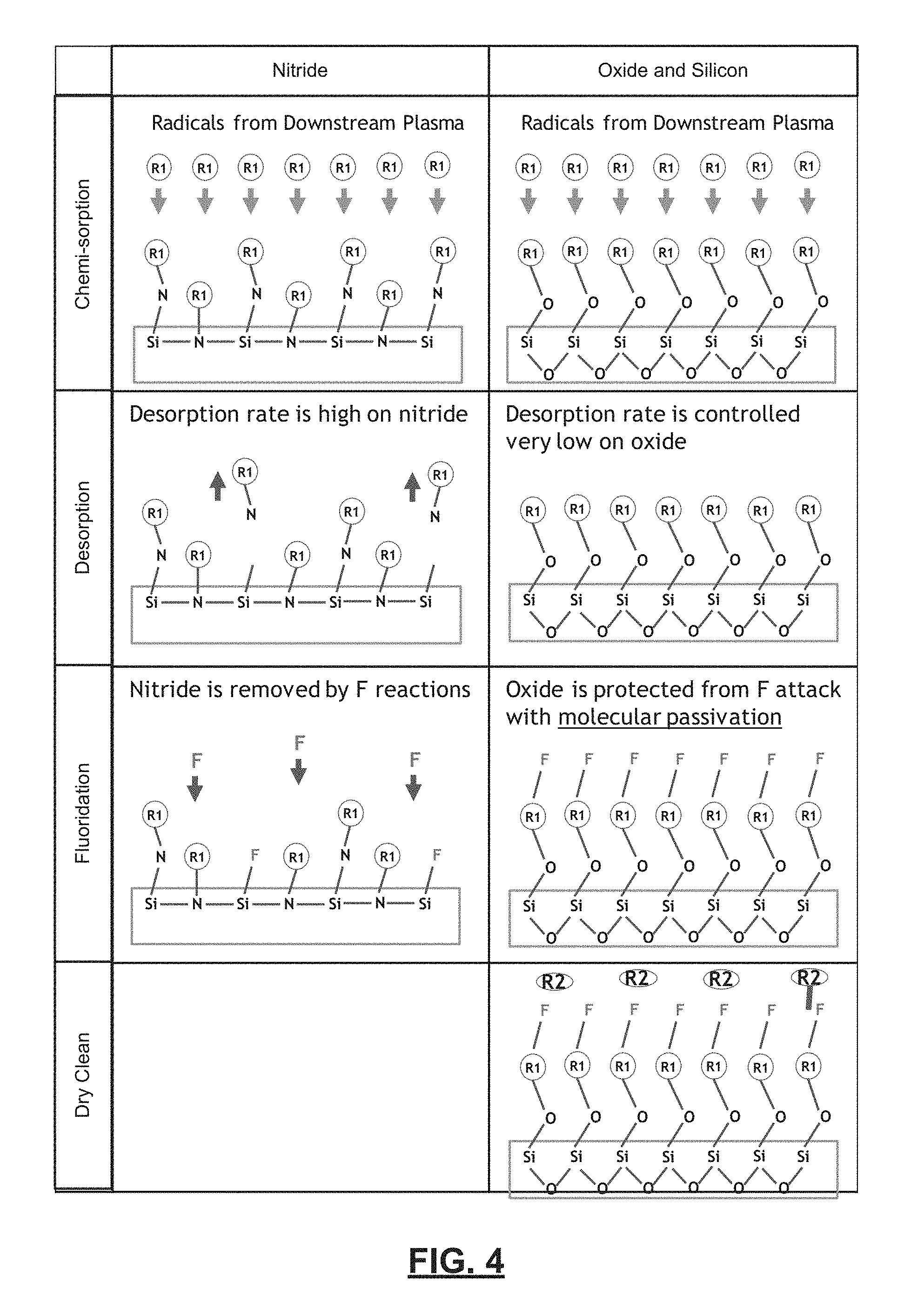
Referring now to FIGS. 4-5, a dry plasma removal process avoids pattern collapsing and provides improved control of top and bottom recess amounts. The systems and methods described herein provide a unique process to passivate surfaces other than nitride with the radical R1. The dry clean or cyclic process removes passivation agents after the etch process or between main etch steps. The inductively coupled plasma source operating at high pressure generates high density of molecular-form radicals R1 in metastable states. The process has increased chemical selectivity for surface passivation as compared to polymer chemistries. Surface passivation can be cleaned up with other radicals such as radical R2.
In FIG. 4, radicals from downstream plasma are chemisorbed by nitride. The desorption rate is high on the silicon nitride. During fluoridation, the silicon nitride is removed by F reactions. Radicals from the downstream plasma are chemisorbed by oxide in the silicon dioxide. The desorption rate is controlled to a very low rate on the oxide. During fluoridation, silicon dioxide is protected from fluorine attack by molecular passivation. In FIG. 5, radicals provided by the dry clean gas remove excess fluorine after etching or between etch steps.
Referring now to FIGS. 6-7, fluorine levels are monitored for the silicon nitride etch without and with the dry clean process described above, respectively. In FIG. 6, a graph illustrates fluorine concentration after the silicon nitride etching without the dry clean process. In FIG. 7, a graph illustrating carbon, nitrogen, oxygen, fluorine and silicon concentrations after using the selective etching and dry clean processes according to the present disclosure are shown.
The selective silicon nitride etch described herein provides high selectivity to polysilicon and silicon dioxide. In some examples, there is no polysilicon loss at bottoms of features and the etch rate is greater than 1000:1. In addition, no pitting was observed. In addition, silicon dioxide selectivity demonstrates less than 1 .ANG. of silicon dioxide thin loss which is greater than 1000:1 selectivity. The fins are sharp and residue free. The selective silicon nitride etch described herein reduces fluorine exposure time by increasing the etch rate. The process uses the radical R2 to eliminate fluorine between, during or after the process. In addition, the process selectively etches silicon nitride relative to other materials such as silicon oxycarbide (SiOC), hafnium oxide (HfO.sub.x) where x is an integer greater than one, titanium nitride (TiN), tantalum nitride (TaN), tungsten (W) and titanium aluminum nitride (TiAlN).
In the following Table 1, typical flow rates for various gases are shown. However, other flow rates may be used.
TABLE-US-00001 TABLE 1 Gas Typical Flow (sccm) Range (sccm) NF.sub.3 100 0-500 CH.sub.2F.sub.2 100 0-500 O.sub.2 3000 1000-5000 N.sub.2 3000 1000-5000 N.sub.2O 4700 1000-8000 CO.sub.2 100 0-500 (ME) 2000 1000-5000 (dry clean) CF.sub.4 100 0-500 CH.sub.3F 100 0-500 CO 2000 1000-5000 (dry clean) Ar 2000 1000-5000 He 2000 1000-5000
The foregoing description is merely illustrative in nature and is in no way intended to limit the disclosure, its application, or uses. The broad teachings of the disclosure can be implemented in a variety of forms. Therefore, while this disclosure includes particular examples, the true scope of the disclosure should not be so limited since other modifications will become apparent upon a study of the drawings, the specification, and the following claims. It should be understood that one or more steps within a method may be executed in different order (or concurrently) without altering the principles of the present disclosure. Further, although each of the embodiments is described above as having certain features, any one or more of those features described with respect to any embodiment of the disclosure can be implemented in and/or combined with features of any of the other embodiments, even if that combination is not explicitly described. In other words, the described embodiments are not mutually exclusive, and permutations of one or more embodiments with one another remain within the scope of this disclosure.
Spatial and functional relationships between elements (for example, between modules, circuit elements, semiconductor layers, etc.) are described using various terms, including "connected," "engaged," "coupled," "adjacent," "next to," "on top of," "above," "below," and "disposed." Unless explicitly described as being "direct," when a relationship between first and second elements is described in the above disclosure, that relationship can be a direct relationship where no other intervening elements are present between the first and second elements, but can also be an indirect relationship where one or more intervening elements are present (either spatially or functionally) between the first and second elements. As used herein, the phrase at least one of A, B, and C should be construed to mean a logical (A OR B OR C), using a non-exclusive logical OR, and should not be construed to mean "at least one of A, at least one of B, and at least one of C."
In some implementations, a controller is part of a system, which may be part of the above-described examples. Such systems can comprise semiconductor processing equipment, including a processing tool or tools, chamber or chambers, a platform or platforms for processing, and/or specific processing components (a wafer pedestal, a gas flow system, etc.). These systems may be integrated with electronics for controlling their operation before, during, and after processing of a semiconductor wafer or substrate. The electronics may be referred to as the "controller," which may control various components or subparts of the system or systems. The controller, depending on the processing requirements and/or the type of system, may be programmed to control any of the processes disclosed herein, including the delivery of processing gases, temperature settings (e.g., heating and/or cooling), pressure settings, vacuum settings, power settings, radio frequency (RF) generator settings, RF matching circuit settings, frequency settings, flow rate settings, fluid delivery settings, positional and operation settings, wafer transfers into and out of a tool and other transfer tools and/or load locks connected to or interfaced with a specific system.
Broadly speaking, the controller may be defined as electronics having various integrated circuits, logic, memory, and/or software that receive instructions, issue instructions, control operation, enable cleaning operations, enable endpoint measurements, and the like. The integrated circuits may include chips in the form of firmware that store program instructions, digital signal processors (DSPs), chips defined as application specific integrated circuits (ASICs), and/or one or more microprocessors, or microcontrollers that execute program instructions (e.g., software). Program instructions may be instructions communicated to the controller in the form of various individual settings (or program files), defining operational parameters for carrying out a particular process on or for a semiconductor wafer or to a system. The operational parameters may, in some embodiments, be part of a recipe defined by process engineers to accomplish one or more processing steps during the fabrication of one or more layers, materials, metals, oxides, silicon, silicon dioxide, surfaces, circuits, and/or dies of a wafer.
The controller, in some implementations, may be a part of or coupled to a computer that is integrated with the system, coupled to the system, otherwise networked to the system, or a combination thereof. For example, the controller may be in the "cloud" or all or a part of a fab host computer system, which can allow for remote access of the wafer processing. The computer may enable remote access to the system to monitor current progress of fabrication operations, examine a history of past fabrication operations, examine trends or performance metrics from a plurality of fabrication operations, to change parameters of current processing, to set processing steps to follow a current processing, or to start a new process. In some examples, a remote computer (e.g. a server) can provide process recipes to a system over a network, which may include a local network or the Internet. The remote computer may include a user interface that enables entry or programming of parameters and/or settings, which are then communicated to the system from the remote computer. In some examples, the controller receives instructions in the form of data, which specify parameters for each of the processing steps to be performed during one or more operations. It should be understood that the parameters may be specific to the type of process to be performed and the type of tool that the controller is configured to interface with or control. Thus as described above, the controller may be distributed, such as by comprising one or more discrete controllers that are networked together and working towards a common purpose, such as the processes and controls described herein. An example of a distributed controller for such purposes would be one or more integrated circuits on a chamber in communication with one or more integrated circuits located remotely (such as at the platform level or as part of a remote computer) that combine to control a process on the chamber.
Without limitation, example systems may include a plasma etch chamber or module, a deposition chamber or module, a spin-rinse chamber or module, a metal plating chamber or module, a clean chamber or module, a bevel edge etch chamber or module, a physical vapor deposition (PVD) chamber or module, a chemical vapor deposition (CVD) chamber or module, an atomic layer deposition (ALD) chamber or module, an atomic layer etch (ALE) chamber or module, an ion implantation chamber or module, a track chamber or module, and any other semiconductor processing systems that may be associated or used in the fabrication and/or manufacturing of semiconductor wafers.
As noted above, depending on the process step or steps to be performed by the tool, the controller might communicate with one or more of other tool circuits or modules, other tool components, cluster tools, other tool interfaces, adjacent tools, neighboring tools, tools located throughout a factory, a main computer, another controller, or tools used in material transport that bring containers of wafers to and from tool locations and/or load ports in a semiconductor manufacturing factory.
* * * * *
D00000
D00001
D00002
D00003
D00004
D00005
D00006
D00007
XML
uspto.report is an independent third-party trademark research tool that is not affiliated, endorsed, or sponsored by the United States Patent and Trademark Office (USPTO) or any other governmental organization. The information provided by uspto.report is based on publicly available data at the time of writing and is intended for informational purposes only.
While we strive to provide accurate and up-to-date information, we do not guarantee the accuracy, completeness, reliability, or suitability of the information displayed on this site. The use of this site is at your own risk. Any reliance you place on such information is therefore strictly at your own risk.
All official trademark data, including owner information, should be verified by visiting the official USPTO website at www.uspto.gov. This site is not intended to replace professional legal advice and should not be used as a substitute for consulting with a legal professional who is knowledgeable about trademark law.