Light-emitting assembly for keyboard
Zercoe , et al. Ja
U.S. patent number 10,192,696 [Application Number 14/867,746] was granted by the patent office on 2019-01-29 for light-emitting assembly for keyboard. This patent grant is currently assigned to APPLE INC.. The grantee listed for this patent is Apple Inc.. Invention is credited to Keith J. Hendren, Craig C. Leong, Bradford J. Zercoe.


| United States Patent | 10,192,696 |
| Zercoe , et al. | January 29, 2019 |
Light-emitting assembly for keyboard
Abstract
A light-emitting assembly positioned within a switch housing of a keyboard assembly for an electronic device is disclosed. The light-emitting assembly may include a phosphor structure, a transparent material positioned on opposing side surfaces of the phosphor structure, and an epoxy layer formed over an entire back surface of the phosphor structure and the transparent material. The light-emitting assembly may also include a mask layer formed over an entire top surface of: the phosphor structure, the transparent material, and the epoxy layer. The light-emitting assembly may further include a light source positioned within the phosphor structure for emitting a light.
| Inventors: | Zercoe; Bradford J. (Cupertino, CA), Leong; Craig C. (Cupertino, CA), Hendren; Keith J. (San Francisco, CA) | ||||||||||
|---|---|---|---|---|---|---|---|---|---|---|---|
| Applicant: |
|
||||||||||
| Assignee: | APPLE INC. (Cupertino,
CA) |
||||||||||
| Family ID: | 54291684 | ||||||||||
| Appl. No.: | 14/867,746 | ||||||||||
| Filed: | September 28, 2015 |
Prior Publication Data
| Document Identifier | Publication Date | |
|---|---|---|
| US 20160093452 A1 | Mar 31, 2016 | |
Related U.S. Patent Documents
| Application Number | Filing Date | Patent Number | Issue Date | ||
|---|---|---|---|---|---|
| 62129842 | Mar 7, 2015 | ||||
| 62129840 | Mar 7, 2015 | ||||
| 62129843 | Mar 7, 2015 | ||||
| 62129841 | Mar 7, 2015 | ||||
| 62058067 | Sep 30, 2014 | ||||
| 62058087 | Sep 30, 2014 | ||||
| 62058081 | Sep 30, 2014 | ||||
| 62058074 | Sep 30, 2014 | ||||
| Current U.S. Class: | 1/1 |
| Current CPC Class: | H01L 33/50 (20130101); H01H 13/7006 (20130101); H01H 13/70 (20130101); H01H 13/06 (20130101); H01H 13/86 (20130101); G06F 3/0202 (20130101); H01H 13/803 (20130101); H01H 13/04 (20130101); G06F 1/1662 (20130101); H01H 13/79 (20130101); H01H 13/80 (20130101); H01H 3/125 (20130101); H01H 13/023 (20130101); H01H 13/83 (20130101); H01H 2205/016 (20130101); H01H 2203/056 (20130101); H01H 2229/046 (20130101); H01H 2203/038 (20130101); H01H 2213/016 (20130101); H01H 2211/028 (20130101); H01H 2207/04 (20130101); H01H 2203/004 (20130101); H01H 2219/052 (20130101); H01H 2213/01 (20130101); H01H 2215/038 (20130101); H01H 2221/076 (20130101); H01H 2205/024 (20130101); H01H 2227/026 (20130101); H01H 2219/036 (20130101); H01H 2219/062 (20130101); H01H 2239/004 (20130101); H01H 2219/06 (20130101) |
| Current International Class: | H01H 13/83 (20060101); H01H 13/80 (20060101); H01H 13/803 (20060101); H01H 13/86 (20060101); H01H 13/04 (20060101); H01H 13/02 (20060101); H01H 13/79 (20060101); H01H 3/12 (20060101); G06F 3/02 (20060101); G06F 1/16 (20060101); H01H 13/06 (20060101); H01L 33/50 (20100101); H01H 13/70 (20060101) |
| Field of Search: | ;200/310-314,317 |
References Cited [Referenced By]
U.S. Patent Documents
| 3657492 | April 1972 | Arndt et al. |
| 3917917 | November 1975 | Murata |
| 3978297 | August 1976 | Lynn et al. |
| 4095066 | June 1978 | Harris |
| 4319099 | March 1982 | Asher |
| 4349712 | September 1982 | Michalski |
| 4484042 | November 1984 | Matsui |
| 4596905 | June 1986 | Fowler |
| 4598181 | July 1986 | Selby |
| 4670084 | June 1987 | Durand et al. |
| 4755645 | July 1988 | Naoki et al. |
| 4937408 | June 1990 | Hattori et al. |
| 4987275 | January 1991 | Miller et al. |
| 5021638 | June 1991 | Nopper et al. |
| 5092459 | March 1992 | Uljanic et al. |
| 5136131 | August 1992 | Komaki |
| 5278372 | January 1994 | Takagi et al. |
| 5280146 | January 1994 | Inagaki et al. |
| 5340955 | August 1994 | Calvillo et al. |
| 5382762 | January 1995 | Mochizuki |
| 5397867 | March 1995 | Demeo |
| 5408060 | April 1995 | Muurinen |
| 5421659 | June 1995 | Liang |
| 5422447 | June 1995 | Spence |
| 5457297 | October 1995 | Chen |
| 5477430 | December 1995 | Larose |
| 5481074 | January 1996 | English |
| 5504283 | April 1996 | Kako et al. |
| 5512719 | April 1996 | Okada et al. |
| 5625532 | April 1997 | Sellers |
| 5804780 | September 1998 | Bartha |
| 5828015 | October 1998 | Coulon |
| 5847337 | December 1998 | Chen |
| 5874700 | February 1999 | Hochgesang |
| 5875013 | February 1999 | Takahara |
| 5876106 | March 1999 | Kordecki |
| 5878872 | March 1999 | Tsai |
| 5881866 | March 1999 | Miyajima et al. |
| 5898147 | April 1999 | Domzaiski et al. |
| 5924555 | July 1999 | Sadamori et al. |
| 5935691 | August 1999 | Tsai |
| 5960942 | October 1999 | Thornton |
| 5986227 | November 1999 | Hon |
| 6020565 | February 2000 | Pan |
| 6068416 | May 2000 | Kumamoto et al. |
| 6215420 | April 2001 | Harrison et al. |
| 6257782 | July 2001 | Maruyama et al. |
| 6259046 | July 2001 | Iwama et al. |
| 6377685 | April 2002 | Krishnan |
| 6388219 | May 2002 | Hsu et al. |
| 6423918 | July 2002 | King et al. |
| 6482032 | November 2002 | Szu et al. |
| 6530283 | March 2003 | Okada et al. |
| 6538801 | March 2003 | Jacobson et al. |
| 6542355 | April 2003 | Huang |
| 6552287 | April 2003 | Janniere |
| 6556112 | April 2003 | Van Zeeland et al. |
| 6559399 | May 2003 | Hsu et al. |
| 6560612 | May 2003 | Yamada et al. |
| 6572289 | June 2003 | Lo et al. |
| 6573463 | June 2003 | Ono |
| 6585435 | July 2003 | Fang |
| 6624369 | September 2003 | Ito et al. |
| 6706986 | March 2004 | Hsu |
| 6738050 | May 2004 | Comiskey |
| 6750414 | June 2004 | Sullivan |
| 6759614 | July 2004 | Yoneyama |
| 6762381 | July 2004 | Kunthady et al. |
| 6765503 | July 2004 | Chan |
| 6788450 | September 2004 | Kawai et al. |
| 6797906 | September 2004 | Ohashi |
| 6850227 | February 2005 | Takahashi et al. |
| 6860660 | March 2005 | Hochgesang et al. |
| 6911608 | June 2005 | Levy |
| 6926418 | August 2005 | Ostergard et al. |
| 6940030 | September 2005 | Takeda et al. |
| 6977352 | December 2005 | Oosawa |
| 6979792 | December 2005 | Lai |
| 6987466 | January 2006 | Welch et al. |
| 6987503 | January 2006 | Inoue |
| 7012206 | March 2006 | Oikawa |
| 7030330 | April 2006 | Suda |
| 7038832 | May 2006 | Kanbe |
| 7129930 | October 2006 | Cathey et al. |
| 7134205 | November 2006 | Bruennel |
| 7146701 | December 2006 | Mahoney et al. |
| 7151236 | December 2006 | Ducruet et al. |
| 7151237 | December 2006 | Mahoney et al. |
| 7154059 | December 2006 | Chou |
| 7166813 | January 2007 | Soma |
| 7172303 | February 2007 | Shipman et al. |
| 7189932 | March 2007 | Kim |
| 7256766 | August 2007 | Albert et al. |
| 7283119 | October 2007 | Kishi |
| 7301113 | November 2007 | Nishimura et al. |
| 7312790 | December 2007 | Sato et al. |
| 7378607 | May 2008 | Koyano et al. |
| 7385806 | June 2008 | Liao |
| 7391555 | June 2008 | Albert et al. |
| 7414213 | August 2008 | Hwang |
| 7429707 | September 2008 | Yanai et al. |
| 7432460 | October 2008 | Clegg |
| 7510342 | March 2009 | Lane et al. |
| 7531764 | May 2009 | Lev et al. |
| 7541554 | June 2009 | Hou |
| 7589292 | September 2009 | Jung et al. |
| 7639187 | December 2009 | Caballero et al. |
| 7639571 | December 2009 | Ishii et al. |
| 7651231 | January 2010 | Chou |
| 7679010 | March 2010 | Wingett |
| 7724415 | May 2010 | Yamaguchi |
| 7781690 | August 2010 | Ishii |
| 7813774 | October 2010 | Perez-Noguera |
| 7842895 | November 2010 | Lee |
| 7847204 | December 2010 | Tsai |
| 7851819 | December 2010 | Shi |
| 7866866 | January 2011 | Wahlstrom |
| 7893376 | February 2011 | Chen |
| 7923653 | April 2011 | Ohsumi |
| 7947915 | May 2011 | Lee et al. |
| 7999748 | August 2011 | Ligtenberg et al. |
| 8063325 | November 2011 | Sung et al. |
| 8077096 | December 2011 | Chiang et al. |
| 8080744 | December 2011 | Yeh et al. |
| 8098228 | January 2012 | Shimodaira et al. |
| 8109650 | February 2012 | Chang et al. |
| 8119945 | February 2012 | Lin |
| 8124903 | February 2012 | Tatehata et al. |
| 8134094 | March 2012 | Tsao et al. |
| 8143982 | March 2012 | Lauder et al. |
| 8156172 | April 2012 | Muehl et al. |
| 8178808 | May 2012 | Strittmatter et al. |
| 8184021 | May 2012 | Chou |
| 8212160 | July 2012 | Tsao |
| 8212162 | July 2012 | Zhou |
| 8218301 | July 2012 | Lee |
| 8232958 | July 2012 | Tolbert |
| 8246228 | August 2012 | Ko et al. |
| 8253048 | August 2012 | Ozias et al. |
| 8253052 | September 2012 | Chen |
| 8263887 | September 2012 | Chen et al. |
| 8289280 | October 2012 | Travis |
| 8299382 | October 2012 | Takemae et al. |
| 8317384 | November 2012 | Chung et al. |
| 8319298 | November 2012 | Hsu |
| 8325141 | December 2012 | Marsden |
| 8330725 | December 2012 | Mahowald et al. |
| 8354629 | January 2013 | Lin |
| 8378857 | February 2013 | Pance |
| 8383972 | February 2013 | Liu |
| 8384566 | February 2013 | Bocirnea |
| 8404990 | March 2013 | Lutgring et al. |
| 8451146 | March 2013 | Mahowald et al. |
| 8431849 | April 2013 | Chen |
| 8436265 | May 2013 | Koike et al. |
| 8462514 | June 2013 | Myers et al. |
| 8500348 | August 2013 | Dumont et al. |
| 8502094 | August 2013 | Chen |
| 8542194 | September 2013 | Akens et al. |
| 8548528 | October 2013 | Kim et al. |
| 8564544 | October 2013 | Jobs et al. |
| 8569639 | October 2013 | Strittmatter |
| 8575632 | November 2013 | Kuramoto |
| 8581127 | November 2013 | Jhuang et al. |
| 8592699 | November 2013 | Kessler et al. |
| 8592702 | November 2013 | Tsai |
| 8592703 | November 2013 | Johnson et al. |
| 8604370 | December 2013 | Chao |
| 8629362 | January 2014 | Knighton et al. |
| 8642904 | February 2014 | Chiba et al. |
| 8651720 | February 2014 | Sherman et al. |
| 8659882 | February 2014 | Liang et al. |
| 8731618 | May 2014 | Jarvis et al. |
| 8748767 | June 2014 | Ozias et al. |
| 8759705 | June 2014 | Funakoshi et al. |
| 8760405 | June 2014 | Nam |
| 8786548 | July 2014 | Oh et al. |
| 8791378 | July 2014 | Lan |
| 8835784 | September 2014 | Hirota |
| 8847090 | September 2014 | Ozaki |
| 8847711 | September 2014 | Yang et al. |
| 8853580 | October 2014 | Chen |
| 8854312 | October 2014 | Meierling |
| 8870477 | October 2014 | Merminod et al. |
| 8884174 | November 2014 | Chou et al. |
| 8921473 | December 2014 | Hyman |
| 8922476 | December 2014 | Stewart et al. |
| 8943427 | January 2015 | Heo et al. |
| 8976117 | March 2015 | Krahenbuhl et al. |
| 8994641 | March 2015 | Stewart et al. |
| 9007297 | April 2015 | Stewart et al. |
| 9012795 | April 2015 | Niu et al. |
| 9029723 | May 2015 | Pegg |
| 9063627 | June 2015 | Yairi et al. |
| 9064642 | June 2015 | Welch et al. |
| 9086733 | July 2015 | Pance |
| 9087663 | July 2015 | Los |
| 9093229 | July 2015 | Leong et al. |
| 9213416 | December 2015 | Chen |
| 9223352 | December 2015 | Smith et al. |
| 9234486 | January 2016 | Das et al. |
| 9235236 | January 2016 | Nam |
| 9274654 | March 2016 | Slobodin et al. |
| 9275810 | March 2016 | Pance et al. |
| 9300033 | March 2016 | Han et al. |
| 9305496 | April 2016 | Kimura |
| 9443672 | September 2016 | Martisauskas |
| 9448628 | September 2016 | Tan et al. |
| 9471185 | October 2016 | Guard |
| 9477382 | October 2016 | Hicks et al. |
| 9612674 | April 2017 | Degner et al. |
| 9734965 | August 2017 | Martinez et al. |
| 9793066 | October 2017 | Brock et al. |
| 2002/0079211 | June 2002 | Katayama et al. |
| 2002/0093436 | July 2002 | Lien |
| 2002/0113770 | August 2002 | Jacobson et al. |
| 2002/0149835 | October 2002 | Kanbe |
| 2003/0169232 | September 2003 | Ito |
| 2004/0004559 | January 2004 | Rast |
| 2004/0225965 | November 2004 | Garside et al. |
| 2004/0257247 | December 2004 | Lin et al. |
| 2005/0035950 | February 2005 | Daniels |
| 2005/0253801 | November 2005 | Kobayashi |
| 2006/0011458 | January 2006 | Purcocks |
| 2006/0020469 | January 2006 | Rast |
| 2006/0120790 | June 2006 | Chang |
| 2006/0181511 | August 2006 | Woolley |
| 2006/0243987 | November 2006 | Lai |
| 2007/0200823 | August 2007 | Bytheway et al. |
| 2007/0285393 | December 2007 | Ishakov |
| 2008/0131184 | June 2008 | Brown et al. |
| 2008/0136782 | June 2008 | Mundt et al. |
| 2008/0251370 | October 2008 | Aoki |
| 2009/0046053 | February 2009 | Shigehiro et al. |
| 2009/0103964 | April 2009 | Takagi et al. |
| 2009/0128496 | May 2009 | Huang |
| 2009/0262085 | October 2009 | Wassingbo et al. |
| 2009/0267892 | October 2009 | Faubert |
| 2010/0045705 | February 2010 | Vertegaal et al. |
| 2010/0066568 | March 2010 | Lee |
| 2010/0109921 | May 2010 | Annerfors |
| 2010/0156796 | June 2010 | Kim et al. |
| 2010/0253630 | October 2010 | Homma et al. |
| 2011/0032127 | February 2011 | Roush |
| 2011/0056817 | March 2011 | Wu |
| 2011/0056836 | March 2011 | Tatebe et al. |
| 2011/0205179 | August 2011 | Braun |
| 2011/0261031 | October 2011 | Muto |
| 2011/0267272 | November 2011 | Meyer et al. |
| 2011/0284355 | November 2011 | Yang |
| 2011/0303521 | December 2011 | Niu et al. |
| 2012/0012446 | January 2012 | Hwa |
| 2012/0032972 | February 2012 | Hwang |
| 2012/0090973 | April 2012 | Liu |
| 2012/0098751 | April 2012 | Liu |
| 2012/0286701 | November 2012 | Yang et al. |
| 2012/0298496 | November 2012 | Zhang |
| 2012/0313856 | December 2012 | Hsieh |
| 2013/0043115 | February 2013 | Yang et al. |
| 2013/0093500 | April 2013 | Bruwer |
| 2013/0093733 | April 2013 | Yoshida |
| 2013/0100030 | April 2013 | Los et al. |
| 2013/0120265 | May 2013 | Horii et al. |
| 2013/0161170 | June 2013 | Fan |
| 2013/0215079 | August 2013 | Johnson et al. |
| 2013/0242601 | September 2013 | Kloeppel et al. |
| 2013/0270090 | October 2013 | Lee |
| 2014/0015777 | January 2014 | Park et al. |
| 2014/0027259 | January 2014 | Kawana et al. |
| 2014/0071654 | March 2014 | Chien |
| 2014/0082490 | March 2014 | Jung et al. |
| 2014/0090967 | April 2014 | Inagaki |
| 2014/0098042 | April 2014 | Kuo et al. |
| 2014/0116865 | May 2014 | Leong et al. |
| 2014/0118264 | May 2014 | Leong et al. |
| 2014/0151211 | June 2014 | Zhang |
| 2014/0184496 | July 2014 | Gribetz et al. |
| 2014/0191973 | July 2014 | Zellers et al. |
| 2014/0218851 | August 2014 | Klein et al. |
| 2014/0252881 | September 2014 | Dinh et al. |
| 2014/0291133 | October 2014 | Fu et al. |
| 2014/0320436 | October 2014 | Modarres et al. |
| 2014/0346025 | November 2014 | Hendren et al. |
| 2014/0375141 | December 2014 | Nakajima |
| 2015/0016038 | January 2015 | Niu et al. |
| 2015/0083561 | March 2015 | Han et al. |
| 2015/0090570 | April 2015 | Kwan et al. |
| 2015/0090571 | April 2015 | Leong et al. |
| 2015/0227207 | August 2015 | Winter et al. |
| 2015/0243457 | August 2015 | Niu et al. |
| 2015/0270073 | September 2015 | Yarak, III et al. |
| 2015/0277559 | October 2015 | Vescovi et al. |
| 2015/0287553 | October 2015 | Welch et al. |
| 2015/0309538 | October 2015 | Zhang |
| 2015/0332874 | November 2015 | Brock et al. |
| 2015/0348726 | December 2015 | Hendren |
| 2015/0378391 | December 2015 | Huitema et al. |
| 2016/0049266 | February 2016 | Stringer et al. |
| 2016/0172129 | June 2016 | Zercoe et al. |
| 2016/0189890 | June 2016 | Leong et al. |
| 2016/0189891 | June 2016 | Zercoe et al. |
| 2016/0259375 | September 2016 | Andre et al. |
| 2016/0329166 | November 2016 | Hou et al. |
| 2016/0336124 | November 2016 | Leong et al. |
| 2016/0336127 | November 2016 | Leong et al. |
| 2016/0336128 | November 2016 | Leong et al. |
| 2016/0343523 | November 2016 | Hendren et al. |
| 2016/0351360 | December 2016 | Knopf et al. |
| 2016/0365204 | December 2016 | Cao et al. |
| 2016/0378234 | December 2016 | Ligtenberg et al. |
| 2016/0379775 | December 2016 | Leong et al. |
| 2017/0004937 | January 2017 | Leong et al. |
| 2017/0004939 | January 2017 | Kwan et al. |
| 2017/0011869 | January 2017 | Knopf et al. |
| 2017/0090106 | March 2017 | Cao et al. |
| 2017/0301487 | October 2017 | Leong et al. |
| 2017/0315624 | November 2017 | Leong et al. |
| 2018/0029339 | February 2018 | Liu et al. |
| 2018/0040441 | February 2018 | Wu et al. |
| 2018/0074694 | March 2018 | Lehmann et al. |
| 2155620 | Feb 1994 | CN | |||
| 2394309 | Aug 2000 | CN | |||
| 1533128 | Sep 2004 | CN | |||
| 1542497 | Nov 2004 | CN | |||
| 2672832 | Jan 2005 | CN | |||
| 1624842 | Jun 2005 | CN | |||
| 1812030 | Aug 2006 | CN | |||
| 1838036 | Sep 2006 | CN | |||
| 1855332 | Nov 2006 | CN | |||
| 101051569 | Oct 2007 | CN | |||
| 200961844 | Oct 2007 | CN | |||
| 200986871 | Dec 2007 | CN | |||
| 101146137 | Mar 2008 | CN | |||
| 201054315 | Apr 2008 | CN | |||
| 201084602 | Jul 2008 | CN | |||
| 201123174 | Sep 2008 | CN | |||
| 201149829 | Nov 2008 | CN | |||
| 101315841 | Dec 2008 | CN | |||
| 201210457 | Mar 2009 | CN | |||
| 101438228 | May 2009 | CN | |||
| 101465226 | Jun 2009 | CN | |||
| 101494130 | Jul 2009 | CN | |||
| 101502082 | Aug 2009 | CN | |||
| 201298481 | Aug 2009 | CN | |||
| 101546667 | Sep 2009 | CN | |||
| 101572195 | Nov 2009 | CN | |||
| 101800281 | Aug 2010 | CN | |||
| 101807482 | Aug 2010 | CN | |||
| 101868773 | Oct 2010 | CN | |||
| 201655616 | Nov 2010 | CN | |||
| 102110542 | Jun 2011 | CN | |||
| 102119430 | Jul 2011 | CN | |||
| 201904256 | Jul 2011 | CN | |||
| 102163084 | Aug 2011 | CN | |||
| 201927524 | Aug 2011 | CN | |||
| 201945951 | Aug 2011 | CN | |||
| 201945952 | Aug 2011 | CN | |||
| 201956238 | Aug 2011 | CN | |||
| 102197452 | Sep 2011 | CN | |||
| 202008941 | Oct 2011 | CN | |||
| 202040690 | Nov 2011 | CN | |||
| 102280292 | Dec 2011 | CN | |||
| 102338348 | Feb 2012 | CN | |||
| 102375550 | Mar 2012 | CN | |||
| 202205161 | Apr 2012 | CN | |||
| 102496509 | Jun 2012 | CN | |||
| 10269527 | Aug 2012 | CN | |||
| 102622089 | Aug 2012 | CN | |||
| 102629526 | Aug 2012 | CN | |||
| 202372927 | Aug 2012 | CN | |||
| 102679239 | Sep 2012 | CN | |||
| 102683072 | Sep 2012 | CN | |||
| 202434387 | Sep 2012 | CN | |||
| 202523007 | Nov 2012 | CN | |||
| 102832068 | Dec 2012 | CN | |||
| 102955573 | Mar 2013 | CN | |||
| 102956386 | Mar 2013 | CN | |||
| 102969183 | Mar 2013 | CN | |||
| 103000417 | Mar 2013 | CN | |||
| 103165327 | Jun 2013 | CN | |||
| 103180979 | Jun 2013 | CN | |||
| 203012648 | Jun 2013 | CN | |||
| 203135988 | Aug 2013 | CN | |||
| 103377841 | Oct 2013 | CN | |||
| 103489986 | Jan 2014 | CN | |||
| 203414880 | Jan 2014 | CN | |||
| 103681056 | Mar 2014 | CN | |||
| 103699181 | Apr 2014 | CN | |||
| 203520312 | Apr 2014 | CN | |||
| 203588895 | May 2014 | CN | |||
| 103839715 | Jun 2014 | CN | |||
| 103839720 | Jun 2014 | CN | |||
| 103839722 | Jun 2014 | CN | |||
| 103903891 | Jul 2014 | CN | |||
| 103956290 | Jul 2014 | CN | |||
| 203733685 | Jul 2014 | CN | |||
| 104021968 | Sep 2014 | CN | |||
| 204102769 | Jan 2015 | CN | |||
| 204117915 | Jan 2015 | CN | |||
| 104517769 | Apr 2015 | CN | |||
| 204632641 | Sep 2015 | CN | |||
| 105097341 | Nov 2015 | CN | |||
| 2530176 | Jan 1977 | DE | |||
| 3002772 | Jul 1981 | DE | |||
| 29704100 | Apr 1997 | DE | |||
| 202008001970 | Aug 2008 | DE | |||
| 0441993 | Aug 1991 | EP | |||
| 1835272 | Sep 2007 | EP | |||
| 1928008 | Jun 2008 | EP | |||
| 2022606 | Jun 2010 | EP | |||
| 2426688 | Mar 2012 | EP | |||
| 2439760 | Apr 2012 | EP | |||
| 2463798 | Jun 2012 | EP | |||
| 2664979 | Nov 2013 | EP | |||
| 2147420 | Mar 1973 | FR | |||
| 2911000 | Jul 2008 | FR | |||
| 2950193 | Mar 2011 | FR | |||
| 1361459 | Jul 1974 | GB | |||
| S50115562 | Sep 1975 | JP | |||
| S60055477 | Mar 1985 | JP | |||
| S61172422 | Oct 1986 | JP | |||
| S62072429 | Apr 1987 | JP | |||
| S63182024 | Nov 1988 | JP | |||
| H0422024 | Apr 1992 | JP | |||
| H0520963 | Jan 1993 | JP | |||
| H0524512 | Aug 1993 | JP | |||
| H05342944 | Dec 1993 | JP | |||
| H09204148 | Aug 1997 | JP | |||
| H10312726 | Nov 1998 | JP | |||
| H11194882 | Jul 1999 | JP | |||
| 2000010709 | Jan 2000 | JP | |||
| 2000057871 | Feb 2000 | JP | |||
| 2000339097 | Dec 2000 | JP | |||
| 2001100889 | Apr 2001 | JP | |||
| 2003114751 | Sep 2001 | JP | |||
| 2002260478 | Sep 2002 | JP | |||
| 2002298689 | Oct 2002 | JP | |||
| 2003522998 | Jul 2003 | JP | |||
| 2005108041 | Apr 2005 | JP | |||
| 2006164929 | Jun 2006 | JP | |||
| 2006185906 | Jul 2006 | JP | |||
| 2006521664 | Sep 2006 | JP | |||
| 2006269439 | Oct 2006 | JP | |||
| 2006277013 | Oct 2006 | JP | |||
| 2006344609 | Dec 2006 | JP | |||
| 2007115633 | May 2007 | JP | |||
| 2007514247 | May 2007 | JP | |||
| 2007156983 | Jun 2007 | JP | |||
| 2008021428 | Jan 2008 | JP | |||
| 2008041431 | Feb 2008 | JP | |||
| 2008100129 | May 2008 | JP | |||
| 2008191850 | Aug 2008 | JP | |||
| 2008533559 | Aug 2008 | JP | |||
| 2008293922 | Dec 2008 | JP | |||
| 2009099503 | May 2009 | JP | |||
| 2009181894 | Aug 2009 | JP | |||
| 2010061956 | Mar 2010 | JP | |||
| 2010244088 | Oct 2010 | JP | |||
| 2010244302 | Oct 2010 | JP | |||
| 2011018484 | Jan 2011 | JP | |||
| 2011065126 | Mar 2011 | JP | |||
| 2011150804 | Aug 2011 | JP | |||
| 2011165630 | Aug 2011 | JP | |||
| 2011524066 | Aug 2011 | JP | |||
| 2011187297 | Sep 2011 | JP | |||
| 2012022473 | Feb 2012 | JP | |||
| 2012043705 | Mar 2012 | JP | |||
| 2012063630 | Mar 2012 | JP | |||
| 2012098873 | May 2012 | JP | |||
| 2012134064 | Jul 2012 | JP | |||
| 2012186067 | Sep 2012 | JP | |||
| 2012230256 | Nov 2012 | JP | |||
| 2014017179 | Jan 2014 | JP | |||
| 2014026807 | Feb 2014 | JP | |||
| 2014216190 | Nov 2014 | JP | |||
| 2014220039 | Nov 2014 | JP | |||
| 2016053778 | Apr 2016 | JP | |||
| 1019990007394 | Jan 1999 | KR | |||
| 1020020001668 | Jan 2002 | KR | |||
| 100454203 | Oct 2004 | KR | |||
| 1020060083032 | Jul 2006 | KR | |||
| 1020080064116 | Jul 2008 | KR | |||
| 1020080066164 | Jul 2008 | KR | |||
| 2020110006385 | Jun 2011 | KR | |||
| 1020120062797 | Jun 2012 | KR | |||
| 1020130040131 | Apr 2013 | KR | |||
| 20150024201 | Mar 2015 | KR | |||
| 200703396 | Jan 2007 | TW | |||
| M334397 | Jun 2008 | TW | |||
| 201108284 | Mar 2011 | TW | |||
| 201108286 | Mar 2011 | TW | |||
| M407429 | Jul 2011 | TW | |||
| 201246251 | Nov 2012 | TW | |||
| 201403646 | Jan 2014 | TW | |||
| WO9744946 | Nov 1997 | WO | |||
| WO2005/057320 | Jun 2005 | WO | |||
| WO2006/022313 | Mar 2006 | WO | |||
| WO2007/049253 | May 2007 | WO | |||
| WO2008/045833 | Apr 2008 | WO | |||
| WO2009/005026 | Jan 2009 | WO | |||
| WO2012/011282 | Jan 2012 | WO | |||
| WO2012/027978 | Mar 2012 | WO | |||
| WO2013/096478 | Jun 2013 | WO | |||
| WO2014175446 | Oct 2014 | WO | |||
Other References
|
Elekson, "Reliable and Tested Wearable Electronics Embedment Solutions," http://www.wearable.technology/our-technologies, 3 pages, at least as early as Jan. 6, 2016. cited by applicant . U.S. Appl. No. 14/472,260, filed Aug. 28, 2014, pending. cited by applicant . U.S. Appl. No. 14/501,680, filed Sep. 30, 2014, pending. cited by applicant . U.S. Appl. No. 14/736,151, filed Jun. 10, 2015, pending. cited by applicant . U.S. Appl. No. 14/765,145, filed Jul. 31, 2015, pending. cited by applicant . U.S. Appl. No. 14/826,590, filed Aug. 14, 2015, pending. cited by applicant . U.S. Appl. No. 14/867,598, filed Sep. 28, 2015, pending. cited by applicant . U.S. Appl. No. 14/867,672, filed Sep. 28, 2015, pending. cited by applicant . U.S. Appl. No. 14/867,712, filed Sep. 28, 2015, pending. cited by applicant. |
Primary Examiner: Leon; Edwin A.
Assistant Examiner: Caroc; Lheiren Mae A
Attorney, Agent or Firm: Dorsey & Whitney LLP
Parent Case Text
CROSS-REFERENCE TO RELATED APPLICATIONS
This application is a non-provisional patent application of and claims the benefit to U.S. Provisional Patent Application No. 62/058,081, filed Sep. 30, 2014, and titled "Keyboard Assembly," U.S. Provisional Patent Application No. 62/129,843, filed Mar. 7, 2015, and titled "Light Assembly for Keyboard Assembly," U.S. Provisional Patent Application No. 62/058,074, filed Sep. 30, 2014, and titled "Keyboard Assembly," U.S. Provisional Patent Application No. 62/129,841, filed Mar. 7, 2015, and titled "Key for Keyboard Assembly," U.S. Provisional Patent Application No. 62/058,067, filed Sep. 30, 2014 and titled "Keyboard Assembly," U.S. Provisional Patent Application No. 62/129,840, filed Mar. 7, 2015, and titled "Dome Switch for Keyboard Assembly," U.S. Provisional Patent Application No. 62/058,087, filed Sep. 30, 2014, and titled "Keyboard Assembly," and U.S. Provisional Patent Application No. 62/129,842, filed Mar. 7, 2015, and titled "Venting System for Keyboard Assembly," the disclosures of which are hereby incorporated herein by reference in their entirety.
Claims
What is claimed is:
1. A keyboard assembly, comprising: a switch housing defining a switch opening and a light source recess formed in a sidewall of the switch opening; a tactile dome positioned at least partially within the switch opening; a keycap positioned above the switch housing and configured to move toward the tactile dome when pressed; and a light-emitting assembly positioned within the light source recess of the switch housing, and comprising: a light source; a luminescent structure at least partially enclosing the light source and defining a front face of the light-emitting assembly; an opaque material defining a rear face of the light-emitting assembly, the rear face being positioned opposite the front face; a first sidewall defining a first side face of the light-emitting assembly; and a second sidewall opposite the first sidewall and defining a second side face of the light-emitting assembly, wherein the switch housing is configured to receive light from each of the front face, the first side face, and the second side face and to guide the received light toward the keycap, wherein the opaque material is configured to prevent light from passing through it.
2. The keyboard assembly of claim 1, wherein the luminescent structure is formed from a phosphor material.
3. The keyboard assembly of claim 1, wherein: the switch housing is formed from a substantially transparent material; and the light source is configured to emit light through the substantially transparent material of the switch housing.
4. The keyboard assembly of claim 1, wherein the keycap includes a transparent glyph formed through the keycap.
5. The keyboard assembly of claim 4, wherein the light source emits light to at least one of: a perimeter of the keycap; and the transparent glyph formed through the keycap.
6. The keyboard assembly of claim 1, wherein the light-emitting assembly is substantially surrounded on three sides by sidewalls of the light source recess.
7. The keyboard assembly of claim 6, further comprising a transparent resin positioned over the light-emitting assembly, between the light-emitting assembly and the sidewalls of the light source recess.
8. A method for illuminating a key cap, comprising: activating a light source; transmitting light from the light source, through a phosphor structure, and into a switch housing into three distinct surfaces of the switch housing; redirecting, through the switch housing, the light from the phosphor structure to an underside of the key cap, thereby illuminating a portion of the key cap; and blocking at least a portion of the light that is emitted through the phosphor structure and upward toward the key cap; blocking at least a portion of the light that is laterally emitted through the phosphor structure opposite at least one of the three distinct surfaces of the switch housing.
9. The method of claim 8, further comprising shifting a color of the light while the light transmits through the phosphor structure.
10. The keyboard assembly of claim 1, further comprising an optical mask positioned at least partially between the light source and an underside of the key cap.
11. A keyboard assembly, comprising: a key cap; a tactile switch positioned below the key cap; a support structure movably supporting the key cap; a switch housing positioned below the key cap and defining an opening that surrounds the tactile switch and a recess; and a light-emitting assembly positioned at least partially within the recess and configured to direct light into the switch housing along three directions, wherein the switch housing defines a light guide configured to channel light received from the light-emitting assembly toward an underside of the key cap; an opaque material positioned on a side of the light-emitting assembly and configured to at least partially block light from exiting the light-emitting assembly along a fourth direction, the fourth direction being opposite one of the three directions.
12. The keyboard assembly of claim 11, further comprising an optical mask positioned at least partially between the light emitting assembly and the underside of the key cap.
13. The keyboard assembly of claim 11, wherein the light-emitting assembly further comprises a phosphor structure at least partially surrounding a light source; the light-emitting assembly defines a front face and two side faces adjoining the front face; the light is coupled into the switch housing from the front face and the two side faces of the light-emitting assembly.
14. The keyboard assembly of claim 13, wherein the light-emitting assembly further comprises: a first transparent sidewall extending from a first end of the front face and defines a first of the two side faces; and a second transparent sidewall extending from a second end of the front face defines a second of the two side faces.
15. The keyboard assembly of claim, 13, wherein the light source is embedded within the phosphor structure.
16. The keyboard assembly of claim 11, wherein: the key cap defines an illuminable symbol; and the switch housing is configured to illuminate the illuminable symbol by propagating light received from the light-emitting assembly toward the underside of the key cap.
17. The keyboard assembly of claim 11, wherein: the switch housing propagates light toward the underside of the key cap through the opening.
18. The keyboard assembly of claim 11, further comprising: a top panel positioned over the opening and between the tactile switch and the key cap.
19. The keyboard assembly of claim 18, wherein the top panel defines a light guide.
20. The keyboard assembly of claim 18, wherein the tactile switch is a collapsible dome configured to buckle in response to movement of the top panel into the opening corresponding to a keypress received at the key cap.
Description
FIELD
The disclosure relates generally to a keyboard assembly for an electronic device and, more particularly, to a light-emitting assembly positioned within a switch housing of a keyboard assembly for an electronic device.
BACKGROUND
Electronic devices typically include one or more input devices such as keyboards, touch pads, mice, touch screens, and the like to enable a user to interact with the device. These devices can be integrated into an electronic device or can stand alone. An input device can transmit signals to another device via a wired or wireless connection. For example, a keyboard can be integrated into the casing (e.g., housing) of a laptop computer. Touch pads and other input devices may likewise be integrated into associated electronic devices.
It may be useful to illuminate an input surface or structure when the associated electronic device is used in a dimly lit or dark environment. Specifically, conventional keyboards typically illuminate a perimeter and/or a glyph located on each keycap of the keyboard to aid in the visibility of the keyboard in low-light settings. However, in order to light the keyboard, conventional keyboards often include a variety of components including a group of lights, typically positioned on one or more light strips, a light guide panel for directing the light, and/or a reflective surface for redirecting stray light and enhancing the illumination of the lights.
The variety of components may require additional space within the enclosure housing the keyboard, which may be counter to a desire to decrease the size of the keyboard. Additionally, the light strip may be a fraction of the size of the entire keyboard and may include fewer lights than the total number of keycaps in the keyboard. As a result, the light strip may unevenly illuminate the keyboard. Finally, because of the number of components and/or the configuration of the components used to illuminate a conventional keyboard, an undesirable amount of heat may be generated within the keyboard and/or electronic device.
SUMMARY
A light-emitting assembly for a keyboard assembly is disclosed herein. The light-emitting assembly comprises a phosphor structure, a transparent material positioned on opposing side surfaces of the phosphor structure, and an epoxy layer positioned over an entire back surface of the phosphor structure and the transparent material. The light-emitting assembly also comprises a mask layer positioned over an entire top surface of: the phosphor structure, the transparent material, and the epoxy layer. The light-emitting assembly further comprises a light source positioned within the phosphor structure for emitting a light.
A keyboard assembly may comprise a switch housing formed from a substantially transparent material. The switch housing comprises a switch opening and a light source recess positioned adjacent the switch opening. The keyboard assembly also comprises a keycap positioned above the switch housing and a light-emitting assembly positioned within the light source recess of the switch housing. Additionally, the light-emitting assembly comprises a phosphor structure, a transparent material positioned on opposing side surfaces of the phosphor structure, a mask layer positioned over an entire top surface of the phosphor structure, and the transparent material. The light-emitting assembly also comprises a light source positioned within the phosphor structure for emitting a light through the switch housing.
Embodiments may take the form of a keyboard assembly comprising a keycap, a light source operably connected to the keycap and configured to illuminate the keycap, and a light source housing at least partially surrounding the light source. The light source housing is operative to block light from emanating out of the light source housing in a first direction and a second direction. The light source housing is also operative to pass light emanating in a third direction opposite the first direction, and the second direction is toward the keycap, as measured from the light source.
BRIEF DESCRIPTION OF THE DRAWINGS
The disclosure will be readily understood by the following detailed description in conjunction with the accompanying drawings, wherein like reference numerals designate like structural elements, and in which:
FIG. 1 shows an electronic device including a low-travel keyboard assembly, according to embodiments.
FIG. 2 shows a light-emitting assembly of a low-travel keyboard assembly, according to embodiments.
FIG. 3 shows a cross-sectional front view of the LED assembly taken along line 3-3 in FIG. 2, according to embodiments.
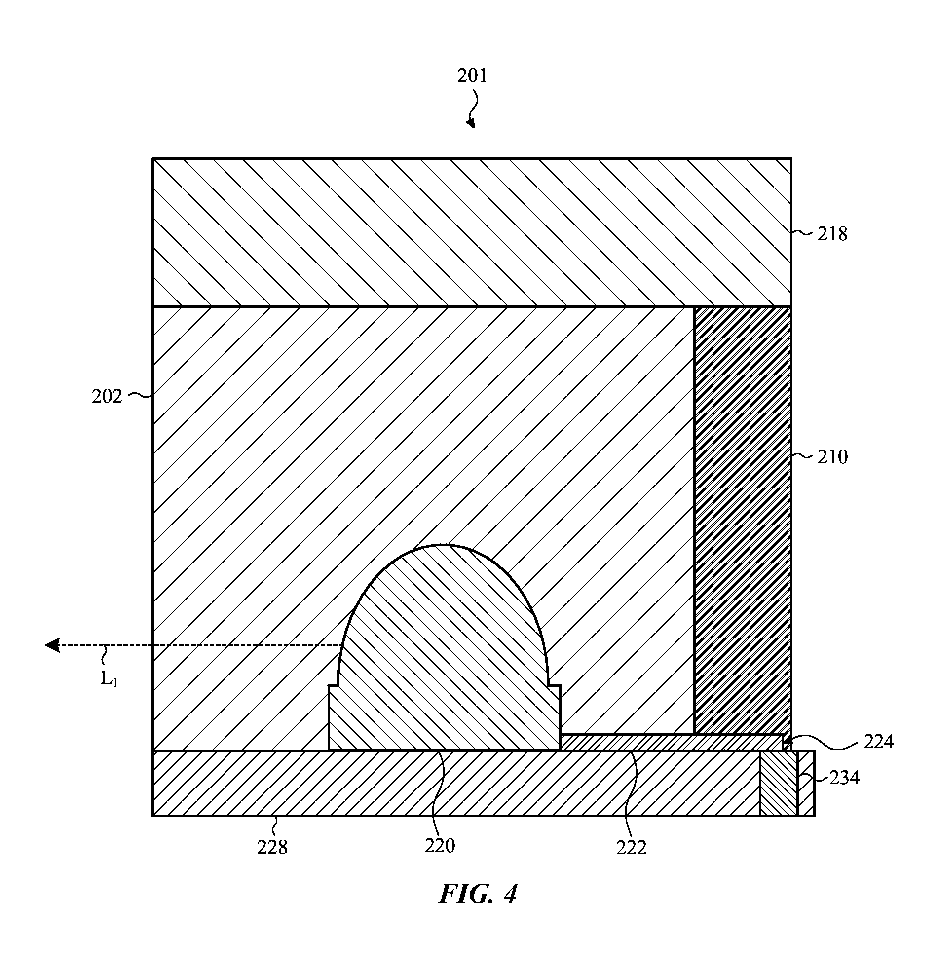
FIG. 4 shows a cross-sectional side view of the LED assembly taken along line 4-4 in FIG. 2, according to embodiments.
FIG. 5 shows an exploded view of a single key of the low-travel keyboard assembly of FIG. 2, according to embodiments.
FIG. 6 shows a cross-section view of a low-travel keyboard assembly including a switch housing taken along line CS-CS in FIG. 5, according to embodiments.
FIG. 7 shows a top view of a switch housing of a low-travel keyboard assembly including light-emitting assembly of FIGS. 2-4, according to embodiments.
FIG. 8 is a flowchart illustrating a sample method of illuminating an input surface.
DETAILED DESCRIPTION
Reference will now be made in detail to representative embodiments illustrated in the accompanying drawings. It should be understood that the following descriptions are not intended to limit the embodiments to one preferred embodiment. To the contrary, it is intended to cover alternatives, modifications, and equivalents as can be included within the spirit and scope of the described embodiments as defined by the appended claims.
The following disclosure relates generally to a keyboard assembly for an electronic device and, more particularly, to a light-emitting structure positioned within a switch housing of a keyboard assembly for an electronic device. The light-emitting structure may be a light-emitting assembly formed from a number of different elements.
In a particular embodiment, the light-emitting assembly may be formed from a light source positioned within a phosphor structure adjacent, touching, or at least partially surrounded by various layers or materials, including: sidewalls (which may be formed from a transparent material or opaque material); epoxy (which may form a sidewall and may be either opaque or transparent); a mask layer; and/or a heat dissipation layer. The light-emitting assembly generates and/or transmits light in certain directions, such as through one or more of the phosphor structure and layers. The various layers may restrict light to traveling through only three sides of the assembly, in certain embodiments.
Light exiting the light-emitting assembly generally has a common wavelength and thus common color. Where the wavelengths and colors of light traveling through all light-transmissible sides of the assembly are equal, that light may illuminate an input surface such as a keycap. Accordingly, the keycap is substantially uniformly illuminated and has reduced or no dim spots and/or color shifts. Additionally, because of the configuration of the various layers and materials forming the light-emitting assembly, the light-emitting assembly may be a parallelepiped and compact, thereby reducing the space occupied within the keyboard assembly. Finally, where each key of the keyboard assembly includes an individual light-emitting assembly, keys and/or keycaps may be illuminated individually or selectively.
These and other embodiments are discussed below with reference to FIGS. 1-7. However, those skilled in the art will readily appreciate that the detailed description given herein with respect to these Figures is for explanatory purposes only and should not be construed as limiting.
FIG. 1 shows an electronic device 100 including a low-travel keyboard assembly 200 that may incorporate a light-emitting assembly for illuminating keyboard assembly 200, as described in more detail below with respect to FIGS. 2-4. In a non-limiting example, as shown in FIG. 1, electronic device 100 may be a laptop computer. However, it is understood that electronic device 100 may be configured as any suitable electronic device that may utilize low-travel keyboard assembly 200. Other embodiments can implement electronic device 100 differently, such as, for example, a desktop computer, a tablet computing device, a telephone, a gaming device, a display, a digital music player, a wearable computing device or display, a health monitoring device, and so on.
Electronic device 100 may include a top case 102. Top case 102 may take the form of an exterior, protective casing or shell for electronic device 100 and the various internal components (for example, low-travel keyboard assembly 200) of electronic device 100. Top case 102 may be formed as a single, integral component, or may have a group of distinct components that may be configured to be coupled to one another, as discussed herein. Additionally, top case 102 may be formed from any suitable material(s) that provides a protective casing or shell for electronic device 100 and the various components included in electronic device 100. In non-limiting examples, top case 102 may be made from metal, a ceramic, a rigid plastic or another polymer, a fiber-matrix composite, and so on.
Low-travel keyboard assembly 200 may be included within electronic device 100 to allow a user to interact with electronic device 100. As shown in FIG. 1, low-travel keyboard assembly 200 is positioned within and/or may be received by top case 102 of electronic device 100. Low-travel keyboard assembly 200 may include a set of keycaps 300 positioned within and partially protruding through and/or surrounded by top case 102 of electronic device 100. As discussed herein, keycaps 300 are depressed and displaced to at least partially collapse a dome switch of low-travel keyboard assembly 200, which in turn forms an electrical signal or input to electronic device 100.
As discussed herein, keycap 300 of low-travel keyboard assembly 200 can be illuminated by a light-emitting assembly. The light-emitting assembly of low-travel keyboard assembly 200 is positioned in a switch housing surrounding a dome switch, where the switch housing and dome switch are positioned below keycap 300. That is, each individual keycap 300 includes an individual switch housing, which includes an individual light-emitting assembly positioned therein. As a result, a single light-emitting assembly illuminates each corresponding keycap 300. This can improve brightness and light uniformity for each keycap, and between keycaps.
Additionally, because each keycap 300 is illuminated by a single, corresponding light-emitting assembly, keycaps 300 of keyboard assembly 200 can be illuminated individually or selectively. In some embodiments, other illumination schemes may be used. For example, adjacent of keys can be lit by a single light-emitting assembly (e.g., one light-emitting assembly for each group of keys). In other embodiments, a row or column of keys may be illuminated by a single light-emitting assembly. In still other embodiments, light source assemblies may be located at different points under a keyboard so that a relatively small number of assemblies may illuminate an entire keyboard (or all keycaps of the keyboard). In any or all embodiments, light source assemblies may be located within or outside of switch housings, under keycaps, or under portions of the casing. Further, light source assemblies described herein may be used with other input devices, including mice, track pads, buttons, switches, touch-sensitive and/or force-sensitive surfaces, and so on.
The light source assemblies of low-travel keyboard assembly 200 are formed from a light source positioned within a phosphor structure surrounded by various layers or materials that may include one or more transparent materials, one or more epoxy layers and one or more mask layers. The various layers to allow light to be emitted from only three sides of the assembly. Further, the emitted light has identical wavelengths and color. Where the wavelengths and visible light color are identical on all sides of the assembly, keycap 300 of low-travel keyboard assembly 200 is illuminated by the light-emitting assembly with a consistent visible light color and does not have discrepancies in illuminating light color or intensity.
Additionally, and as discussed herein, because of the configuration of the various layers and materials forming the light-emitting assembly, the light-emitting assembly can be a parallelepiped. The parallelepiped shape of the light-emitting assembly of low-travel keyboard assembly may reduce the overall size of light-emitting assembly and/or makes light-emitting assembly substantially compact. With a reduced size, the required amount of space occupied by light-emitting assembly within keyboard assembly 200 may also be reduced. This ultimately allows for low-travel keyboard assembly 200 and/or electronic device 100 to have a reduced size as well. It should be appreciated that substantially any other geometric or non-geometric three-dimensional shape may also be used for a light-emitting assembly.
In the non-limiting example shown in FIG. 1, where electronic device 100 is a laptop computer, low-travel keyboard assembly 200 may be positioned within and/or may be received by electronic device 100. In an additional embodiment, low-travel keyboard assembly 200 may be a distinct, standalone component and may be in electronic communication, whether wired or wireless, with electronic device 100. Low-travel keyboard assembly 200 may be configured to allow a user to interact with electronic device 100.
FIG. 2 shows a light-emitting assembly 201 of low-travel keyboard assembly 200 (see, FIGS. 1 and 5-7). Light-emitting assembly 201 may emit a light that travels from the assembly, into a switch housing, and is redirected by the switch housing to illuminate keycap 300. With the spatial constraints of light source recess 404 of switch housing 400 (see, FIGS. 5-7), discussed herein, light-emitting assembly 201 may be configured to fit in light source recess 404 and provide light to keycap 300, including during operation of low-travel keyboard assembly 200.
Light-emitting assembly may have a phosphor structure 202 and transparent material 204 positioned on opposing sides surfaces of phosphor structure 202. In some embodiments, the transparent material may be positioned on or otherwise abutting the phosphor material, either wholly or partially. The phosphor structure may be a phosphor-doped material and may overlay a light source 220. In some embodiments, the phosphor structure may alter a wavelength of a light emitted by the light source, thereby altering its color. Further, in some embodiments the phosphor structure may luminesce (e.g., emit light) when the light source is active. Thus, the phosphor structure may be a luminescent structure. As discussed herein, phosphor structure 202 and transparent material 204 may allow light from a light source of light-emitting assembly 201 to be emitted through the respective portions.
The transparent material 204 may permit light to travel therethrough. Any suitable material may be used as the transparent material, including various plastics, polymers, ceramics, glasses, and so on.
Light source 220 of light-emitting assembly 201 may be positioned within phosphor structure 202. As shown in the cross-sectional views of FIGS. 3 and 4, light source 220 may be positioned substantially in the center of, and substantially encompassed within, phosphor structure 202 of light-emitting assembly 201. Light source 220 may emit a light through phosphor structure 202 and transparent material 204 and, ultimately, through switch housing 400 of low-travel keyboard assembly 200, as discussed herein with respect to FIGS. 5-7. In some embodiments, the light source 220 may be off-center with respect to the phosphor structure 202 and/or light-emitting assembly 201.
A variety of different light sources 220 may be used in the light-emitting assembly 201. For example, the light source 220 may be a light-emitting diode, an organic light-emitting diode, a quantum dot, a cold cathode fluorescent lamp, and so on. Further, the light source may emit multiple colors of light in some embodiments. As an example, the light source may be a multicolor LED and the color emitted by the LED may change based on a user input, operating state, software or firmware command, and so on. Some embodiments may also employ multiple light sources 220 in a single light-emitting assembly 201.
Light-emitting assembly 201 may also have an epoxy layer 210 placed over an entire back surface 212 of phosphor structure 202 and transparent material 204. In one embodiment, epoxy layer 210 may be substantially larger in one or more dimension than phosphor structure 202 and transparent material 204, although this may vary between embodiments. More specifically, as shown in FIG. 2, epoxy layer 210 may be substantially wider than phosphor structure 202 and transparent material 204 an example of this is shown in FIG. 4.
Returning to FIG. 2, epoxy layer 210 may be adjacent or abutting back surface 212 of phosphor structure 202 and transparent material 204, which may substantially waterproof light-emitting assembly 201 and its components. In non-limiting examples, epoxy layer 210 may be substantially transparent to allow light from light source 220 to pass through epoxy layer 210. Alternatively, epoxy layer 210 may be opaque epoxy and prevent light from passing through epoxy layer 210. In some embodiments, the transparent material 204 may be formed on the phosphor structure; likewise in some embodiments the epoxy may be directly formed on the back surface (e.g., rear). In other embodiments, the transparent material and/or epoxy layer may be deposited or layered, rather than formed, on their corresponding surfaces.
Light-emitting assembly 201 may also incorporate a mask layer 218. Mask layer 218 may be positioned over phosphor structure 202, transparent material 204 and/or epoxy layer 210 of light-emitting assembly 201. In a non-limiting example shown in FIG. 2, phosphor structure 202, transparent material 204 and epoxy layer 210 of light-emitting assembly 201 may have top surfaces that may be in planar alignment and may be substantially covered by mask layer 218. Mask layer 218 may be formed from an opaque material to prevent light of light source 220 from being emitted through mask layer 218.
With continued reference to FIG. 2, FIGS. 3 and 4 show cross-section views of LED assembly 201. Specifically, FIG. 3 shows a cross-sectional front view of LED assembly 201 taken along line 3-3 in FIG. 2, and FIG. 4 shows a cross-sectional side view of LED assembly 201 taken along line 4-4 in FIG. 2. As shown in FIG. 4, light source 220 may have one or more electrical leads 222 electrically coupled to light source 220 and a substrate 228, such as a printed circuit board (PCB) 500 of low travel keyboard assembly 200 (see, FIGS. 5-7), to provide power to light source 220. In the non-limiting example shown in FIGS. 2-4, the electrical leads 222 electrically couple light source 220 to substrate 228, such that substrate 228 may provide power to light source 220, as discussed herein. As shown in FIGS. 2 and 4, the electrical leads 222 may be positioned in phosphor structure 202 and may extend toward back surface 212 of phosphor structure 202. Portions of the leads 222 of light source 220 may also extend through or be positioned within epoxy layer 210, so that epoxy layer 210 seals (e.g., waterproofs) the electrical leads 222 and, ultimately, light source 220, to prevent light source 220 from undesirably shorting due to moisture exposure. As shown in FIG. 4, the portion of the electrical leads 222 placed and sealed within epoxy layer 210 may be an end portion 224 of leads 222, which may be electrically coupled to and/or in electronic communication with a light source contact 234 of substrate 228 for receiving power for light source 220.
Light-emitting assembly 201 may also have a heat dissipation layer 226 over mask layer 218. Heat dissipation layer 226 may be formed from a heat resistant material that may dissipate the heat generated by light source 220 and the light generated by light source 220. As light is emitted from light source 220, light may contact mask layer 218, but may not be emitted through opaque mask layer 218. However, the light and light source 220 may generate heat on or in mask layer 218. Heat dissipation layer 226 may be positioned on mask layer 218 to dissipate the heat exposed to mask layer 218, which in turn reduce or prevent chemical and/or physical changes to mask layer 218. In some embodiments, the mask layer and heat dissipation layer may be the same layer, or formed from the same material. For example, a thermally conductive mask layer may be used.
In some embodiments, the transparent material(s) 204, mask layer 218, heat dissipation layer 226, and/or epoxy layer 210 may be affixed to the phosphor structure 202. This may be accomplished by any or all of an additional element such as an adhesive or fastener, an inherent property of one or more parts of the light-emitting assembly 201, or the method of manufacture for the assembly. It should be appreciated that the various parts of the light-transmitting assembly 201 need not be affixed to one another. For example, they may be affixed to substrate 228 such as a printed circuit board 500 or to a switch housing 400 (see, FIGS. 5 and 6) instead.
FIGS. 2-4 show light rays, labeled L.sub.1-3, emanating from light source 220. These rays are examples and are not intended to illustrate any limiting angle for emitted light. Rather, the light source 220 may emit light at any angle and direction, including out-of-plane with the illustrated light rays. Thus, for example, the light source may emit light in a hemispherical pattern, near-spherical pattern, conic pattern, and so on. Accordingly, the light rays are intended to show overall, sample directions of emitted light and particularly how light may pass through certain surfaces of the light-emitting assembly 201.
In one embodiment, light may be emitted through three sides of light-emitting assembly 201. In the non-limiting example shown in FIGS. 4-6, light (L.sub.1) may be emitted through a front face of light-emitting assembly 201 including phosphor structure 202. Likewise light (L.sub.2) may be emitted through a first sidewall 230 defined by transparent material 204. Additionally, light (L.sub.3) may be emitted through a second sidewall 232 of light-emitting assembly 201 including transparent material 204. The second side surface 232 may be opposite first side surface 230. The first and second side surfaces may be sidewalls.
Light (L.sub.1) emitted through the front face of light-emitting assembly 201 may have a wavelength substantially equal to a wavelength of light (L.sub.2) emitted through first transparent sidewall 230 and a wavelength of light (L.sub.3) emitted through second transparent sidewall 232. As a result of the wavelengths of light (L.sub.1-3) being equal, the visible light color of the light (L.sub.1-3) may also be identical or substantially the same. That is, the visible light color of the light (L.sub.1) emitted through the front face of light-emitting assembly 201 may be substantially identical to a visible light color of light (L.sub.2) emitted through first transparent sidewall 230 and a visible light color of light (L.sub.3) emitted through second transparent sidewall 232.
As shown in FIGS. 2-4, light-emitting assembly 201 may be a parallelepiped, or substantially a parallelepiped. Further, phosphor structure 202 and transparent material 204 positioned on opposite sides of surfaces of phosphor structure 202 may be substantially parallelepiped-shaped. Other embodiments may employ light-emitting assemblies 201 of any suitable shape and/or size, including irregular shapes. Likewise, a shape of the phosphor structure 202 need not match a shape of the overall assembly.
As a result of its geometry, light-emitting assembly 201 may require less space in low-travel keyboard assembly 200, as discussed herein with respect to FIGS. 5-7. Further, the aforementioned transparent material may form one or more transparent sidewalls of the light-emitting assembly. For example and as shown in FIG. 2, opposing sidewalls may be formed from the transparent material. Similarly, a rear or back surface of the light-emitting assembly may be formed from epoxy or another suitable material, and may be opaque. A front face of the light-emitting assembly 201 may be formed by a front surface of the phosphor structure. A mask layer may overlay the phosphor structure and upper surfaces of the sidewalls, thereby defining a top of the assembly. As also shown in FIG. 2, the phosphor structure may abut the sidewalls and the opaque material forming the rear, although other embodiments may include spaces between any or all of the foregoing. Further and as shown in FIGS. 2-4, the phosphor structure may fill an interior of the light-emitting assembly, as defined by the sidewalls, rear, and mask layer.
Additionally, because of the geometric shape of light-emitting assembly 201 and the inclusion of transparent material 204 positioned on opposite sides of phosphor structure 202, the wavelength and, ultimately, the visible light color of the light emitted by light source 220 may be substantially identical on all sides of light-emitting assembly 201. That is, the greater the thickness of phosphor structure 202 in which light from light source 220 must travel through, the more the wavelength of the light will change. However, a wavelength of light from light-emitting assembly 201 may be tuned by adding or removing more transparent material 204. This may ensure that the wavelength of light (L.sub.1) emitted through the front face, including front surface of phosphor structure 202, is equal to the wavelengths of the light (L.sub.2, L.sub.3) emitted through first sidewall and second sidewall including transparent material 204. And, as discussed herein, wherein the wavelengths of light emitted through light-emitting assembly 201 are equal, the visible light color of light emitted through light-emitting assembly 201 may also be identical or substantially the same, creating a uniform illumination color for keycap 300 of keyboard assembly 200 (see, FIGS. 5-7).
FIGS. 5 and 6 show a sample key structure of low-travel keyboard assembly 200 that utilizes light-emitting assembly 201 (see, FIG. 6), according to non-limiting examples. Specifically, FIG. 5 shows a detailed exploded view of a portion of top case 102 of electronic device 100 and a single key structure 502 that utilizes light-emitting assembly 201, as discussed herein. FIG. 6 shows a cross-section view of the single key assembly 502, taken along line CS-CS of FIG. 5. It is understood that similarly named components or similarly numbered components may function in a substantially similar fashion, may include similar materials and/or may include similar interactions with other components. Redundant explanation of these components has been omitted for clarity.
As shown in FIG. 5, top case 102 of electronic device 100 (see, FIG. 1) may include one or more keyholes 104 formed therethrough. Top case 102 may also include ribs or other supports 106 between or about the keycaps 300, and may substantially surround and/or may be positioned within the space between the keycaps 300 of low-travel keyboard assembly 200.
Low-travel keyboard assembly 200 may be made from a number of layers or components positioned adjacent to and/or coupled to one another. The components positioned in layers may be positioned adjacent to and/or coupled to one another, and may be sandwiched between top case 102 and a bottom case (not shown) of electronic device 100.
The keycaps 300 of low-travel keyboard assembly 200 may be positioned at least partially within keyholes 104 of top case 102. Each of the keycaps 300 may include a glyph 302 positioned on a top or exposed surface of the keycap 300. Each glyph 302 of keycap 300 may be substantially transparent to allow a light to be emitted through and/or illuminate keycap 300. In the non-limiting example shown in FIGS. 5 and 6, keycap 300 may be substantially opaque, except for glyph 302, which may be transparent to allow light to be emitted through keycap 300. Additionally, the perimeter of keycap 300 may be substantially illuminated by light emitted between the space between keycap 300 and skeletal ribs 106 of top case 102.
As shown in FIG. 6, keycap 300 of low-travel keyboard assembly 200 may include retaining members 304, 306 positioned on keycap 300. More specifically, keycap 300 may include at least one first retaining member 304 positioned on first side 308 and at least one second retaining member 306 positioned on a second side 310 of keycap 300, opposite first side 308. Retaining members 304, 306 may be formed, positioned, or retained on an underside 312 of keycap 300 adjacent a switch housing 400 of low-travel keyboard assembly 200. The retaining members 304, 306 may be utilized to couple keycap 300 within low-travel keyboard assembly 200 and, specifically, to couple keycap 300 to a hinge mechanism 322 coupled to PCB 500. Hinge mechanism 322, as shown in FIG. 6, may include any suitable hinge mechanism 322 capable of moving keycap 300 from an undepressed (e.g., rest) state to a depressed state, including, but not limited to, a butterfly hinge mechanism, a scissor hinge mechanism, a telescoping hinge mechanism or a sliding hinge mechanism. Hinge mechanism 322 may be coupled to and/or positioned within recess a 502 formed in PCB 500 of low-travel keyboard assembly 200.
The keycaps 300 may be positioned above corresponding switch housings 400 of low-travel keyboard assembly 200, and may interact with a corresponding switch housing 400. Each switch housing 400 of low-travel keyboard assembly 200 may include a switch opening 402 extending completely through switch housing 400, and a light source recess 404 formed within each switch housing 400. Some switch housings 400 may define multiple light source recesses 404, each of which may house its own light-emitting assembly 201 or multiple assemblies. Further, the light source recess 404 may be sized such that one or more of its interior walls engage the exterior of the light-emitting assembly 201, or gaps may exist between the interior walls of the light source recess and any or all parts of the light-emitting assembly's exterior.
As shown in FIG. 6, switch opening 402 may receive and/or house dome switch 406, which may be collapsed in response to keycap 300 translating. The dome switch collapses (or partially collapse) to generate an electrical connection acting as a signal to electronic device 100 (see, FIG. 1). Additionally, as shown in FIG. 6, light source recess 404 of switch housing 400 may receive light-emitting assembly 201, which may emit a light through switch housing 400 to provide a light around the perimeter of keycap 300 and/or through transparent glyph 302 (see, FIG. 5) of keycap 300. Additionally in another non-limiting example, light-emitting assembly 201 may emit light directly toward recess 502 to aid in illuminating the perimeter of keycap 300. Although discussed herein as a dome switch, it is understood that switch opening 402 may receive or house different types of switches.
As also shown in FIG. 6, switch housing 400 may include a body portion 410 and a top panel 412 formed integrally and molded to body portion 410. Body portion 410 of switch housing 400 may include switch opening 402 and light source recess 404 adjacent switch opening 402. Body portion 410 may be directly coupled to PCB 500, as shown in FIG. 6.
Body portion 410 and top panel 412 of switch housing 400 may be formed from distinct materials. That is, body portion 410 may be formed from a first material having substantially rigid properties for supporting keycap 300 during operation of low-travel keyboard assembly 200 and/or protecting the various components (e.g., dome switch 406, light-emitting assembly 201) included within switch housing 400. The first material forming body portion 410 of switch housing 400 may also be transparent and/or reflective to direct light out of the switch housing and toward the keycap 300. In a non-limiting example, light source 220 of light-emitting assembly 201 may emit light through transparent switch housing 400, and switch housing 400 may substantially reflect and/or allow light to be transmitted through the transparent material of switch housing 400 to illuminate glyph 302 on keycap 300 and/or the perimeter of keycap 300.
The top panel 412 may act as a light guide to direct light emitted from light-emitting assembly 201 to keycap 300. The top panel 412 may include structures configured to focus light on specific areas of the keycap or about the keycap, as well as reflective structures configured to direct light toward the keycap. For example, lenses, apertures, and the like may emit light from the top panel, while an upper surface of the top panel may reflect light incident on the panel.
Top panel 412 of switch housing 400 may be formed integrally with body portion 410. As one example, as shown in FIG. 6, top panel 412 may be overmolded on body portion 410 and may cover switch opening 402 of body portion 410. In a non-limiting example, top panel 412 may be formed integrally with body portion 410 using a double-shot housing formation process. Top panel 412 may be formed from a second material, distinct from the first material forming body portion 410, and may be substantially flexible/deformable. As discussed herein, top panel 412 may substantially flex and protect dome switch 406 when keycap 300 is depressed. In addition to being flexible, the second material forming top panel 412 may have substantially transparent properties that allow light to pass through top panel 412 to keycap 300 and/or substantially reflective properties to redirect light toward keycap 300.
Top panel 412 may be positioned over switch opening 402 not only to redirect light toward keycap 300 but also to substantially protect dome switch 406 from wear. That is, when a force is applied to keycap 300 to depress keycap 300, keycap 300 may contact top panel 412 of switch housing 400, which may subsequently deform and collapse dome switch 406 to form an electrical connection. By acting as a barrier between keycap 300 and dome switch 406, top panel 412 may reduce the wear on dome switch 406 over the operational life of low-travel keyboard assembly 200.
Top panel 412 may also include a first contact protrusion 418 positioned on a first surface 420 of the top panel 412. First contact protrusion 418 may be positioned directly adjacent a second contact protrusion 340 on underside 312 of keycap 300. The first contact protrusion 418 of top panel 412 and the second contact protrusion 340 of keycap 300 may contact one another when keycap 300 is depressed and may more evenly distribute the force applied to top panel 412 and, subsequently, dome switch 406 when keycap 300 is depressed. By distributing the force through top panel 412, the wear on dome switch 406 may be further reduced over the operational life of low-travel keyboard assembly 200.
Switch housing 400 may also include a roof portion 426 over light source recess 404. More specifically, body portion 410 of switch housing 400 may include a roof portion 426 positioned over light source recess 404 and light-emitting assembly positioned within light source recess 404. As shown in FIG. 6, roof portion 426 of switch housing 400 may be formed integrally with switch housing 400 and, specifically, body portion 410 of switch housing 400. However, it is understood that roof portion 426 of switch housing 400 may be formed from a distinct component or material that may be coupled to body portion 410 of switch housing 400. Roof portion 426 of switch housing 400 may be substantially opaque to prevent the light of light-emitting assembly 201 from being emitted through roof portion 426. In a non-limiting example, substantially opaque roof portion 426 may work in conjunction with mask layer 218 of light-emitting assembly 201, as discussed herein with respect to FIG. 4, to prevent light from passing directly toward keycap 300 and/or through roof portion 426 of switch housing 400.
Low-travel keyboard assembly 200 may also include a printed circuit board (PCB) 500 positioned below the group of switch housings 400. PCB 500 may be similar to substrate 228 discussed herein with respect to FIGS. 2-4. As shown in FIGS. 5 and 6, switch housings 400 may be coupled to PCB 500 of low-travel keyboard assembly 200. More specifically, PCB 500 may include a number of recesses 502 within PCB 500, where each recess 502 of PCB 500 may receive a corresponding switch housing 400 of low-travel keyboard assembly 200. Each switch housing 400 may be positioned completely within, and coupled to the surface of, recess 502 of PCB 500. PCB 500 may provide a rigid support structure for switch housing 400, and the various components forming low-travel keyboard assembly 200.
PCB 500 may also include one or more apertures 504 extending through each of the recesses 502. That is, aperture 504 may pass completely through PCB 500 in recess 502. As shown in FIGS. 5 and 6, aperture 504 of PCB 500 may be substantially aligned with switch opening 402 of switch housing 400 of low-travel keyboard assembly 200. The apertures 504 of PCB 500 may be utilized to receive a portion of the dome switch positioned within switch housing 400 when the dome switch collapses.
As shown in FIG. 6 and discussed herein with respect to FIGS. 2-4, light-emitting assembly 201 and, specifically, leads 222 of light source 220 may be in electrical contact with light source contact 234 extending from or through PCB 500. Light source contact 234 may be in communication with a light source driver 530 positioned on second surface 518 of PCB 500. PCB 500 may have a number of light source drivers 530 positioned on second surface 518, where each light source driver 530 corresponds to, and is in electronic communication with, light-emitting assembly 201 of low-travel keyboard assembly 200. light source drivers 530 positioned on second surface 518 of PCB 500 may be configured to provide power and/or control to light-emitting assembly 201 during operation of low-travel keyboard assembly 200 included in electronic device 100 (see, FIG. 1). It is understood that FIG. 6, showing a single key assembly, may represent some or all of the keys for low-travel keyboard assembly 200. Where each key assembly of low-travel keyboard assembly 200 is structured similar to the key assembly shown in FIG. 6, each switch housing 400 for each key of low-travel keyboard assembly 200 may have light-emitting assembly 201. As a result, each individual keycap 300 may be illuminated by the corresponding individual light-emitting assembly 201.
Low-travel keyboard assembly 200, as shown in FIGS. 5 and 6, may include a keyboard shield 600 positioned below PCB 500. Keyboard shield 600 may be formed from a conductive adhesive sheet 602 adhered to PCB 500 opposite switch housing 400. Conductive adhesive sheet 602 of shield 600 may include a venting system 604, which vents air expelled from switch housing 400 when dome switch 406 collapses, as discussed herein. As shown in FIGS. 5 and 6, venting system 604 may include a group of channels 606 formed within and/or partially through conductive adhesive sheet 602 of shield 600 which may be in fluid communication and/or may be substantially aligned with dome switch opening 402 formed in switch housing 400 and aperture 504 formed through PCB 500. Conductive adhesive sheet 602 of keyboard shield 600 may be utilized to transmit signals to and/or from keyboard assembly 200 of electronic device 100 during user interaction.
FIG. 7 shows a top view of switch housing 400 including light-emitting assembly 201. Roof portion 426 of switch housing 400 and mask layer 218 of light-emitting assembly 201 are omitted in FIG. 7 to clearly show light-emitting assembly 201 positioned within light source recess 404 of switch housing 400. As discussed herein with respect to FIGS. 2 and 6, roof portion 426 of switch housing 400 and mask layer 218 of light-emitting assembly 201 may prevent light from passing through roof portion 426, directly toward keycap 300. As shown in FIG. 7, light-emitting assembly 201 may be substantially surrounded by three sidewalls 450 of light source recess 404 of switch housing 400. In one example, light source recess 404 may be bounded by three sidewalls 450 to ensure that light emitted by light-emitting assembly 201 passes through a large portion of switch housing 400 and subsequently illuminates keycap 300 of low-travel keyboard assembly 200. That is, by substantially surrounding light-emitting assembly 201 with sidewalls 450 of light source recess 404, a majority of light (L.sub.1-3) may directly pass through switch housing 400 and/or switch housing 400 may reflect light (L.sub.1-3) toward keycap 300.
As shown in FIG. 7, light-emitting assembly 201 may be surrounded by a curable, transparent resin 236 (hereafter, "resin 236") that may be positioned between light-emitting assembly 201 and sidewalls 450 of light source recess 404 of switch housing 400. Resin 236 may be formed or placed over light-emitting assembly 201 after light-emitting assembly 201 is positioned within light source recess 404 of switch housing 400, to retain light-emitting assembly in light source recess 404 and/or to seal light-emitting assembly 201 from outside contaminants (e.g., water). Additionally, resin 236 may aid in dissipating heat from light-emitting assembly during operation of low-travel keyboard assembly 200. Furthermore, the transparent characteristics or properties of resin 236 may allow light to pass through resin 236 toward recess 502 to aid in illuminating the perimeter of keycap 300, as discussed herein.
Operation of a sample embodiment will now be described with respect to FIG. 8. Initially, in operation 800 a light source may be activated. Light may be transmitted from the light source and through the light-emitting assembly in operation 802. For example, light may pass through the phosphor structure and/or transparent material of the light-emitting assembly. Likewise, light may be blocked from exiting the assembly in certain directions, for example by the mask layer and/or epoxy. The phosphor material may color-shift the light as it passes therethrough, although this is not necessary.
In operation 804, light may exit the light-emitting assembly and enter an associated switch housing. A body of the switch housing may redirect the light upward, for example toward a top panel of the switch housing. In some embodiments, the body (or portions thereof) may be reflective to facilitate redirection of light. In other embodiments, light may not be substantially redirected or may be moderately or minimally redirected. Further, the top panel may act as a light guide to redirect light from the switch housing toward a key cap or other input surface
In operation 806, light may exit the top panel and emanate toward an underside of the key cap or other input surface. In operation 808, the light may illuminate a glyph on the key cap and/or may illuminate a perimeter of the key cap.
Although discussed herein as a keyboard assembly, it is understood that the disclosed embodiments may be used in a variety of input devices used in various electronic devices. That is, low-travel keyboard assembly 200 and the components of the assembly discussed herein may be utilized or implemented in a variety of input devices for an electronic device including, but not limited to, buttons, switches, toggles, wheels, and touch screens.
The foregoing description, for purposes of explanation, used specific nomenclature to provide a thorough understanding of the described embodiments. However, it will be apparent to one skilled in the art that the specific details are not required in order to practice the described embodiments. Thus, the foregoing descriptions of the specific embodiments described herein are presented for purposes of illustration and description. They are not targeted to be exhaustive or to limit the embodiments to the precise forms disclosed. It will be apparent to one of ordinary skill in the art that many modifications and variations are possible in view of the above teachings.
* * * * *
References
D00000
D00001
D00002
D00003
D00004
D00005
D00006
D00007
D00008
XML
uspto.report is an independent third-party trademark research tool that is not affiliated, endorsed, or sponsored by the United States Patent and Trademark Office (USPTO) or any other governmental organization. The information provided by uspto.report is based on publicly available data at the time of writing and is intended for informational purposes only.
While we strive to provide accurate and up-to-date information, we do not guarantee the accuracy, completeness, reliability, or suitability of the information displayed on this site. The use of this site is at your own risk. Any reliance you place on such information is therefore strictly at your own risk.
All official trademark data, including owner information, should be verified by visiting the official USPTO website at www.uspto.gov. This site is not intended to replace professional legal advice and should not be used as a substitute for consulting with a legal professional who is knowledgeable about trademark law.