Detecting an active pen using a capacitive sensing device
Shepelev , et al. J
U.S. patent number 10,175,827 [Application Number 14/581,683] was granted by the patent office on 2019-01-08 for detecting an active pen using a capacitive sensing device. This patent grant is currently assigned to SYNAPTICS INCORPORATED. The grantee listed for this patent is Synaptics Incorporated. Invention is credited to Adam Schwartz, Petr Shepelev.


| United States Patent | 10,175,827 |
| Shepelev , et al. | January 8, 2019 |
Detecting an active pen using a capacitive sensing device
Abstract
In an example, a processing system for an integrated display and capacitive sensing device includes a sensor module and a determination module. The sensor module includes sensor circuitry configured to be coupled to a plurality of sensor electrodes. The sensor module is configured to receive an active pen signal with at least one sensor electrode of the plurality the sensor electrodes. The determination module is configured to adjust a sensing period of the sensor module for alignment with a transmission period of the active pen signal.
| Inventors: | Shepelev; Petr (San Jose, CA), Schwartz; Adam (Redwood City, CA) | ||||||||||
|---|---|---|---|---|---|---|---|---|---|---|---|
| Applicant: |
|
||||||||||
| Assignee: | SYNAPTICS INCORPORATED (San
Jose, CA) |
||||||||||
| Family ID: | 56129332 | ||||||||||
| Appl. No.: | 14/581,683 | ||||||||||
| Filed: | December 23, 2014 |
Prior Publication Data
| Document Identifier | Publication Date | |
|---|---|---|
| US 20160179226 A1 | Jun 23, 2016 | |
| Current U.S. Class: | 1/1 |
| Current CPC Class: | G06F 3/0442 (20190501); G09G 3/20 (20130101); G06F 3/044 (20130101); G06F 3/03545 (20130101); G06F 2203/04108 (20130101); G06F 3/0443 (20190501); G06F 3/0445 (20190501) |
| Current International Class: | G06F 3/0354 (20130101); G06F 3/044 (20060101) |
References Cited [Referenced By]
U.S. Patent Documents
| 4087625 | May 1978 | Dym et al. |
| 4233522 | November 1980 | Grummer et al. |
| 4237421 | December 1980 | Waldron |
| 4264903 | April 1981 | Bigelow |
| 4293987 | October 1981 | Gottbreht et al. |
| 4484026 | November 1984 | Thornburg |
| 4492958 | January 1985 | Minami |
| 4550221 | October 1985 | Mabusth |
| 4550310 | October 1985 | Yamaguchi et al. |
| 4659874 | April 1987 | Landmeier |
| 4667259 | May 1987 | Uchida et al. |
| 4677259 | June 1987 | Abe |
| 4705919 | November 1987 | Dhawan |
| 4771138 | September 1988 | Dhawan |
| 4878013 | October 1989 | Andermo |
| 4954823 | September 1990 | Binstead |
| 4999462 | March 1991 | Purcell |
| 5053715 | October 1991 | Andermo |
| 5062916 | November 1991 | Aufderheide et al. |
| 5093655 | March 1992 | Tanioka et al. |
| 5239307 | August 1993 | Andermo |
| 5341233 | August 1994 | Tomoike et al. |
| 5392058 | February 1995 | Tagawa |
| 5459463 | October 1995 | Gruaz et al. |
| 5463388 | October 1995 | Boie et al. |
| 5534892 | July 1996 | Tagawa |
| 5650597 | July 1997 | Redmayne |
| 5657012 | August 1997 | Tait |
| 5777596 | July 1998 | Herbert |
| 5841078 | November 1998 | Miller et al. |
| 5869790 | February 1999 | Shigetaka et al. |
| 5896120 | April 1999 | Iguchi et al. |
| 6054979 | April 2000 | Sellers |
| 6188391 | February 2001 | Seely et al. |
| 6219113 | April 2001 | Takahara |
| 6222522 | April 2001 | Mathews et al. |
| 6239788 | May 2001 | Nohno et al. |
| 6256022 | July 2001 | Manaresi et al. |
| 6281888 | August 2001 | Hoffman et al. |
| 6288707 | September 2001 | Philipp |
| 6297811 | October 2001 | Kent et al. |
| 6307751 | October 2001 | Bodony et al. |
| 6320394 | November 2001 | Tartagni |
| 6362633 | March 2002 | Tartagni |
| 6380930 | April 2002 | Van Ruymbeke |
| 6452514 | September 2002 | Philipp |
| 6459044 | October 2002 | Watanabe et al. |
| 6486862 | November 2002 | Jacobsen et al. |
| 6512381 | January 2003 | Kramer |
| 6535200 | March 2003 | Philipp |
| 6560276 | May 2003 | Long et al. |
| 6583632 | June 2003 | Von Basse et al. |
| 6653736 | November 2003 | Kishimoto et al. |
| 6731120 | May 2004 | Tartagni |
| 6771327 | August 2004 | Sekiguchi |
| 6825833 | November 2004 | Mulligan et al. |
| 6879930 | April 2005 | Sinclair et al. |
| 6910634 | June 2005 | Inose et al. |
| 6937031 | August 2005 | Yoshioka et al. |
| 6998855 | February 2006 | Tartagni |
| 7031886 | April 2006 | Hargreaves |
| 7129935 | October 2006 | Mackey |
| 7158125 | January 2007 | Sinclair et al. |
| 7218314 | May 2007 | Itoh |
| 7306144 | December 2007 | Moore |
| 7327352 | February 2008 | Keefer et al. |
| 7339579 | March 2008 | Richter et al. |
| 7348967 | March 2008 | Zadesky et al. |
| 7382139 | June 2008 | Mackey |
| 7388571 | June 2008 | Lowles et al. |
| 7423219 | September 2008 | Kawaguchi et al. |
| 7423635 | September 2008 | Taylor et al. |
| 7439962 | October 2008 | Reynolds et al. |
| 7455529 | November 2008 | Fujii et al. |
| 7522230 | April 2009 | Lee |
| 7548073 | June 2009 | Mackey et al. |
| 7554531 | June 2009 | Baker et al. |
| 7589713 | September 2009 | Sato |
| 7633566 | December 2009 | Utsunomiya et al. |
| 7663607 | February 2010 | Hotelling et al. |
| 7724243 | May 2010 | Geaghan |
| 7768273 | August 2010 | Kalnitsky et al. |
| 7786981 | August 2010 | Proctor |
| 7808255 | October 2010 | Hristov et al. |
| 7812825 | October 2010 | Sinclair et al. |
| 7821274 | October 2010 | Philipp et al. |
| 7821502 | October 2010 | Hristov |
| 7859521 | December 2010 | Hotelling et al. |
| 7864160 | January 2011 | Geaghan et al. |
| 7876309 | January 2011 | XiaoPing |
| 7973771 | July 2011 | Geaghan |
| 7977953 | July 2011 | Lee |
| 7986152 | July 2011 | Philipp et al. |
| 8040326 | October 2011 | Hotelling et al. |
| 8059015 | November 2011 | Hua et al. |
| 8125463 | February 2012 | Hotelling et al. |
| 8243027 | August 2012 | Hotelling et al. |
| 8258986 | September 2012 | Makovetskyy |
| 8259078 | September 2012 | Hotelling et al. |
| 8278571 | October 2012 | Orsley |
| 8305359 | November 2012 | Bolender et al. |
| 8319747 | November 2012 | Hotelling et al. |
| 8482536 | July 2013 | Young |
| 9164641 | October 2015 | Rowe |
| 2002/0077313 | June 2002 | Clayman |
| 2003/0052867 | March 2003 | Shigetaka et al. |
| 2003/0103043 | June 2003 | Mulligan et al. |
| 2003/0234771 | December 2003 | Mulligan et al. |
| 2004/0062012 | April 2004 | Murohara |
| 2004/0077313 | April 2004 | Oba et al. |
| 2004/0095336 | May 2004 | Hong et al. |
| 2004/0125087 | July 2004 | Taylor et al. |
| 2004/0217945 | November 2004 | Miyamoto et al. |
| 2004/0222974 | November 2004 | Hong et al. |
| 2004/0239650 | December 2004 | Mackey |
| 2004/0252109 | December 2004 | Trent et al. |
| 2005/0030048 | February 2005 | Bolender et al. |
| 2005/0135492 | June 2005 | Jia et al. |
| 2006/0012575 | January 2006 | Knapp et al. |
| 2006/0038754 | February 2006 | Kim |
| 2006/0097991 | May 2006 | Hotelling et al. |
| 2006/0114240 | June 2006 | Lin |
| 2006/0114241 | June 2006 | Lin |
| 2006/0114247 | June 2006 | Brown |
| 2006/0232600 | October 2006 | Kimura et al. |
| 2007/0008299 | January 2007 | Hristov |
| 2007/0026966 | February 2007 | Sanchez |
| 2007/0074914 | April 2007 | Geaghan et al. |
| 2007/0222762 | September 2007 | Van Delden et al. |
| 2007/0229466 | October 2007 | Peng et al. |
| 2007/0229468 | October 2007 | Peng et al. |
| 2007/0229469 | October 2007 | Seguine |
| 2007/0229470 | October 2007 | Snyder et al. |
| 2007/0242054 | October 2007 | Chang et al. |
| 2007/0257894 | November 2007 | Philipp |
| 2007/0262962 | November 2007 | XiaoPing et al. |
| 2007/0262963 | November 2007 | Xiao-Ping et al. |
| 2007/0262966 | November 2007 | Nishimura et al. |
| 2007/0268265 | November 2007 | XiaoPing |
| 2007/0273659 | November 2007 | XiaoPing et al. |
| 2007/0273660 | November 2007 | XiaoPing |
| 2007/0279395 | December 2007 | Philipp et al. |
| 2007/0291009 | December 2007 | Wright et al. |
| 2008/0006453 | January 2008 | Hotelling |
| 2008/0007534 | January 2008 | Peng et al. |
| 2008/0018581 | January 2008 | Park et al. |
| 2008/0048989 | February 2008 | Yoon et al. |
| 2008/0055267 | March 2008 | Wu et al. |
| 2008/0062139 | March 2008 | Hotelling et al. |
| 2008/0062140 | March 2008 | Hotelling et al. |
| 2008/0062147 | March 2008 | Hotelling et al. |
| 2008/0062148 | March 2008 | Hotelling et al. |
| 2008/0074398 | March 2008 | Wright |
| 2008/0104655 | May 2008 | Hayward |
| 2008/0111795 | May 2008 | Bollinger |
| 2008/0117182 | May 2008 | Um et al. |
| 2008/0144743 | June 2008 | Alderson et al. |
| 2008/0150901 | June 2008 | Lowles et al. |
| 2008/0150906 | June 2008 | Grivna |
| 2008/0158172 | July 2008 | Hotelling et al. |
| 2008/0158181 | July 2008 | Hamblin et al. |
| 2008/0164076 | July 2008 | Orsley |
| 2008/0180407 | July 2008 | Utsunomiya et al. |
| 2008/0218488 | September 2008 | Yang et al. |
| 2008/0245582 | October 2008 | Bytheway |
| 2008/0246723 | October 2008 | Baumbach |
| 2008/0259044 | October 2008 | Utsunomiya et al. |
| 2008/0264699 | October 2008 | Chang et al. |
| 2008/0265914 | October 2008 | Matsushima |
| 2008/0297176 | December 2008 | Douglas |
| 2008/0308323 | December 2008 | Huang et al. |
| 2008/0309625 | December 2008 | Krah et al. |
| 2008/0309627 | December 2008 | Hotelling et al. |
| 2008/0309628 | December 2008 | Krah et al. |
| 2008/0309635 | December 2008 | Matsuo |
| 2009/0002337 | January 2009 | Chang |
| 2009/0002338 | January 2009 | Kinoshita et al. |
| 2009/0009194 | January 2009 | Seguine |
| 2009/0040191 | February 2009 | Tong et al. |
| 2009/0046077 | February 2009 | Tanaka et al. |
| 2009/0046205 | February 2009 | Strasser et al. |
| 2009/0079707 | March 2009 | Kaehler et al. |
| 2009/0091551 | April 2009 | Hotelling et al. |
| 2009/0096757 | April 2009 | Hotelling et al. |
| 2009/0107737 | April 2009 | Reynolds et al. |
| 2009/0128518 | May 2009 | Kinoshita et al. |
| 2009/0135151 | May 2009 | Sun |
| 2009/0153509 | June 2009 | Jiang et al. |
| 2009/0160461 | June 2009 | Zangl et al. |
| 2009/0160682 | June 2009 | Bolender et al. |
| 2009/0185100 | July 2009 | Matsuhira et al. |
| 2009/0195511 | August 2009 | Cites et al. |
| 2009/0201267 | August 2009 | Akimoto et al. |
| 2009/0207154 | August 2009 | Chino |
| 2009/0213082 | August 2009 | Ku |
| 2009/0213534 | August 2009 | Sakai |
| 2009/0236151 | September 2009 | Yeh et al. |
| 2009/0256818 | October 2009 | Noguchi et al. |
| 2009/0262096 | October 2009 | Teramoto |
| 2009/0267916 | October 2009 | Hotelling |
| 2009/0273571 | November 2009 | Bowens |
| 2009/0273573 | November 2009 | Hotelling |
| 2009/0277695 | November 2009 | Liu et al. |
| 2009/0283340 | November 2009 | Liu et al. |
| 2009/0303203 | December 2009 | Yilmaz et al. |
| 2009/0309850 | December 2009 | Yang |
| 2009/0314621 | December 2009 | Hotelling |
| 2009/0324621 | December 2009 | Senter et al. |
| 2010/0001966 | January 2010 | Lii et al. |
| 2010/0001973 | January 2010 | Hotelling et al. |
| 2010/0006347 | January 2010 | Yang |
| 2010/0013745 | January 2010 | Kim et al. |
| 2010/0013800 | January 2010 | Elias et al. |
| 2010/0019780 | January 2010 | Bulea |
| 2010/0044122 | February 2010 | Sleeman et al. |
| 2010/0045635 | February 2010 | Soo |
| 2010/0053380 | March 2010 | Ise |
| 2010/0060591 | March 2010 | Yousefpor et al. |
| 2010/0066692 | March 2010 | Noguchi et al. |
| 2010/0085324 | April 2010 | Noguchi et al. |
| 2010/0090979 | April 2010 | Bae |
| 2010/0110040 | May 2010 | Kim et al. |
| 2010/0134422 | June 2010 | Borras |
| 2010/0140359 | June 2010 | Hamm et al. |
| 2010/0144391 | June 2010 | Chang et al. |
| 2010/0147600 | June 2010 | Orsley |
| 2010/0149108 | June 2010 | Hotelling et al. |
| 2010/0156839 | June 2010 | Ellis |
| 2010/0163394 | July 2010 | Tang et al. |
| 2010/0182273 | July 2010 | Noguchi et al. |
| 2010/0188359 | July 2010 | Lee |
| 2010/0193257 | August 2010 | Hotelling et al. |
| 2010/0194695 | August 2010 | Hotelling et al. |
| 2010/0194696 | August 2010 | Chang et al. |
| 2010/0194697 | August 2010 | Hotelling et al. |
| 2010/0194698 | August 2010 | Hotelling et al. |
| 2010/0214247 | August 2010 | Tang et al. |
| 2010/0214262 | August 2010 | Ishizaki et al. |
| 2010/0220075 | September 2010 | Kuo et al. |
| 2010/0225612 | September 2010 | Ishizaki et al. |
| 2010/0252335 | October 2010 | Orsley |
| 2010/0258360 | October 2010 | Yilmaz |
| 2010/0265210 | October 2010 | Nakanishi et al. |
| 2010/0271330 | October 2010 | Philipp |
| 2010/0277433 | November 2010 | Lee et al. |
| 2010/0289765 | November 2010 | Noguchi et al. |
| 2010/0289770 | November 2010 | Lee et al. |
| 2010/0291973 | November 2010 | Nakahara et al. |
| 2010/0295804 | November 2010 | Takeuchi et al. |
| 2010/0295824 | November 2010 | Noguchi et al. |
| 2010/0302201 | December 2010 | Ritter et al. |
| 2010/0302202 | December 2010 | Takeuchi et al. |
| 2010/0309162 | December 2010 | Nakanishi et al. |
| 2010/0321043 | December 2010 | Philipp et al. |
| 2010/0321326 | December 2010 | Grunthaner et al. |
| 2010/0328239 | December 2010 | Harada et al. |
| 2010/0328255 | December 2010 | Ishizaki et al. |
| 2010/0328256 | December 2010 | Harada et al. |
| 2010/0328257 | December 2010 | Noguchi et al. |
| 2010/0328259 | December 2010 | Ishizaki et al. |
| 2010/0328274 | December 2010 | Noguchi et al. |
| 2010/0328291 | December 2010 | Ishizaki et al. |
| 2011/0006999 | January 2011 | Chang et al. |
| 2011/0007030 | January 2011 | Mo et al. |
| 2011/0018841 | January 2011 | Hristov |
| 2011/0022351 | January 2011 | Philipp et al. |
| 2011/0025635 | February 2011 | Lee |
| 2011/0025639 | February 2011 | Trend et al. |
| 2011/0042152 | February 2011 | Wu |
| 2011/0048812 | March 2011 | Yilmaz |
| 2011/0048813 | March 2011 | Yilmaz |
| 2011/0050585 | March 2011 | Hotelling et al. |
| 2011/0057887 | March 2011 | Lin et al. |
| 2011/0062969 | March 2011 | Hargreaves et al. |
| 2011/0062971 | March 2011 | Badaye |
| 2011/0063251 | March 2011 | Geaghan et al. |
| 2011/0080357 | April 2011 | Park et al. |
| 2011/0090159 | April 2011 | Kurashima |
| 2011/0096016 | April 2011 | Yilmaz |
| 2011/0102361 | May 2011 | Philipp |
| 2011/0109579 | May 2011 | Wang et al. |
| 2011/0109590 | May 2011 | Park |
| 2011/0141051 | June 2011 | Ryu |
| 2011/0169770 | July 2011 | Mishina et al. |
| 2011/0187666 | August 2011 | Min |
| 2011/0210939 | September 2011 | Reynolds et al. |
| 2011/0210940 | September 2011 | Reynolds |
| 2011/0210941 | September 2011 | Reynolds et al. |
| 2011/0242444 | October 2011 | Song |
| 2011/0248949 | October 2011 | Chang et al. |
| 2011/0267300 | November 2011 | Serban et al. |
| 2011/0267305 | November 2011 | Shahparnia et al. |
| 2011/0273391 | November 2011 | Bae |
| 2011/0298746 | December 2011 | Hotelling |
| 2012/0038585 | February 2012 | Kim |
| 2012/0044171 | February 2012 | Lee et al. |
| 2012/0050216 | March 2012 | Kremin et al. |
| 2012/0056820 | March 2012 | Corbridge |
| 2012/0102191 | April 2012 | Rabii |
| 2012/0154340 | June 2012 | Vuppu et al. |
| 2012/0218199 | August 2012 | Kim et al. |
| 2012/0313901 | December 2012 | Monson |
| 2012/0327041 | December 2012 | Harley et al. |
| 2013/0057507 | March 2013 | Shin et al. |
| 2013/0088372 | April 2013 | Lundstrum et al. |
| 2013/0162570 | June 2013 | Shin et al. |
| 2013/0207926 | August 2013 | Kremin |
| 2013/0215075 | August 2013 | Lee et al. |
| 2013/0321296 | December 2013 | Lee et al. |
| 2014/0028634 | January 2014 | Krah et al. |
| 2014/0085257 | March 2014 | Wright et al. |
| 2014/0092051 | April 2014 | Weinerth et al. |
| 2014/0184554 | July 2014 | Walley |
| 2014/0354555 | December 2014 | Shahparnia |
| 2016/0092010 | March 2016 | Agarwal |
| 2436978 | Jun 2001 | CN | |||
| 1490713 | Apr 2004 | CN | |||
| 1940842 | Apr 2007 | CN | |||
| 101051256 | Oct 2007 | CN | |||
| 1940842 | May 2010 | CN | |||
| 0810540 | Dec 1997 | EP | |||
| 0919945 | Jun 1999 | EP | |||
| 0977159 | Feb 2000 | EP | |||
| 1892605 | Feb 2008 | EP | |||
| 1936479 | Jun 2008 | EP | |||
| 1892605 | Jul 2008 | EP | |||
| 2330493 | Jun 2011 | EP | |||
| 2002-215330 | Aug 2002 | JP | |||
| 2002-268768 | Sep 2002 | JP | |||
| 2002268786 | Sep 2002 | JP | |||
| 2006106853 | Apr 2006 | JP | |||
| 2007334606 | Dec 2007 | JP | |||
| 2008090623 | Apr 2008 | JP | |||
| 2010072581 | Apr 2010 | JP | |||
| 2011002947 | Jan 2011 | JP | |||
| 2011002948 | Jan 2011 | JP | |||
| 2011002949 | Jan 2011 | JP | |||
| 2011002950 | Jan 2011 | JP | |||
| 2011004076 | Jan 2011 | JP | |||
| 2011100379 | May 2011 | JP | |||
| 10110118065 | Jan 2012 | KR | |||
| 200945147 | Nov 2009 | TW | |||
| WO-86/06551 | Nov 1986 | WO | |||
| WO-0057344 | Sep 2000 | WO | |||
| WO-0127868 | Apr 2001 | WO | |||
| WO-03019346 | Mar 2003 | WO | |||
| WO-2004045905 | Jun 2004 | WO | |||
| WO-2004046905 | Aug 2004 | WO | |||
| WO-2006054585 | May 2006 | WO | |||
| WO-2007003108 | Jan 2007 | WO | |||
| WO-2007012256 | Feb 2007 | WO | |||
| WO-2007102238 | Sep 2007 | WO | |||
| WO-200805050 | May 2008 | WO | |||
| WO-2010009655 | Jan 2010 | WO | |||
| WO-20101179465 | Oct 2010 | WO | |||
| WO-2010137727 | Dec 2010 | WO | |||
| WO-20100136932 | Dec 2010 | WO | |||
Other References
|
PCT international search report and written opinion of PCT/US2012/054005 dated Jan. 3, 2013. cited by applicant . International Search Report; PCT/US2013/021314 dated Jun. 25, 2013. cited by applicant . Quantum Research Group. "Qmatrix Technology White Paper", 2006. 4 Pages. cited by applicant . Lubart, et al. "One Layer Optically Transparent Keyboard for Input Display", IP.com. Mar. 1, 1979. 3 Pages. cited by applicant . Gary L. Barrett et al. "Projected Capacitive Touch Screens", iTouchInternational. 9 pages. cited by applicant . Quantum Research Application Note An--KD01. "Qmatrix Panel Design Guidelines", Oct. 10, 2002. 4 Pages. cited by applicant . Calvin Wang et al. "Single Side All-Point-Addressable Clear Glass Substrate Sensor Design", IP.com. Apr. 2, 2009. 3 Pages. cited by applicant . Tsz-Kin Ho et al. "32.3: Simple Single-Layer Multi-Touch Projected Capacitive Touch Panel", SID 09 Digest. cited by applicant . Johannes Schoning et al. "Multi-Touch Surfaces: A Technical Guide", Technical Report TUM-I0833. 2008. cited by applicant . Shawn Day. "Low Cost Touch Sensor on the Underside of a Casing", IP.com. Oct. 14, 2004. cited by applicant . Ken Gilleo. "The Circuit Centennial", 16 Pages. cited by applicant . Ken Gilleo, "The Definitive History of the Printed Circuit", 1999 PC Fab. cited by applicant . Hal Philipp. "Charge Transfer Sensing", vol. 19, No. 2. 1999. pp. 96-105. cited by applicant . Paul Leopardi, "A Partition of the Unit Sphere into Regions of Equal Area and Small Diameter", 2005. cited by applicant . Olivier Bau, "TeslaTouch: Electrovibration for Touch Surfaces", 2010. cited by applicant . Colin Holland. "SID: Single Layer Technology Boosts Capacitive Touchscreens", www.eetimes.com/General. 2011. cited by applicant . "Novel Single Layer Touchscreen Based on Indium", 2011. cited by applicant . "Mesh Patterns for Capacitive Touch or Proximity Sensors", IP.com. May 14, 2010. 3pages. cited by applicant . "IDT Claims World's First True Single-Layer Multi-Touch Projected Capacitive Touch Screen Technology", EE Times Europe. Dec. 8, 2010. cited by applicant . Tracy V. Wilson et al. "How the iPhone Works", HowStuffWorks "Multi-touch Systems". 2011. cited by applicant . Sunkook Kim et al. "A Highly Sensitive Capacitive Touch Sensor Integrated on a Thin-Film-Encapsulated Active-Matrix OLED for Ultrathin Displays", IEEE Transactions on Electron Devices, vol. 58, No. 10, Oct. 2011. cited by applicant . Mike Williams, "Dream Screens from Graphene", Technology Developed at Rice could Revolutionize Touch-Screen Displays. Aug. 2011. cited by applicant . ASIC Packaging Guidebook, Toshiba Corporation. (2000). 35 pages. cited by applicant . Fujitsu Microelectronics Limited. "IC Package." (2002). 10 pages. cited by applicant . PCT international search report and written opinion of PCT/US2015/055075 dated Feb. 24, 2016. cited by applicant. |
Primary Examiner: Nguyen; Kevin M
Attorney, Agent or Firm: Patterson + Sheridan, LLP
Claims
What is claimed is:
1. A processing system for an integrated display and capacitive sensing device, comprising: a sensor module including sensor circuitry configured to be coupled to a plurality of sensor electrodes, the sensor module configured to receive an active pen signal with at least one sensor electrode of the plurality of sensor electrodes; and a determination module configured to adjust a blanking period for the integrated display for alignment with a transmission period of the active pen signal in response to receiving the active pen signal.
2. The processing system of claim 1, wherein the sensor module is further configured to detect presence of an active pen based on the received active pen signal.
3. The processing system of claim 1, wherein the at least one sensor electrode comprises a grid electrode disposed between at least two sensor electrodes of the plurality of sensor electrodes.
4. The processing system of claim 3, wherein the grid electrode comprises a plurality of segments, and wherein the sensor module is configured to receive the active pen signal with the at least one sensor electrode by receiving the active pen signal with at least two segments of the plurality of segments.
5. The processing system of claim 1, wherein the sensor module is further configured to receive the active pen signal by measuring current supplied to maintain the at least one sensor electrode at a target voltage.
6. The processing system of claim 1, wherein the plurality of sensor electrodes comprises a grid electrode, and wherein the at least one sensor electrode comprises at least two sensor electrodes circumscribed by the grid electrode and wherein the sensor module is configured to receive the active pen signal concurrently with the at least two sensor electrodes.
7. The processing system of claim 1, wherein the plurality of sensor electrodes comprise at least one electrode used to update the display and at least one electrode not used to update the display, and wherein the at least one sensor electrode comprises the at least one electrode not used to update the display.
8. The processing system of claim 1, wherein the sensor module is configured to receive the active pen signal during a display update period.
9. The processing system of claim 1, wherein the sensor module is configured to receive the active pen signal by measuring current supplied to maintain the at least one sensor electrode at a target voltage while capacitive sensing using sensor electrodes in the plurality of sensor electrodes other than the at least one sensor electrode.
10. An input device integrated with a display, the input device comprising: a plurality of sensor electrodes; and a processing system, coupled to the plurality of sensor electrodes, configured to: receive an active pen signal with at least one sensor electrode of the plurality of sensor electrodes; and adjust a blanking period for the display for alignment with a transmission period of the active pen signal in response to receiving the active pen signal.
11. The input device of claim 10, wherein the processing system is further configured to detect presence of an active pen based on the received active pen signal.
12. The input device of claim 10, wherein the at least one sensor electrode comprises a grid electrode disposed between at least two sensor electrodes of the plurality of sensor electrodes.
13. The input device of claim 12, wherein the grid electrode comprises a plurality of segments, and wherein the processing system is configured to receive the active pen signal with at least two segments of the plurality of segments.
14. The input device of claim 11, wherein the processing system is further configured to receive the active pen signal by measuring current supplied to maintain the at least one sensor electrode at a target voltage.
15. The input device of claim 10, wherein the plurality of sensor electrodes comprises a grid electrode, wherein the at least one sensor electrode comprises at least two sensor electrodes circumscribed by the grid electrode, and wherein the processing system is configured to receive the active pen signal concurrently with the at least two sensor electrodes.
16. The input device of claim 11, wherein the plurality of sensor electrodes comprises at least one electrode used to update the display and at least one electrode not used to update the display, and wherein the at least one sensor electrode comprises the at least one electrode not used to update the display.
17. The input device of claim 11, wherein the processing system is configured to receive the active pen signal during a display update period.
18. A method of operating an input device integrated with a display, the method comprising: receiving an active pen signal with at least one sensor electrode of a plurality of sensor electrodes; and adjusting a blanking period for the display for alignment with a transmission period of the active pen signal in response to receiving the active pen signal.
19. The method of claim 18, wherein the plurality of sensor electrodes comprises at least one electrode used to update the display and at least one electrode not used to update the display, and wherein the at least one sensor electrode comprises the at least one electrode not used to update the display.
20. The method of claim 18, wherein the active pen signal is received during a display update period.
21. The processing system of claim 1, wherein the blanking period is between display update periods of a display frame.
22. The processing system of claim 1, wherein the determination module is configured to adjust the blanking period by adjusting a phase difference between the active pen transmission period and the blanking period.
23. The method of claim 18, wherein the blanking period is between display update periods of a display frame.
24. The method of claim 18, wherein the step of adjusting the blanking period comprises adjusting a phase difference between the active pen transmission period and the blanking period.
Description
BACKGROUND
Field of the Disclosure
Embodiments generally relate to input sensing and, in particular, to detecting an active pen using a capacitive sensing system.
Description of the Related Art
Input devices including proximity sensor devices (also commonly called touchpads or touch sensor devices) are widely used in a variety of electronic systems. A proximity sensor device typically includes a sensing region, often demarked by a surface, in which the proximity sensor device determines the presence, location, and/or motion of one or more input objects. Input objects can be at or near the surface of the proximity sensor device ("touch sensing") or hovering over the surface of the proximity sensor device ("proximity sensing" or "hover sensing"). Proximity sensor devices may be used to provide interfaces for the electronic system. For example, proximity sensor devices are often used as input devices for larger computing systems (such as touchpads integrated in, or peripheral to, notebook or desktop computers). Proximity sensor devices are also often used in smaller computing systems (such as touch screens integrated in cellular phones or tablet computers).
SUMMARY
Embodiments relate to detecting an active pen using a capacitive sensing system. In an embodiment, a processing system for an integrated display and capacitive sensing device includes a sensor module and a determination module. The sensor module includes sensor circuitry configured to be coupled to a plurality of sensor electrodes. The sensor module is configured to receive an active pen signal with at least one sensor electrode of the plurality the sensor electrodes. The determination module is configured to adjust a sensing period of the sensor module for alignment with a transmission period of the active pen signal.
In an embodiment, an input device integrated with a display includes a plurality of sensor electrodes and a processing system coupled to the plurality of sensor electrodes. The processing system is configured to: receive an active pen signal with at least one sensor electrode of the plurality of sensor electrodes; and adjust a sensing period of the input device for alignment with a transmission period of the active pen signal.
In an embodiment, a method of operating an input device integrated with a display includes: receiving an active pen signal with at least one sensor electrode of a plurality of sensor electrodes; and adjusting a sensing period of the input device for alignment with a transmission period of the active pen signal.
BRIEF DESCRIPTION OF THE DRAWINGS
So that the manner in which the above recited features of embodiments can be understood in detail, a more particular description of embodiments, briefly summarized above, may be had by reference to embodiments, some of which are illustrated in the appended drawings. It is to be noted, however, that the appended drawings illustrate only typical embodiments and are therefore not to be considered limiting of scope, for other equally effective embodiments may be admitted.
FIG. 1 is a block diagram of a system that includes an input device according to embodiments.
FIG. 2 is a block diagram depicting a capacitive sensor device 200 according to embodiments.
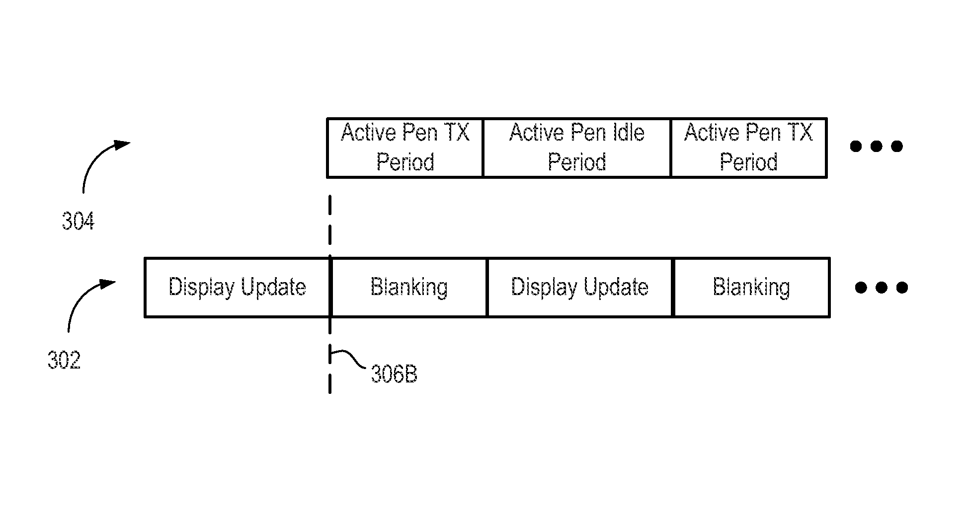
FIG. 3A illustrates a general relationship between display updating and active pen transmission.
FIG. 3B illustrates an aligned relationship between display updating and active pen transmission.
FIG. 4 is a block diagram illustrating the processing system in more detail according to embodiments.
FIG. 5 is a block diagram depicting another capacitive sensor device according to embodiments.
FIG. 6 is a flow diagram depicting a method of operating an input device integrated with a display according to embodiments.
To facilitate understanding, identical reference numerals have been used, where possible, to designate identical elements that are common to the figures. It is contemplated that elements of one embodiment may be beneficially incorporated in other embodiments.
DETAILED DESCRIPTION
The following detailed description is merely exemplary in nature and is not intended to limit the embodiments or the application and uses of such embodiments. Furthermore, there is no intention to be bound by any expressed or implied theory presented in the preceding technical field, background, brief summary or the following detailed description.
Turning now to the figures, FIG. 1 is a block diagram of an exemplary input device 100, in accordance with embodiments of the invention. The input device 100 may be configured to provide input to an electronic system (not shown). As used in this document, the term "electronic system" (or "electronic device") broadly refers to any system capable of electronically processing information. Some non-limiting examples of electronic systems include personal computers of all sizes and shapes, such as desktop computers, laptop computers, netbook computers, tablets, web browsers, e-book readers, and personal digital assistants (PDAs). Additional example electronic systems include composite input devices, such as physical keyboards that include input device 100 and separate joysticks or key switches. Further example electronic systems include peripherals such as data input devices (including remote controls and mice), and data output devices (including display screens and printers). Other examples include remote terminals, kiosks, and video game machines (e.g., video game consoles, portable gaming devices, and the like). Other examples include communication devices (including cellular phones, such as smart phones), and media devices (including recorders, editors, and players such as televisions, set-top boxes, music players, digital photo frames, and digital cameras). Additionally, the electronic system could be a host or a slave to the input device.
The input device 100 can be implemented as a physical part of the electronic system, or can be physically separate from the electronic system. As appropriate, the input device 100 may communicate with parts of the electronic system using any one or more of the following: buses, networks, and other wired or wireless interconnections. Examples include I.sup.2C, SPI, PS/2, Universal Serial Bus (USB), Bluetooth, RF, and IRDA.
In FIG. 1, the input device 100 is shown as a proximity sensor device (also often referred to as a "touchpad" or a "touch sensor device") configured to sense input provided by one or more input objects 140 in a sensing region 120. Example input objects include fingers and styli, as shown in FIG. 1.
Sensing region 120 encompasses any space above, around, in and/or near the input device 100 in which the input device 100 is able to detect user input (e.g., user input provided by one or more input objects 140). The sizes, shapes, and locations of particular sensing regions may vary widely from embodiment to embodiment. In some embodiments, the sensing region 120 extends from a surface of the input device 100 in one or more directions into space until signal-to-noise ratios prevent sufficiently accurate object detection. The distance to which this sensing region 120 extends in a particular direction, in various embodiments, may be on the order of less than a millimeter, millimeters, centimeters, or more, and may vary significantly with the type of sensing technology used and the accuracy desired. Thus, some embodiments sense input that comprises no contact with any surfaces of the input device 100, contact with an input surface (e.g. a touch surface) of the input device 100, contact with an input surface of the input device 100 coupled with some amount of applied force or pressure, and/or a combination thereof. In various embodiments, input surfaces may be provided by surfaces of casings within which the sensor electrodes reside, by face sheets applied over the sensor electrodes or any casings, etc. In some embodiments, the sensing region 120 has a rectangular shape when projected onto an input surface of the input device 100.
The input device 100 may utilize any combination of sensor components and sensing technologies to detect user input in the sensing region 120. The input device 100 comprises one or more sensing elements for detecting user input. As several non-limiting examples, the input device 100 may use capacitive, elastive, resistive, inductive, magnetic, acoustic, ultrasonic, and/or optical techniques.
Some implementations are configured to provide images that span one, two, three, or higher dimensional spaces. Some implementations are configured to provide projections of input along particular axes or planes.
In some capacitive implementations of the input device 100, voltage or current is applied to create an electric field. Nearby input objects cause changes in the electric field, and produce detectable changes in capacitive coupling that may be detected as changes in voltage, current, or the like.
Some capacitive implementations utilize arrays or other regular or irregular patterns of capacitive sensing elements to create electric fields. In some capacitive implementations, separate sensing elements may be ohmically shorted together to form larger sensor electrodes. Some capacitive implementations utilize resistive sheets, which may be uniformly resistive.
Some capacitive implementations utilize "self capacitance" (or "absolute capacitance") sensing methods based on changes in the capacitive coupling between sensor electrodes and an input object. In various embodiments, an input object near the sensor electrodes alters the electric field near the sensor electrodes, thus changing the measured capacitive coupling. In one implementation, an absolute capacitance sensing method operates by modulating sensor electrodes with respect to a reference voltage (e.g. system ground), and by detecting the capacitive coupling between the sensor electrodes and input objects.
Some capacitive implementations utilize "mutual capacitance" (or "transcapacitance") sensing methods based on changes in the capacitive coupling between sensor electrodes. In various embodiments, an input object near the sensor electrodes alters the electric field between the sensor electrodes, thus changing the measured capacitive coupling. In one implementation, a transcapacitive sensing method operates by detecting the capacitive coupling between one or more transmitter sensor electrodes (also "transmitter electrodes" or "transmitters") and one or more receiver sensor electrodes (also "receiver electrodes" or "receivers"). Transmitter sensor electrodes may be modulated relative to a reference voltage (e.g., system ground) to transmit transmitter signals. Receiver sensor electrodes may be held substantially constant relative to the reference voltage to facilitate receipt of resulting signals. A resulting signal may comprise effect(s) corresponding to one or more transmitter signals, and/or to one or more sources of environmental interference (e.g. other electromagnetic signals). Sensor electrodes may be dedicated transmitters or receivers, or may be configured to both transmit and receive.
In FIG. 1, a processing system 110 is shown as part of the input device 100. The processing system 110 is configured to operate the hardware of the input device 100 to detect input in the sensing region 120. The processing system 110 comprises parts of or all of one or more integrated circuits (ICs) and/or other circuitry components. For example, a processing system for a mutual capacitance sensor device may comprise transmitter circuitry configured to transmit signals with transmitter sensor electrodes, and/or receiver circuitry configured to receive signals with receiver sensor electrodes). In some embodiments, the processing system 110 also comprises electronically-readable instructions, such as firmware code, software code, and/or the like. In some embodiments, components composing the processing system 110 are located together, such as near sensing element(s) of the input device 100. In other embodiments, components of processing system 110 are physically separate with one or more components close to sensing element(s) of input device 100, and one or more components elsewhere. For example, the input device 100 may be a peripheral coupled to a desktop computer, and the processing system 110 may comprise software configured to run on a central processing unit of the desktop computer and one or more ICs (perhaps with associated firmware) separate from the central processing unit. As another example, the input device 100 may be physically integrated in a phone, and the processing system 110 may comprise circuits and firmware that are part of a main processor of the phone. In some embodiments, the processing system 110 is dedicated to implementing the input device 100. In other embodiments, the processing system 110 also performs other functions, such as operating display screens, driving haptic actuators, etc.
The processing system 110 may be implemented as a set of modules that handle different functions of the processing system 110. Each module may comprise circuitry that is a part of the processing system 110, firmware, software, or a combination thereof. In various embodiments, different combinations of modules may be used. Example modules include hardware operation modules for operating hardware such as sensor electrodes and display screens, data processing modules for processing data such as sensor signals and positional information, and reporting modules for reporting information. Further example modules include sensor operation modules configured to operate sensing element(s) to detect input, identification modules configured to identify gestures such as mode changing gestures, and mode changing modules for changing operation modes.
In some embodiments, the processing system 110 responds to user input (or lack of user input) in the sensing region 120 directly by causing one or more actions. Example actions include changing operation modes, as well as GUI actions such as cursor movement, selection, menu navigation, and other functions. In some embodiments, the processing system 110 provides information about the input (or lack of input) to some part of the electronic system (e.g. to a central processing system of the electronic system that is separate from the processing system 110, if such a separate central processing system exists). In some embodiments, some part of the electronic system processes information received from the processing system 110 to act on user input, such as to facilitate a full range of actions, including mode changing actions and GUI actions.
For example, in some embodiments, the processing system 110 operates the sensing element(s) of the input device 100 to produce electrical signals indicative of input (or lack of input) in the sensing region 120. The processing system 110 may perform any appropriate amount of processing on the electrical signals in producing the information provided to the electronic system. For example, the processing system 110 may digitize analog electrical signals obtained from the sensor electrodes. As another example, the processing system 110 may perform filtering or other signal conditioning. As yet another example, the processing system 110 may subtract or otherwise account for a baseline, such that the information reflects a difference between the electrical signals and the baseline. As yet further examples, the processing system 110 may determine positional information, recognize inputs as commands, recognize handwriting, and the like.
"Positional information" as used herein broadly encompasses absolute position, relative position, velocity, acceleration, and other types of spatial information. Exemplary "zero-dimensional" positional information includes near/far or contact/no contact information. Exemplary "one-dimensional" positional information includes positions along an axis. Exemplary "two-dimensional" positional information includes motions in a plane. Exemplary "three-dimensional" positional information includes instantaneous or average velocities in space. Further examples include other representations of spatial information. Historical data regarding one or more types of positional information may also be determined and/or stored, including, for example, historical data that tracks position, motion, or instantaneous velocity over time.
In some embodiments, the input device 100 is implemented with additional input components that are operated by the processing system 110 or by some other processing system. These additional input components may provide redundant functionality for input in the sensing region 120, or some other functionality. FIG. 1 shows buttons 130 near the sensing region 120 that can be used to facilitate selection of items using the input device 100. Other types of additional input components include sliders, balls, wheels, switches, and the like. Conversely, in some embodiments, the input device 100 may be implemented with no other input components.
In some embodiments, the input device 100 comprises a touch screen interface, and the sensing region 120 overlaps at least part of an active area of a display screen. For example, the input device 100 may comprise substantially transparent sensor electrodes overlaying the display screen and provide a touch screen interface for the associated electronic system. The display screen may be any type of dynamic display capable of displaying a visual interface to a user, and may include any type of light emitting diode (LED), organic LED (OLED), cathode ray tube (CRT), liquid crystal display (LCD), plasma, electroluminescence (EL), or other display technology. The input device 100 and the display screen may share physical elements. For example, some embodiments may utilize some of the same electrical components for displaying and sensing. As another example, the display screen may be operated in part or in total by the processing system 110.
It should be understood that while many embodiments of the invention are described in the context of a fully functioning apparatus, the mechanisms of the present invention are capable of being distributed as a program product (e.g., software) in a variety of forms. For example, the mechanisms of the present invention may be implemented and distributed as a software program on information bearing media that are readable by electronic processors (e.g., non-transitory computer-readable and/or recordable/writable information bearing media readable by the processing system 110). Additionally, the embodiments of the present invention apply equally regardless of the particular type of medium used to carry out the distribution. Examples of non-transitory, electronically readable media include various discs, memory sticks, memory cards, memory modules, and the like. Electronically readable media may be based on flash, optical, magnetic, holographic, or any other storage technology.
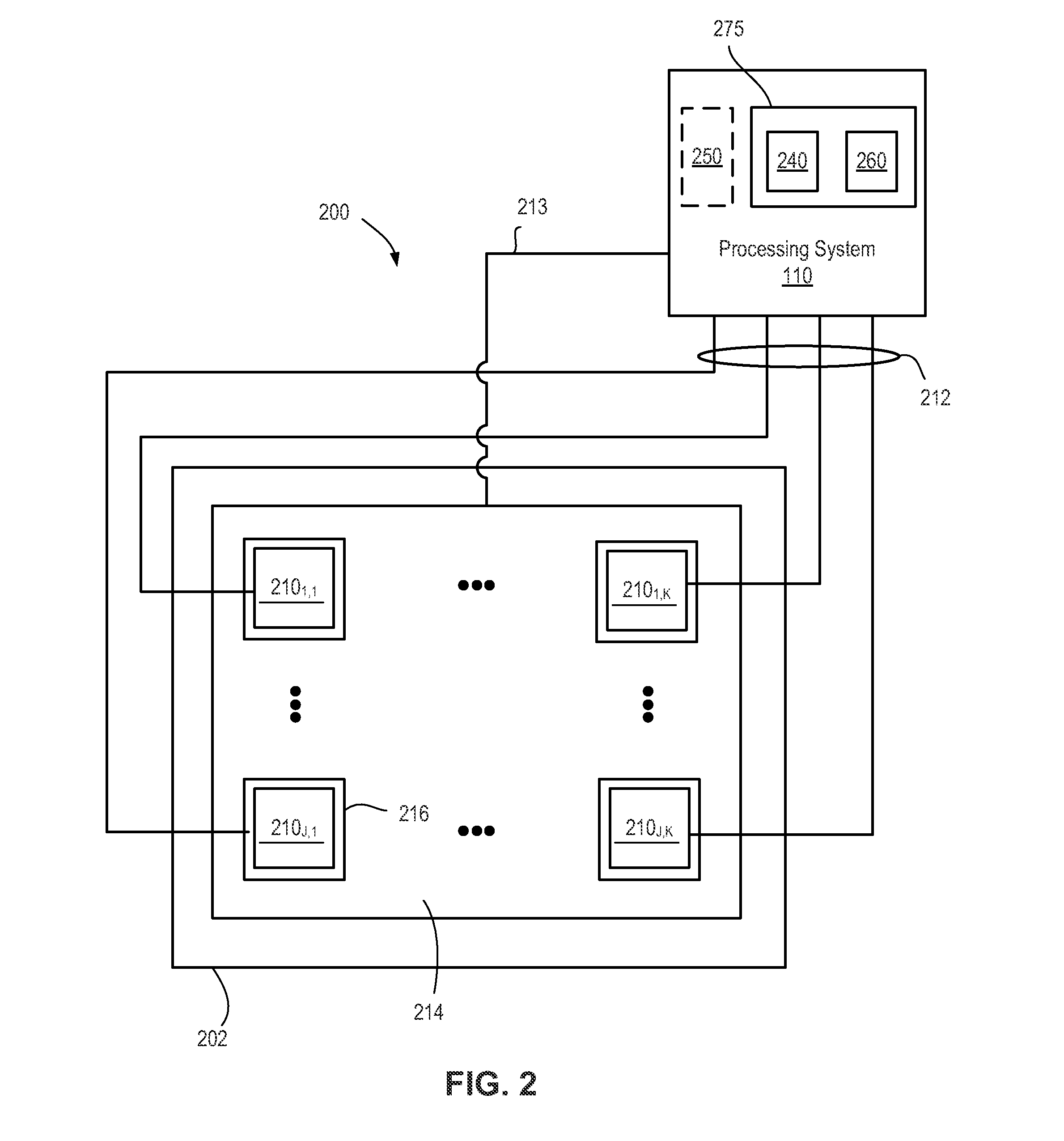
FIG. 2 is a block diagram depicting a capacitive sensor device 200 according to embodiments. The capacitive sensor device 200 comprises an example implementation of the input device 100 shown in FIG. 1. The capacitive sensor device 200 includes sensor electrodes disposed on a substrate 202. In the present example, the sensor electrodes comprise a plurality of sensor electrodes 210.sub.1,1 through 210.sub.J,K, where J and K are integers, and a grid electrode 214. The sensor electrodes 210 are ohmically isolated from each other and the grid electrode 214. The sensor electrodes 210 can be separated from the grid electrode 214 by a gap 216. In the present example, the sensor electrodes 210 are arranged in a rectangular matrix pattern, where at least one of J or K is greater than zero. The sensor electrodes 210 can be arranged in other patterns, such as polar arrays, repeating patterns, non-repeating patterns, or like type arrangements. The sensor electrodes 210 are coupled to the processing system 110 by conductive routing traces 212. In some examples, the grid electrode 214 can be coupled to the processing system 110 by a conductive routing trace 213.
In some examples, the sensor electrodes can be disposed on separate layers of the substrate 202. In other examples, the sensor electrodes can be disposed on a single layer of the substrate 202. While the sensor electrodes 210 and the grid electrode 214 are shown disposed on a single substrate 202, in some embodiments, the electrodes of the capacitive sensor device 200 can be disposed on more than one substrate. For example, some sensor electrodes can be disposed on a first substrate, other sensor electrodes can be disposed on a second substrate adhered to the first substrate, and the grid electrode can be disposed on the first, second, and/or yet another substrate. The sensor electrodes 210 can have the same or different widths, sizes and/or shapes. While the grid electrode 214 is shown as a single electrode, in some examples, the grid electrode 214 can be divided into a plurality of segments.
In a first mode of operation, the processing system 110 can operate the sensor electrodes to detect the presence of input object(s) 140 via absolute sensing techniques. That is, the processing system 110 is configured to operate the sensor electrodes to measure self-capacitance and changes thereof over time. The processing system 110 can determine position of the input object(s) 140 based changes in self-capacitance (absolute sensing).
In a second mode of operation, the processing system 110 can operate the sensor electrodes to detect presence of input object(s) 140 via transcapacitive sensing techniques. That is, the sensor electrodes 210 can be split into groups of transmitter and receiver electrodes. The processing system 110 can drive transmitter electrodes with transmitter signals and receive resulting signals from receiver electrodes. The resulting signals comprise effects of input object(s) 140. The processing system 110 measures mutual capacitance and changes thereof over time from the resulting signals. The processing system 110 can determine position of the input object(s) 140 based on changes in mutual capacitance (transcapacitive sensing).
In a third mode of operation, the processing system 110 can operate the sensor electrodes to detect presence of an input object 140 comprising an active pen. An active pen transmits a signal ("active pen signal"). The active pen signal can be a modulated signal having a particular frequency, phase, amplitude, shape, etc. In some embodiments, the active pen periodically transmits the active pen signal according to a particular duty cycle. In a transmission period, the active pen transmits the active pen signal. In an idle period, the active pen does not transmit the active pen signal. The active pen signal is received by the sensor electrodes of the capacitive sensor device 200. The processing system 110 measures changes in the resulting signals, which comprise effects corresponding to the active pen signal and can determine position of the active pen based on such changes in capacitance.
The capacitive sensor device 200 can operate in any one of the modes described above. The capacitive sensor device 200 can also switch between any two or more of the modes described above. In one embodiment, the capacitive sensor device 200 can operate in multiple modes within an overlapping time period, for example, by performing capacitance sensing of input object(s) while performing sensing of an active pen.
In some embodiments, the capacitive sensor device 200 performs sensing periodically according to a particular duty cycle. During a sensing period, the processing system 100 can operate in any of the modes described above. During a non-sensing period, the processing system 110 may perform other operations (e.g., display updating) or may be idle. In some embodiments, described below, the capacitive sensor device 200 continuously senses an active pen in both the sensing and non-sensing periods.
The processing system 110 can include one or more modules, such as a sensor module 240 and a determination module 260. The sensor module 240 and the determination module 260 comprise modules that perform different functions of the processing system 110. In other examples, different configurations of modules can perform the functions described herein. The sensor module 240 and the determination module 260 can include sensor circuitry 270 and can also include firmware, software, or a combination thereof operating in cooperation with the sensor circuitry 270. In some embodiments, the processing system 110 can include a display driver module 250.
In an embodiment, the sensor module 240 includes sensor circuitry 275 that can excite or drive sensor electrodes with signals. The terms "excite" and "drive" as used herein encompasses controlling some electrical aspect of the driven element. For example, it is possible to drive current through a wire, drive charge into a conductor, drive a substantially constant or varying voltage waveform onto an electrode, etc. The sensor module 204 can drive a sensor electrode using a modulated signal generally having a shape, frequency, amplitude, and phase. The sensor module 204 can also measure some electrical aspect of a driven element indicative of capacitance (e.g., charge, voltage, current). The sensor module 204 can drive a sensor electrode and then measure changes of capacitive load on the sensor electrode (i.e., changes in absolute capacitance). The sensor module 204 can drive a transmitter electrode to transmit a transmitter signal and then measure changes in mutual capacitance from a resulting signal on a receiver electrode (i.e., changes in transcapacitance). The sensor module 204 can also hold sensor electrodes at a substantially constant voltage for detecting an active pen signal. The sensor module 204 can also receive an active pen signal while the sensor electrodes are modulated. The sensor module 204 can also drive one or more electrodes with a shield signal (e.g., a substantially constant voltage or varying voltage (guard signal)). In general, the sensor module 240 obtains capacitive sensing signals derived from operating the sensor electrodes for either transcapacitive sensing or absolute capacitive sensing.
The sensor module 240 generates measurements of some characteristic of the capacitive sensing signals, such as voltage, current, charge, or the like. The determination module 260 receives the measurements from the sensor module 240. The determination module 260 derives information from the measurements. For example, the determination module 260 can determine a baseline capacitance for the sensor electrode pattern, determine changes in mutual capacitance between sensor electrodes and/or changes in self-capacitance of sensor electrodes, and compare changes in capacitance with the baseline to detect object presence, position, motion, etc. The changes in capacitance can be associated with specific locations of the sensing region 120 to create a "capacitive image" or "capacitive frame." The changes in capacitance can be associated with a specific axis of the sensing region 120 to create a "capacitive profile" along that axis. When compensated with the baseline, the capacitive image(s) and/or capacitive profile(s) enable the sensing of contact, hovering, or other user input with respect to the formed sensing regions by the sensor electrode pattern. The determination module 260 can determine positional information, size, type, and the like of input object(s).
In some touch screen embodiments, one or more of the sensor electrodes on the substrate 202 comprise one or more display electrodes used in updating the display of a display screen. In one or more embodiments, the display electrodes comprise one or more segments of a Vcom electrode (common voltage electrode), a source drive line, gate line, an anode electrode or cathode electrode, or any other display element. These display electrodes may be disposed on an appropriate display screen substrate. For example, the display electrodes may be disposed on the a transparent substrate (a glass substrate, TFT glass, or any other transparent material) in some display screens (e.g., In Plane Switching (IPS) or Plane to Line Switching (PLS) Organic Light Emitting Diode (OLED)), on the bottom of the color filter glass of some display screens (e.g., Patterned Vertical Alignment (PVA) or Multi-domain Vertical Alignment (MVA)), over an emissive layer (OLED), etc. In such embodiments, the display electrode can also be referred to as a "combination electrode", since it performs multiple functions. The processing system 110 can include the display driver module 250 configured to drive electrodes on the substrate 202 for display updating. The display driver module 250 includes circuitry configured to provide display image update information to a display device during a display update period. Alternatively, the display driver module 250 can be in a device separate from the processing system 110 and coupled to the processing system 110.
In some embodiments, capacitive sensing and display updating occur during non-overlapping periods. Each cycle of the sensing period can occur between consecutive cycles of the display update period. During the display update period, display lines of a display frame are updated. A cycle of the sensing period can occur between display line updates, which may be referred to as a horizontal blanking period or h-blanking period. In some embodiments, the horizontal blanking period can be lengthened and referred to as a long horizontal blanking period, long h-blanking period, or distributed blanking period. The long h-blanking period can be at least as long as the display update period. In other embodiments, a cycle of the sensing period can occur between display frame updates, which may be referred to as a vertical blanking period or v-blanking period. The processing system 110 can operate sensor electrodes on the substrate 202 for capacitive sensing during any cycle of the sensing period. As described herein, the processing system 110 can also operate the sensor electrodes on the substrate 202 for sensing an active pen during any cycle of the sensing period or the display update period.
FIG. 3A illustrates a general relationship between display updating and active pen transmission. As noted above, an active pen can alternate between transmitting an active pen signal and not transmitting the active pen signal (e.g., idling). An active pen duty cycle 304 generally includes a transmission period and an idle period. During cycles of the transmission period, the active pen transmits the active pen signal. During cycles of the idle period, the active pen does not transmit the active pen signal. A display update duty cycle 302 generally includes a display update period and a blanking period (e.g., an h-blanking period or long h-blanking period, as shown). During cycles of the display update period, display lines are updated. During cycles of the blanking period, display lines are not updated. Also, during cycles of the blanking period, the processing system 110 can perform capacitive sensing. Thus, the sensing period can occur within the blanking period (e.g., the sensing period can be approximately equal to, or shorter than, the blanking period).
As shown in FIG. 3A, the active pen duty cycle 304 is asynchronous with the display update duty cycle 302. Generally, there is a phase difference 306A between the active pen transmission period and the blanking period. In a worst case, the phase difference 306A is such that the active pen transmission period occurs completely within the display update period. That is, the active pen is not transmitting during the blanking period. In such case, the active pen signal is not available for sensing by the processing system 110 during the sensing period within the blanking period. If the processing system 110 only sensed the active pen during the sensing period, the active pen would not be detected in this worst case scenario. In other cases, the phase difference 306A can be such that only a portion of the active pen transmission period occurs during the blanking period. While this may allow the processing system 110A to detect the active pen (depending on the length over the overlap), such portion is insufficient for sensing and tracking the active pen during the entire sensing period.
FIG. 3B illustrates an aligned relationship between display updating and active pen transmission. As shown in FIG. 3B, a phase difference 306B between the active pen transmission period and the blanking period is at or near zero. Thus, the active pen transmission period occurs within the blanking period and, accordingly, within the sensing period. The active pen transmission period can be equal to, longer, or shorter than the sensing period. If the active pen transmission period is at least equal to the sensing period, after alignment the processing system 110 can sense the active pen during the entire sensing period. If the active pen transmission period is shorter than the sensing period, after alignment the processing system 110 can sense the active pen during the entire active pen transmission period.
As described herein, to align the active pen transmission period and the display update period, the processing system 110 can monitor for the active pen signal in both the display update period and the blanking period of the display update duty cycle 302. The processing system 110 is also configured with knowledge of the length of the active pen transmission period. Upon detection of the active pen signal, the processing system 110 adjusts the phase difference between the active pen transmission period and the sensing period to be substantially aligned (e.g., as shown in FIG. 3B). For example, the processing system 110 can control a display driver module to adjust the blanking period to be aligned with the active pen transmission period. In examples described herein, the sensing period is assumed to begin at the start of the blanking period. Hence, alignment with the blanking period is substantially equivalent to alignment with the sensing period. If the sensing period begins some time after the blanking period, the active pen transmission period is aligned with the sensing period.
FIG. 4 is a block diagram illustrating the processing system 110 in more detail according to embodiments. The processing system 110 includes the sensor module 240. The sensor module 240 includes sensor circuitry such as an analog front end (AFE) 406 coupled to the grid electrode 214. The AFE 406 can include one or more integrators 408 coupled to the grid electrode 214. In some embodiments, the grid electrode 214 can include a plurality of segments 402. The segments 402 can be coupled to a single integrator 408 or individually to a plurality of integrators 408. The sensor module 240 includes a sensor electrode multiplexer (MUX) 404 coupled to the sensor electrodes 210. The sensor electrode MUX 404 is configured to couple the sensor electrodes 210 to integrators 412 in an AFE 410. The sensor electrode MUX 404 can be configured to couple any subset of the sensor electrodes 210 to any of the integrators 412, where a subset of sensor electrodes includes one or more of the sensor electrodes.
The integrator(s) 408 and the integrators 312 are configured to integrate some characteristic of the electrodes, such as charge, voltage, current, etc. over time. For example, the AFE 406 can couple a voltage to the grid electrode 214 and the integrator(s) 408 can integrate charge over time. Likewise, the AFE 406 can couple a voltage to the sensor electrodes 210 and the integrators 412 can integrate charge over time. The AFE 406 and the AFE 410 can sample, demodulate, filter, etc. the integrated signals output by the integrator(s) 408 and the integrators 412 to generate measurement signals.
The determination module 260 processes the measurement signals. The determination module 260 can process the measurement signals using absolute sensing, transcapacitive sensing, or active pen sensing to detect input object(s). The determination module 260 can control the sensor module 240 to generate the measurements of interest based on the current mode of operation. The determination module 260 can, in some embodiments, perform both input sensing (absolute or transcapacitive) and active pen sensing concurrently.
In an embodiment, the determination module 260 controls the AFE 406 to receive an active pen signal using the grid electrode 214. The determination module 260 can detect presence of an active pen based on the active pen signal received by the AFE 406. For example, the AFE 406 can receive the active pen signal by measuring current supplied to maintain the grid electrode 214 at a target voltage (e.g., a substantially constant voltage). For example, the target voltage can be Vcom (i.e., the common voltage of the display). When an active pen is transmitting an active pen signal, the active pen signal is capacitively coupled to the grid electrode 214. The AFE 406 supplies current to the grid electrode 214 to maintain the grid electrode 214 at the target voltage. The integrator(s) 408 integrate the supplied current over time. When the active pen is not transmitting the active pen signal, AFE 406 supplies a baseline current to the grid electrode 214. The determination module 260 can process measurements produced by the AFE 406 to detect changes from the baseline, which is indicative of the active pen signal.
If the grid electrode 214 is not segmented, the AFE 406 can be used to detect presence of the active pen signal. If the grid electrode 214 include segments 402, and the AFE 406 includes an integrator 408 coupled to each of the segments, measurements from the AFE 406 can be used to both detect presence of the active pen signal and to determine position of the active pen relative to the segments 402.
In an embodiment, the grid electrode 214 (or segments 402 thereof) is not used to update the display during the display update period. Thus, the determination module 260 can control the AFE 406 to receive the active pen signal during the display update period. The determination module 260 can also control the AFE 406 to receive the active pen signal during the sensing period. Touch sensing can be performed using the sensor electrodes 210, while active pen sensing is performed using the grid electrode 214 (or segments 402 thereof). In this manner, the determination module 260 can both perform touch sensing and active pen sensing concurrently. By detecting the active pen signal, the determination module 206 can determine the phase of the active pen duty cycle regardless of how the active pen transmission period is aligned with the blanking period (sensing period).
The determination module 260 can include a phase detector 414 to track the phase of the active pen duty cycle. The determination module 260 can adjust the sensing period for alignment with the transmission period of the active pen signal. In an embodiment, the display module 260 controls the display driver module 250 to adjust the blanking period to be substantially aligned with the active pen transmission period based on output of the phase detector 414.
In another embodiment, the determination module 260 can control the sensor module 240 to receive the active pen signal using a subset 403 of the sensor electrodes 210. In such embodiment, the sensor module 240 can be configured such that the sensor electrode MUX 404 is coupled to the AFE 406. The sensor electrode MUX 404 is configured to couple the electrode subset 403 to the AFE 406 for receiving the active pen signal. In such a configuration, the connection between the grid electrode 214 and the AFE 406 can be omitted. The AFE 406 can couple each sensor electrode in the selected subset 403 to an integrator 408. Measurements from the AFE 406 can be used to both detect presence of the active pen signal and to determine position of the active pen relative to the electrode subset 403 used to receive the active pen signal.
For example, the AFE 406 can receive the active pen signal by measuring current supplied to maintain the selected electrode subset 403 at a target voltage (e.g., a substantially constant voltage). For example, the target voltage can be Vcom. When an active pen is transmitting an active pen signal, the active pen signal is capacitively coupled to the selected electrode subset 403. The AFE 406 supplies current to the selected electrode subset 403 to maintain them at the target voltage. The integrators 408 integrate the supplied current over time. When the active pen is not transmitting the active pen signal, AFE 406 supplies a baseline current to the selected electrode subset 403. The determination module 260 can process measurements produced by the AFE 406 to detect changes from the baseline, which is indicative of the active pen signal.
In an embodiment, the selected electrode subset 403 is not used to update the display during the display update period. Thus, the determination module 260 can control the AFE 406 to receive the active pen signal during the display update period. The determination module 260 can also control the AFE 406 to receive the active pen signal during the sensing period. Touch sensing can be performed using those sensor electrodes 210 other than the selected electrode subset 403. In this manner, the determination module 260 can both perform touch sensing and active pen sensing concurrently. Thus, the determination module 206 can determine the phase of the active pen duty cycle regardless of how the active pen transmission period is aligned with the blanking period (sensing period).
In an embodiment, the selected electrode subset 403 used to receive the active pen signal comprises a static spatial arrangement of the sensor electrodes 210. For example, a checker-board pattern or the like can be employed. Alternatively, the determination module 260 can dynamically select the electrode subset 403 used to receive the active pen signal. For example, different subsets can be selected as the active pen moves through the sensing area.
FIG. 5 is a block diagram depicting another capacitive sensor device 200A according to embodiments. The capacitive sensor device 200A comprises an example implementation of the input device 100 shown in FIG. 1. The capacitive sensor device 200A includes sensor electrodes disposed on the substrate 202. In the present example, the sensor electrodes include two pluralities of sensor electrodes 520-1 through 520-n (collectively "sensor electrodes 520"), and 530-1 through 530-m (collectively "sensor electrodes 530"), where m and n are integers greater than zero. The sensor electrodes 520 and 530 are separated by a dielectric (not shown).
In some examples, the sensor electrodes 520 and the sensor electrodes 530 can be disposed on separate layers of the substrate 202. In other examples, the sensor electrodes 520 and the sensor electrodes 530 can be disposed on a single layer of the substrate 202. While the sensor electrodes are shown disposed on a single substrate 202, in some embodiments, the sensor electrodes can be disposed on more than one substrate. For example, some sensor electrodes can be disposed on a first substrate, and other sensor electrodes can be disposed on a second substrate adhered to the first substrate. The sensor electrodes 520, 530 can have the same or different widths, sizes and/or shapes.
In the present example, the sensor electrode pattern is shown with the sensor electrodes 520, 530 arranged in an x/y grid of bars and strips. It is to be understood that the sensor electrode pattern is not limited to such bars and stripes arrangement, but instead can include numerous sensor patterns. For example, the sensor electrodes on the substrate 202 can be arranged in a matrix pattern of sensor electrodes surrounded by a grid electrode. Although the sensor electrode pattern is depicted as rectangular, the sensor electrode pattern can have other shapes, such as a circular shape.
The sensor electrodes 520 and 530 are coupled to the processing system 110 by conductive routing traces 504, 506. When in operation, the processing system 110 is coupled to the sensor electrodes 520, 530 through the conductive routing traces 504, 506 to implement the sensing region 120 for sensing inputs. In an embodiment, each set of sensor electrodes can have a dedicated function. For example, the sensor electrodes 530 can transmit transmitter signals generated by the processing system 110 or another device under control of the processing system 110. The processing system 110 can receive resulting signals with the sensor electrodes 520. In such an embodiment, the sensor electrodes 530 are "transmitter electrodes" and the sensor electrodes 520 are "receiver electrodes." In some embodiments, one or more of the sensor electrodes 520 may be measured to sense self-capacitance (absolute capacitance). In another embodiment, the sets of sensor electrodes do not have a dedicated function (undifferentiated electrodes) and the sensor electrodes 530 can function as either transmitter electrodes or receiver electrodes, and the sensor electrodes 520 can function as either receiver electrodes or transmitter electrodes.
In some embodiments, the determination module 260 can control the sensor module 240 to receive an active pen signal using the sensor electrodes 520 in a manner similar to receiving the active pen signal using the grid electrode 214 (or segments thereof) and the selected subset of sensor electrodes 210. In an embodiment, the sensor electrodes 520 can include receiver electrodes that are not used to update a display during the display update period. In other embodiments, the determination module 260 can control the sensor module 240 to receive an active pen signal using the sensor electrodes 530 (e.g., transmitter electrodes not used to update a display during the display update period).
FIG. 6 is a flow diagram depicting a method 600 of operating an input device integrated with a display according to embodiments. The method 600 can be performed by the capacitive sensor device 200 or the capacitive sensor device 200A described above. The method 600 begins at step 602, where the processing system 110 receives an active pen signal with designated sensor electrode(s). In an embodiment, the designated sensor electrode(s) include a grid electrode 214 or segments 402 of a grid electrode 214 disposed between sensor electrodes 210. In another embodiment, the designated sensor electrode(s) include a selected subset of the sensor electrodes 210 circumscribed by the grid electrode 214. In another embodiment, the designated sensor electrode(s) include a selected set of sensor electrodes in bars and stripes type sensor (e.g., FIG. 5), such as the receiver electrodes 520 or the transmitter electrodes 530. The active pen signal can be received during a display update period, during a sensing period, or both. The active pen signal can be received using designated sensor electrode(s) not used to update a display. The active pen signal can be received concurrently with touch sensing using other sensor electrodes.
At step 604, the processing system 110 adjusts the sensing period of the input device for alignment with a transmission period of the active pen signal. This allows the processing system 110 to sense the entire active pen transmission period during the sensing period, or sense the active pen transmission during the entire sensing period (depending on which is longer). In an embodiment, the processing system 110 controls a display driver module (e.g., the display driver module 250 within the processing system 110 or an external display driver module) to adjust the blanking period to be aligned with the active pen transmission period.
Thus, the embodiments and examples set forth herein were presented in order to best explain the present invention and its particular application and to thereby enable those skilled in the art to make and use the invention. However, those skilled in the art will recognize that the foregoing description and examples have been presented for the purposes of illustration and example only. The description as set forth is not intended to be exhaustive or to limit the invention to the precise form disclosed.
* * * * *
References
D00000
D00001
D00002
D00003
D00004
D00005
D00006
XML
uspto.report is an independent third-party trademark research tool that is not affiliated, endorsed, or sponsored by the United States Patent and Trademark Office (USPTO) or any other governmental organization. The information provided by uspto.report is based on publicly available data at the time of writing and is intended for informational purposes only.
While we strive to provide accurate and up-to-date information, we do not guarantee the accuracy, completeness, reliability, or suitability of the information displayed on this site. The use of this site is at your own risk. Any reliance you place on such information is therefore strictly at your own risk.
All official trademark data, including owner information, should be verified by visiting the official USPTO website at www.uspto.gov. This site is not intended to replace professional legal advice and should not be used as a substitute for consulting with a legal professional who is knowledgeable about trademark law.