Active Stylus
HARLEY; Jonah A. ; et al.
U.S. patent application number 13/166726 was filed with the patent office on 2012-12-27 for active stylus. Invention is credited to Jonah A. HARLEY, David I. Simon.
| Application Number | 20120327041 13/166726 |
| Document ID | / |
| Family ID | 46601883 |
| Filed Date | 2012-12-27 |


| United States Patent Application | 20120327041 |
| Kind Code | A1 |
| HARLEY; Jonah A. ; et al. | December 27, 2012 |
ACTIVE STYLUS
Abstract
An active stylus is disclosed. The stylus includes an electrode at a tip of the stylus; and powered circuitry coupled to the electrode and configured for capacitively coupling the electrode with a capacitive touch sensor panel. The powered circuitry can further include drive circuitry configured to output a drive voltage at the electrode and/or sense circuitry configured to sense a voltage received at the electrode.
| Inventors: | HARLEY; Jonah A.; (Mountain View, CA) ; Simon; David I.; (San Francisco, CA) |
| Family ID: | 46601883 |
| Appl. No.: | 13/166726 |
| Filed: | June 22, 2011 |
| Current U.S. Class: | 345/179 |
| Current CPC Class: | G06F 3/0442 20190501; G06F 3/03545 20130101; G06F 3/0383 20130101; G06F 2203/04112 20130101; G06F 3/0446 20190501; G06F 3/0441 20190501; G06F 3/0445 20190501 |
| Class at Publication: | 345/179 |
| International Class: | G06F 3/033 20060101 G06F003/033 |
Claims
1. An active stylus, comprising: an electrode at a tip of the stylus; and powered circuitry coupled to the electrode and configured for capacitively coupling the electrode with a capacitive touch sensor panel.
2. The active stylus of claim 1, wherein the powered circuitry comprises: drive circuitry configured to output a drive voltage at the electrode.
3. The active stylus of claim 1, further comprising a power source coupled to the powered circuitry for supplying power to the powered circuitry.
4. The active stylus of claim 2, wherein the drive circuitry further comprises: a clock to generate a drive voltage; a microcontroller connected to the clock and configured to control the drive voltage; and an amplifier connected to the microcontroller and configured to adjust the drive voltage.
5. The active stylus of claim 1, wherein the powered circuitry comprises: sense circuitry configured to sense a voltage received at the electrode.
6. The active stylus of claim 5, the sense circuitry further comprising an amplifier to adjust the sensed voltage.
7. The active stylus of claim 6, wherein the sense circuitry further comprises: a clock to generate a demodulation signal; a phase shifter to shift the phase of the demodulation signal; and a set of mixers to receive the sensed voltage and either the demodulation signal or the phase-shifted demodulation signal to demodulate the sensed voltage.
8. The active stylus of claim 7, wherein the mixer receiving the demodulation signal produces an in-phase component; wherein the mixer receiving the phase-shifted demodulation signal produces a quadrature component; and wherein the in-phase component and the quadrature component are combined to determine an amplitude proportional to a capacitance formed by the electrode.
9. The active stylus of claim 1, the active stylus incorporated into a touch-based input system, the system comprising: a capacitive touch sensor panel including a plurality of sense lines; and one or more sense channels coupled to the plurality of sense lines, the one or more sense channels configured for detecting a change in capacitance between the electrode and one or more sense lines to determine a location of a touch by the active stylus on the touch sensor panel.
10. The active stylus of claim 9, wherein the electrode is stimulated at a frequency to identify the presence of the stylus.
11. The active stylus of claim 8, wherein the electrode is stimulated with a pattern that identifies a presence of the stylus.
12. The active stylus of claim 9, wherein the one or more sense channels comprise at least one row channel and at least one column channel.
13. The active stylus of claim 9, wherein the active stylus further comprises: a clock to generate a drive voltage; a microcontroller connected to the clock and configured to control the drive voltage; and an amplifier connected to the microcontroller and configured to adjust the drive voltage.
14. The active stylus of claim 9, wherein one or more sense channels comprise: a sense amplifier to adjust a detected change in capacitive coupling; a clock to generate a demodulation signal; a phase shifter to shift a phase of the demodulation signal; and a set of mixers to receive the detected change in capacitive coupling and either the demodulation signal or the phase-shifted demodulation signal to demodulate the sensed voltage.
15. The active stylus of claim 14, wherein the mixer receiving the demodulation signal produces an in-phase component; wherein the mixer receiving the phase-shifted demodulation signal produces a quadrature component; and wherein the in-phase component and the quadrature component are combined to determine an amplitude proportional to a capacitance formed by the drive channel and the sense channel.
16. The active stylus of claim 9, wherein the capacitive touch sensor panel is in communication with the stylus via one of a physical cable and a wireless channel.
17. The active stylus of claim 9, wherein the capacitive touch sensor panel further comprises at least one drive line configured to generate a signal that can be sensed by at least one of the sense channels.
18. The active stylus of claim 5, the active stylus incorporated into a touch-based input system, the system comprising: a capacitive touch sensor panel including a plurality of drive lines; and one or more drive channels coupled to the plurality of drive lines, wherein an identity of a drive line being stimulated by a drive channel is used to determine a location of a touch by the active stylus on the touch sensor panel.
19. The active stylus of claim 18, wherein the stylus further comprises an amplifier to adjust the sensed voltage.
20. The active stylus of claim 19, wherein the stylus further comprises: a clock to generate a demodulation signal; a phase shifter to shift the phase of the demodulation signal; and a set of mixers to receive the sensed voltage and either the demodulation signal or the phase-shifted demodulation signal to demodulate the sensed signal.
21. The active stylus of claim 20, wherein the mixer receiving the demodulation signal produces an in-phase component; wherein the mixer receiving the phase-shifted demodulation signal produces a quadrature component; and wherein the in-phase component and the quadrature component are combined to determine an amplitude proportional to a capacitance formed by a drive channel and the electrode.
22. The active stylus of claim 18, wherein the capacitive touch sensor panel is in communication with the stylus via one of a physical cable and a wireless channel.
23. The active stylus of claim 18, wherein a signal from each of the drive channels can be distinguished by a unique code.
24. A stylus touch detection method, comprising: capacitively coupling a powered electrode in the stylus with a touch sensor panel by forming a mutual capacitance between the electrode and the touch sensor panel to detect a stylus touch on the touch sensor panel.
25. The method of claim 24, further comprising: generating a stimulation signal at the powered electrode; and detecting the stylus touch on the touch sensor panel upon detection of a capacitively coupled stimulation signal on a sense line in the touch sensor panel.
26. The method of claim 25, further comprising: generating a stimulation signal in the touch sensor panel; and detecting the stylus touch on the touch sensor panel upon detection of a capacitively coupled stimulation signal on a sense circuit in the stylus.
Description
FIELD
[0001] This relates generally to touch sensing, and more particularly, to providing a stylus that can act as a drive and/or sense element in a capacitive touch system.
BACKGROUND
[0002] Many types of input devices are available for performing operations in a computing system, such as buttons or keys, mice, trackballs, touch sensor panels, joysticks, touch pads, touch screens, and the like. Touch sensitive devices, and touch screens, in particular, are becoming increasingly popular because of their ease and versatility of operation as well as their declining price. Touch sensitive devices can include a touch sensor panel, which can be a clear panel with a touch sensitive surface, and a display device such as a liquid crystal display (LCD) that can be positioned partially or fully behind the panel, or integrated with the panel, so that the touch sensitive surface can substantially cover the viewable area of the display device. Touch sensitive devices can generally allow a user to perform various functions by touching or hovering over the touch sensor panel using one or more fingers, a stylus or other object at a location often dictated by a user interface (UI) including virtual buttons, keys, bars, displays, and other elements, being displayed by the display device. In general, touch screens can recognize a touch event and the position of the touch event on the touch sensor panel or a hover event and the position of the hover event on the touch sensor panel, and the computing system can then interpret the touch or hover event in accordance with the display appearing at the time of the event, and thereafter can perform one or more operations based on the event.
[0003] Touch screens can allow a user to perform various functions by touching the touch sensor panel using a finger, stylus or other object. More advanced touch screens are capable of detecting multiple touches simultaneously. In general, touch screens can recognize the position of the one or more touches on the touch sensor panel, and a computing system can then interpret the touches, either individually or as a single gesture in accordance with the display appearing at the time of the touch event, and thereafter can perform one or more actions based on the touch event.
[0004] When a stylus has been used as an input device in a capacitive touch system, the stylus has traditionally been finger-like in nature. A conventional stylus is often simply a conductive rod with a finger-sized rounded tip large enough to disrupt the electric field lines between the drive and sense electrodes of a capacitive touch sensor panel. As such, conventional styluses are passive input devices in that they are incapable of actively transmitting stimulus signals or sensing a touch-induced capacitance change in a capacitive touch sensor panel.
SUMMARY
[0005] This generally relates to a stylus that can act as a drive and/or a sense element in a capacitive touch system. Unlike conventional styluses which work passively by blocking electric field lines between the drive and sense electrodes of a capacitive touch sensor panel, the styluses disclosed in the various embodiments of this disclosure can either act as a drive electrode to create an electric field between the drive electrode and the sense lines of a mutual capacitive touch sensor panel, or as a sense electrode for sensing capacitively coupled signals from one or more stimulated drive rows and columns of the touch sensor panel or both. Accordingly, the styluses disclosed herein can be referred to as active styluses in comparison to conventional passive styluses. These active styluses can significantly improve stylus sensing on a mutual capacitive touch sensor panel without incurring significant additional cost.
BRIEF DESCRIPTION OF THE DRAWINGS
[0006] FIG. 1a illustrates the underlying structure of an exemplary capacitive touch sensor panel.
[0007] FIGS. 1b and 1c illustrate the capacitive touch sensor panel of FIG. 1a interacting with an exemplary passive stylus.
[0008] FIG. 2 illustrates an exemplary active stylus for use with a capacitive touch sensor panel according to various embodiments.
[0009] FIG. 3 illustrates exemplary drive circuitry of the active stylus of FIG. 2 according to various embodiments.
[0010] FIG. 4 illustrates the structure of an exemplary capacitive touch sensor panel according to various embodiments.
[0011] FIG. 5 illustrates the interaction between the active stylus of FIG. 2 with the touch sensor panel of FIG. 4 according to various embodiments.
[0012] FIG. 6 illustrates exemplary sense circuitry of the touch sensor panel of FIG. 4 according to various embodiments.
[0013] FIG. 7 illustrates another exemplary active stylus for use with a capacitive touch sensor panel according to various embodiments.
[0014] FIG. 8 illustrates exemplary sense circuitry of the active stylus of FIG. 7 according to various embodiments.
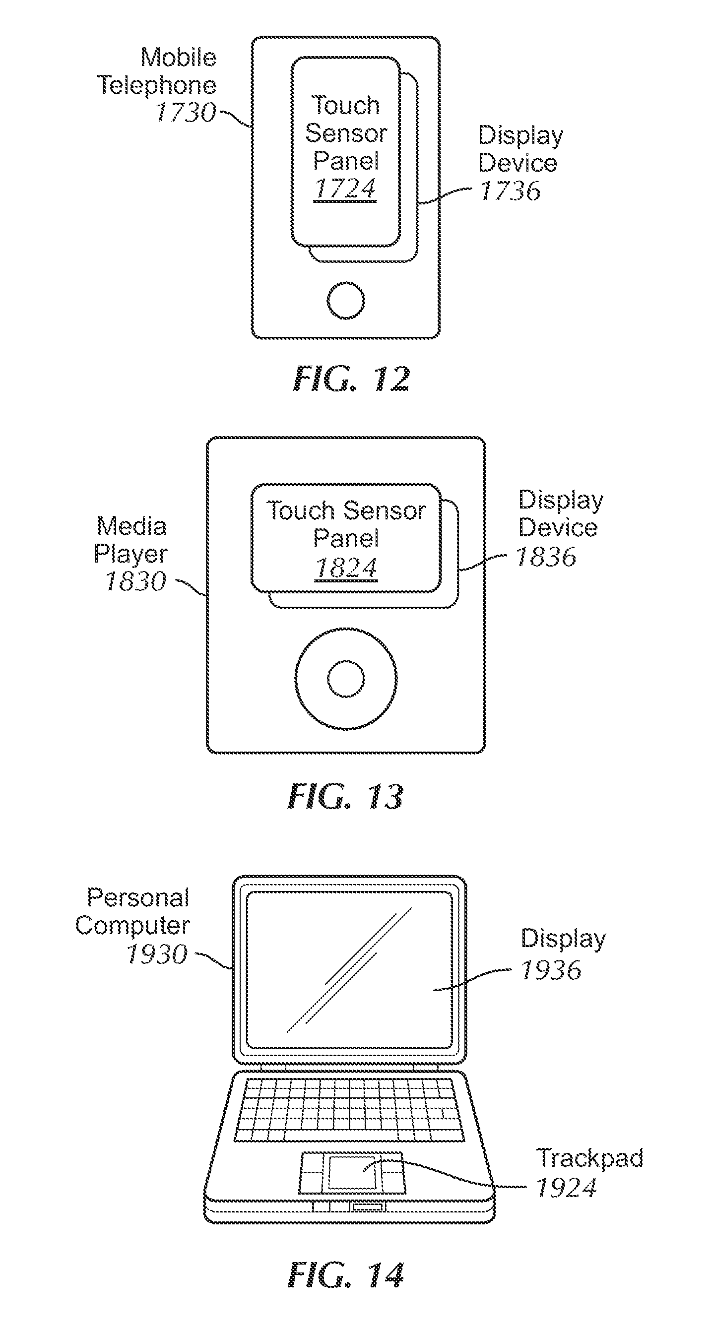
[0015] FIG. 9 illustrates the structure of another exemplary touch sensor panel according to various embodiments.
[0016] FIG. 10 illustrates the interaction between the active stylus of FIG. 7 with the touch sensor panel of FIG. 9 according to various embodiments.
[0017] FIG. 11 illustrates an exemplary computing system for use with a stylus according to various embodiments.
[0018] FIG. 12 illustrates an exemplary mobile telephone for use with a stylus according to various embodiments.
[0019] FIG. 13 illustrates an exemplary digital media player for use with a stylus according to various embodiments.
[0020] FIG. 14 illustrates an exemplary personal computer for use with a stylus according to various embodiments.
DETAILED DESCRIPTION
[0021] In the following description of example embodiments, reference is made to the accompanying drawings in which it is shown by way of illustration specific embodiments that can be practiced. It is to be understood that other embodiments can be used and structural changes can be made without departing from the scope of the various embodiments.
[0022] This generally relates to a stylus that can act as a drive and/or a sense element in a capacitive touch system. Unlike conventional styluses which work passively by blocking electric field lines between the drive and sense electrodes of a capacitive touch sensor panel, the styluses disclosed in the various embodiments of this disclosure can either act as a drive electrode to create an electric field between the drive electrode and the sense lines of a mutual capacitive touch sensor panel, or as a sense electrode for sensing capacitively coupled signals from one or more stimulated drive rows and columns of the touch sensor panel or both. Accordingly, the styluses disclosed herein can be referred to as active styluses in comparison to conventional passive styluses. These active styluses can significantly improve stylus sensing on a mutual capacitive touch sensor panel without incurring significant additional cost.
[0023] In the following paragraphs, a brief description of the structure of a typical capacitive touch sensor panel and its interaction with a conventional passive stylus is first discussed before the various exemplary embodiments of the disclosure are introduced.
[0024] Capacitive touch sensor panels are well known in the art and have been widely adopted in various types of electronic devices, such as tablet PCs (e.g., the iPad.RTM. from Apple Inc. of Cupertino, Calif.) and smartphones (e.g., the iPhone.RTM. from Apple Inc. of Cupertino, Calif.). One popular type of capacitive touch sensor panel can include a mutual capacitive touch sensor panel formed from drive and sense lines (e.g., rows and columns of traces) on opposite sides of a dielectric, or adjacent to each other on the same side of a substrate. At the "intersections" of the traces, where the traces pass above and below or are adjacent to each other (but do not make direct electrical contact with each other), the traces essentially form two electrodes. In one embodiment, touch sensor panels for use over display devices may utilize a top layer of glass upon which transparent column traces of indium tin oxide (ITO) or antimony tin oxide (ATO) have been etched, and a bottom layer of glass upon which row traces of ITO have been etched. The top and bottom glass layers can be separated by a clear polymer spacer that acts as a dielectric between the row and column traces. Other touch sensor panel configurations, such as those with drive and sense lines on opposite sides of a substrate or on the same side of a substrate, and self-capacitance touch sensor panels are also contemplated for use with embodiments of the disclosure.
[0025] FIG. 1a illustrates an exemplary capacitive touch sensor panel 100. FIG. 1a indicates the presence of a stray capacitance Cstray at each pixel 202 located at the intersection of a row 204 and a column 206 traces (although Cstray for only one column is illustrated in FIG. 1a for purposes of simplifying the figure). Note that although FIG. 1a illustrates rows 204 and columns 206 as being substantially perpendicular, they need not be so aligned. In the example of FIG. 1a, AC stimulus Vstim 214 is being applied to one row, with all other rows connected to DC. The stimulus causes a charge to be injected in to the column electrodes through mutual capacitance at the intersection points. Each of columns 206 may be selectively connectable to one or more analog channels.
[0026] FIG. 1b provides a side view of exemplary touch pixel 102 in a steady-state (no-touch) condition. In FIG. 1b, an electric field of electric field lines 108 of the mutual capacitance between column 106 and row 104 traces or electrodes separated by dielectric 110 is shown.
[0027] FIG. 1c provides a side view of exemplary pixel 102 in a dynamic (touch) condition. In FIG. 1c, a conductive object 112 has been placed near pixel 102. As shown, the conductive object 112 can be a stylus. However, it should be understood that the conductive object 112 can also be a finger or anything else that is conductive. The conductive object 112 can be a low-impedance object at signal frequencies, and can have a capacitance Cstylus from the column trace 104 to the object. The conductive object 112 can have a self-capacitance to ground Cbody that is much larger than Cstylus. If the conductive object 112 blocks some electric field lines 108 between the row and column electrodes (those fringing fields that exit the dielectric and pass through the air above the row electrode), those electric field lines can be shunted to ground through the capacitive path inherent in the conductive object, and as a result, the steady state signal or mutual capacitance Csig can be reduced by .DELTA.Csig (which can also be referred to herein as Csig_sense). In other words, the capacitance of the conductive object can act as a shunt or dynamic return path to ground, blocking some of the electric fields and resulting in a reduced net signal capacitance.
[0028] When a conventional stylus is used as the conductive object, the tip of the stylus is typically designed to be large enough to disrupt the electric field lines. In fact, many conventional styluses designed to be used on a capacitive touch sensor panel have finger-sized tips. A stylus with a small tip may not block enough electric field lines to be detectable by a capacitive touch sensor panel.
[0029] When the conductive object acts as a shunt to ground and blocks some of the electric field lines, the signal capacitance at the pixel becomes Csig-.DELTA.Csig, where Csig represents the static (no touch) component and .DELTA.Csig represents the dynamic (touch) component. This change in capacitance can be used to detect a touch at a particular location (e.g., pixel 102) of the touch sensor panel. Multiple touches can also be detected simultaneously on a touch sensor panel by determining whether there is a change in capacitance at each of the pixels of the touch sensor panel using the same method as discussed above.
[0030] There are several shortcomings of the conventional passive stylus discussed above. First, as mentioned above, the passive stylus needs to have a tip big enough to interrupt the electric field from the capacitive touch sensor panel. This would make it less ideal, if not impossible, to use a stylus with a small tip on existing capacitive touch sensor panels. Moreover, because the tip is relatively large on the passive stylus and may overlap with multiple touch pixels of the touch sensor panel, the exact location of a touch by the stylus may be difficult to ascertain. In addition, because the passive stylus works in the same way as a finger or any other touch object, a touch by a passive stylus may not be distinguishable from the a touch by a finger or another object of similar size and shape, thus making it more difficult for a touch sensor panel to filter out touches based on the identity of the touch object.
[0031] Embodiments of this disclosure introduce various active styluses that can be free of some or all of the shortcomings of conventional passive styluses and can provide improved stylus sensing in a mutual capacitive touch system. As mentioned above, an active stylus disclosed herein can act as a drive electrode, sense electrode, or both in a mutual capacitive touch system.
[0032] Embodiments in which the stylus can act as a drive electrode are first discussed. In these embodiments, the stylus can act as a driving element stimulated by a stimulation signal to capacitively couple with a proximate conductive row and/or column of a mutual capacitive touch sensor panel, thereby forming a capacitive path for coupling charge from the stylus to that proximate row and/or column. The proximate row and/or column can output signals representative of the charge coupling to sensing circuitry.
[0033] FIG. 2 illustrates an exemplary active stylus 200 configured as a drive electrode. The stylus 200 can house drive circuitry 204 connected to an electrode 202 at the distal end (i.e., tip) of the stylus. The drive circuitry 204 can generate a stimulus signal which can be actively transmitted from the electrode 202.
[0034] The drive circuitry 204 can be similar to those found in existing capacitive touch sensor panels. FIG. 3 illustrates exemplary drive circuitry 204 of the stylus 200 according to various embodiments. The stylus driving circuitry 204 can include clock 306 to provide a drive signal, microcontroller 308 to control the drive signal, and amplifier 310 to gain up the clock signal to the tip electrode 202. Additionally, the drive circuitry 204 can be connected to a power source 206, such as a battery, built in the stylus. In another embodiment, power can be supplied from a power source in another electronic device, such as a touch sensing device, via a cable connecting the stylus and the device, or via inductive coupling.
[0035] In the embodiments where the stylus acts as a drive electrode (e.g., the stylus 200 of FIG. 2), a capacitive touch sensor panel can detect charge coupled into sense lines on the panel by the stimulus from the stylus and determine the location of the stylus on its surface. Conventional mutual capacitive touch sensor panels typically have the sense electrodes either in columns (as shown in FIG. 1a) or in rows, but not both. Those touch sensor panels can determine the location of a touch by identifying the drive row that was stimulated and the sense column that has detected a change in capacitance. However, in the embodiments disclosed herein, when the stimulus is received from an active stylus, both rows and columns on the capacitive touch sensor panel can be sense lines to determine the location of the stylus touch.
[0036] FIG. 4 illustrates an exemplary capacitive touch sensor panel 400 designed for interacting with an active stylus acting as a drive electrode. As illustrated, the capacitive touch sensor panel 400 can include both sense rows (R0-R4) and sense columns (C0-C3). Although five rows and four columns are illustrated in FIG. 4, it should be understood that a different number of sense rows and sense columns can be built based on, for example, the size of the touch sensor panel and the desired touch resolution of the touch sensor panel. The sense rows and columns can be conductive. Each of the sense rows and columns can output its capacitance readings to one or more sensing circuits (collectively 402) for further processing. The sense rows and columns can be formed on the same surface of a substrate, on opposite surfaces of a substrate, or on the surfaces of two different substrates.
[0037] FIG. 5 illustrates an exemplary coupling of the active stylus of FIG. 2 with the sense lines of the capacitive touch sensor panel of FIG. 4. As illustrated, when the stylus tip is in contact with (or in close proximity to) the capacitive touch sensor panel 400, the electrode 202 in the tip can be stimulated to actively generate electric field lines (collectively 404) and form a capacitive coupling with the sense row 406 and/or column 408 of the capacitive touch sensor panel 400. In other words, a capacitive path can be formed for coupling charge from the stylus 200 to the sense row 406 and column 408. The sense row 406 and column 408 can output signals representative of the charge coupling to sensing circuitry (not shown in FIG. 5). Based on the row(s) and column(s) from which the signals are received, the location of the stylus touch can be determined.
[0038] In some embodiments, the stylus 200 can include multiple electrodes which, when capacitively coupled to the touch sensor panel, allows the touch sensor panel to capture touch data reflecting conditions of the stylus such as its orientation and barrel roll. These embodiments are fully described in a co-pending U.S. patent application (Attorney Docket No. 106842042500), filed on the same day as the instant application and assigned to the common assignee of the instant application. That co-pending application is incorporated by reference herein in its entirety for all purposes.
[0039] In some other embodiments, the stylus 200 can incorporate one or more additional components such as a pressure sensor, motion/orientation sensor, accelerometer, touch sensor, rotation sensor, camera, light emitter, color sensor, etc. Using one or more of the additional components, the stylus can capture information such as pressure sensed at its tip, orientation and rotation information, or the distance between the tip of the stylus and a surface. These embodiments are fully described in another co-pending U.S. patent application (Attorney Docket No. 106842042200), filed on the same day as the instant application and assigned to the common assignee of the instant application. That co-pending application is also incorporated by reference herein in its entirety for all purposes.
[0040] In yet other embodiments, the stylus 200 can generate a pulsed signal which can encode and transmit data such as telemetry data about the stylus and other types of data from the stylus to a touch sensing device. In one embodiment, the data can, for example, be encoded in Morse code. Essentially, the stylus can utilize a touch sensor panel as a communication channel to directly transmit data to the host touch sensing device. These embodiments are fully described in yet another co-pending U.S. patent application (Attorney Docket No. 106842042300), also filed on the same day as the instant application and assigned to the common assignee of the instant application. That application is also incorporated by reference herein in its entirety for all purposes.
[0041] In some embodiments, the capacitive touch sensor panel can also include built-in drive lines. For example, the touch sensor panel of FIG. 4 can include drive lines either in columns or rows (not shown) as in a conventional mutual capacitive touch sensor panel. If the drive lines are in rows, they can capacitively couple with the column sense lines (C0-C3). If the drive lines are in columns, they can capacitively couple with the row sense lines (R0-R4). This allows the touch sensor panel to be able to detect touches by other touch objects such as fingers and conventional passive styluses. In fact, the touch sensor panel can retain all functionalities provided in existing mutual capacitive touch sensor panels.
[0042] In one embodiment, the drive electrodes in the touch sensor panel and the stylus can be frequency-multiplexed, i.e., stimulated at different frequencies. For example, the drive lines in the touch sensor panel can be driven at 100 kHz and the electrode in the stylus can be driven at 200 kHz. In another embodiment, the drive electrodes in the touch sensor panel and the stylus can be time-multiplexed, i.e., stimulated at different times. For example, in a touch sensor panel where a total of 16 ms is allocated for touch sensor panel sensing, 15 ms can be used for driving the drive lines in the touch sensor panel and the remaining one ms can be for driving the stylus. Using either frequency multiplexing or time multiplexing, a touch by the stylus can be differentiated from other touches on the touch sensor panel. A variety of other voltage patterns can also be used to distinguish stylus from touch signals, such as those used in RF communication.
[0043] In an existing capacitive touch sensor panel having both drive and sense lines, the output signal from a sense line can be mixed with a copy of the original drive signal by a mixer to generate a DC signal proportional to the capacitance of the coupling between the drive and sense line in response to a touch. To obtain a correct DC signal, the output signal from the sense line and the original signal should be in phase when they are processed by the mixer. This should not pose a difficult problem in existing touch sensor panels where the drive and sense lines are both in the panel and can be easily synchronized. If the drive electrode is in the stylus, as in the embodiments disclosed above, the synchronization of the drive signal and the output signal from the sense lines of the touch sensor panel can be achieved using different methods including those described in the following paragraphs.
[0044] In one embodiment, the stylus can be physically connected to the touch sensing device by a cable. The connection can be made using an existing port on the touch sensing device, such as an audio jack or a 30-pin jack. In a second embodiment, the stylus can be synchronized with the touch sensing device via wireless channels such as WiFi and BlueTooth. In both embodiments the drive signal can be synchronized with the output signal via the physical channel or the wireless channel, respectively.
[0045] In a third embodiment, in-phase/quadrature (IQ) demodulation at the sensor can be performed to circumvent the synchronization issue in a touch sensitive system where the stylus can act as a drive electrode. FIG. 6 illustrates exemplary sense circuitry 610. The sense circuitry 610 can sense a capacitance from conductive elements of a touch sensor panel that are capacitively coupled to the stylus. The stylus sensing circuitry 610 can include amplifier 670 to receive the capacitance reading from the panel, clock 640 to generate a demodulation signal, phase shifter 645 to generate a phase-shifted demodulation signal, mixer 633 to demodulate the capacitance reading with an in-phase demodulation frequency component, and mixer 687 to demodulate the capacitance reading with a quadrature demodulation frequency component. The demodulated results (i.e., the in-phase component 643 and the quadrature component 697) can then be used to determine an amplitude proportional to the capacitance. Essentially, IQ demodulation can eliminate the need to phase-synchronize the drive signal from the stylus and the output signal from the touch sensor panel. However, frequency matching may still be required in this embodiment so that the stylus can be driving at the same frequency at which the touch sensor panel is listening.
[0046] In the above-disclosed embodiments, the stylus can act as a drive electrode in the touch sensing system. The following embodiments disclose touch sensing systems where the stylus can act as a sensing electrode. In particular, the stylus can act as a sensing element capacitively coupled with a proximate conductive row or column of a touch sensor panel that has been stimulated by a stimulation signal. The stylus can then output signals representative of the charge coupling to sensing circuitry.
[0047] FIG. 7 illustrates an exemplary active stylus 700 as a sense electrode. The stylus 700 can house sense circuitry 704 connected to an electrode 702 at the distal end of the stylus. The sense circuitry 704 can sense the capacitive coupling between the electrode 702 and the drive lines of a capacitive touch sensor panel.
[0048] The sense circuitry 704 can be similar to those found in existing capacitive touch sensor panels. FIG. 8 illustrates exemplary sense circuitry 704 of the stylus 700 according to various embodiments. The stylus sense circuitry 704 can include amplifier 802 to receive an input signal indicative of the capacitance reading from the electrode 702 and produce an output signal 804. Additionally, the sense circuitry 704 can be connected to a power source 706, such as a battery, built in the stylus. In another embodiment, power can be supplied from a power source in another electronic device, such as a touch sensing device, via a cable connecting the stylus to the device, or via inductive coupling. In another embodiment, the stylus can include the sense circuitry 610 illustrated in FIG. 6. In yet another embodiment, the stylus can include multiple sense electrodes connected to one or more sense circuits.
[0049] The stylus acting as a sense electrode (e.g., the stylus 700 of FIG. 7) can generally work in the opposite way that a stylus acting as a drive electrode (e.g., the stylus 200 of FIG. 2) works. In particular, a capacitive touch sensor panel can receive and emanate stimulus signals which can induce a charge coupling onto the stylus that is detectable by the stylus when the stylus is in contact with (or hovering above) the touch sensor panel.
[0050] FIG. 9 illustrates an exemplary capacitive touch sensor panel 900 designed for interacting with a stylus acting as a sense electrode. As illustrated, the capacitive touch sensor panel 900 can include both drive rows (R0-R4) and drive columns (C0-C3). Although five rows and four columns are illustrated in FIG. 9, it should be understood that different number of drive rows and drive columns can be built based on, for example, the size of the touch sensor panel and the desired touch resolution of the touch sensor panel. The drive rows and columns can be similar to the drive lines found in existing capacitive touch sensor panels. The drive rows and columns can be conductive. Each of the drive rows and columns can capacitive couple with the electrode in the stylus. The drive rows and columns can be formed on the same surface of a substrate, on the opposite surfaces of a substrate, or on the surfaces of two different substrates. In some embodiments, the touch sensor panel 900 can also include sense columns or rows as an existing capacitive touch sensor panel so as to allow the touch sensor panel to detect other objects and retain other functionalities of an existing capacitive touch sensor panel.
[0051] FIG. 10 illustrates an exemplary coupling of the active stylus of FIG. 7 and the capacitive touch sensor panel of FIG. 9. As illustrated, when the stylus tip is in contact with (or in close proximity to) the capacitive touch sensor panel 900, capacitive coupling, as indicated by the electric field lines (collectively 1004), can be formed between a stimulated drive column 1008 and the electrode 702 in the tip. Additionally and alternatively, capacitive coupling, as indicated by other electric field lines (collectively 1005), can be formed between a stimulated drive row 1009 and the electrode 702. In some embodiments, the stimulus signal from each drive row and column can be coded differently. This can allow the sense circuitry 704 in the stylus to identify the drive row or column with which the electrode 702 in the stylus has capacitively coupled. Based on the identified row(s) and column(s), the location of the stylus touch can be determined.
[0052] The touch data captured by the sense circuitry 704 can be processed by a processor in the stylus and/or transmitted back to the touch sensor panel for further processing. In some embodiments, the information can be sent via a cable connecting the stylus to the touch sensor panel or a wireless channel such as WiFi and BlueTooth. In other embodiments, the information can be encoded in a pulse signal transmitted from the stylus to the touch sensor panel, as disclosed in the previously-mentioned co-pending application (Attorney Docket No. 106842042300) which is incorporated by reference herein in its entirety for all purposes. These communication embodiments can be collectively represented in FIG. 7 as communications block 708.
[0053] In other embodiments, the styluses acting as a sense electrode in a touch sensing system can incorporate one or more features disclosed in the other previously-mentioned co-pending applications (Attorney Docket Nos. 106842042200 and 1068420425) which are also incorporated by reference herein in their entirety for all purposes.
[0054] In one embodiment, an active stylus can house both driving and sensing circuitry and can include a switching mechanism coupled between the two circuits for switching between driving and sensing according to the requirements of the system in which the stylus is used. In another embodiment, the touch sensor panel can drive a first axis (either column or row) and the stylus can listen on that first axis. At the same time, the stylus can drive a second axis and the touch sensor panel can listen on that second axis. The touch data captured by the touch sensor panel and the stylus can be combined to determine touch locations and other touch-related data.
[0055] The active styluses disclosed in the embodiments above can significantly improve stylus-sensing in a touch sensing system. Because these styluses can include electrodes that are designed to actively capacitive couple with the drive and/or sense lines of a touch sensor panel instead of blocking electric field lines on the touch sensor panel, they can have smaller tips, which can make touch sensing more precise. In addition, on touch sensor panels capable of determining the area of each touch detected on its surface, the active styluses can be distinguished from other touch objects based on their smaller touch area.
[0056] Additionally, if the tip of the styluses is small, software compensation can correct "wobbles" in the touch path. These "wobbles" can be created when the touch path passes through spots on the touch sensor panel not directly over or in close proximity to any sense line. Because of the weak capacitive coupling at those spots, the touch locations captured by the touch sensor panel can be inaccurate. Existing finger-operated touch sensor panel may use software algorithms to correct those "wobbles" in a touch path. However, because different user can have fingers of different sizes, a universal compensation algorithm may not work well with touches from different fingers. In comparison, the active styluses from the embodiments disclosed above can have a known point source. Thus, a software compensation algorithm can be optimized to work with touches by the stylus to better reduce the "wobbles" in a touch path.
[0057] Although some embodiments are described herein in terms of a stylus, it is to be understood that other input devices and/or pointing devices can be used according to various embodiments.
[0058] Although some embodiments are described herein in terms of a touch sensor panel, it is to be understood that other touch sensitive devices capable of sensing an object touching or hovering over the devices can be used according to various embodiments.
[0059] FIG. 11 illustrates an exemplary computing system that can use a stylus according to various embodiments. In the example of FIG. 11, computing system 1600 can include touch controller 1606. The touch controller 1606 can be a single application specific integrated circuit (ASIC) that can include one or more processor subsystems 1602, which can include one or more main processors, such as ARM968 processors or other processors with similar functionality and capabilities. However, in other embodiments, the processor functionality can be implemented instead by dedicated logic, such as a state machine. The processor subsystems 1602 can also include peripherals (not shown) such as random access memory (RAM) or other types of memory or storage, watchdog timers and the like. The touch controller 1606 can also include receive section 1607 for receiving signals, such as touch (or sense) signals 1603 of one or more sense channels (not shown), other signals from other sensors such as sensor 1611, etc. The touch controller 1606 can also include demodulation section 1609 such as a multistage vector demodulation engine, panel scan logic 1610, and transmit section 1614 for transmitting stimulation signals 1616 to touch sensor panel 1624 to drive the panel. The scan logic 1610 can access RAM 1612, autonomously read data from the sense channels, and provide control for the sense channels. In addition, the scan logic 1610 can control the transmit section 1614 to generate the stimulation signals 1616 at various frequencies and phases that can be selectively applied to rows of the touch sensor panel 1624.
[0060] The touch controller 1606 can also include charge pump 1615, which can be used to generate the supply voltage for the transmit section 1614. The stimulation signals 1616 can have amplitudes higher than the maximum voltage by cascading two charge store devices, e.g., capacitors, together to form the charge pump 1615. Therefore, the stimulus voltage can be higher (e.g., 6V) than the voltage level a single capacitor can handle (e.g., 3.6 V). Although FIG. 11 shows the charge pump 1615 separate from the transmit section 1614, the charge pump can be part of the transmit section.
[0061] Computing system 1600 can include host processor 1628 for receiving outputs from the processor subsystems 1602 and performing actions based on the outputs that can include, but are not limited to, moving an object such as a cursor or pointer, scrolling or panning, adjusting control settings, opening a file or document, viewing a menu, making a selection, executing instructions, operating a peripheral device coupled to the host device, answering a telephone call, placing a telephone call, terminating a telephone call, changing the volume or audio settings, storing information related to telephone communications such as addresses, frequently dialed numbers, received calls, missed calls, logging onto a computer or a computer network, permitting authorized individuals access to restricted areas of the computer or computer network, loading a user profile associated with a user's preferred arrangement of the computer desktop, permitting access to web content, launching a particular program, encrypting or decoding a message, and/or the like. The host processor 1628 can also perform additional functions that may not be related to touch processing, and can be connected to program storage 1632 and display device 1630 such as an LCD for providing a UI to a user of the device. Display device 1630 together with touch sensor panel 1624, when located partially or entirely under the touch sensor panel, can form a touch screen.
[0062] Touch sensor panel 1624 can include a capacitive sensing medium having drive lines and sense lines. It should be noted that the term "lines" can sometimes be used herein to mean simply conductive pathways, as one skilled in the art can readily understand, and is not limited to structures that can be strictly linear, but can include pathways that change direction, and can include pathways of different size, shape, materials, etc. Drive lines can be driven by stimulation signals 1616 and resulting touch signals 1603 generated in sense lines can be transmitted to receive section 1607 in touch controller 1606. In this way, drive lines and sense lines can be part of the touch and hover sensing circuitry that can interact to form capacitive sensing nodes, which can be thought of as touch picture elements (touch pixels), such as touch pixels 1626. This way of understanding can be particularly useful when touch sensor panel 1624 can be viewed as capturing an "image" of touch. In other words, after touch controller 1606 has determined whether a touch or hover has been detected at each touch pixel in the touch sensor panel, the pattern of touch pixels in the touch sensor panel at which a touch or hover occurred can be thought of as an "image" of touch (e.g. a pattern of fingers touching or hovering over the touch sensor panel).
[0063] A stylus according to various embodiments can be used to contact the touch sensor panel 1624. The stylus orientation can provide additional information to the computing system 1600 for improved performance.
[0064] Note that one or more of the functions described above, can be performed, for example, by firmware stored in memory (e.g., one of the peripherals) and executed by the processor subsystem 1602, or stored in program storage 1632 and executed by the host processor 1628. The firmware can also be stored and/or transported within any non-transitory computer readable storage medium for use by or in connection with an instruction execution system, apparatus, or device, such as a computer-based system, processor-containing system, or other system that can fetch the instructions from the instruction execution system, apparatus, or device and execute the instructions. In the context of this document, a "non-transitory computer readable storage medium" can be any medium that can contain or store the program for use by or in connection with the instruction execution system, apparatus, or device. The non-transitory computer readable storage medium can include, but is not limited to, an electronic, magnetic, optical, electromagnetic, infrared, or semiconductor system, apparatus or device, a portable computer diskette (magnetic), a random access memory (RAM) (magnetic), a read-only memory (ROM) (magnetic), an erasable programmable read-only memory (EPROM) (magnetic), a portable optical disc such a CD, CD-R, CD-RW, DVD, DVD-R, or DVD-RW, or flash memory such as compact flash cards, secured digital cards, USB memory devices, memory sticks, and the like.
[0065] The firmware can also be propagated within any transport medium for use by or in connection with an instruction execution system, apparatus, or device, such as a computer-based system, processor-containing system, or other system that can fetch the instructions from the instruction execution system, apparatus, or device and execute the instructions. In the context of this document, a "transport medium" can be any medium that can communicate, propagate or transport the program for use by or in connection with the instruction execution system, apparatus, or device. The transport readable medium can include, but is not limited to, an electronic, magnetic, optical, electromagnetic or infrared wired or wireless propagation medium.
[0066] It is to be understood that the touch sensor panel, as described in FIG. 11, can sense touch and hover according to various embodiments. In addition, the touch sensor panel described herein can be either single- or multi-touch.
[0067] FIG. 12 illustrates an exemplary mobile telephone 1730 that can include touch sensor panel 1724, display device 1736, and other computing system blocks for use with a stylus according to various embodiments.
[0068] FIG. 13 illustrates an exemplary digital media player 1830 that can include touch sensor panel 1824, display device 1836, and other computing system blocks for use with a stylus according to various embodiments.
[0069] FIG. 14 illustrates an exemplary personal computer 1930 that can include touch pad 1924, display 1936, and other computing system blocks for use with a stylus according to various embodiments.
[0070] The mobile telephone, media player, and personal computer of FIGS. 12 through 14 can improve touch and hover sensing and preserve power by utilizing a stylus according to various embodiments.
[0071] Although embodiments have been fully described with reference to the accompanying drawings, it is to be noted that various changes and modifications will become apparent to those skilled in the art. Such changes and modifications are to be understood as being included within the scope of the various embodiments as defined by the appended claims.
* * * * *
D00000
D00001
D00002
D00003
D00004
D00005
D00006
D00007
XML
uspto.report is an independent third-party trademark research tool that is not affiliated, endorsed, or sponsored by the United States Patent and Trademark Office (USPTO) or any other governmental organization. The information provided by uspto.report is based on publicly available data at the time of writing and is intended for informational purposes only.
While we strive to provide accurate and up-to-date information, we do not guarantee the accuracy, completeness, reliability, or suitability of the information displayed on this site. The use of this site is at your own risk. Any reliance you place on such information is therefore strictly at your own risk.
All official trademark data, including owner information, should be verified by visiting the official USPTO website at www.uspto.gov. This site is not intended to replace professional legal advice and should not be used as a substitute for consulting with a legal professional who is knowledgeable about trademark law.